JP5484208B2 - Imaging device - Google Patents
Imaging device Download PDFInfo
- Publication number
- JP5484208B2 JP5484208B2 JP2010135391A JP2010135391A JP5484208B2 JP 5484208 B2 JP5484208 B2 JP 5484208B2 JP 2010135391 A JP2010135391 A JP 2010135391A JP 2010135391 A JP2010135391 A JP 2010135391A JP 5484208 B2 JP5484208 B2 JP 5484208B2
- Authority
- JP
- Japan
- Prior art keywords
- reference potential
- switch
- signal line
- common signal
- capacitor
- Prior art date
- Legal status (The legal status is an assumption and is not a legal conclusion. Google has not performed a legal analysis and makes no representation as to the accuracy of the status listed.)
- Expired - Fee Related
Links
Images


Classifications
-
- H—ELECTRICITY
- H04—ELECTRIC COMMUNICATION TECHNIQUE
- H04N—PICTORIAL COMMUNICATION, e.g. TELEVISION
- H04N25/00—Circuitry of solid-state image sensors [SSIS]; Control thereof
- H04N25/70—SSIS architectures; Circuits associated therewith
- H04N25/76—Addressed sensors, e.g. MOS or CMOS sensors
- H04N25/767—Horizontal readout lines, multiplexers or registers
Landscapes
- Engineering & Computer Science (AREA)
- Multimedia (AREA)
- Signal Processing (AREA)
- Transforming Light Signals Into Electric Signals (AREA)
- Solid State Image Pick-Up Elements (AREA)
Description
本発明は、撮像装置に関する。 The present invention relates to an imaging apparatus.
固体撮像装置の例として、特許文献1に開示されたものが知られている。特許文献1に記載された固体撮像装置では、2次元配列された画素の信号を、列毎に配置された蓄積容量に一旦保存し、その後、水平走査回路からのパルスによってオン/オフ制御されるスイッチを介して順次水平信号線に読み出す。水平信号線に現れた信号電圧はアンプ等によって増幅され、外部に出力される。近年のデジタルカメラの高速撮影に対するニーズの高まりから、蓄積容量から水平信号線にいかに速く読み出すかがカメラの製品としての競争力を高めることに繋がる。
As an example of the solid-state imaging device, one disclosed in
しかし、蓄積容量から水平信号線に信号を読み出す際、該水平信号線の容量と抵抗が分布的に寄生するため、水平信号線の出力端子から位置的に遠い列の蓄積容量ほど、寄生容量及び寄生抵抗が大きくなるために信号の読み出し時の信号電圧波形が鈍る。そのため、高速に読み出すことが困難になる。また、それによる特性の不均一性も問題となる。 However, when a signal is read from the storage capacitor to the horizontal signal line, the capacitance and resistance of the horizontal signal line are distributed parasitically. Therefore, the storage capacitor in the column farther from the output terminal of the horizontal signal line has a parasitic capacitance and Since the parasitic resistance increases, the signal voltage waveform at the time of signal reading becomes dull. Therefore, it becomes difficult to read at high speed. In addition, the non-uniformity of characteristics is also a problem.
本発明の目的は、信号を高速に読み出すことができる撮像装置を提供することである。 The objective of this invention is providing the imaging device which can read a signal at high speed.
本発明の撮像装置は、光電変換によって得られた信号を出力する複数の画素と、前記画素から出力された信号を保持する複数のメモリと、前記複数のメモリに保持された信号を伝達する共通信号線と、前記複数のメモリと前記共通信号線とをそれぞれ接続する複数の第1のスイッチと、を有する撮像装置であって、前記複数のメモリの各々は、一方の端子には前記画素から出力された信号が与えられるとともに前記第1のスイッチと接続され、他方の端子に基準電位が与えられるメモリ容量を有し、前記撮像装置は、さらに前記基準電位を供給する基準電位供給部を備え、前記基準電位供給部は、前記複数のメモリが信号を保持する期間に第1の参照電位を供給し、前記第1のスイッチがオンしている期間に、前記第1のスイッチがオンする前の前記共通信号線の電位に対する電位差が前記第1の参照電位よりも大きい第2の参照電位を供給することを特徴とする。 An imaging apparatus according to the present invention includes a plurality of pixels that output signals obtained by photoelectric conversion, a plurality of memories that hold signals output from the pixels, and a common that transmits signals held in the plurality of memories. An imaging apparatus comprising: a communication signal line; and a plurality of first switches that respectively connect the plurality of memories and the common signal line, wherein each of the plurality of memories has one terminal connected to the pixel. The memory device is provided with an output signal and connected to the first switch, and a reference potential is applied to the other terminal. The imaging device further includes a reference potential supply unit that supplies the reference potential. The reference potential supply unit supplies a first reference potential during a period in which the plurality of memories hold signals, and the first switch is turned on while the first switch is on. Potential difference with respect to the potential of the common signal line and supplying a second reference potential greater than the first reference potential of.
本発明によれば、信号を高速に読み出すことができる。 According to the present invention, a signal can be read at high speed.
(第1の実施形態)
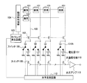
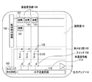
図8〜図10を参照して、本発明の第1の実施形態による撮像装置の動作原理を説明する。図8は撮像装置の構成を概略的に示す図である。撮像装置は、画素部10、タイミング発生回路103、垂直走査回路104、列メモリ部105、第1のスイッチ108、垂直信号線(第1の信号線)100、共通信号線110、水平走査回路112及び出力アンプ113を有する。画素部10は、2次元行列状に配置された複数の画素101を有する。列メモリ部105は、列毎に、スイッチ102及びメモリ容量C105を有する。タイミング発生回路103は、スイッチ102、垂直走査回路104及び水平走査回路112にタイミング信号を出力する。画素101は、光を電気信号に変換する光電変換を行う光電変換素子を有し、光電変換された電気信号を垂直信号線100に出力する。複数の垂直信号線100は、列毎に設けられ、各列の画素101に共通に接続され、複数の画素101によりそれぞれ信号が出力される。垂直走査回路104は、画素101を行単位で選択し、選択された画素101の電気信号を垂直信号線100に出力させる。複数のスイッチ102は、複数の垂直信号線100及び複数のメモリ容量C105の間にそれぞれ設けられる。スイッチ102がタイミング発生回路103の制御によりオンすると、複数のメモリ容量C105は複数の垂直信号線100の信号をそれぞれ蓄積する。複数の第1のスイッチ108は、複数のメモリ容量C105と共通信号線110との間にそれぞれ設けられる。メモリ容量C105は、一方の端子がスイッチ102及び108に接続され、他方の端子がスイッチ106に接続される。水平走査回路112の制御により、複数列の第1のスイッチ108が順次オンすると、複数列のメモリ容量C105に蓄積されている信号が順次、共通信号線110に伝達される。出力アンプ113は、共通信号線110に接続され、共通信号線110の信号を増幅して出力する。
(First embodiment)
The operation principle of the imaging apparatus according to the first embodiment of the present invention will be described with reference to FIGS. FIG. 8 is a diagram schematically showing the configuration of the imaging apparatus. The imaging device includes a pixel unit 10, a
図9は、図8の撮像装置におけるメモリ容量C105から出力アンプ113までの構成を抜き出し、寄生容量C110及び寄生抵抗R110を描き加えた図である。寄生容量C110は、共通信号線110の列毎の寄生容量である。寄生抵抗R110は、共通信号線110の列毎の寄生抵抗である。
FIG. 9 is a diagram in which the configuration from the memory capacitor C105 to the output amplifier 113 in the image pickup apparatus of FIG. 8 is extracted and a parasitic capacitor C110 and a parasitic resistor R110 are added. The parasitic capacitance C110 is a parasitic capacitance for each column of the
図10は、図9の一部の回路の等価回路図である。グランド電位(基準電位)ノード間には、メモリ容量C105、第1のスイッチ108のオン抵抗R108、共通信号線110の寄生抵抗R110及び共通信号線100の寄生容量C110が直列に接続される。電圧V105は、メモリ容量C105の端子間電圧である。信号電荷Q105は、メモリ容量C105に蓄積される電荷であり、第1のスイッチ108がオンすると、共通信号線110の寄生容量C110に移動し、共通信号線110上に電圧が現れる。信号電荷Q105を速やかに容量C110に移動させるには、第1のスイッチ108がオンした時に流れる電流をできる限り大きくなるようにすればよい。
FIG. 10 is an equivalent circuit diagram of a part of the circuit of FIG. A memory capacitor C105, an on-resistance R108 of the
具体的には、メモリ容量C105が信号を保持する期間に第1の参照電位をメモリ容量C105に供給する。そして、第1のスイッチ108がオンしている期間に、第1のスイッチ108がオンする前の共通信号線110の電位に対する電位差が第1の参照電位よりも大きい第2の参照電位を供給することで実現する。
Specifically, the first reference potential is supplied to the memory capacitor C105 during a period in which the memory capacitor C105 holds a signal. Then, during the period in which the
この動作をより詳細に説明する。まず、メモリ容量C105の参照電圧をグランド電位から正の電圧に一時的に変化させ、オン抵抗R108の2端子のうち、メモリ容量C105と接続されている方の端子電圧を上げて、オン抵抗R108に流れる電流を大きくすることで実現できる。メモリ容量C105の端子間電圧V105(t)は次式(1)で表わされ、寄生容量C110の端子間電圧V110(t)は次式(2)で表わされる。また、共通信号線110の信号電荷Q110(t)は次式(3)で表わされ、メモリ容量C105の信号電荷Q105(t)は次式(4)で表わされる。また、抵抗R108に流れる電流I(t)は次式(5)で表わされる。
This operation will be described in more detail. First, the reference voltage of the memory capacitor C105 is temporarily changed from the ground potential to a positive voltage, and the terminal voltage of the two terminals of the on-resistance R108 that is connected to the memory capacitor C105 is increased to increase the on-resistance R108. This can be achieved by increasing the current flowing through the. The terminal voltage V105 (t) of the memory capacitor C105 is expressed by the following expression (1), and the terminal voltage V110 (t) of the parasitic capacitor C110 is expressed by the following expression (2). Further, the signal charge Q110 (t) of the
V105(t)=Q105(t)/C105 ・・・(1)
V110(t)=Q110(t)/C110 ・・・(2)
Q110(t)=∫I(t)dt ・・・(3)
Q105(t)=Q105(0)−∫I(t)dt ・・・(4)
I(t)=(V105(t)−V110(t))/(R108+R110) ・・・(5)
V105 (t) = Q105 (t) / C105 (1)
V110 (t) = Q110 (t) / C110 (2)
Q110 (t) = ∫I (t) dt (3)
Q105 (t) = Q105 (0) −∫I (t) dt (4)
I (t) = (V105 (t) −V110 (t)) / (R108 + R110) (5)
式(3)は、寄生容量C110の初期電荷を0と仮定すると、寄生容量C110の電荷Q110(t)が寄生容量C110に流れ込む電流Iの時間積分値に等しいことを示す。式(4)は、メモリ容量C105の電荷Q105(t)がその初期電荷Q105(0)から電流I(t)の積分値を引いたものに等しいことを示す。式(5)は、電流I(t)が抵抗R108とR110に掛かる電圧を抵抗R108とR110の和で割ったものに等しいことを示しており、抵抗R108とR110に掛かる電圧はV105(t)とV110(t)との差電圧となる。 Equation (3) shows that assuming that the initial charge of the parasitic capacitor C110 is 0, the charge Q110 (t) of the parasitic capacitor C110 is equal to the time integral value of the current I flowing into the parasitic capacitor C110. Equation (4) indicates that the charge Q105 (t) of the memory capacitor C105 is equal to the initial charge Q105 (0) minus the integrated value of the current I (t). Equation (5) shows that the current I (t) is equal to the voltage applied to the resistors R108 and R110 divided by the sum of the resistors R108 and R110, and the voltage applied to the resistors R108 and R110 is V105 (t). And V110 (t).
第1のスイッチ108のオン時の抵抗R108がかかる電圧によらず一定とすると、電流I(t)はV105(t)が大きいほど大きくなることは式(5)から自明である。第1のスイッチ108がオン直後の状態を考えると、電荷Q110は0、したがって電圧V110も0なので寄生容量C110の端子間電圧V110の時間的増加率は、次式(6)となり、電圧V105(t)の初期値V105(0)に比例することが分かる。
From the equation (5), it is obvious that the current I (t) increases as V105 (t) increases if the resistance R108 when the
d{V110(t)}/dt=I(0)/C110=1/C110×V105(0)/(R108+R110) ・・・(6) d {V110 (t)} / dt = I (0) / C110 = 1 / C110 × V105 (0) / (R108 + R110) (6)
ここで、電圧V105(t)はメモリ容量C105の端子間電圧であるので、メモリ容量C105の参照電圧をグランド電位から正電圧VAに変化させると、オン抵抗R108に掛かる電圧もその分大きくなるので、電流I(0)の値は次式(7)へと増加する。 Here, since the voltage V105 (t) is a voltage between the terminals of the memory capacitor C105, if the reference voltage of the memory capacitor C105 is changed from the ground potential to the positive voltage VA, the voltage applied to the on-resistance R108 increases accordingly. The value of the current I (0) increases to the following equation (7).
I(0)=(VA+V105(0))/(R108+R110) ・・・(7) I (0) = (VA + V105 (0)) / (R108 + R110) (7)
以下、図1を参照しながら、メモリ容量C105の参照電圧をグランド電位から正電圧VAに変化させる回路構成について説明する。また、出力アンプ113から位置的に遠いメモリ容量C105からの信号ほど信号転送時の波形鈍りが大きいという課題に対しては、電圧源の電圧VAを全列等しい値にせず、出力アンプ113に近い列ほど低い値にする。これにより、上記高速化の効果を小さくし、波形鈍りをほぼ均一にすることで対処できる。 Hereinafter, a circuit configuration for changing the reference voltage of the memory capacitor C105 from the ground potential to the positive voltage VA will be described with reference to FIG. Further, for the problem that the waveform dullness at the time of signal transfer increases as the signal from the memory capacitor C105 located farther from the output amplifier 113, the voltage VA of the voltage source is not set to the same value in all columns, but is closer to the output amplifier 113. Set the value lower for the column. This can be dealt with by reducing the effect of increasing the speed and making the waveform dullness substantially uniform.
図1は、本発明の第1の実施形態による撮像装置の構成例を示す図である。図1の撮像装置は、図8の撮像装置に対して、基準電位切り換えスイッチ106及び電圧源107を追加したものである。以下、図1の撮像装置が図8の撮像装置と異なる点を説明する。複数の基準電位切り換えスイッチ106は、列毎に設けられ、各列のメモリ容量C108にそれぞれ接続される。電圧源107は、列毎に設けられ、電圧VAを出力する。各列の電圧源107は、出力アンプ113に近い列ほど低い電圧を出力し、出力アンプ113から遠い列ほど高い電圧を出力する。これにより、共通信号線110上において、各列の信号波形の鈍りを均一化し、特性を均一化することができる。メモリ容量C105は、一端がスイッチ102を介して垂直信号線100に接続され、他端が基準電位切り換えスイッチ106に接続される。水平走査回路112の制御により、列単位で、基準電位切り換えスイッチ106は、メモリ容量C105の他端を、グランド電位ノード又は電圧源107に接続する。メモリ容量C105の他端がグランド電位ノードに接続されると、メモリ容量C105の他端にグランド電位(0V)が供給される。メモリ容量C105の他端が電圧源107に接続されると、メモリ容量C105の他端に正電圧VAが供給される。
FIG. 1 is a diagram illustrating a configuration example of an imaging apparatus according to the first embodiment of the present invention. The imaging apparatus of FIG. 1 is obtained by adding a reference
2次元に配置された画素101の出力信号は、垂直走査回路104からのパルスで駆動され、各行が順次選択され、垂直信号線100に出力される。タイミング発生回路103からのパルスによって駆動されるスイッチ102がオンし、垂直信号線100の信号はメモリ容量C105に蓄積される。その時の、メモリ容量C105の参照電圧はグランド電位となるように、水平走査回路112の出力パルスによって基準電位切り換えスイッチ106はグランド電位ノード側に接続される。その後、水平走査回路112からの走査パルスによって各列の第1のスイッチ108が順次オンになり、メモリ容量C105に蓄積されている信号電荷が共通信号線110に転送される。この際、水平走査回路112からの走査パルスが出力されるタイミングに合わせて、基準電位切り換えスイッチ106が電圧源107側に接続されるように、水平走査回路112からのパルスで制御される。
The output signal of the
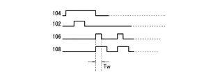
図2は、撮像装置の制御パルスを示すタイミング図である。垂直走査回路104のパルスがハイレベルの期間、そのパルスの行の画素101が選択され、選択された画素101の信号が垂直信号線100に出力される。スイッチ102の制御パルスがハイレベルの期間、スイッチ102がオンし、垂直信号線100の信号がメモリ容量C105に蓄積される。その時の基準電位切り換えスイッチ106の制御パルスはローレベルであり、基準電位切り換えスイッチ106はグランド電位ノード側に接続される。その後、複数列の第1のスイッチ108の制御パルスが順次ハイレベルになり、複数列の第1のスイッチ108が順次オンし、メモリ容量C108の信号電荷が共通信号線110に転送される。第1のスイッチ108の制御パルスのハイレベル期間内に、基準電位切り換えスイッチ106の制御パルスがハイレベルになる期間Twがあり、基準電位切り換えスイッチ106は電圧源107側に接続される。基準電位切り換えスイッチ106は、第1のスイッチ108がオフのときにはメモリ容量C105の他端にグランド電位を供給し、第1のスイッチ108がオンの期間内の少なくとも一部の期間Twにはメモリ容量C105の他端に正電圧VAを供給する。具体的には、基準電位切り換えスイッチ106は、第1のスイッチ108がオフのときにはメモリ容量C105の他端をグランド電位ノードに接続する。そして、基準電位切り換えスイッチ106は、第1のスイッチ108がオンの期間内の少なくとも一部の期間Twにはメモリ容量C105の他端を正電圧ノードに接続する。
FIG. 2 is a timing diagram illustrating control pulses of the imaging apparatus. While the pulse of the
上記動作によって、メモリ容量C105に蓄積されていた信号電荷は高速に共通信号線110に転送される。期間Twの適した値は、メモリ容量C105に蓄積されていた電荷の大部分が共通信号線110に転送される時間であればよい。具体的には、期間Twは、メモリ容量C105の容量値、スイッチ106と108のオン抵抗値、共通信号線110に付随する寄生容量C110とで決まる時定数の3倍が目安となる。しかし、上記時定数の3倍に限るものではない。
By the above operation, the signal charge accumulated in the memory capacitor C105 is transferred to the
図11は、図1の撮像装置のある列の一部の回路の等価回路図である。抵抗R108は、第1のスイッチ108のオン抵抗である。抵抗R110は、共通信号線110の寄生抵抗である。容量C110は、共通信号線110の寄生容量である。メモリ容量C105の一端とグランド電位ノード間には、オン抵抗R108、寄生抵抗R110及び寄生容量C110が直列に接続される。基準電位切り換えスイッチ106は、メモリ容量C105の他端をグランド電位ノード又は電圧源107に接続する。すなわち、基準電位切り換えスイッチ106は、メモリ容量C105の基準電位(参照電圧)をグランド電位又は正電圧VAに切り替える。基準電位切り換えスイッチ106が電圧源107側に接続されると、抵抗R108とR110に掛かる初期電圧はVA+V105(0)となる。その結果、上述したように、基準電位切り換えスイッチ106が切り替わった直後の電流I(0)が大きくなるため、式(6)から電圧V110の時間的変化率も大きくなる。このことは、メモリ容量C105から寄生容量C110へ信号電荷をより速く転送することを示している。すなわち、本実施形態は、メモリ容量C105の信号電荷を高速で共通信号線110に転送することができる。また、各列の電圧源107は、出力アンプ113から遠い列ほど高い電圧を出力することにより、共通信号線110上の各列の信号波形の鈍りを均一化し、特性を均一化することができる。
FIG. 11 is an equivalent circuit diagram of a partial circuit of a certain column of the imaging device of FIG. The resistor R108 is an on-resistance of the
図12は、図11の回路の他の構成例を示す図である。図12の回路が図11の回路と異なる点を説明する。メモリ容量C105の他端は、グランド電位ノードに固定接続される。寄生容量C110の一端は、抵抗R108及びR110を介してメモリ容量C105の一端に接続される。第3のスイッチ115は、寄生容量C110の他端を、グランド電位ノード又は負の電圧源114に接続する。第3のスイッチ115が負の電圧源114に接続されると、寄生量C110の他端には負電圧VBが供給される。メモリ容量C105の他端に接続されるグランド電位ノードの電圧は、寄生容量C110の他端に接続される負の電源電圧114の負電圧VBよりも高くなるため、図11の場合と同様に、メモリ容量C105の信号電荷は高速に共通信号線110に転送される。具体的には、第1のスイッチ108がオンに切り替わった直後に、第3のスイッチ115により容量C110の基準電位を、期間Tw、グランド電位から負電圧VBへ変化させる。複数の第3のスイッチ115は、容量C110を介して共通信号線110に接続される。第3のスイッチ115は、第1のスイッチ108がオフのときには容量C110を介して共通信号線110にグランド電位を供給する。そして、第1のスイッチ108がオンの期間内の少なくとも一部の期間Twには容量C110を介して共通信号線110に負電圧VBを供給する。これにより、第1のスイッチ108のオン後の初期電流が増大するため、高速信号転送が可能になる。なお、より具体的な回路構成は、後に図6を参照しながら説明する。
FIG. 12 is a diagram illustrating another configuration example of the circuit of FIG. The difference between the circuit of FIG. 12 and the circuit of FIG. 11 will be described. The other end of the memory capacitor C105 is fixedly connected to the ground potential node. One end of the parasitic capacitor C110 is connected to one end of the memory capacitor C105 via the resistors R108 and R110. The
(第2の実施形態)
図3は、本発明の第2の実施形態による撮像装置の構成例を示す図である。本実施形態は、第1の実施形態に対して、各列に配置されていた電圧源107の代わりに、1個の電圧源107と抵抗線による分圧回路を用いている点が異なる。1個の正の電圧源107とグランド電位ノード間には、抵抗線が接続される。抵抗線上には、所定間隔で複数列分の正電圧ノードを設ける。この抵抗分圧回路により、抵抗線上の各列の正電圧ノードには、出力アンプ113に近い列ほど低い電圧が生じる。各列の基準電位切り換えスイッチ106は、メモリ容量C105の他端を、グランド電位ノード又は各列の正電圧ノードに接続する。これにより、1個の電圧源107を用いて、共通信号線110上の信号波形の鈍りを均一化し、特性を均一化することができる。複数の基準電位切り換えスイッチ106は、それぞれ複数のメモリ容量C105の他端を複数の正電圧ノードに接続可能である。複数の正電圧ノードには、電圧源107及びグランド電位ノード間に接続された抵抗線により抵抗分割された電圧が供給される。本実施形態によれば、メモリ容量C105からの信号転送時の波形鈍りが列依存性を持つ問題を、電圧源107と抵抗分圧回路により、メモリ容量C105の基準電位を列毎に変化(暫減)させることで解決することができる。
(Second Embodiment)
FIG. 3 is a diagram illustrating a configuration example of an imaging apparatus according to the second embodiment of the present invention. This embodiment is different from the first embodiment in that a voltage source circuit using one
(第3の実施形態)
図4は本発明の第3の実施形態による撮像装置の構成例を示す図であり、図5は第3の実施形態による撮像装置のタイミング図である。図4の撮像装置は、図3の撮像装置に対して、電圧源107及び基準電位切り換えスイッチ106の代わりに可変電圧源121を設ける。可変電圧源121は、導通線又は抵抗線を介して各列のメモリ容量C105の他端に共通に接続され、複数のメモリ容量C105の他端にグランド電位又は正電圧VAを選択的に供給することができる。図5のタイミング図は、図2のタイミング図と同様である。ただし、可変電圧源112は、図2の基準電位切り換えスイッチ106と同様のタイミングで、ローレベルではグランド電位を出力し、ハイレベルでは正電圧VAを出力する。図5のタイミング図において、可変電圧源121は、期間Twで、グランド電位の出力から正電圧VAの出力に変化させる。正電圧VAの値は、撮像装置を実現する半導体プロセスが許す最大電圧まで増加させることが可能であり、高いほど高速化の効果が大きくなる。また、可変電圧源121の極性は、メモリ容量C105から転送され電荷の極性に依存し、正極性電荷であれば正電圧、負極性であれば負電圧とすることで高速転送の効果が得られる。
(Third embodiment)
FIG. 4 is a diagram illustrating a configuration example of an imaging apparatus according to the third embodiment of the present invention, and FIG. 5 is a timing diagram of the imaging apparatus according to the third embodiment. The image pickup apparatus in FIG. 4 is provided with a variable voltage source 121 instead of the
(第4の実施形態)
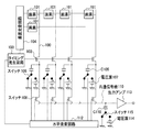
図6は本発明の第4の実施形態による撮像装置の構成例を示す図であり、図7は第4の実施形態による撮像装置のタイミング図である。図6の撮像装置は、図11と図12を組み合わせた図13のようにスイッチ106及び115を用いて、2つの容量C105及びC110の基準電位を同時に変化させた例である。図13の回路は、図11の回路に対して、第3のスイッチ115及び負の電圧源114を追加したものである。第3のスイッチ115は、寄生容量C110の他端を、グランド電位又は負の電圧源114に接続する。図6の撮像装置は、図1の撮像装置に対して、第3のスイッチ115及び負の電圧源114を追加したものである。寄生容量C110は、一端が共通信号線110に接続され、他端が第3のスイッチ115に接続される。第3のスイッチ115は、寄生容量C110の他端を、グランド電位又は負の電圧源114に接続する。以下、図7のタイミング図が図2のタイミング図と異なる点を説明する。第1のスイッチ108の制御パルスがハイレベルになると、第1のスイッチ108がオンし、メモリ容量C105に蓄積されている信号電荷は共通信号線110に転送される。第1のスイッチ108の制御パルスのハイレベル期間内の期間Twでは、スイッチ106及び115の制御パルスが同時にハイレベルになる。期間Tw以外では、スイッチ106及び115の制御パルスはローレベルになる。基準電位切り換えスイッチ106は、制御パルスがローレベルのときにはグランド電位ノードに接続され、制御パルスがハイレベルのときには正の電圧源107に接続される。第3のスイッチ115は、制御パルスがローレベルのときにはグランド電位ノードに接続され、制御パルスがハイレベルのときには負の電圧源114に接続される。期間Twでは、メモリ容量C105の基準電位はグランド電位から正電圧VAに切り替わり、共通信号線110の寄生容量C110の基準電位はグランド電位から負電圧VBに切り替わる。これにより、メモリ容量C105の基準電位は、共通信号線110の寄生容量C110の基準電位より高くなるので、メモリ容量C105の信号電荷を高速に共通信号線110に転送することができる。
(Fourth embodiment)
FIG. 6 is a diagram illustrating a configuration example of an imaging apparatus according to the fourth embodiment of the present invention, and FIG. 7 is a timing diagram of the imaging apparatus according to the fourth embodiment. The imaging apparatus of FIG. 6 is an example in which the reference potentials of the two capacitors C105 and C110 are changed simultaneously using the
(第5の実施形態)
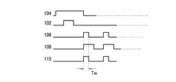
図14は本発明の第5の実施形態による撮像装置の構成例を示す図であり、図15は第5の実施形態による撮像装置のタイミング図である。図14の撮像装置は、第4の実施形態に対して、第4のスイッチ109及びブロック選択水平走査回路116を追加したものであり、読み出し回路ブロック122の選択を行うことができる。以下、本実施形態が第4の実施形態と異なる点を説明する。メモリ容量C105、基準電位切り換えスイッチ106、電圧源107及び第1のスイッチ108は、複数列を単位として、複数の読み出し回路ブロック112に分割される。各読み出し回路ブロック122内の第1のスイッチ108は、1個のスイッチ109に共通に接続される。第4のスイッチ109は、読み出し回路ブロック122毎に設けられ、一端が読み出し回路ブロック122内の全スイッチ108に接続され、他端が共通信号線110に接続される。ブロック選択水平走査回路116は、第4のスイッチ109のオン/オフを制御する。複数の第1のスイッチ108は、複数の読み出し回路ブロック122に分割される。複数の第4のスイッチ109は、各読み出し回路ブロック122内の第1のスイッチ108と共通信号線110との間に設けられ、複数の読み出し回路ブロック122を順次選択するために順次オンする。以下、図15のタイミングが図7のタイミング図と異なる点を説明する。第4のスイッチ109は、制御パルスがローレベルのときにオフし、制御パルスがハイレベルのときにオンする。複数の第4のスイッチ109は順次オンし、各読み出し回路ブロック122の信号は順次、共通信号線110に出力される。1個のスイッチ109の制御パルスがハイレベルになり、1個の読み出し回路ブロック122が選択されている期間内に、図7と同様に、その読み出し回路ブロック122内の全スイッチ108を順次オンさせる。第1のスイッチ108のオン期間内の期間Twでは、スイッチ106及び115を同時にオンすることにより、メモリ容量C105の信号電荷を高速に共通信号線110に転送することができる。
(Fifth embodiment)
FIG. 14 is a diagram illustrating a configuration example of an imaging apparatus according to the fifth embodiment of the present invention, and FIG. 15 is a timing diagram of the imaging apparatus according to the fifth embodiment. The imaging apparatus of FIG. 14 is obtained by adding a
第1、第2及び第5の実施形態では、スイッチ106及び電圧源107は、第1のスイッチ108がオンしている期間内に、メモリ容量C105の基準電位と共通信号線100の基準電位との差が大きくなるように基準電位を変化させる基準電位供給部である。また、図12では、上記の基準電位供給部は、第3のスイッチ115及び電圧源114である。また、第3の実施形態では、上記の基準電位供給部は、可変電圧源121である。また、第4の実施形態では、上記の基準電位供給部は、基準電位切り換えスイッチ106、電圧源107、第3のスイッチ115及び電圧源114である。
In the first, second, and fifth embodiments, the
上記の基準電位供給部は、上記の基準電位を変化させる際に、下記の状態になるように基準電位を制御する。共通信号線110上において出力アンプ113から遠い位置に接続されるメモリ容量C105と共通信号線110の基準電位の差が出力アンプ113に近い位置に接続されるメモリ容量C105と共通信号線110の基準電位の差よりも大きくなるように制御される。
The reference potential supply unit controls the reference potential so as to be in the following state when changing the reference potential. The difference between the reference potentials of the memory capacitor C105 and the
なお、上記実施形態は、何れも本発明を実施するにあたっての具体化の例を示したものに過ぎず、これらによって本発明の技術的範囲が限定的に解釈されてはならないものである。すなわち、本発明はその技術思想、又はその主要な特徴から逸脱することなく、様々な形で実施することができる。上記実施形態は、種々の組み合わせが可能である。 The above-described embodiments are merely examples of implementation in carrying out the present invention, and the technical scope of the present invention should not be construed in a limited manner. That is, the present invention can be implemented in various forms without departing from the technical idea or the main features thereof. Various combinations of the above embodiments are possible.
100 垂直信号線、101 画素、102 スイッチ、C105 メモリ容量、106 基準電位切り換えスイッチ、107 電圧源、108 第1のスイッチ、110 共通信号線 100 vertical signal line, 101 pixel, 102 switch, C105 memory capacity, 106 reference potential changeover switch, 107 voltage source, 108 first switch, 110 common signal line
Claims (6)
前記画素から出力された信号を保持する複数のメモリと、
前記複数のメモリに保持された信号を伝達する共通信号線と、
前記複数のメモリと前記共通信号線とをそれぞれ接続する複数の第1のスイッチと、を有する撮像装置であって、
前記複数のメモリの各々は、一方の端子には前記画素から出力された信号が与えられるとともに前記第1のスイッチと接続され、他方の端子に基準電位が与えられるメモリ容量を有し、
前記撮像装置は、さらに前記基準電位を供給する基準電位供給部を備え、
前記基準電位供給部は、前記複数のメモリが信号を保持する期間に第1の参照電位を供給し、前記第1のスイッチがオンしている期間に、前記第1のスイッチがオンする前の前記共通信号線の電位に対する電位差が前記第1の参照電位よりも大きい第2の参照電位を供給すること
を特徴とする撮像装置。 A plurality of pixels that output signals obtained by photoelectric conversion;
A plurality of memories for holding signals output from the pixels;
A common signal line for transmitting signals held in the plurality of memories;
A plurality of first switches that connect the plurality of memories and the common signal line, respectively,
Each of the plurality of memories has a memory capacity in which a signal output from the pixel is given to one terminal and connected to the first switch, and a reference potential is given to the other terminal.
The imaging apparatus further includes a reference potential supply unit that supplies the reference potential.
The reference potential supply unit supplies a first reference potential during a period in which the plurality of memories hold a signal, and before the first switch is turned on during a period when the first switch is on. An imaging apparatus, wherein a second reference potential having a potential difference with respect to the potential of the common signal line larger than the first reference potential is supplied.
前記基準電位供給部は、前記共通信号線上において前記出力アンプから遠い位置に接続される前記メモリ容量に与えられる前記第2の参照電位が前記出力アンプに近い位置に接続される前記メモリ容量に与えられる前記第2の参照電位よりも、前記第1のスイッチがオンする前の前記共通信号線の電位に対する電位差が大きくなるように基準電位を制御することを特徴とする請求項1記載の撮像装置。 And an output amplifier connected to the common signal line and amplifying the signal of the common signal line,
The reference potential supply unit applies the second reference potential applied to the memory capacitor connected to a position far from the output amplifier on the common signal line to the memory capacitor connected to a position close to the output amplifier. 2. The imaging apparatus according to claim 1, wherein the reference potential is controlled so that a potential difference with respect to the potential of the common signal line before the first switch is turned on is larger than the second reference potential. .
前記基準電位供給部は、前記複数のメモリ容量の他方の端子にそれぞれ接続される複数の基準電位切り換えスイッチを有し、
前記基準電位切り換えスイッチは、前記第1のスイッチがオフのときには対応する前記メモリ容量の他方の端子にグランド電位を供給し、前記第1のスイッチがオンの期間内の少なくとも一部の期間には対応する前記メモリ容量の他方の端子に正電圧を供給することを特徴とする請求項1又は2記載の撮像装置。 A first signal line for transmitting a signal output from the pixel;
The reference potential supply unit has a plurality of reference potential changeover switches connected to the other terminals of the plurality of memory capacitors,
The reference potential change-over switch supplies a ground potential to the other terminal of the corresponding memory capacitor when the first switch is off, and at least during a period during which the first switch is on. The imaging apparatus according to claim 1, wherein a positive voltage is supplied to the other terminal of the corresponding memory capacity.
前記複数の正電圧ノードは、電圧源及びグランド電位ノード間に接続された抵抗線により抵抗分割された電圧が供給されることを特徴とする請求項3記載の撮像装置。 The plurality of reference potential changeover switches can connect the other ends of the plurality of memory capacities to a plurality of positive voltage nodes, respectively.
4. The imaging apparatus according to claim 3, wherein the plurality of positive voltage nodes are supplied with a voltage divided by a resistance line connected between a voltage source and a ground potential node.
前記第3のスイッチは、前記第1のスイッチがオフのときには前記容量を介して前記共通信号線にグランド電位を供給し、前記第1のスイッチがオンの期間内の少なくとも一部の期間には前記容量を介して前記共通信号線に負電圧を供給することを特徴とする請求項1〜4のいずれか1項に記載の撮像装置。 The reference potential supply unit includes a plurality of third switches connected to the common signal line through a capacitor,
The third switch supplies a ground potential to the common signal line through the capacitor when the first switch is off, and during at least a part of the period during which the first switch is on. The imaging apparatus according to claim 1, wherein a negative voltage is supplied to the common signal line through the capacitor.
前記複数の第4のスイッチは、前記複数のブロックを順次選択するために順次オンすることを特徴とする請求項1〜5のいずれか1項に記載の撮像装置。 Further, the plurality of first switches are divided into a plurality of blocks, and a plurality of fourth switches provided between the first switch in each block and the common signal line are provided.
The imaging apparatus according to claim 1, wherein the plurality of fourth switches are sequentially turned on to sequentially select the plurality of blocks.
Priority Applications (3)
| Application Number | Priority Date | Filing Date | Title |
|---|---|---|---|
| JP2010135391A JP5484208B2 (en) | 2010-06-14 | 2010-06-14 | Imaging device |
| US13/106,935 US8638384B2 (en) | 2010-06-14 | 2011-05-13 | Imaging apparatus for high-speed signal reading |
| CN201110153366.9A CN102281404B (en) | 2010-06-14 | 2011-06-09 | Imaging apparatus |
Applications Claiming Priority (1)
| Application Number | Priority Date | Filing Date | Title |
|---|---|---|---|
| JP2010135391A JP5484208B2 (en) | 2010-06-14 | 2010-06-14 | Imaging device |
Publications (3)
| Publication Number | Publication Date |
|---|---|
| JP2012004679A JP2012004679A (en) | 2012-01-05 |
| JP2012004679A5 JP2012004679A5 (en) | 2013-07-25 |
| JP5484208B2 true JP5484208B2 (en) | 2014-05-07 |
Family
ID=45095955
Family Applications (1)
| Application Number | Title | Priority Date | Filing Date |
|---|---|---|---|
| JP2010135391A Expired - Fee Related JP5484208B2 (en) | 2010-06-14 | 2010-06-14 | Imaging device |
Country Status (3)
| Country | Link |
|---|---|
| US (1) | US8638384B2 (en) |
| JP (1) | JP5484208B2 (en) |
| CN (1) | CN102281404B (en) |
Families Citing this family (10)
| Publication number | Priority date | Publication date | Assignee | Title |
|---|---|---|---|---|
| JP5814539B2 (en) | 2010-11-17 | 2015-11-17 | キヤノン株式会社 | Imaging device |
| JP2015080178A (en) | 2013-10-18 | 2015-04-23 | キヤノン株式会社 | Imaging element, imaging device, camera, and method for driving imaging device |
| JP6300488B2 (en) | 2013-10-22 | 2018-03-28 | キヤノン株式会社 | Imaging device, solid-state imaging device, and camera |
| JP6391290B2 (en) | 2014-05-08 | 2018-09-19 | キヤノン株式会社 | Imaging device |
| US9979916B2 (en) | 2014-11-21 | 2018-05-22 | Canon Kabushiki Kaisha | Imaging apparatus and imaging system |
| JP6539149B2 (en) | 2015-08-13 | 2019-07-03 | キヤノン株式会社 | Imaging device and imaging system |
| US9900539B2 (en) | 2015-09-10 | 2018-02-20 | Canon Kabushiki Kaisha | Solid-state image pickup element, and image pickup system |
| JP6674219B2 (en) | 2015-10-01 | 2020-04-01 | キヤノン株式会社 | Solid-state imaging device and imaging system |
| JP6632421B2 (en) | 2016-02-22 | 2020-01-22 | キヤノン株式会社 | Solid-state imaging device and imaging device |
| JP6833531B2 (en) | 2017-01-30 | 2021-02-24 | キヤノン株式会社 | Solid-state image sensor |
Family Cites Families (14)
| Publication number | Priority date | Publication date | Assignee | Title |
|---|---|---|---|---|
| US5771070A (en) * | 1985-11-15 | 1998-06-23 | Canon Kabushiki Kaisha | Solid state image pickup apparatus removing noise from the photoelectric converted signal |
| JPH02107075A (en) | 1988-10-17 | 1990-04-19 | Hitachi Ltd | Solid-state image pickup device |
| JP3793016B2 (en) | 2000-11-06 | 2006-07-05 | キヤノン株式会社 | Solid-state imaging device and imaging system |
| JP3728260B2 (en) * | 2002-02-27 | 2005-12-21 | キヤノン株式会社 | Photoelectric conversion device and imaging device |
| EP1341377B1 (en) * | 2002-02-27 | 2018-04-11 | Canon Kabushiki Kaisha | Signal processing device for image pickup apparatus |
| JP2006033631A (en) * | 2004-07-20 | 2006-02-02 | Matsushita Electric Ind Co Ltd | Solid-state image pickup device and sampling circuit |
| JP2008170756A (en) | 2007-01-12 | 2008-07-24 | Sony Corp | Display device |
| JP4300492B2 (en) | 2007-03-13 | 2009-07-22 | ソニー株式会社 | Display device |
| JP5082532B2 (en) | 2007-03-26 | 2012-11-28 | ソニー株式会社 | Display device, driving method thereof, and electronic apparatus |
| JP2008250093A (en) | 2007-03-30 | 2008-10-16 | Sony Corp | Display device and driving method thereof |
| JP2009038531A (en) * | 2007-07-31 | 2009-02-19 | Panasonic Corp | Solid imaging apparatus, and driving method thereof |
| JP4375463B2 (en) | 2007-08-31 | 2009-12-02 | ソニー株式会社 | Display device and display method |
| JP2009124514A (en) | 2007-11-15 | 2009-06-04 | Sony Corp | Solid-state imaging device and camera system |
| JP5156434B2 (en) | 2008-02-29 | 2013-03-06 | キヤノン株式会社 | Imaging apparatus and imaging system |
-
2010
- 2010-06-14 JP JP2010135391A patent/JP5484208B2/en not_active Expired - Fee Related
-
2011
- 2011-05-13 US US13/106,935 patent/US8638384B2/en not_active Expired - Fee Related
- 2011-06-09 CN CN201110153366.9A patent/CN102281404B/en not_active Expired - Fee Related
Also Published As
| Publication number | Publication date |
|---|---|
| CN102281404B (en) | 2014-01-08 |
| JP2012004679A (en) | 2012-01-05 |
| US8638384B2 (en) | 2014-01-28 |
| US20110304756A1 (en) | 2011-12-15 |
| CN102281404A (en) | 2011-12-14 |
Similar Documents
| Publication | Publication Date | Title |
|---|---|---|
| JP5484208B2 (en) | Imaging device | |
| CN104869330B (en) | Photoelectric conversion device and image capture system | |
| JP5224942B2 (en) | Solid-state imaging device | |
| CN101257564B (en) | Photoelectric conversion apparatus and image sensing system using the same | |
| CN101729806B (en) | Solid-state image pickup apparatus, image pickup system | |
| US20190297296A1 (en) | Photoelectric conversion apparatus and image pickup system | |
| KR101595687B1 (en) | Solid-state image capture device | |
| JP2016040899A (en) | Photoelectric conversion device and imaging system | |
| CN102905088A (en) | Solid-state imaging apparatus | |
| CN106101586A (en) | Solid state image pickup device | |
| KR20110014089A (en) | Solid-state image sensing device, analog-digtal conversion method of solid-state image sensing device, and electronic apparatus | |
| CN104137421A (en) | A/d conversion circuit, and solid-state image pickup apparatus | |
| KR102344590B1 (en) | Imaging device and its control method | |
| JP6274904B2 (en) | Solid-state imaging device and imaging system | |
| KR101598748B1 (en) | Solid-state image capture device | |
| WO2018181582A1 (en) | Image pickup element, focus adjusting device, and image pickup device | |
| CN103988494B (en) | Solid state imaging device | |
| CN103681716A (en) | Image pickup apparatus, method of driving image pickup apparatus, and image pickup system | |
| CN103609097A (en) | Signal processing device for solid state image pick-up device and solid state image pick-up device | |
| JP2020114020A (en) | Image sensor and image-capturing device | |
| CN107197181A (en) | Image-forming component and imaging device | |
| CN101360454A (en) | Solid state imaging device | |
| CN103988495A (en) | Solid-state imaging device | |
| US20140048690A1 (en) | Solid-state imaging device | |
| WO2018143296A1 (en) | Imaging element and electronic camera |
Legal Events
| Date | Code | Title | Description |
|---|---|---|---|
| A521 | Request for written amendment filed |
Free format text: JAPANESE INTERMEDIATE CODE: A523 Effective date: 20130612 |
|
| A621 | Written request for application examination |
Free format text: JAPANESE INTERMEDIATE CODE: A621 Effective date: 20130612 |
|
| A977 | Report on retrieval |
Free format text: JAPANESE INTERMEDIATE CODE: A971007 Effective date: 20140109 |
|
| TRDD | Decision of grant or rejection written | ||
| A01 | Written decision to grant a patent or to grant a registration (utility model) |
Free format text: JAPANESE INTERMEDIATE CODE: A01 Effective date: 20140121 |
|
| A61 | First payment of annual fees (during grant procedure) |
Free format text: JAPANESE INTERMEDIATE CODE: A61 Effective date: 20140218 |
|
| LAPS | Cancellation because of no payment of annual fees |