JP5480168B2 - Reading reference technique to protect against current degradation - Google Patents
Reading reference technique to protect against current degradation Download PDFInfo
- Publication number
- JP5480168B2 JP5480168B2 JP2010550709A JP2010550709A JP5480168B2 JP 5480168 B2 JP5480168 B2 JP 5480168B2 JP 2010550709 A JP2010550709 A JP 2010550709A JP 2010550709 A JP2010550709 A JP 2010550709A JP 5480168 B2 JP5480168 B2 JP 5480168B2
- Authority
- JP
- Japan
- Prior art keywords
- current
- cell
- cells
- bit
- reference cell
- Prior art date
- Legal status (The legal status is an assumption and is not a legal conclusion. Google has not performed a legal analysis and makes no representation as to the accuracy of the status listed.)
- Expired - Fee Related
Links
Images


Classifications
-
- G—PHYSICS
- G11—INFORMATION STORAGE
- G11C—STATIC STORES
- G11C16/00—Erasable programmable read-only memories
- G11C16/02—Erasable programmable read-only memories electrically programmable
- G11C16/06—Auxiliary circuits, e.g. for writing into memory
- G11C16/26—Sensing or reading circuits; Data output circuits
- G11C16/28—Sensing or reading circuits; Data output circuits using differential sensing or reference cells, e.g. dummy cells
-
- G—PHYSICS
- G11—INFORMATION STORAGE
- G11C—STATIC STORES
- G11C11/00—Digital stores characterised by the use of particular electric or magnetic storage elements; Storage elements therefor
- G11C11/56—Digital stores characterised by the use of particular electric or magnetic storage elements; Storage elements therefor using storage elements with more than two stable states represented by steps, e.g. of voltage, current, phase, frequency
- G11C11/5621—Digital stores characterised by the use of particular electric or magnetic storage elements; Storage elements therefor using storage elements with more than two stable states represented by steps, e.g. of voltage, current, phase, frequency using charge storage in a floating gate
- G11C11/5642—Sensing or reading circuits; Data output circuits
-
- G—PHYSICS
- G11—INFORMATION STORAGE
- G11C—STATIC STORES
- G11C7/00—Arrangements for writing information into, or reading information out from, a digital store
- G11C7/14—Dummy cell management; Sense reference voltage generators
Landscapes
- Engineering & Computer Science (AREA)
- Computer Hardware Design (AREA)
- Read Only Memory (AREA)
Description
本開示は、一般に、メモリデバイスに関し、より具体的には、基準セルを利用した不揮発性メモリデバイスに関する。 The present disclosure relates generally to memory devices, and more specifically to non-volatile memory devices that utilize reference cells.
不揮発性メモリ(NVM)デバイスは、典型的に、各ビットセルがデータの対応するビットを記憶するビットセルのアレイからなる。各ビットセルは、一般に、電荷を蓄積しうる1つまたは複数のトランジスタとして構成されてトランジスタの制御電極電圧とドレイン電流との関係に影響を与える。トランジスタは電荷をクリアすることによって1つの状態(たとえば、論理「1」)に消去され、トランジスタはトランジスタに電荷を蓄積することによって別の状態(たとえば、論理「0」)に「プログラム」される。したがって、トランジスタによって「記憶された」ビット値は、トランジスタの制御電極への読取り電圧の印加に対応して基準(電流または電圧のいずれか)をトランジスタのドレイン電流と比較することによって検知され、「記憶された」値は、ドレイン電流が読取り基準よりも大きい場合に1つの状態(たとえば、論理「1」または「消去された」状態)であると判断され、ドレイン電流が読取り基準よりも小さい場合に別の状態(たとえば、論理「0」または「プログラムされた」状態)であると判断される。 Non-volatile memory (NVM) devices typically consist of an array of bit cells, where each bit cell stores a corresponding bit of data. Each bit cell is generally configured as one or more transistors capable of storing charge and affects the relationship between the control electrode voltage of the transistor and the drain current. A transistor is erased to one state (eg, logic “1”) by clearing the charge, and the transistor is “programmed” to another state (eg, logic “0”) by storing charge in the transistor. . Thus, the bit value “stored” by the transistor is sensed by comparing a reference (either current or voltage) with the drain current of the transistor in response to applying a read voltage to the control electrode of the transistor, A “stored” value is determined to be a state (eg, a logic “1” or “erased” state) when the drain current is greater than the read reference, and the drain current is less than the read reference. Is in a different state (eg, a logic “0” or “programmed” state).
従来のNVMアーキテクチャでは、読取り基準を発生するために基準セルを利用し、それによって、基準セルは、検知されているビットセルの特性を厳密に模倣すべくデータを記憶するために使用されるビットセルと似た構造にしてある。しかし、基準セルによって出力される基準電流は、典型的に、動作中に減少する。いくつかの条件下で、基準セルによって出力される読取り基準のこの劣化は、誤った読取りおよび書込み処理をもたらす可能性がある。連続処理またはほぼ連続的な処理のメモリを有する実施は、基準セルの劣化を特に受けやすい。したがって、メモリデバイスのビットセルを検知する基準セルの改良された実施方法が有利であることになる。 Traditional NVM architectures utilize a reference cell to generate a read reference, whereby the reference cell is a bit cell used to store data to closely mimic the characteristics of the bit cell being sensed. It has a similar structure. However, the reference current output by the reference cell typically decreases during operation. Under some conditions, this degradation of the read reference output by the reference cell can lead to erroneous read and write processing. Implementations with continuous or nearly continuous processing memory are particularly susceptible to reference cell degradation. Thus, an improved implementation of a reference cell that senses a bit cell of a memory device would be advantageous.
添付の図面を参照することによって、本開示はよりよく理解されるかもしれず、本開示の数多くの特徴および利点が当業者に明らかになるかもしれない。同じ参照記号を異なる図面において使用することによって、類似の項目または同じ項目を示す。 The present disclosure may be better understood and numerous features and advantages of the present disclosure may become apparent to those skilled in the art by reference to the accompanying drawings. The same reference symbols are used in different drawings to indicate similar or identical items.
前述のように、基準セルは、典型的に、その出力電流が連続処理中に減少するように劣化する。十分な処理期間を所与として、この劣化は基準セルの出力電流を最小閾値以下に低下させてメモリアクセス処理中にエラーを生じさせる可能性がある。劣化した基準セルの潜在的な出力電流が劣化発生前の最初の出力電流またはほぼ最初の出力電流まで時間とともに増加するような処理電圧では、基準セルがディセーブルされるかあるいは給電されなくなると、基準セルは、典型的に、復帰(または「緩和」)することを本発明者らは発見している。さらに、イネーブルされたときの基準セルの劣化速度とその後にディセーブルされたときの対応する緩和速度は、多くの場合、実質的に比例しており、多くの場合、所与の周囲温度に対して実質的に等しくなる可能性があることを本発明者らは発見している。したがって、少なくとも1つの実施形態において、不揮発性メモリ(NVM)デバイスのビットセルに記憶されたデータ値を検知するために一組の基準セルが使用される。事象に対応して、その組の最高出力(電流、あるいは電圧)を供給する基準セルは、後続のメモリアクセス処理に使用される基準セルとして選択される。その組の基準セルの残りの基準セルは、それらの最初の劣化状態またはほぼ最初の劣化状態まで復帰しうるようにディセーブルされる。各後続の事象において、一組の基準セルは、その時のその組の最高出力電流を供給する基準セルを識別するために再評価されうるし、NVMデバイスはこうして識別された基準セルを利用するように再構成されうる。読取り基準を供給するために最高出力電流(あるいは、電圧)を有する基準セルを利用するとともに残りの基準セルの1つまたは複数が復帰しうるように残りの基準セルをディセーブルすることによって、読取り基準が最小閾値以下に低下される可能性が低減または排除されて、ビットセルへのメモリアクセス処理中のエラーの可能性が少なくなる。 As mentioned above, the reference cell typically degrades so that its output current decreases during continuous processing. Given a sufficient processing period, this degradation can reduce the output current of the reference cell below the minimum threshold and cause an error during the memory access process. At a processing voltage where the potential output current of a degraded reference cell increases over time to the initial output current before degradation or nearly to the first output current, when the reference cell is disabled or no longer powered, We have found that the reference cell typically recovers (or “relaxes”). Furthermore, the degradation rate of the reference cell when enabled and the corresponding relaxation rate when subsequently disabled is often substantially proportional and often for a given ambient temperature. The present inventors have found that they can be substantially equal. Accordingly, in at least one embodiment, a set of reference cells is used to sense data values stored in bit cells of a non-volatile memory (NVM) device. In response to the event, the reference cell that provides the highest output (current or voltage) of the set is selected as the reference cell used for subsequent memory access processing. The remaining reference cells of the set of reference cells are disabled so that they can return to their first or near-first degradation state. In each subsequent event, a set of reference cells can be re-evaluated to identify the reference cell that supplies the set's highest output current at that time, and the NVM device can thus utilize the identified reference cell. Can be reconfigured. Read by utilizing the reference cell with the highest output current (or voltage) to provide the read reference and disabling the remaining reference cells so that one or more of the remaining reference cells can be restored The possibility of the criteria being reduced below the minimum threshold is reduced or eliminated, reducing the likelihood of errors during the memory access process to the bit cell.
説明を容易にするために、本開示の方法は、実施例を背景に記載され、検知基準は基準電流を備え、検知基準は2つの基準セルの一方の出力電流として選択されうる。しかし、本開示の方法は、本開示の範囲から逸脱することなく基準電圧を背景としてあるいは3つ以上の選択可能な基準セルを有する実施において利用されうる。 For ease of explanation, the method of the present disclosure is described in the context of an example, where the detection reference comprises a reference current, and the detection reference can be selected as the output current of one of the two reference cells. However, the method of the present disclosure can be utilized in the background with a reference voltage or with more than two selectable reference cells without departing from the scope of the present disclosure.
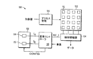
図1は、本開示の少なくとも1つの実施形態に従って不揮発性メモリ(NVM)デバイス100を示す。NVMデバイス100は、特定用途向け集積回路(ASIC)、または他のスタンドアロン・メモリ・デバイスなど、1つまたは複数の独立した集積回路(IC)として実施されうる。あるいは、NVMデバイス100は、たとえば、システム・オン・チップ(SOC)として実施されるマイクロプロセッサまたはマイクロコントローラなど、別のデバイスにおいて実施されうる。
FIG. 1 illustrates a non-volatile memory (NVM)
図示された実施例において、NVMデバイス100は、NVMアレイ102と、検知増幅器104と、アクセス管理モジュール106と、基準セルアレイ108と、基準コントローラ110とを含む。基準コントローラ110およびアクセス管理モジュール106は、たとえば、状態機械などのハードウェアベースの構成部品(たとえば、ディジタル論理構成部品)として構成されうる。NVMアレイ102は、NVMアレイ102の複数のビットセル112を備えるビット・セル・マトリクスを含む。NVMアレイ102は、たとえば、薄膜記憶装置(TFS)アーキテクチャ、高K誘電体またはナノ結晶アーキテクチャ、窒化物ベースアーキテクチャ、抵抗性メモリアーキテクチャ、磁気ランダム・アクセス・メモリ(MRAM)・アーキテクチャなど、様々な不揮発性メモリ・セル・アーキテクチャのいずれかを含みうる。説明を容易にするために、NVMアレイ102は、4×4ビット・セル・アレイとして図示さているが、実施において、NVMアレイ102は、典型的に、実質的にさらに多くのビットセルを含む。
In the illustrated embodiment,
NVMアレイ102は、供給されるアドレス(信号ADDR)に基づいてNVMアレイ102の記憶場所にアクセスするように構成される。少なくとも1つの実施形態において、各記憶場所は、複数のビット値からなるデータ値を記憶するためのデータフィールドを含む。検知増幅器104は、供給される基準電流REF_Iに基づいてアクセスされる記憶場所で一組のビットセルに記憶されたビット値を検知し、記憶場所で検知されたビット値をデータ値DATA[n−1:0]として供給するように構成される。特定の記憶場所にアクセス中に、電圧が記憶場所の複数のビットセルの各々の制御電極に印加され、検知増幅器104は対応するビットセルの結果として生じるドレイン電流を基準電流REF_Iと比較する。ビットセルのドレイン電流が基準電流REF_Iよりも大きい場合、DATA[n−1:0]の対応ビットに対する検知増幅器104の出力は、対応ビットセルに記憶された論理「1」の検知を示すために、たとえば、論理「1」としてアサートされる。逆に、ビットセルのドレイン電流が基準電流REF_Iよりも大きくない場合、対応するビットに対する検知増幅器104の出力は、対応ビットセルに記憶された論理「0」の検知を示すために、たとえば、論理「0」としてアサートされる。したがって、DATA[0:n−1]値のビットの各々に対して検知された値は、対応ビットセルのドレイン電流と基準電流REF_Iとの関係に基づいている。
The
基準セルアレイ108は、複数の基準セル(たとえば、基準セル114および115)を含み、各基準セルは、NVMアレイ102のビットセルを検知するときに基準電流REF_Iとして使用するために選択されうる出力電流(たとえば、IAおよびIB)を供給することができる。図1は2つの基準セルを有する基準セルアレイ108を示すが、2つよりも多い基準セルが利用されうる。さらに、基準セルアレイ108は、NVMアレイ102の種々のセクターなどの下位区分に対して種々の組の選択可能な基準セルに具体化されうる。少なくとも1つの実施形態において、基準セルアレイ108の基準セル114および115とNVMアレイ102のビットセル112とは、基準セル114および115がビットセル112の特性を模倣しうるように同じセル構成を有する。
基準コントローラ110は、電源投入事象、リセット事象、経過時間またはサイクル数、関連プロセッサによる特定命令の実行、関連プロセッサにおける特定割込みの発生、NVMデバイスの特定メモリアドレスへのアクセスなど、所定事象の発生に対応する事象インジケータを受け取るための入力を含む。所定事象の発生を示す事象インジケータのアサーションに対応して、基準コントローラ110は、信号CONFIGをアサートすることによって構成モードを開始する。構成モード中、基準コントローラ110は、一組の基準セルに対してどの基準セルが最高出力電流を発生するかを判断する。基準コントローラ110は、識別済みの基準セルをイネーブルされた状態に保って残りの基準セルの復帰を促すために残りの基準セルをディセーブルする。NVMアレイ102へのメモリアクセス処理では、基準コントローラ110は、その組のイネーブルされた基準セルの出力電流を基準電流REF_IとしてNVMアレイ102のビットセルに記憶されたデータを検知する検知増幅器104に供給する。
The reference controller 110 is responsible for the occurrence of certain events such as power-on events, reset events, elapsed time or number of cycles, execution of specific instructions by associated processors, occurrence of specific interrupts in related processors, access to specific memory addresses of NVM devices, etc. Contains an input to receive a corresponding event indicator. In response to an assertion of an event indicator indicating the occurrence of a predetermined event, the reference controller 110 initiates a configuration mode by asserting the signal CONFIG. During the configuration mode, the reference controller 110 determines which reference cell generates the highest output current for a set of reference cells. The reference controller 110 disables the remaining reference cells to keep the identified reference cells enabled and prompt the return of the remaining reference cells. In the memory access process to the
図2は、本開示の少なくとも1つの実施形態に従って図1の基準セルアレイ108および基準コントローラ110の実施を示す。図示された実施例において、基準セルアレイ108は、2つまたはそれ以上の電流(図2における電流IAおよびIB)を供給するように構成された規定構成201を含み、これらの電流の一方はNVMアレイ102(図1)のビットセルの検知に使用される基準電流REF_Iとして選択される。
FIG. 2 illustrates an implementation of the
図示された実施例において、規定構成201は、ワード・ライン・ドライバ206と、ワードライン207およびワードライン208と、ビットライン209およびビットライン210と、一組の4つの基準セル212、213、214、および215と、比較器216と、電流和モジュール218とを含む。基準セル214および215(それぞれREFAおよびREFB)は、動作基準セルであり、基準セル212および213は、基準セルアレイ108がNVMアレイ102(図1)と同じアレイアーキテクチャを有しうるように実施される非動作セル(すなわち、「ダミーセル」)である。基準セル214は、ビットライン209に接続された第1の電流電極と、電圧基準(たとえば、グラウンド)に接続された第2の電流電極と、ワードライン207に接続された制御電極とを備えるフローティング・ゲート・トランジスタを含む。基準セル215は、ビットライン210に接続された第1の電流電極と、電圧基準に接続された第2の電流電極と、ワードライン208に接続された制御電極とを含む。基準セル212および213は、ビットライン209および210に接続されていない。特定の1つのフローティングゲートの実施が基準セル212〜215に関して示されるが、他の基準セルアーキテクチャが本開示の範囲から逸脱することなく実施されうる。実例で説明すると、各基準セルは、2つまたはそれ以上のフローティング・ゲート・トランジスタを並列に含みうる。
In the illustrated embodiment, the
電流和モジュール218は、ビットライン209およびビットライン210に結合され、ビットライン209の電流IAとビットライン210の電流IBの和である基準電流REF_Iを発生するように構成される(ただし、電流IAおよび電流IBの一方または両方は以下に記載されるいくつかの状況において実質的にゼロの場合がある)。電流比較器216は、ビットライン209に結合された入力と、ビットライン210に結合された入力と、信号SELを供給するための出力とを含む。電流比較器216は、電流IAと電流IBの比較に基づいて信号SELをアサートまたは非アサート/アサート停止するように構成されてビットライン209と210のどちらが2つのビットラインの最高電流を有するかを示す。ワード・ライン・ドライバ206は、構成信号CONFIGを受け取るための入力と、信号SELを受け取るための入力と、基準セル214および215を別々にイネーブルまたはディセーブルするようにワードライン207および208を選択的に駆動するための出力とを含む。
リセット事象などの所定事象に対応して、基準コントローラ110はCONFIG信号を一時的にアサートする。CONFIG信号のアサーションに対応して、ワード・ライン・ドライバ206は、ワードライン207およびワードライン208の両方をアサートして、基準セル214のフローティング・ゲート・トランジスタにビットライン209の電流IAを駆動させ、基準セル215のフローティング・ゲート・トランジスタにビットライン210の電流IBを駆動させる。電流比較器216は、結果として生じる電流IAとIBを比較して信号SELが両電流の関係を反映するようにその出力を構成する。たとえば、電流比較器216は、電流IAが電流IBよりも大きいとき信号SELをアサートしうるし、電流IAが電流IBよりも小さいとき信号SELをアサート停止/非アサートしうる。
In response to a predetermined event, such as a reset event, the reference controller 110 temporarily asserts the CONFIG signal. In response to the assertion of the CONFIG signal, the
ワード・ライン・ドライバ206は、信号SELの状態をラッチし、信号SELの状態に基づいて2つの電流の大きい方の電流を供給している基準セルを識別する。この後、ワード・ライン・ドライバ206は、他の基準セルに関連するワードラインをアサート停止すると同時に識別された基準セルに関連するワードラインをアサートし続ける。実例で説明すると、基準セル214が2つの基準セル214および215の大きい方の出力電流を有するものと仮定すると、ワード・ライン・ドライバ206は、基準セル215をディセーブルするためにワードライン208をアサート停止し、電流IAを駆動し続けるために基準セル214をイネーブルされた状態に保つためにワードライン207をアサートし続ける。逆に、基準セル215が2つの基準セル214および215の大きい方の電流を有する場合には、ワード・ライン・ドライバ206は、基準セル214をディセーブルするためにワードライン207をアサート停止し、基準セル215をイネーブルされた状態に維持するためにワードライン208をアサートし続けることになる。
The
前述のように、電流和モジュール218は、電流IAと電流IBを合計して結果として得られる電流を基準電流REF_Iとして検知増幅器104(図1)に供給する。しかし、電流IAおよび電流IBの一方のみが、初期の構成モードの後、実質的に非ゼロであるので、基準電流REF_Iは、2つの基準セルの大きい方の電流を出力する基準セル214および215の一方の出力電流に等しい。別の実施形態において、電流和モジュール218は、ビットライン209またはビットライン210のいずれかを検知増幅器104の対応する入力に選択的に接続するように信号SELによって制御されるスイッチマトリクスとして実施されうる。
As described above, the
図2は2つの基準セルを実施する具体的な実施形態を示しており、2つの基準セルから基準電流を選択しうるが、2つより多い基準セルが本開示の範囲から逸脱することなく採用されうる。実例で説明すると、4つの基準セルが採用されうるし、構成信号CONFIGが事象に対応してアサートされるときに比較器216は4つの基準セルのどれが最高出力電流を駆動しているかを判断しうる。この後、ワード・ライン・ドライバ206は、電流和モジュール218によって出力される基準電流REF_Iが4つの基準セルの最高出力電流であるように残り3つの基準セルをディセーブルしうる。
FIG. 2 illustrates a specific embodiment that implements two reference cells, where a reference current can be selected from the two reference cells, but more than two reference cells are employed without departing from the scope of the present disclosure. Can be done. Illustratively, four reference cells may be employed, and when the configuration signal CONFIG is asserted in response to an event, the
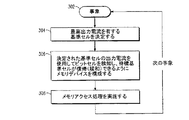
図3は、本開示の少なくとも1つの実施形態に従ってNVMデバイス100の処理方法300を示す。ブロック302において、所定事象がNVMデバイス100で検出される。所定事象は、たとえば、リセット事象(電源投入事象またはソフトリセット事象など)、特定割込みの発生(たとえば、タイマーによって発生される割込み)、特定命令の実行などを含む。
FIG. 3 illustrates a processing method 300 for the
事象の検出に対応して、ブロック304において、NVMデバイス100の基準コントローラ110は、基準セルアレイ108のどの基準セルが最高出力電流を供給するかを判断する。図2を参照して記載されたように、すべての基準セルをイネーブルした後で最高出力電流を識別するために電流比較器を用いることによって最高出力電流を有する基準セルが決定されうる。
In response to detecting the event, at
ブロック306において、基準コントローラ110は、NVMアレイ102のビットセルを検知するブロック304において識別される基準セルの出力電流を使用するようにNVMデバイス100を構成する。図2で示されるように、この構成は、最高出力電流を有する基準セルをイネーブルするために規定構成201のワード・ライン・ドライバ206を構成すること、規定構成201の出力電流がブロック304において識別される基準セルの出力電流に実質的に等しくなるように残りのすべての基準セルをディセーブルすることを含みうる。
In
ブロック308において、ブロック306において上記のように構成されたNVMデバイス100でメモリアクセス処理が実行されうる。ブロック306において実行された構成は、ブロック302の次の反復で別の所定事象が発生するまでブロック308におけるメモリアクセス処理に対して継続されうるし、別の所定事象が発生した時点で基準セルはブロック304において再評価されうるし、NVMデバイス100はブロック306において必要に応じて再構成されうる。方法300の次の反復に対する所定事象は、方法300の前の反復における事象と同じ事象または異なる事象を含みうる。
At
図4および5は、本開示の少なくとも1つの実施形態に従って図1および2のNVMデバイス100の様々な処理例を示すグラフである。両グラフでは、2つの基準セルREFAおよびREFB(たとえば、基準セル214および215、図2)がNVMアレイ102のビットセルにおけるデータ値を検知する基準電流を供給することができる。
4 and 5 are graphs illustrating various example processes of the
図4において、グラフ400は、基準セルREFAの出力電流を表わす線402と基準セルREFBの出力電流を表わす線404とともに、2つの基準セルREFAおよびREFBの出力電流(または潜在的な出力電流)を経時的に図示したものである。線402および404では、実線は、対応する時間における対応する基準セルの実際の出力電流を表わし、破線は、基準セルがその時点でイネーブルされることがあれば、対応する基準セルが対応する時間において発生させうるはずである出力電流を表わす。
In FIG. 4,
時間t0において、NVMデバイス100の電源が投入される(事象1)。それに応じて、基準コントローラ110は、どの基準セルが最高出力電流を有するかを判断する。この実施例では、最高出力電流を有するのは基準セルREFBであると仮定する。したがって、基準コントローラ110は、基準セルREFAをディセーブルし、基準セルREFBの出力電流を、ビットセルを検知する基準電流として利用する。線404で示されるように、基準セルREFBの出力電流は、最大出力電流I_Highから最小基準電流I_Minに向かう動作中、エラーを検知する前に劣化する。最小基準電流I_Minにまで劣化する前に、別の事象(たとえば、ソフトリセットまたはタイマー経過)が時間t1において発生する。それに応じて、基準コントローラ110は、基準セルREFAおよびREFBの両方をイネーブルしてどちらがより高い出力電流を供給するかを判断する。図4の例において、基準セルREFAは、時間t1に至るまでの動作による基準セルREFBの劣化に起因して時間t1において最高出力電流を供給する。したがって、基準コントローラ110は、基準セルREFBをディセーブルして、基準セルREFAの出力電流を時間t1の後でNVMアレイ102のビットセルを検知する基準電流REF_Iとして利用する。
At time t 0 , the
線402で示されるように、基準セルREFAの出力電流は、時間t1の後の動作中に劣化する。逆に、線404で示されるように、ディセーブルされた基準セルREFBは、時間t1の後に復帰または「緩和」しうる。したがって、時間t2において、または時間t2の前に、基準セルREFAの出力電流は、基準セルREFBの潜在的な出力電流よりも小さくなる。それ故に、別の事象が時間t2において発生すると、両方が事象に対応して再評価されるとき基準セルREFBは2つの基準の大きい方の出力電流を供給する。したがって、基準コントローラ110は、基準セルREFAをディセーブルしてイネーブルされた基準セルREFBの出力電流を時間t2の後にNVMアレイ102のビットセルを検知する基準電流として利用する。その一方で、ディセーブルされた基準セルREFAは、基準セルREFBが使用されている間に復帰しうる。時間t3において、別の事象が発生し、基準セルREFAおよびREFBの出力電流を選択するための再評価が再び行なわれる。
As indicated by
グラフ400で示されるように、その組の他の基準セルをディセーブルする一方で検知のための基準セルとして最高出力電流を有する基準セルを選択して利用することによって、その組の基準セルは、使用と不使用が交互に繰り返されて、ある期間中に使用されている基準セルを次の期間中にその最初の出力電流に復帰させることができる。結果的に、基準電流は、最小基準電流I_Minよりも高いレベルに維持されうる。対照的に、線406で示されるように、単一基準セルの従来の使用法では、最終的に、その出力電流、したがって、ビットセルの検知に使用される基準電流が典型的に検知エラーにつながる最小基準電流I_Min以下の点にまで単一基準セルを劣化させる可能性がある。
By selecting and utilizing the reference cell with the highest output current as a reference cell for sensing while disabling the other reference cells of the set, as shown in
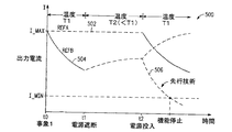
図5は、2つの基準セルREFAおよびREFBの経時的な出力電流(または、潜在的な出力電流)のグラフ500を、基準セルREFAの出力電流を表わす線502と基準セルREFBの出力電流を表わす線504で同様に示す。線502および504では、実線は、対応する時間における対応する基準セルの実際の出力電流を表わし、破線は、基準セルがその時点でイネーブルされることがあれば、対応する基準セルが対応する時間において発生させうるはずである出力電流を表わす。
FIG. 5 shows a
時間t0において、NVMデバイス100の電源が投入される。それに応じて、基準コントローラ110は、どの基準セルが最高出力電流を有するかを判断する。この実施例では、最高出力電流を有するのは基準セルREFBであると仮定する。したがって、基準コントローラ110は、基準セルREFAをディセーブルし、基準セルREFBの出力電流を、ビットセルを検知する基準電流として利用する。線504で示されるように、基準セルREFBの出力電流は、最大出力電流I_Highから最小基準電流I_Minに向かう動作中に劣化する。この実施例では、NVMデバイス100が温度T1(たとえば、85℃)で動作しているものと仮定する。
At time t 0 , the
NVMデバイス100の電源は、この後、時間t1とt2の間に遮断され、これによって、基準セルREFAおよびREFBの両方をディセーブルする。結果的に、基準セルREFBは、復帰を開始することができる。しかし、時間t1とt2との間の期間に、NVMデバイス100は、T2(たとえば、25℃)の比較的低い周囲温度にある。それ故に、基準セルの復帰速度はその温度にある程度比例するので、基準セルREFBは、NVMデバイス100の電源が再び投入される時間(時間t2)までに完全には復帰していない。したがって、基準セルREFAは、時間t2において比較的高い出力電流を有しており、基準コントローラ110は、したがって、時間t2の後のビットセルを検知する基準電流を供給するために基準セルREFAを選択する。しかし、NVMデバイス100の温度は時間t2の後の動作中に温度T1まで上昇するので、基準セルREFBは、より高速で復帰することができ、したがって、時間t2の後の動作中に基準セルREFAの劣化に起因して発生する次の事象に対応して選択されることになる。
The power supply of
グラフ500で示されるように、比較的低い温度に起因して復帰速度が低下している場合でも、比較的低い出力電流を有する基準セルをより完全に復帰させることによって最小電流I_Minよりも高い基準電流が維持されうる。対照的に、線506で示されるように、単一基準セルの従来の使用法では、最終的に、その出力電流、したがって、ビットセルの検知に使用される基準電流が最小基準電流I_Min以下の点にまで単一基準セルを劣化させる可能性がある。
As shown in
本開示の一態様に従って、メモリデバイスのビット・セル・アレイの複数のビットセルに関連する複数の基準セルの選択基準セルが、複数の基準セルの最高出力電流を有するものとして最初に決定される。複数のビットセルのビットセルに記憶されるデータ値は、選択基準セルの出力電流を用いて検知される。 In accordance with one aspect of the present disclosure, a selected reference cell of a plurality of reference cells associated with a plurality of bit cells of a bit cell array of a memory device is first determined as having the highest output current of the plurality of reference cells. Data values stored in the bit cells of the plurality of bit cells are detected using the output current of the selected reference cell.
本開示の別の態様に従って、ビット・セル・アレイと、ビット・セル・アレイの複数のビットセルに関連する複数の基準セルと、検知増幅器とを備えるメモリが提供される。第1の基準セルの出力電流が第1の事象における第1の複数の基準セルの最高出力電流であるとの判断に対応して、第1の事象において検知増幅器は複数の基準セルの第1の基準セルの出力電流を利用するように構成される。第2の基準セルの出力電流が第1の事象に続く第2の事象における複数の基準セルの最高出力電流であるとの判断に対応して、第2の事象において検知増幅器は複数の基準セルの第2の基準セルの出力電流を利用するように構成される。 In accordance with another aspect of the present disclosure, a memory is provided that includes a bit cell array, a plurality of reference cells associated with a plurality of bit cells of the bit cell array, and a sense amplifier. In response to determining that the output current of the first reference cell is the highest output current of the first plurality of reference cells in the first event, the sense amplifier in the first event includes the first of the plurality of reference cells. Are configured to utilize the output current of the reference cell. In response to determining that the output current of the second reference cell is the highest output current of the plurality of reference cells in the second event following the first event, the sense amplifier has a plurality of reference cells in the second event. Is configured to utilize the output current of the second reference cell.
本開示のさらに別の態様に従って、メモリデバイスが提供される。メモリデバイスは、複数のビットセルを備えるビット・セル・アレイと、複数のビットセルに関連する複数の基準セルとを含む。メモリデバイスは基準電流を受け取るための入力を備える検知増幅器をさらに含み、検知増幅器は基準電流に基づいてビット・セル・アレイのビットセルに記憶されたデータ値を検知するように構成される。また、メモリデバイスは、選択基準セルが複数の基準セルの最高出力電流を有するとの判断に対応して複数のビットセルのビットセルを検知する基準電流として、複数の基準セルの選択基準セルの出力電流を検知増幅器に供給するように構成された基準コントローラを備える。 In accordance with yet another aspect of the present disclosure, a memory device is provided. The memory device includes a bit cell array comprising a plurality of bit cells and a plurality of reference cells associated with the plurality of bit cells. The memory device further includes a sense amplifier having an input for receiving a reference current, wherein the sense amplifier is configured to sense a data value stored in a bit cell of the bit cell array based on the reference current. In addition, the memory device outputs the output current of the selected reference cell of the plurality of reference cells as a reference current for detecting the bit cell of the plurality of bit cells in response to determining that the selected reference cell has the highest output current of the plurality of reference cells. With a reference controller configured to supply a sense amplifier to the sense amplifier.
前述の説明は、不揮発性メモリに関する読取り基準の調整を含む、多くの具体的な実施形態および詳細を提供することによって、本開示の完全な理解を伝えることが意図されている。しかし、本開示は、これら具体的な実施形態および詳細に限定されるものではなく、これら具体的な実施形態および詳細は単なる例示であり、本開示の範囲は、したがって、以下の特許請求の範囲およびそれらの均等物のみによって限定されるものであることが理解される。当業者は、公知のシステムおよび方法に照らし、具体的な設計などの必要性に応じて意図する目的および利益のために数多くの代替的実施形態で本開示を採用することを評価するはずであることがさらに理解される。 The foregoing description is intended to convey a complete understanding of the present disclosure by providing many specific embodiments and details, including adjustment of read criteria for non-volatile memory. However, the present disclosure is not limited to these specific embodiments and details, which are merely exemplary and the scope of the present disclosure is therefore the following claims. It is understood that this is limited only by the equivalents thereof. Those skilled in the art will appreciate in light of known systems and methods that the present disclosure may be employed in numerous alternative embodiments for intended purposes and benefits depending on specific design and other needs. It is further understood.
本明細書において、「第1の」および「第2の」などの関連語は、上記の構成要素間または動作間の上記の関係または順序を必ずしも必要とせずにあるいは暗示せずに、1つの構成要素または動作を別の構成要素または動作と区別するためにのみ使用されてもよい。「備える」という用語あるいはこれらの変形形態は、要素のリストを備えるプロセス、方法、品目、あるいは装置がこれらの要素のみを含むのではなく、明示的に列挙されていない他の要素、あるいはこのようなプロセス、方法、品目、または装置に固有の要素を含んでいてもよいように、非排他的包含を網羅することが意図されている。本明細書において使用される「別の」という用語は、「少なくとも第2またはそれ以上の」として定義される。「含む」、「有する」という用語あるいはこれらの変形形態は、「備える」と定義される。電気光学技術に関連して本明細書において使用される「結合される」という用語は、必ずしも直接的ではなく、また必ずしも機械的ではないが、「接続される」と定義される。 In this specification, related terms such as “first” and “second” may refer to one or more of the above relationships or sequences between components or operations without necessarily necessitating or implying It may only be used to distinguish one component or action from another. The term “comprising” or variations thereof does not mean that a process, method, item, or apparatus comprising a list of elements includes only these elements, but other elements not explicitly listed, or such It is intended to cover non-exclusive inclusions that may include elements unique to a particular process, method, item, or apparatus. The term “another” as used herein is defined as “at least a second or more”. The terms “including”, “having” or variations thereof are defined as “comprising”. The term “coupled” as used herein in connection with electro-optic technology is defined as “connected”, although not necessarily directly and not necessarily mechanical.
Claims (5)
第1の時間における複数の基準セルの最高出力電流を有するものとして、メモリデバイスのビット・セル・アレイの複数のビットセルに関連する前記複数の基準セルの第1の基準セルを前記第1の時間において決定すること、
前記第1の基準セルの第1の出力電流を用いて前記複数のビットセルの第1のビットセルに記憶されたデータ値を検知すること
を備える方法。 A method,
The first reference cell of the plurality of reference cells associated with the plurality of bit cells of the bit cell array of the memory device is defined as having the highest output current of the plurality of reference cells at the first time. Determining in
Detecting a data value stored in a first bit cell of the plurality of bit cells using a first output current of the first reference cell.
前記第2の時間の後の第2の期間に前記複数の基準セルの第2の基準セルを除く前記複数の基準セルの各基準セルをディセーブルすること
をさらに備える、請求項1に記載の方法。 Disabling each reference cell of the plurality of reference cells excluding the first reference cell in a first period between the first time and a second time following the first time ;
2. The method of claim 1, further comprising disabling each reference cell of the plurality of reference cells excluding a second reference cell of the plurality of reference cells in a second period after the second time. Method.
複数のビットセルを備えるビット・セル・アレイと、
前記複数のビットセルに関連する複数の基準セルと、
基準電流を受け取るための入力を備える検知増幅器であって、前記基準電流に基づいて前記ビット・セル・アレイのビットセルに記憶されたデータ値を検知するように構成される前記検知増幅器と、
前記複数の基準セルの第1の基準セルの出力電流を、前記複数の基準セルの最高出力電流を有するものとして前記第1の基準セルを決定することに対応して、前記複数のビットセルのビットセルを検知する前記基準電流として前記検知増幅器に供給するように構成される基準コントローラと
を備えるメモリデバイス。 A memory device,
A bit cell array comprising a plurality of bit cells;
A plurality of reference cells associated with the plurality of bit cells;
A sense amplifier comprising an input for receiving a reference current, the sense amplifier configured to sense a data value stored in a bit cell of the bit cell array based on the reference current;
The bit cells of the plurality of bit cells in response to determining the first reference cell as having an output current of a first reference cell of the plurality of reference cells having a maximum output current of the plurality of reference cells; And a reference controller configured to supply the sense amplifier as the reference current for detecting a memory device.
前記複数の基準セルの第1の基準セルの電流電極に結合された第1の入力と、前記複数の基準セルの第2の基準セルの電流電極に結合された第2の入力とを備える比較器であって、前記第1の入力で検出される第1の電流と第2の入力で検出される第2の電流との比較を表す出力値を供給するように構成される前記比較器と、
前記複数の基準セルの前記第1の基準セルの制御電極に結合された第1のワードラインと、前記第2の基準セルの制御電極に結合された第2のワードラインとを備えるワード・ライン・ドライバであって、前記比較器の前記出力値に基づいて前記第1のワードラインと前記第2のワードラインの一方を選択的にイネーブルするように構成される前記ワード・ライン・ドライバと
を備える、請求項3に記載のメモリデバイス。 The reference controller is
A comparison comprising a first input coupled to a current electrode of a first reference cell of the plurality of reference cells and a second input coupled to a current electrode of a second reference cell of the plurality of reference cells. A comparator configured to provide an output value representative of a comparison between a first current detected at the first input and a second current detected at a second input; ,
A word line comprising: a first word line coupled to the control electrode of the first reference cell of the plurality of reference cells; and a second word line coupled to the control electrode of the second reference cell. A driver, the word line driver configured to selectively enable one of the first word line and the second word line based on the output value of the comparator; The memory device of claim 3, comprising:
Applications Claiming Priority (3)
| Application Number | Priority Date | Filing Date | Title |
|---|---|---|---|
| US12/048,683 | 2008-03-14 | ||
| US12/048,683 US7742340B2 (en) | 2008-03-14 | 2008-03-14 | Read reference technique with current degradation protection |
| PCT/US2009/031945 WO2009114213A1 (en) | 2008-03-14 | 2009-01-26 | Read reference technique with current degradation protection |
Publications (3)
| Publication Number | Publication Date |
|---|---|
| JP2011514615A JP2011514615A (en) | 2011-05-06 |
| JP2011514615A5 JP2011514615A5 (en) | 2012-03-15 |
| JP5480168B2 true JP5480168B2 (en) | 2014-04-23 |
Family
ID=41062885
Family Applications (1)
| Application Number | Title | Priority Date | Filing Date |
|---|---|---|---|
| JP2010550709A Expired - Fee Related JP5480168B2 (en) | 2008-03-14 | 2009-01-26 | Reading reference technique to protect against current degradation |
Country Status (4)
| Country | Link |
|---|---|
| US (1) | US7742340B2 (en) |
| EP (1) | EP2266117A4 (en) |
| JP (1) | JP5480168B2 (en) |
| WO (1) | WO2009114213A1 (en) |
Families Citing this family (3)
| Publication number | Priority date | Publication date | Assignee | Title |
|---|---|---|---|---|
| JP6260832B2 (en) * | 2012-10-30 | 2018-01-17 | パナソニックIpマネジメント株式会社 | Nonvolatile semiconductor memory device |
| US9595340B2 (en) * | 2015-01-20 | 2017-03-14 | Taiwan Semiconductor Manufacturing Company Limited | Nonvolatile memory device and method of setting a reference current in a nonvolatile memory device |
| WO2019177585A1 (en) | 2018-03-13 | 2019-09-19 | Rovi Guides, Inc. | Systems and methods for displaying a notification at an area on a display screen that is within a line of sight of a subset of audience members to whom the notification pertains |
Family Cites Families (10)
| Publication number | Priority date | Publication date | Assignee | Title |
|---|---|---|---|---|
| EP0632464B1 (en) * | 1993-06-28 | 1999-09-08 | STMicroelectronics S.r.l. | Method of measuring the current of microcontroller memory cells and relative system |
| US6097632A (en) * | 1997-04-18 | 2000-08-01 | Micron Technology, Inc. | Source regulation circuit for an erase operation of flash memory |
| JP2000268584A (en) | 1999-03-15 | 2000-09-29 | Nec Corp | Nonvolatile semiconductor storage device and its manufacture |
| US6396741B1 (en) | 2000-05-04 | 2002-05-28 | Saifun Semiconductors Ltd. | Programming of nonvolatile memory cells |
| JP4212760B2 (en) * | 2000-06-02 | 2009-01-21 | 富士通マイクロエレクトロニクス株式会社 | Semiconductor memory device |
| FR2820539B1 (en) | 2001-02-02 | 2003-05-30 | St Microelectronics Sa | METHOD AND DEVICE FOR COOLING REFERENCE CELLS |
| DE60129928D1 (en) * | 2001-04-19 | 2007-09-27 | St Microelectronics Srl | Method and circuit for timing the dynamic readout of a memory cell with control of the integration time |
| US6813189B2 (en) * | 2002-07-16 | 2004-11-02 | Fujitsu Limited | System for using a dynamic reference in a double-bit cell memory |
| JP2004062922A (en) | 2002-07-25 | 2004-02-26 | Renesas Technology Corp | Nonvolatile semiconductor memory device |
| US7180782B2 (en) | 2005-06-10 | 2007-02-20 | Macronix International Co., Ltd. | Read source line compensation in a non-volatile memory |
-
2008
- 2008-03-14 US US12/048,683 patent/US7742340B2/en not_active Expired - Fee Related
-
2009
- 2009-01-26 JP JP2010550709A patent/JP5480168B2/en not_active Expired - Fee Related
- 2009-01-26 WO PCT/US2009/031945 patent/WO2009114213A1/en active Application Filing
- 2009-01-26 EP EP09720623A patent/EP2266117A4/en not_active Withdrawn
Also Published As
| Publication number | Publication date |
|---|---|
| EP2266117A4 (en) | 2011-07-06 |
| EP2266117A1 (en) | 2010-12-29 |
| US20090231925A1 (en) | 2009-09-17 |
| JP2011514615A (en) | 2011-05-06 |
| US7742340B2 (en) | 2010-06-22 |
| WO2009114213A1 (en) | 2009-09-17 |
Similar Documents
| Publication | Publication Date | Title |
|---|---|---|
| US9922684B2 (en) | Memory device ultra-deep power-down mode exit control | |
| US7843741B2 (en) | Memory devices with selective pre-write verification and methods of operation thereof | |
| CN107615387B (en) | Memory device and method of controlling ultra-deep power down mode in memory device | |
| US7564716B2 (en) | Memory device with retained indicator of read reference level | |
| US8730712B2 (en) | SRAM including write assist circuit and method of operating same | |
| US7542354B2 (en) | Reprogrammable nonvolatile memory devices and methods | |
| US6677804B2 (en) | Dual bandgap voltage reference system and method for reducing current consumption during a standby mode of operation and for providing reference stability during an active mode of operation | |
| US10539989B1 (en) | Memory device alert of completion of internally self-timed power-up and reset operations | |
| KR20200107791A (en) | Techniques to mitigate selection failure for a memory device | |
| TWI384480B (en) | Memory and reading method thereof | |
| US9852090B2 (en) | Serial memory device alert of an external host to completion of an internally self-timed operation | |
| US10521154B2 (en) | Automatic switch to single SPI mode when entering UDPD | |
| KR20120104276A (en) | Refresh architecture and algorithm for non-volatile memories | |
| US20140177355A1 (en) | Nonvolatile memory apparatus | |
| US6643804B1 (en) | Stability test for silicon on insulator SRAM memory cells utilizing bitline precharge stress operations to stress memory cells under test | |
| KR20140112349A (en) | Retention logic for non-volatile memory | |
| US10891998B2 (en) | Memory device operating based on a write current for a given operation condition and a method of driving the write current | |
| US8199577B2 (en) | Ripple programming of memory cells in a nonvolatile memory | |
| JP5480168B2 (en) | Reading reference technique to protect against current degradation | |
| JP4100985B2 (en) | Data processing device, semiconductor memory device, and clock frequency detection method | |
| US9318164B2 (en) | Semiconductor memory device with power-saving signal | |
| US20230280915A1 (en) | Static random access memory supporting a single clock cycle read-modify-write operation with a modulated word line assertion | |
| US20230050783A1 (en) | Static random access memory supporting a single clock cycle read-modify-write operation |
Legal Events
| Date | Code | Title | Description |
|---|---|---|---|
| A521 | Written amendment |
Free format text: JAPANESE INTERMEDIATE CODE: A523 Effective date: 20120120 |
|
| A621 | Written request for application examination |
Free format text: JAPANESE INTERMEDIATE CODE: A621 Effective date: 20120120 |
|
| RD04 | Notification of resignation of power of attorney |
Free format text: JAPANESE INTERMEDIATE CODE: A7424 Effective date: 20120227 |
|
| A131 | Notification of reasons for refusal |
Free format text: JAPANESE INTERMEDIATE CODE: A131 Effective date: 20130402 |
|
| A521 | Written amendment |
Free format text: JAPANESE INTERMEDIATE CODE: A523 Effective date: 20130701 |
|
| TRDD | Decision of grant or rejection written | ||
| A01 | Written decision to grant a patent or to grant a registration (utility model) |
Free format text: JAPANESE INTERMEDIATE CODE: A01 Effective date: 20140114 |
|
| A61 | First payment of annual fees (during grant procedure) |
Free format text: JAPANESE INTERMEDIATE CODE: A61 Effective date: 20140213 |
|
| R150 | Certificate of patent or registration of utility model |
Ref document number: 5480168 Country of ref document: JP Free format text: JAPANESE INTERMEDIATE CODE: R150 |
|
| LAPS | Cancellation because of no payment of annual fees |