JP5467864B2 - Device for providing light radiation - Google Patents
Device for providing light radiation Download PDFInfo
- Publication number
- JP5467864B2 JP5467864B2 JP2009508486A JP2009508486A JP5467864B2 JP 5467864 B2 JP5467864 B2 JP 5467864B2 JP 2009508486 A JP2009508486 A JP 2009508486A JP 2009508486 A JP2009508486 A JP 2009508486A JP 5467864 B2 JP5467864 B2 JP 5467864B2
- Authority
- JP
- Japan
- Prior art keywords
- laser
- fiber
- pulse
- amplifier
- reflector
- Prior art date
- Legal status (The legal status is an assumption and is not a legal conclusion. Google has not performed a legal analysis and makes no representation as to the accuracy of the status listed.)
- Active
Links
- 230000005855 radiation Effects 0.000 title claims description 40
- 239000000835 fiber Substances 0.000 claims description 147
- 239000013307 optical fiber Substances 0.000 claims description 72
- 230000003287 optical effect Effects 0.000 claims description 58
- 239000002019 doping agent Substances 0.000 claims description 51
- VYPSYNLAJGMNEJ-UHFFFAOYSA-N Silicium dioxide Chemical compound O=[Si]=O VYPSYNLAJGMNEJ-UHFFFAOYSA-N 0.000 claims description 47
- NJPPVKZQTLUDBO-UHFFFAOYSA-N novaluron Chemical compound C1=C(Cl)C(OC(F)(F)C(OC(F)(F)F)F)=CC=C1NC(=O)NC(=O)C1=C(F)C=CC=C1F NJPPVKZQTLUDBO-UHFFFAOYSA-N 0.000 claims description 47
- 238000005253 cladding Methods 0.000 claims description 39
- 229910052769 Ytterbium Inorganic materials 0.000 claims description 33
- NAWDYIZEMPQZHO-UHFFFAOYSA-N ytterbium Chemical compound [Yb] NAWDYIZEMPQZHO-UHFFFAOYSA-N 0.000 claims description 32
- 229910019142 PO4 Inorganic materials 0.000 claims description 31
- NBIIXXVUZAFLBC-UHFFFAOYSA-K phosphate Chemical compound [O-]P([O-])([O-])=O NBIIXXVUZAFLBC-UHFFFAOYSA-K 0.000 claims description 31
- 239000010452 phosphate Substances 0.000 claims description 31
- 238000012545 processing Methods 0.000 claims description 28
- PNEYBMLMFCGWSK-UHFFFAOYSA-N aluminium oxide Inorganic materials [O-2].[O-2].[O-2].[Al+3].[Al+3] PNEYBMLMFCGWSK-UHFFFAOYSA-N 0.000 claims description 26
- 239000000463 material Substances 0.000 claims description 26
- 239000000377 silicon dioxide Substances 0.000 claims description 23
- YBMRDBCBODYGJE-UHFFFAOYSA-N germanium oxide Inorganic materials O=[Ge]=O YBMRDBCBODYGJE-UHFFFAOYSA-N 0.000 claims description 20
- PVADDRMAFCOOPC-UHFFFAOYSA-N oxogermanium Chemical compound [Ge]=O PVADDRMAFCOOPC-UHFFFAOYSA-N 0.000 claims description 20
- 239000004065 semiconductor Substances 0.000 claims description 17
- 229910052761 rare earth metal Inorganic materials 0.000 claims description 16
- 150000002910 rare earth metals Chemical class 0.000 claims description 16
- 239000011521 glass Substances 0.000 claims description 14
- 238000010899 nucleation Methods 0.000 claims description 13
- 238000001228 spectrum Methods 0.000 claims description 13
- 230000008878 coupling Effects 0.000 claims description 3
- 238000010168 coupling process Methods 0.000 claims description 3
- 238000005859 coupling reaction Methods 0.000 claims description 3
- 230000000694 effects Effects 0.000 description 31
- 238000000034 method Methods 0.000 description 24
- 229910052775 Thulium Inorganic materials 0.000 description 20
- 238000013461 design Methods 0.000 description 19
- 238000005086 pumping Methods 0.000 description 18
- 230000003321 amplification Effects 0.000 description 15
- 238000004519 manufacturing process Methods 0.000 description 15
- 238000003199 nucleic acid amplification method Methods 0.000 description 15
- 238000005259 measurement Methods 0.000 description 14
- 230000008859 change Effects 0.000 description 12
- FRNOGLGSGLTDKL-UHFFFAOYSA-N thulium atom Chemical compound [Tm] FRNOGLGSGLTDKL-UHFFFAOYSA-N 0.000 description 12
- 230000007423 decrease Effects 0.000 description 11
- 230000008901 benefit Effects 0.000 description 10
- 230000008569 process Effects 0.000 description 10
- 238000010521 absorption reaction Methods 0.000 description 9
- 230000032683 aging Effects 0.000 description 9
- 230000010287 polarization Effects 0.000 description 9
- 238000002310 reflectometry Methods 0.000 description 8
- 230000001902 propagating effect Effects 0.000 description 7
- ZOXJGFHDIHLPTG-UHFFFAOYSA-N Boron Chemical compound [B] ZOXJGFHDIHLPTG-UHFFFAOYSA-N 0.000 description 6
- 229910052796 boron Inorganic materials 0.000 description 6
- 230000006872 improvement Effects 0.000 description 6
- 230000003595 spectral effect Effects 0.000 description 6
- 238000012360 testing method Methods 0.000 description 6
- 229910052691 Erbium Inorganic materials 0.000 description 5
- 229910052779 Neodymium Inorganic materials 0.000 description 5
- UYAHIZSMUZPPFV-UHFFFAOYSA-N erbium Chemical compound [Er] UYAHIZSMUZPPFV-UHFFFAOYSA-N 0.000 description 5
- 239000012535 impurity Substances 0.000 description 5
- 230000007246 mechanism Effects 0.000 description 5
- QEFYFXOXNSNQGX-UHFFFAOYSA-N neodymium atom Chemical compound [Nd] QEFYFXOXNSNQGX-UHFFFAOYSA-N 0.000 description 5
- 230000005540 biological transmission Effects 0.000 description 4
- 230000015572 biosynthetic process Effects 0.000 description 4
- 230000015556 catabolic process Effects 0.000 description 4
- 239000011248 coating agent Substances 0.000 description 4
- 238000000576 coating method Methods 0.000 description 4
- 238000001704 evaporation Methods 0.000 description 4
- 230000008020 evaporation Effects 0.000 description 4
- 238000000605 extraction Methods 0.000 description 4
- 230000009021 linear effect Effects 0.000 description 4
- 230000009022 nonlinear effect Effects 0.000 description 4
- 238000007493 shaping process Methods 0.000 description 4
- 230000035882 stress Effects 0.000 description 4
- 229910052689 Holmium Inorganic materials 0.000 description 3
- 229910052777 Praseodymium Inorganic materials 0.000 description 3
- 238000001069 Raman spectroscopy Methods 0.000 description 3
- 229910052782 aluminium Inorganic materials 0.000 description 3
- XAGFODPZIPBFFR-UHFFFAOYSA-N aluminium Chemical compound [Al] XAGFODPZIPBFFR-UHFFFAOYSA-N 0.000 description 3
- 238000005520 cutting process Methods 0.000 description 3
- 238000006731 degradation reaction Methods 0.000 description 3
- 238000005553 drilling Methods 0.000 description 3
- 238000002474 experimental method Methods 0.000 description 3
- 230000004927 fusion Effects 0.000 description 3
- KJZYNXUDTRRSPN-UHFFFAOYSA-N holmium atom Chemical compound [Ho] KJZYNXUDTRRSPN-UHFFFAOYSA-N 0.000 description 3
- 150000002500 ions Chemical class 0.000 description 3
- 239000004033 plastic Substances 0.000 description 3
- 229920003023 plastic Polymers 0.000 description 3
- 229920000642 polymer Polymers 0.000 description 3
- PUDIUYLPXJFUGB-UHFFFAOYSA-N praseodymium atom Chemical compound [Pr] PUDIUYLPXJFUGB-UHFFFAOYSA-N 0.000 description 3
- 230000009467 reduction Effects 0.000 description 3
- 238000003466 welding Methods 0.000 description 3
- YZCKVEUIGOORGS-OUBTZVSYSA-N Deuterium Chemical compound [2H] YZCKVEUIGOORGS-OUBTZVSYSA-N 0.000 description 2
- 230000004913 activation Effects 0.000 description 2
- 230000002411 adverse Effects 0.000 description 2
- 239000000919 ceramic Substances 0.000 description 2
- 239000002131 composite material Substances 0.000 description 2
- 238000007796 conventional method Methods 0.000 description 2
- 230000003247 decreasing effect Effects 0.000 description 2
- 230000001419 dependent effect Effects 0.000 description 2
- 229910052805 deuterium Inorganic materials 0.000 description 2
- 238000009826 distribution Methods 0.000 description 2
- 125000002887 hydroxy group Chemical group [H]O* 0.000 description 2
- 239000012770 industrial material Substances 0.000 description 2
- 238000005459 micromachining Methods 0.000 description 2
- 239000000203 mixture Substances 0.000 description 2
- 238000007639 printing Methods 0.000 description 2
- 235000012239 silicon dioxide Nutrition 0.000 description 2
- 239000007787 solid Substances 0.000 description 2
- 230000001629 suppression Effects 0.000 description 2
- DLYUQMMRRRQYAE-UHFFFAOYSA-N tetraphosphorus decaoxide Chemical compound O1P(O2)(=O)OP3(=O)OP1(=O)OP2(=O)O3 DLYUQMMRRRQYAE-UHFFFAOYSA-N 0.000 description 2
- 230000001052 transient effect Effects 0.000 description 2
- -1 ytterbium ions Chemical class 0.000 description 2
- 229910018072 Al 2 O 3 Inorganic materials 0.000 description 1
- 229910052692 Dysprosium Inorganic materials 0.000 description 1
- YCKRFDGAMUMZLT-UHFFFAOYSA-N Fluorine atom Chemical compound [F] YCKRFDGAMUMZLT-UHFFFAOYSA-N 0.000 description 1
- 229910005793 GeO 2 Inorganic materials 0.000 description 1
- BPQQTUXANYXVAA-UHFFFAOYSA-N Orthosilicate Chemical compound [O-][Si]([O-])([O-])[O-] BPQQTUXANYXVAA-UHFFFAOYSA-N 0.000 description 1
- OAICVXFJPJFONN-UHFFFAOYSA-N Phosphorus Chemical compound [P] OAICVXFJPJFONN-UHFFFAOYSA-N 0.000 description 1
- 229910052772 Samarium Inorganic materials 0.000 description 1
- 230000001154 acute effect Effects 0.000 description 1
- 238000000137 annealing Methods 0.000 description 1
- 238000005452 bending Methods 0.000 description 1
- 230000009286 beneficial effect Effects 0.000 description 1
- 230000031018 biological processes and functions Effects 0.000 description 1
- 229910052810 boron oxide Inorganic materials 0.000 description 1
- 238000005219 brazing Methods 0.000 description 1
- 238000012512 characterization method Methods 0.000 description 1
- 238000006243 chemical reaction Methods 0.000 description 1
- 238000005229 chemical vapour deposition Methods 0.000 description 1
- 238000004891 communication Methods 0.000 description 1
- 238000011109 contamination Methods 0.000 description 1
- 238000006880 cross-coupling reaction Methods 0.000 description 1
- 239000013078 crystal Substances 0.000 description 1
- 230000001627 detrimental effect Effects 0.000 description 1
- JKWMSGQKBLHBQQ-UHFFFAOYSA-N diboron trioxide Chemical compound O=BOB=O JKWMSGQKBLHBQQ-UHFFFAOYSA-N 0.000 description 1
- KBQHZAAAGSGFKK-UHFFFAOYSA-N dysprosium atom Chemical compound [Dy] KBQHZAAAGSGFKK-UHFFFAOYSA-N 0.000 description 1
- 238000004134 energy conservation Methods 0.000 description 1
- 238000005516 engineering process Methods 0.000 description 1
- 229910052731 fluorine Inorganic materials 0.000 description 1
- 239000011737 fluorine Substances 0.000 description 1
- 229910052732 germanium Inorganic materials 0.000 description 1
- GNPVGFCGXDBREM-UHFFFAOYSA-N germanium atom Chemical compound [Ge] GNPVGFCGXDBREM-UHFFFAOYSA-N 0.000 description 1
- BHEPBYXIRTUNPN-UHFFFAOYSA-N hydridophosphorus(.) (triplet) Chemical compound [PH] BHEPBYXIRTUNPN-UHFFFAOYSA-N 0.000 description 1
- 238000012994 industrial processing Methods 0.000 description 1
- 238000002430 laser surgery Methods 0.000 description 1
- GQYHUHYESMUTHG-UHFFFAOYSA-N lithium niobate Chemical compound [Li+].[O-][Nb](=O)=O GQYHUHYESMUTHG-UHFFFAOYSA-N 0.000 description 1
- 230000007774 longterm Effects 0.000 description 1
- 238000012423 maintenance Methods 0.000 description 1
- 238000000691 measurement method Methods 0.000 description 1
- 229910052751 metal Inorganic materials 0.000 description 1
- 239000002184 metal Substances 0.000 description 1
- 150000002739 metals Chemical class 0.000 description 1
- 238000012986 modification Methods 0.000 description 1
- 230000004048 modification Effects 0.000 description 1
- 238000012544 monitoring process Methods 0.000 description 1
- 238000001208 nuclear magnetic resonance pulse sequence Methods 0.000 description 1
- TWNQGVIAIRXVLR-UHFFFAOYSA-N oxo(oxoalumanyloxy)alumane Chemical compound O=[Al]O[Al]=O TWNQGVIAIRXVLR-UHFFFAOYSA-N 0.000 description 1
- UZLYXNNZYFBAQO-UHFFFAOYSA-N oxygen(2-);ytterbium(3+) Chemical compound [O-2].[O-2].[O-2].[Yb+3].[Yb+3] UZLYXNNZYFBAQO-UHFFFAOYSA-N 0.000 description 1
- 238000004806 packaging method and process Methods 0.000 description 1
- 238000005192 partition Methods 0.000 description 1
- 229910052698 phosphorus Inorganic materials 0.000 description 1
- 239000011574 phosphorus Substances 0.000 description 1
- 229910001392 phosphorus oxide Inorganic materials 0.000 description 1
- 239000000843 powder Substances 0.000 description 1
- KZUNJOHGWZRPMI-UHFFFAOYSA-N samarium atom Chemical compound [Sm] KZUNJOHGWZRPMI-UHFFFAOYSA-N 0.000 description 1
- 238000004611 spectroscopical analysis Methods 0.000 description 1
- 230000002269 spontaneous effect Effects 0.000 description 1
- 238000001356 surgical procedure Methods 0.000 description 1
- VSAISIQCTGDGPU-UHFFFAOYSA-N tetraphosphorus hexaoxide Chemical compound O1P(O2)OP3OP1OP2O3 VSAISIQCTGDGPU-UHFFFAOYSA-N 0.000 description 1
- 230000001960 triggered effect Effects 0.000 description 1
- WFKWXMTUELFFGS-UHFFFAOYSA-N tungsten Chemical compound [W] WFKWXMTUELFFGS-UHFFFAOYSA-N 0.000 description 1
- 229910052721 tungsten Inorganic materials 0.000 description 1
- 239000010937 tungsten Substances 0.000 description 1
- 229940075624 ytterbium oxide Drugs 0.000 description 1
- 229910003454 ytterbium oxide Inorganic materials 0.000 description 1
Images


Classifications
-
- H—ELECTRICITY
- H01—ELECTRIC ELEMENTS
- H01S—DEVICES USING THE PROCESS OF LIGHT AMPLIFICATION BY STIMULATED EMISSION OF RADIATION [LASER] TO AMPLIFY OR GENERATE LIGHT; DEVICES USING STIMULATED EMISSION OF ELECTROMAGNETIC RADIATION IN WAVE RANGES OTHER THAN OPTICAL
- H01S3/00—Lasers, i.e. devices using stimulated emission of electromagnetic radiation in the infrared, visible or ultraviolet wave range
- H01S3/05—Construction or shape of optical resonators; Accommodation of active medium therein; Shape of active medium
- H01S3/06—Construction or shape of active medium
- H01S3/063—Waveguide lasers, i.e. whereby the dimensions of the waveguide are of the order of the light wavelength
- H01S3/067—Fibre lasers
- H01S3/06754—Fibre amplifiers
-
- G—PHYSICS
- G02—OPTICS
- G02B—OPTICAL ELEMENTS, SYSTEMS OR APPARATUS
- G02B6/00—Light guides; Structural details of arrangements comprising light guides and other optical elements, e.g. couplings
- G02B6/02—Optical fibres with cladding with or without a coating
- G02B6/024—Optical fibres with cladding with or without a coating with polarisation maintaining properties
-
- H—ELECTRICITY
- H01—ELECTRIC ELEMENTS
- H01S—DEVICES USING THE PROCESS OF LIGHT AMPLIFICATION BY STIMULATED EMISSION OF RADIATION [LASER] TO AMPLIFY OR GENERATE LIGHT; DEVICES USING STIMULATED EMISSION OF ELECTROMAGNETIC RADIATION IN WAVE RANGES OTHER THAN OPTICAL
- H01S3/00—Lasers, i.e. devices using stimulated emission of electromagnetic radiation in the infrared, visible or ultraviolet wave range
- H01S3/05—Construction or shape of optical resonators; Accommodation of active medium therein; Shape of active medium
- H01S3/06—Construction or shape of active medium
- H01S3/063—Waveguide lasers, i.e. whereby the dimensions of the waveguide are of the order of the light wavelength
- H01S3/067—Fibre lasers
- H01S3/06708—Constructional details of the fibre, e.g. compositions, cross-section, shape or tapering
- H01S3/06729—Peculiar transverse fibre profile
- H01S3/06733—Fibre having more than one cladding
-
- H—ELECTRICITY
- H01—ELECTRIC ELEMENTS
- H01S—DEVICES USING THE PROCESS OF LIGHT AMPLIFICATION BY STIMULATED EMISSION OF RADIATION [LASER] TO AMPLIFY OR GENERATE LIGHT; DEVICES USING STIMULATED EMISSION OF ELECTROMAGNETIC RADIATION IN WAVE RANGES OTHER THAN OPTICAL
- H01S5/00—Semiconductor lasers
- H01S5/06—Arrangements for controlling the laser output parameters, e.g. by operating on the active medium
- H01S5/065—Mode locking; Mode suppression; Mode selection ; Self pulsating
-
- H—ELECTRICITY
- H01—ELECTRIC ELEMENTS
- H01S—DEVICES USING THE PROCESS OF LIGHT AMPLIFICATION BY STIMULATED EMISSION OF RADIATION [LASER] TO AMPLIFY OR GENERATE LIGHT; DEVICES USING STIMULATED EMISSION OF ELECTROMAGNETIC RADIATION IN WAVE RANGES OTHER THAN OPTICAL
- H01S2301/00—Functional characteristics
- H01S2301/03—Suppression of nonlinear conversion, e.g. specific design to suppress for example stimulated brillouin scattering [SBS], mainly in optical fibres in combination with multimode pumping
-
- H—ELECTRICITY
- H01—ELECTRIC ELEMENTS
- H01S—DEVICES USING THE PROCESS OF LIGHT AMPLIFICATION BY STIMULATED EMISSION OF RADIATION [LASER] TO AMPLIFY OR GENERATE LIGHT; DEVICES USING STIMULATED EMISSION OF ELECTROMAGNETIC RADIATION IN WAVE RANGES OTHER THAN OPTICAL
- H01S2301/00—Functional characteristics
- H01S2301/08—Generation of pulses with special temporal shape or frequency spectrum
-
- H—ELECTRICITY
- H01—ELECTRIC ELEMENTS
- H01S—DEVICES USING THE PROCESS OF LIGHT AMPLIFICATION BY STIMULATED EMISSION OF RADIATION [LASER] TO AMPLIFY OR GENERATE LIGHT; DEVICES USING STIMULATED EMISSION OF ELECTROMAGNETIC RADIATION IN WAVE RANGES OTHER THAN OPTICAL
- H01S3/00—Lasers, i.e. devices using stimulated emission of electromagnetic radiation in the infrared, visible or ultraviolet wave range
- H01S3/0014—Monitoring arrangements not otherwise provided for
-
- H—ELECTRICITY
- H01—ELECTRIC ELEMENTS
- H01S—DEVICES USING THE PROCESS OF LIGHT AMPLIFICATION BY STIMULATED EMISSION OF RADIATION [LASER] TO AMPLIFY OR GENERATE LIGHT; DEVICES USING STIMULATED EMISSION OF ELECTROMAGNETIC RADIATION IN WAVE RANGES OTHER THAN OPTICAL
- H01S3/00—Lasers, i.e. devices using stimulated emission of electromagnetic radiation in the infrared, visible or ultraviolet wave range
- H01S3/005—Optical devices external to the laser cavity, specially adapted for lasers, e.g. for homogenisation of the beam or for manipulating laser pulses, e.g. pulse shaping
- H01S3/0064—Anti-reflection devices, e.g. optical isolaters
-
- H—ELECTRICITY
- H01—ELECTRIC ELEMENTS
- H01S—DEVICES USING THE PROCESS OF LIGHT AMPLIFICATION BY STIMULATED EMISSION OF RADIATION [LASER] TO AMPLIFY OR GENERATE LIGHT; DEVICES USING STIMULATED EMISSION OF ELECTROMAGNETIC RADIATION IN WAVE RANGES OTHER THAN OPTICAL
- H01S3/00—Lasers, i.e. devices using stimulated emission of electromagnetic radiation in the infrared, visible or ultraviolet wave range
- H01S3/05—Construction or shape of optical resonators; Accommodation of active medium therein; Shape of active medium
- H01S3/06—Construction or shape of active medium
- H01S3/063—Waveguide lasers, i.e. whereby the dimensions of the waveguide are of the order of the light wavelength
- H01S3/067—Fibre lasers
- H01S3/06708—Constructional details of the fibre, e.g. compositions, cross-section, shape or tapering
- H01S3/06712—Polarising fibre; Polariser
-
- H—ELECTRICITY
- H01—ELECTRIC ELEMENTS
- H01S—DEVICES USING THE PROCESS OF LIGHT AMPLIFICATION BY STIMULATED EMISSION OF RADIATION [LASER] TO AMPLIFY OR GENERATE LIGHT; DEVICES USING STIMULATED EMISSION OF ELECTROMAGNETIC RADIATION IN WAVE RANGES OTHER THAN OPTICAL
- H01S3/00—Lasers, i.e. devices using stimulated emission of electromagnetic radiation in the infrared, visible or ultraviolet wave range
- H01S3/05—Construction or shape of optical resonators; Accommodation of active medium therein; Shape of active medium
- H01S3/06—Construction or shape of active medium
- H01S3/063—Waveguide lasers, i.e. whereby the dimensions of the waveguide are of the order of the light wavelength
- H01S3/067—Fibre lasers
- H01S3/06708—Constructional details of the fibre, e.g. compositions, cross-section, shape or tapering
- H01S3/06716—Fibre compositions or doping with active elements
-
- H—ELECTRICITY
- H01—ELECTRIC ELEMENTS
- H01S—DEVICES USING THE PROCESS OF LIGHT AMPLIFICATION BY STIMULATED EMISSION OF RADIATION [LASER] TO AMPLIFY OR GENERATE LIGHT; DEVICES USING STIMULATED EMISSION OF ELECTROMAGNETIC RADIATION IN WAVE RANGES OTHER THAN OPTICAL
- H01S3/00—Lasers, i.e. devices using stimulated emission of electromagnetic radiation in the infrared, visible or ultraviolet wave range
- H01S3/09—Processes or apparatus for excitation, e.g. pumping
- H01S3/091—Processes or apparatus for excitation, e.g. pumping using optical pumping
- H01S3/094—Processes or apparatus for excitation, e.g. pumping using optical pumping by coherent light
- H01S3/094003—Processes or apparatus for excitation, e.g. pumping using optical pumping by coherent light the pumped medium being a fibre
- H01S3/094007—Cladding pumping, i.e. pump light propagating in a clad surrounding the active core
-
- H—ELECTRICITY
- H01—ELECTRIC ELEMENTS
- H01S—DEVICES USING THE PROCESS OF LIGHT AMPLIFICATION BY STIMULATED EMISSION OF RADIATION [LASER] TO AMPLIFY OR GENERATE LIGHT; DEVICES USING STIMULATED EMISSION OF ELECTROMAGNETIC RADIATION IN WAVE RANGES OTHER THAN OPTICAL
- H01S3/00—Lasers, i.e. devices using stimulated emission of electromagnetic radiation in the infrared, visible or ultraviolet wave range
- H01S3/09—Processes or apparatus for excitation, e.g. pumping
- H01S3/091—Processes or apparatus for excitation, e.g. pumping using optical pumping
- H01S3/094—Processes or apparatus for excitation, e.g. pumping using optical pumping by coherent light
- H01S3/094076—Pulsed or modulated pumping
-
- H—ELECTRICITY
- H01—ELECTRIC ELEMENTS
- H01S—DEVICES USING THE PROCESS OF LIGHT AMPLIFICATION BY STIMULATED EMISSION OF RADIATION [LASER] TO AMPLIFY OR GENERATE LIGHT; DEVICES USING STIMULATED EMISSION OF ELECTROMAGNETIC RADIATION IN WAVE RANGES OTHER THAN OPTICAL
- H01S3/00—Lasers, i.e. devices using stimulated emission of electromagnetic radiation in the infrared, visible or ultraviolet wave range
- H01S3/09—Processes or apparatus for excitation, e.g. pumping
- H01S3/091—Processes or apparatus for excitation, e.g. pumping using optical pumping
- H01S3/094—Processes or apparatus for excitation, e.g. pumping using optical pumping by coherent light
- H01S3/0941—Processes or apparatus for excitation, e.g. pumping using optical pumping by coherent light of a laser diode
- H01S3/09415—Processes or apparatus for excitation, e.g. pumping using optical pumping by coherent light of a laser diode the pumping beam being parallel to the lasing mode of the pumped medium, e.g. end-pumping
-
- H—ELECTRICITY
- H01—ELECTRIC ELEMENTS
- H01S—DEVICES USING THE PROCESS OF LIGHT AMPLIFICATION BY STIMULATED EMISSION OF RADIATION [LASER] TO AMPLIFY OR GENERATE LIGHT; DEVICES USING STIMULATED EMISSION OF ELECTROMAGNETIC RADIATION IN WAVE RANGES OTHER THAN OPTICAL
- H01S3/00—Lasers, i.e. devices using stimulated emission of electromagnetic radiation in the infrared, visible or ultraviolet wave range
- H01S3/10—Controlling the intensity, frequency, phase, polarisation or direction of the emitted radiation, e.g. switching, gating, modulating or demodulating
- H01S3/10007—Controlling the intensity, frequency, phase, polarisation or direction of the emitted radiation, e.g. switching, gating, modulating or demodulating in optical amplifiers
- H01S3/10015—Controlling the intensity, frequency, phase, polarisation or direction of the emitted radiation, e.g. switching, gating, modulating or demodulating in optical amplifiers by monitoring or controlling, e.g. attenuating, the input signal
-
- H—ELECTRICITY
- H01—ELECTRIC ELEMENTS
- H01S—DEVICES USING THE PROCESS OF LIGHT AMPLIFICATION BY STIMULATED EMISSION OF RADIATION [LASER] TO AMPLIFY OR GENERATE LIGHT; DEVICES USING STIMULATED EMISSION OF ELECTROMAGNETIC RADIATION IN WAVE RANGES OTHER THAN OPTICAL
- H01S3/00—Lasers, i.e. devices using stimulated emission of electromagnetic radiation in the infrared, visible or ultraviolet wave range
- H01S3/10—Controlling the intensity, frequency, phase, polarisation or direction of the emitted radiation, e.g. switching, gating, modulating or demodulating
- H01S3/10038—Amplitude control
-
- H—ELECTRICITY
- H01—ELECTRIC ELEMENTS
- H01S—DEVICES USING THE PROCESS OF LIGHT AMPLIFICATION BY STIMULATED EMISSION OF RADIATION [LASER] TO AMPLIFY OR GENERATE LIGHT; DEVICES USING STIMULATED EMISSION OF ELECTROMAGNETIC RADIATION IN WAVE RANGES OTHER THAN OPTICAL
- H01S3/00—Lasers, i.e. devices using stimulated emission of electromagnetic radiation in the infrared, visible or ultraviolet wave range
- H01S3/14—Lasers, i.e. devices using stimulated emission of electromagnetic radiation in the infrared, visible or ultraviolet wave range characterised by the material used as the active medium
- H01S3/16—Solid materials
- H01S3/1601—Solid materials characterised by an active (lasing) ion
- H01S3/1603—Solid materials characterised by an active (lasing) ion rare earth
- H01S3/1618—Solid materials characterised by an active (lasing) ion rare earth ytterbium
-
- H—ELECTRICITY
- H01—ELECTRIC ELEMENTS
- H01S—DEVICES USING THE PROCESS OF LIGHT AMPLIFICATION BY STIMULATED EMISSION OF RADIATION [LASER] TO AMPLIFY OR GENERATE LIGHT; DEVICES USING STIMULATED EMISSION OF ELECTROMAGNETIC RADIATION IN WAVE RANGES OTHER THAN OPTICAL
- H01S3/00—Lasers, i.e. devices using stimulated emission of electromagnetic radiation in the infrared, visible or ultraviolet wave range
- H01S3/14—Lasers, i.e. devices using stimulated emission of electromagnetic radiation in the infrared, visible or ultraviolet wave range characterised by the material used as the active medium
- H01S3/16—Solid materials
- H01S3/1691—Solid materials characterised by additives / sensitisers / promoters as further dopants
- H01S3/1693—Solid materials characterised by additives / sensitisers / promoters as further dopants aluminium
-
- H—ELECTRICITY
- H01—ELECTRIC ELEMENTS
- H01S—DEVICES USING THE PROCESS OF LIGHT AMPLIFICATION BY STIMULATED EMISSION OF RADIATION [LASER] TO AMPLIFY OR GENERATE LIGHT; DEVICES USING STIMULATED EMISSION OF ELECTROMAGNETIC RADIATION IN WAVE RANGES OTHER THAN OPTICAL
- H01S3/00—Lasers, i.e. devices using stimulated emission of electromagnetic radiation in the infrared, visible or ultraviolet wave range
- H01S3/14—Lasers, i.e. devices using stimulated emission of electromagnetic radiation in the infrared, visible or ultraviolet wave range characterised by the material used as the active medium
- H01S3/16—Solid materials
- H01S3/17—Solid materials amorphous, e.g. glass
- H01S3/176—Solid materials amorphous, e.g. glass silica or silicate glass
-
- H—ELECTRICITY
- H01—ELECTRIC ELEMENTS
- H01S—DEVICES USING THE PROCESS OF LIGHT AMPLIFICATION BY STIMULATED EMISSION OF RADIATION [LASER] TO AMPLIFY OR GENERATE LIGHT; DEVICES USING STIMULATED EMISSION OF ELECTROMAGNETIC RADIATION IN WAVE RANGES OTHER THAN OPTICAL
- H01S5/00—Semiconductor lasers
- H01S5/06—Arrangements for controlling the laser output parameters, e.g. by operating on the active medium
- H01S5/065—Mode locking; Mode suppression; Mode selection ; Self pulsating
- H01S5/0656—Seeding, i.e. an additional light input is provided for controlling the laser modes, for example by back-reflecting light from an external optical component
Description
本発明は、光放射を提供する装置に関する。この装置は、材料加工用の装置の基礎を形成しうる。 The present invention relates to an apparatus for providing light radiation. This device can form the basis of an apparatus for material processing.
ファイバパルスレーザーは、微細機械加工、穿孔、及びマーキングなどの多数の産業用アプリケーションにおいて、人気のあるレーザーとして益々導入されている。マーキングなどのピークパワー駆動型のアプリケーションにおいては、高速の文字マーキング及び増大したスループットを実現するべく、高反復レートにおいて高ピークパワー(2.5〜5kW超)を保持することが不可欠である。 Fiber pulsed lasers are increasingly being introduced as a popular laser in many industrial applications such as micromachining, drilling, and marking. In peak power driven applications such as marking, it is essential to maintain high peak power (over 2.5-5 kW) at high repetition rates in order to achieve fast character marking and increased throughput.
従来の単一段のQスイッチレーザーは、エネルギーの保存において非常に効率的である。しかしながら、これらは、反復レートの増大に伴う可変平均パワー及び大きなピークパワーの降下を特徴とする。大部分のケースにおいて、ピークパワーは、プロセス(例えば、マーキング)閾値未満に降下可能であり、速度及びスループットに対する悪影響を伴う。一方、主発振器パワーアンプ(MOPA)構成は、パルスレーザーのパルス特性及びパワー性能と比べて、大きな制御性を提供することができ、且つ、マーキングユニットの動作領域を更に高い反復レートに拡張することにより、増大したマーキング速度を提供することができる。パルスレーザーが、200kHz超の反復レートにおいて5kWレベル超のピークパワーを維持するためには、ある要件が必要である。平均パワーが10W超であり、パルスエネルギーが、0.1〜0.5mJの範囲又はこれを上回っており、パルス持続時間が、10ns〜200nsにおいて変化可能であることを要し、且つ、ピークパワーが、10kHz〜>200kHzの範囲の反復レートにおいて、約5kW又は10kWのレベルにおいて実質的に一定に留まることを要する。更なる要件は、例えば、低モード型又はシングルモード型ファイバレーザーによって提供な、良好なビーム品質である。 Conventional single stage Q-switched lasers are very efficient in energy conservation. However, they are characterized by a variable average power and a large peak power drop with increasing repetition rate. In most cases, peak power can drop below the process (eg, marking) threshold, with a negative impact on speed and throughput. On the other hand, the main oscillator power amplifier (MOPA) configuration can provide greater controllability compared to the pulse characteristics and power performance of the pulsed laser, and can extend the operating range of the marking unit to a higher repetition rate. Can provide increased marking speed. In order for a pulsed laser to maintain a peak power above 5 kW level at repetition rates above 200 kHz, certain requirements are necessary. The average power is over 10 W, the pulse energy is in the range of 0.1 to 0.5 mJ or above, the pulse duration needs to be variable from 10 ns to 200 ns, and the peak power Is required to remain substantially constant at levels of about 5 kW or 10 kW at repetition rates ranging from 10 kHz to> 200 kHz. A further requirement is good beam quality, for example provided by a low mode or single mode fiber laser.
これらの強度及びピークパワーにおいては、光学的非線形性及び光学的損傷の発現を回避するべく、パルスシステムに特別な注意が必要とされる。更には、パルスシステムの効率及び寿命を低減することになることから、結果的に得られる高利得、高反転動作条件下において、活性ファイバは、フォトダークニングの影響を被るべきではない。 At these intensities and peak powers, special attention is required in the pulse system to avoid the appearance of optical nonlinearities and optical damage. Furthermore, the active fiber should not be affected by photodarkening under the resulting high gain, high inversion operating conditions, as it will reduce the efficiency and lifetime of the pulse system.
スタンドアロン方式において、又は主発振器パワーアンプ構成の一部として、いくつかの異なるパルスファイバレーザー構成が提案及び使用されている。特に、Qスイッチファイバレーザーは、相対的に単純且つ安定した構成において、高ピークパワー及び数mJのパルスエネルギーを生成可能であるため、非常に魅力的である。アプリケーション領域を拡大するべく、様々な方式において産業用アプリケーションに使用されることを目的としたスタンドアロンQスイッチレーザーの主要な欠点の1つは、パルス繰り返し数、エネルギー、ピークパワー、及びパルス幅などの対象のすべてのパラメータが、相互に関係しており、且つ、独立的に制御不能であるという点にある。特に、ピークパワーは、パルス繰り返し周波数の増大に伴って低下する。 Several different pulsed fiber laser configurations have been proposed and used in a stand-alone manner or as part of a master oscillator power amplifier configuration. In particular, Q-switched fiber lasers are very attractive because they can generate high peak power and several mJ of pulse energy in a relatively simple and stable configuration. One of the main drawbacks of stand-alone Q-switched lasers intended to be used in industrial applications in various ways to expand the application area is the pulse repetition rate, energy, peak power, pulse width, etc. All the parameters of interest are interrelated and are independently uncontrollable. In particular, the peak power decreases as the pulse repetition frequency increases.
いくつかのこれらの性能上の課題は、解決可能であり、且つ、複数増幅段のMOPA構成を使用することにより、必要とされる高ピークパワー性能を高PRR型に拡張可能である。 Some of these performance issues can be solved and the required high peak power performance can be extended to a high PRR type by using a multi-amplifier stage MOPA configuration.
この場合には、パルスシードは、低パワーQスイッチレーザー又は直接変調半導体レーザーのいずれかであってよい。後者は、直接制御可能であり、且つ、パルス形状及びPRRを定義する際に格段に大きな自由度を提供すると共に、これらを意図的に変更する可能性を付与してアプリケーションニーズを更に良好に充足する。更には、これは、通信産業において多年にわたって育まれた十分に発達し、且つ、極めて信頼性の高い半導体技術に基づいている。増幅チェーンに沿った利得分布を制御することにより、増幅パルスシーケンスの様々なパラメータが正確に定義される。 In this case, the pulse seed may be either a low power Q-switched laser or a directly modulated semiconductor laser. The latter is directly controllable and provides much greater freedom when defining pulse shape and PRR, and gives the possibility to intentionally change them to better meet application needs. To do. Furthermore, it is based on well-developed and extremely reliable semiconductor technology nurtured over many years in the telecommunications industry. By controlling the gain distribution along the amplification chain, various parameters of the amplification pulse sequence are precisely defined.
増幅器の出力端に向かうパルスが到来する前に、ファイバ増幅器内における局所的な反転が相当に増大する。反転分布に関する知識は、この性能劣化効果の傾向を有するファイバを使用する場合には、フォトダークニングレートを定義する際に非常に重要である。パルスは、その伝播に伴って、反転を減少させ、この結果、その強度を増大させる。又、増幅プロセスは、著しいパルス整形及びフロントエンドシャープニングをも結果的にもたらす。これは、パルス幅及びピークパワーを定義する際に極めて重要であり、且つ、この結果、誘導ラマン散乱(SRS)及び誘導ブリルアン散乱(SBS)などの様々な非線形性の開始を定義する。特定のエネルギーレベルを超える場合、すべてのパルスは、相当に整形され(鋭くなり)、且つ、そのパルス幅を低減する。これは、増幅器の飽和を開始するのに十分なエネルギーをパルスが獲得するという事実に起因する。このような条件下においては、エネルギーがパルスのリーディングエッジによって主に抽出され、この結果、パルスの整形及び歪がもたらされることが知られている。ピークパワーは、パルスエネルギーに伴って非線形的に増大し、この結果、不可避にSRS閾値を超過する。このSRS閾値は、通常、ファイバ設計及びパルス形状に応じて、約5kW〜10kWである。 Before the arrival of the pulse towards the amplifier output, the local inversion in the fiber amplifier increases considerably. Knowledge about the population inversion is very important in defining the photodarkening rate when using fibers with this tendency to degrade performance. The pulse, as it propagates, reduces inversion and consequently increases its intensity. The amplification process also results in significant pulse shaping and front end sharpening. This is extremely important in defining pulse width and peak power, and as a result, defines the onset of various nonlinearities such as stimulated Raman scattering (SRS) and stimulated Brillouin scattering (SBS). When a certain energy level is exceeded, all pulses are considerably shaped (sharpened) and reduce their pulse width. This is due to the fact that the pulse gains enough energy to initiate amplifier saturation. Under such conditions, it is known that energy is extracted primarily by the leading edge of the pulse, resulting in pulse shaping and distortion. The peak power increases non-linearly with the pulse energy, resulting in unavoidably exceeding the SRS threshold. This SRS threshold is typically about 5 kW to 10 kW, depending on the fiber design and pulse shape.
パルスファイバレーザーの出力パワーを制限する別の重要な効果は、ジャイアントパルスの形成である。これらは、システム内の光学コンポーネントを破滅的に損傷可能である。この効果は、レーザーのピークパワー及びスペクトル特性に非常に依存するものと考えられ、且つ、誘導ブリルアン散乱(SBS)に由来すると考えられる。非線形閾値に到達した際に、前方伝播パルスが反射される。ジャイアントパルスが観察され、且つ、これらは、パルスレーザーシステム内の増幅器(並びに、その他の装置)を破滅的に損傷可能である。残念ながら、この効果は、その特性が確率論的であり、且つ、それ自体、非常に予測不能である。ライン幅を狭める(レーザーダイオードなどの)シードレーザーの瞬間的なスペクトル特性における単一の変動は、SBSイベントを結果的に生成する可能性があり、且つ、ジャイアントパルスの形成及び後続の破滅的な損傷をトリガ可能である。このような損傷は、産業用の加工装置内に設置された数ヶ月後のレーザー内において観察された。 Another important effect that limits the output power of a pulsed fiber laser is the formation of a giant pulse. They can catastrophicly damage the optical components in the system. This effect is thought to be very dependent on the peak power and spectral characteristics of the laser and is believed to be due to stimulated Brillouin scattering (SBS). When the non-linear threshold is reached, the forward propagating pulse is reflected. Giant pulses are observed and they can catastrophicly damage amplifiers (as well as other devices) in pulsed laser systems. Unfortunately, this effect is probabilistic in nature and is itself very unpredictable. A single variation in the instantaneous spectral characteristics of a seed laser (such as a laser diode) that narrows the line width can result in SBS events, and the formation of giant pulses and subsequent catastrophic Damage can be triggered. Such damage was observed in a laser several months later installed in industrial processing equipment.
ファイバレーザーは、しばしば、レーザーダイオードによってポンピングされる。これらのレーザーダイオードは、レーザーからダイオードに伝播する望ましくない光放射によって損傷されることがある。レーザーダイオードは、パルスのエネルギーではなく、ピークパワーによって損傷するため、影響は、特に、パルスレーザーにおいて深刻である。パルスレーザーは、連続波レーザーよりも格段に大きなピークパワーを有する。従って、レーザーからポンプを分離する要求は、連続波レーザーよりもポンプレーザーにおいて更に切実である。 Fiber lasers are often pumped by laser diodes. These laser diodes can be damaged by unwanted light radiation propagating from the laser to the diode. The effects are particularly severe in pulsed lasers, because laser diodes are damaged by peak power rather than pulse energy. A pulsed laser has a much higher peak power than a continuous wave laser. Thus, the need to separate the pump from the laser is even more acute in the pump laser than in the continuous wave laser.
Yb3+ドーピング型ファイバレーザー及び増幅器の長期にわたる動作に関係した非常に重要な課題は、フォトダークニングの効果である。この効果は、時間に伴うファイバの背景損失の漸進的な増大として現れ、これにより、光学システムの出力パワー及び全体的な効率が低下する。これは、既存のファイバ色中心の光学的な活性化に関係すると考えられ、吸収帯域は、主にUVスペクトル領域内に位置する。しかしながら、吸収帯域の尾部が、近IR内に延長し、これにより、光学性能に悪影響を付与する。フォトダークニングは、漸進的な劣化を結果的にもたらすが、破滅的な突然のファイバ障害を結果的にもたらすものとはされていない。フォトダークニングの速度及び最終的なレベルは、活性ファイバの反転の程度に依存するとされており、この結果、異なる増幅システムは、異なる劣化を示すことになる。 A very important issue related to the long-term operation of Yb3 + doped fiber lasers and amplifiers is the effect of photodarkening. This effect appears as a gradual increase in fiber background loss over time, which reduces the output power and overall efficiency of the optical system. This is thought to be related to the optical activation of the existing fiber color center and the absorption band is mainly located in the UV spectral region. However, the tail of the absorption band extends into the near IR, thereby adversely affecting optical performance. Photodarkening results in gradual degradation, but not catastrophic sudden fiber failure. The speed and final level of photodarkening is said to depend on the degree of inversion of the active fiber so that different amplification systems will exhibit different degradation.
光ファイバの多くのアプリケーションは、光ファイバの透明度を時間に伴って劣化させる強度を有する、光学信号の生成及び伝送を必要としている。この効果は、フォトダークニングとして呼ばれており、これは、光によって誘発されたガラスの吸収の変化である。吸収の増大は、スペクトルのUV及び可視部分の光を強力に吸収する色中心の形成又は活性化に起因すると考えられる。 Many applications of optical fibers require the generation and transmission of optical signals that have the strength to degrade optical fiber transparency with time. This effect is referred to as photodarkening, which is a change in absorption of glass induced by light. The increase in absorption is believed to be due to the formation or activation of color centers that strongly absorb light in the UV and visible portions of the spectrum.
スペクトルドメインにおいては、フォトダークニングは、約800nmの波長未満の鋭い損失の増大として現れる。この強力な吸収帯域の尾部は、十分に1ミクロン〜1.5ミクロン領域内に延長し、この結果、ポンプ及び信号波長の両方における損失に悪影響を与える。これは、この波長域において動作する、ファイバレーザー及び増幅器の性能及び全体効率を深刻に限定する効果を有する。 In the spectral domain, photodarkening appears as a sharp loss increase below a wavelength of about 800 nm. The tail of this strong absorption band extends well into the 1 micron to 1.5 micron region, thus adversely affecting losses in both pump and signal wavelengths. This has the effect of severely limiting the performance and overall efficiency of fiber lasers and amplifiers operating in this wavelength range.
時間ドメインにおいては、フォトダークニングは、レーザー又は増幅器の出力パワーが徐々に漸近値にまで減少する、擬似指数的減少として現れる。最終的なパワーの降下及び関係する時間スケールは、ファイバレーザー又は増幅器の動作条件、最も顕著には、ポンプ及び平均反転レベル、並びに、動作温度に依存するものと思われる。出力パワーの降下は、更なるポンプ源の提供及び/又は駆動ポンプ電流の増大によって補償することが可能である。前者は、結果的にユニットコストの増大をもたらし、後者は、結果的にポンプユニットの経年変化の加速及び破滅的な障害確率の増大をもたらすため、いずれの対策も、望ましいものではない。 In the time domain, photodarkening appears as a pseudo-exponential decrease in which the laser or amplifier output power gradually decreases to asymptotic values. The final power drop and the associated time scale will depend on the operating conditions of the fiber laser or amplifier, most notably the pump and average inversion level, and the operating temperature. The drop in output power can be compensated by providing additional pump sources and / or increasing drive pump current. Neither measure is desirable because the former results in increased unit costs and the latter results in accelerated pump unit aging and increased catastrophic failure probability.
光ファイバレーザー及び増幅器は、しばしば、多重光子プロセスを介してフォトダークニングに結び付く可能性を有する希土類ドーパントを含む。この効果は、少なくとも、Tm3+、Yb3+、Ce3+、Pr3+、及びEu3+ドーピング型のシリカガラスにおいて観察される。 Fiber optic lasers and amplifiers often contain rare earth dopants that have the potential to lead to photodarkening via a multi-photon process. This effect is observed at least in Tm 3+ , Yb 3+ , Ce 3+ , Pr 3+ , and Eu 3+ doped silica glasses.
フォトダークニングは、光ファイバが産業用の材料加工において使用される際に、問題となる。フォトダークニングは、レーザー放射を(周波数倍増、周波数三倍増ロッドレーザー、ディスクレーザー、及びファイバレーザーなどの)レーザーから被加工物に供給するべく使用されるファイバ内における伝播を劣化させ得る。又、これは、ファイバレーザー内において生成可能である又は光学増幅器内において増幅可能である光学パワーの量を、大幅に制限し得る。 Photodarkening is a problem when optical fibers are used in industrial material processing. Photodarkening can degrade propagation in fibers used to deliver laser radiation from a laser (such as frequency doubling, frequency doubling rod lasers, disk lasers, and fiber lasers) to a workpiece. This can also significantly limit the amount of optical power that can be generated in a fiber laser or amplified in an optical amplifier.
ガラス内のフォトダークニングを低減する従来の方法は、所謂「ウェットシリカ」と呼ばれるヒドロキシル基(OH)の高い含有量を有するシリカを使用するものである。これは、重水素によって充填可能であり、且つ、紫外(UV)光によって照射可能である。但し、OHは、光ファイバの背景損失を増大させることになるため、これらの方法は、ファイバレーザーには、あまり適してはいない。 A conventional method for reducing photodarkening in glass is to use silica with a high content of hydroxyl groups (OH), called so-called “wet silica”. It can be filled with deuterium and can be irradiated with ultraviolet (UV) light. However, since OH increases the background loss of the optical fiber, these methods are not well suited for fiber lasers.
ピークパワーを広い範囲の繰り返し周波数にわたって維持すると共に、非線形効果を制御することが可能なパルスレーザーに対するニーズが存在する。 There is a need for a pulsed laser that can maintain peak power over a wide range of repetition frequencies and control nonlinear effects.
ポンプ損傷に対する耐性を有するファイバレーザーのニーズが存在する。 There is a need for fiber lasers that are resistant to pump damage.
ジャイアントパルス形成に起因した破滅的な損傷に対する耐性を有するファイバレーザのニーズが存在する。 There is a need for a fiber laser that is resistant to catastrophic damage due to giant pulse formation.
耐フォトダークニング型光ファイバに対するニーズが存在する。フォトダークニングに対する耐性を有するファイバレーザー及び増幅器に対する関連ニーズが存在する。フォトダークニングとは、一時的であるか又は永久的であるかとは無関係に、光によって誘発されたガラスの透過率の減少を意味している。 There is a need for a photodarkening-resistant optical fiber. There is a related need for fiber lasers and amplifiers that are resistant to photodarkening. Photodarkening means a light-induced reduction in the transmission of glass, whether temporary or permanent.
本発明の非限定的な実施例によれば、光放射を提供する装置が提供され、この装置は、シーディング放射を提供するシードレーザー、シーディング放射を増幅する少なくとも1つの増幅器、及び反射器を有し、この場合に、シードレーザーは、ファブリペロー半導体レーザーであり、シードレーザーは、反射器を介して増幅器に接続され、反射器は、シードレーザーによって放射されたシーディング放射のある比率をシードレーザー内に反射するべく構成され、且つ、増幅器は、屈折率n1を具備したコアと、屈折率n2を具備したペデスタルと、を有する光ファイバを有し、且つ、この場合に、光ファイバは、ペデスタルを取り囲む屈折率n3を具備したガラスから製造された第1クラッディングを含み、この場合に、n1はn2より大きく、n2はn3より大きい。 According to a non-limiting embodiment of the present invention, an apparatus for providing optical radiation is provided, the apparatus comprising a seed laser for providing seeding radiation, at least one amplifier for amplifying seeding radiation, and a reflector. In this case, the seed laser is a Fabry-Perot semiconductor laser, the seed laser is connected to the amplifier through a reflector, and the reflector has a certain ratio of the seeding radiation emitted by the seed laser. The amplifier is configured to reflect into the seed laser and the amplifier has an optical fiber having a core with a refractive index n1 and a pedestal with a refractive index n2, and in this case the optical fiber is A first cladding made of glass with a refractive index n3 surrounding the pedestal, where n1 is greater than n2 , N2 is greater than n3.
驚いたことに、このような反射器の使用法は、誘導ブリルアン散乱の結果として生じると考えられるジャイアントパルスの発生を効果的に除去することが判明した。 Surprisingly, it has been found that the use of such a reflector effectively eliminates the generation of giant pulses that are thought to occur as a result of stimulated Brillouin scattering.
ペデスタルの包含は、第1クラッディングに対する信号パワーの交差結合を低減するため、有利である。これは、クラッディングポンピング型ファイバレーザー及び増幅器におけるポンプダイオード障害を劇的に低減することが判明した。 The inclusion of a pedestal is advantageous because it reduces the cross coupling of signal power to the first cladding. This has been found to dramatically reduce pump diode disturbances in cladding pumped fiber lasers and amplifiers.
本発明の利点は、光ファイバが、高強度の光放射を伝播させる能力を有するという点にある。コアが低開口数を具備する場合には、ファイバは、所謂ラージモードエリアファイバとして構成可能であり、これは、高強度との組み合わせにおいて、ファイバレーザー及び増幅器の出力パワー及び/又は製品寿命の増大を許容する。ファイバレーザー及び増幅器の設計における更なる利点は、光ファイバが、製品寿命にわたってその透過率品質を維持するため、必要とされるポンプダイオードが相対的に少ないという点にある。 An advantage of the present invention is that the optical fiber has the ability to propagate high intensity light radiation. If the core has a low numerical aperture, the fiber can be configured as a so-called large mode area fiber, which, in combination with high intensity, increases the output power and / or product life of fiber lasers and amplifiers. Is acceptable. A further advantage in the fiber laser and amplifier design is that relatively few pump diodes are required because the optical fiber maintains its transmission quality over the life of the product.
反射器は、分散型反射器であってよい。 The reflector may be a distributed reflector.
シードレーザーは、光学的有効走行時間によって特徴付け可能である。反射器は、帯域幅及び帯域幅にわたる往復反射時間遅延変動によって特徴付け可能である。往復反射時間遅延変動は、光学的有効走行時間を上回るものであってよい。 Seed lasers can be characterized by optically effective travel times. The reflector can be characterized by bandwidth and round trip reflection time delay variation across the bandwidth. The round trip reflection time delay variation may be greater than the optical effective travel time.
シードレーザー内に反射によって戻されるシードレーザーによって放射されたシーディング放射の比率は、20%未満であってよい。比率は、1%〜10%であってよい。 The percentage of seeding radiation emitted by the seed laser returned by reflection into the seed laser may be less than 20%. The ratio may be 1% to 10%.
反射器は、シードレーザーから5m未満の距離に配置可能である。距離は、2m未満であってよい。距離は、0.5m〜1.5mであってよい。 The reflector can be placed at a distance of less than 5 m from the seed laser. The distance may be less than 2m. The distance may be between 0.5 m and 1.5 m.
反射器は、シードレーザーから5mm〜50cmの距離に配置可能である。 The reflector can be placed at a distance of 5 mm to 50 cm from the seed laser.
装置から放射されるピークパワーは、1kWを超過し得る。 The peak power emitted from the device can exceed 1 kW.
コアは、シリカ、0.1〜4モルパーセントの範囲の濃度のアルミナ、2〜20モルパーセントの範囲の濃度の燐酸塩を含むことが可能であり、且つ、ペデスタルは、シリカ、燐酸塩、及び酸化ゲルマニウムを含むことができる。 The core can include silica, a concentration of alumina in the range of 0.1 to 4 mole percent, a phosphate concentration in the range of 2 to 20 mole percent, and the pedestal includes silica, phosphate, and Germanium oxide can be included.
光ファイバは、コア及びペデスタルの少なくとも1つのものの内部に配置された少なくとも1つの希土類ドーパントによってドーピング可能である。希土類ドーパントは、2000〜60000ppmの範囲の濃度を有するイッテルビウムであってよい。イッテルビウムの濃度は、約15000〜50000ppmであってよい。イッテルビウムの濃度は、約20000〜45000ppmであってよい。 The optical fiber can be doped with at least one rare earth dopant disposed within at least one of the core and the pedestal. The rare earth dopant may be ytterbium having a concentration in the range of 2000 to 60000 ppm. The concentration of ytterbium may be about 15000-50000 ppm. The concentration of ytterbium may be about 20000-45000 ppm.
コアは、12〜17モルパーセントの濃度の燐酸塩を含むことが可能である。コア内の燐酸塩の濃度は、約15モルパーセントであってよい。 The core can include a phosphate concentration of 12-17 mole percent. The concentration of phosphate in the core may be about 15 mole percent.
コアは、約0.20〜1モルパーセントの濃度のアルミナを含むことが可能である。アルミナの濃度は、約0.3〜0.8モルパーセントであってよい。 The core can include alumina at a concentration of about 0.20 to 1 mole percent. The concentration of alumina may be about 0.3 to 0.8 mole percent.
光ファイバは、信号波長においてマルチモード導波路であってよい。光ファイバは、大きな長さにわたって、大きな歪を伴うことなしに、シングルモード光を伝播させるべく構成し得る。 The optical fiber may be a multimode waveguide at the signal wavelength. The optical fiber can be configured to propagate single mode light over large lengths without significant distortion.
光ファイバは、シングルモード導波路であってよい。光ファイバは、コア内に複屈折性を誘発する少なくとも1つのストレス生成領域を有することができる。 The optical fiber may be a single mode waveguide. The optical fiber can have at least one stress generating region in the core that induces birefringence.
光ファイバは、0.15未満の開口数を具備した導波路を有することができる。 The optical fiber can have a waveguide with a numerical aperture of less than 0.15.
光ファイバは、0.15未満の開口数を具備した導波路を有する耐フォトダークニング型光ファイバであってよい。コアは、シリカ、約0.3〜0.8モルパーセントの濃度のアルミナ、実質的に15モルパーセントの濃度の燐酸塩、及び実質的に20000〜45000ppmの濃度のイッテルビウムを有することができる。ペデスタルは、シリカ、燐酸塩、及び酸化ゲルマニウムを有することができる。 The optical fiber may be a photodarkening-resistant optical fiber having a waveguide with a numerical aperture of less than 0.15. The core can have silica, alumina at a concentration of about 0.3-0.8 mole percent, a phosphate concentration of substantially 15 mole percent, and ytterbium at a concentration of 20000-45000 ppm. The pedestal can have silica, phosphate, and germanium oxide.
導波路は、信号波長においてマルチモード導波路あってよく、且つ、この場合に、導波路は、大きな長さにわたって、大きな歪を伴うことなしに、シングルモード光を伝播させるべく構成される。導波路は、シングルモード導波路であってよい。 The waveguide may be a multimode waveguide at the signal wavelength, and in this case the waveguide is configured to propagate single mode light over large lengths without significant distortion. The waveguide may be a single mode waveguide.
反射器は、ファイバブラッグ格子であってよい。ファイバブラッグ格子は、チャープされ得る。 The reflector may be a fiber Bragg grating. The fiber Bragg grating can be chirped.
帯域幅は、1nmを上回るものであってよい。 The bandwidth may be greater than 1 nm.
往復反射時間遅延変動は、約50ps〜1000psであってよい。往復反射時間遅延変動は、100ps〜600psであってよい。 The round trip reflection time delay variation may be about 50 ps to 1000 ps. The round trip reflection time delay variation may be between 100 ps and 600 ps.
光学的有効走行時間は、10ps〜50psであってよい。光学的有効走行時間は、25ps〜40psであってよい。 The optical effective travel time may be between 10 ps and 50 ps. The optical effective travel time may be between 25 ps and 40 ps.
装置は、レーザー供給ファイバ及び加工ヘッドを包含可能であり、装置は、材料を加工するレーザーの形態であってよい。 The apparatus can include a laser delivery fiber and a processing head, and the apparatus can be in the form of a laser that processes the material.
装置は、パルス繰り返し周波数のレンジにわたって材料を加工するべく十分な平均パワー及びピークパワーを光放射が具備するように、シードレーザー及び増幅器を制御するべく構成されたコントローラを包含可能である。 The apparatus can include a controller configured to control the seed laser and amplifier such that the optical radiation has sufficient average and peak power to process the material over a range of pulse repetition frequencies.
装置は、コントローラを包含可能であり、この場合に、光放射は、パルス幅を具備したパルスによって特徴付けられ、且つ、コントローラは、パルス繰り返し周波数の変化に伴ってパルス幅を変化させる。 The apparatus can include a controller, in which case the light emission is characterized by a pulse with a pulse width, and the controller changes the pulse width as the pulse repetition frequency changes.
本発明は、シードレーザー、少なくとも1つの増幅器、及び反射器を有する光放射を提供する装置を有することが可能であり、この場合に、シードレーザーは、反射器を介して増幅器に接続され、増幅器は、ペデスタルを具備した光ファイバを有し、シードレーザーは、光学的有効走行時間によって特徴付けられたレーザーダイオードを有し、反射器は、シードレーザーによって放射されたシーディング放射の中のある比率をシードレーザー内に反射するべく構成され、反射器は、帯域幅及び帯域幅にわたる往復反射時間遅延変動によって特徴付けられ、且つ、往復反射時間遅延変動は、光学的有効走行時間を上回る。 The present invention can comprise an apparatus for providing optical radiation having a seed laser, at least one amplifier, and a reflector, wherein the seed laser is connected to the amplifier via the reflector, and the amplifier Has an optical fiber with a pedestal, the seed laser has a laser diode characterized by optical effective transit time, and the reflector is a proportion of the seeding radiation emitted by the seed laser The reflector is characterized by a bandwidth and a round trip reflection time delay variation across the bandwidth, and the round trip reflection time delay variation exceeds the optical effective transit time.
本発明は、マーキングの方法を含み、この方法は、シードレーザー、少なくとも1つの増幅器、及び反射器を有する光放射を提供するマーキングレーザー内に反射器を提供する段階を含み、この場合に、シードレーザーは、反射器を介して増幅器に接続され、増幅器は、クラッディングポンピングされる光ファイバを有し、シードレーザーは、光学的有効走行時間によって特徴付けられたレーザーダイオードを有し、反射器は、シードレーザーによって放射されたシーディング放射の中のある比率をシードレーザー内に反射するべく構成され、反射器は、帯域幅及び帯域幅にわたる往復時間遅延変動によって特徴付けれ、且つ、往復時間遅延変動は、光学的有効走行時間を上回る。 The present invention includes a method of marking, the method comprising providing a reflector in a marking laser that provides optical radiation having a seed laser, at least one amplifier, and a reflector, where the seed The laser is connected to an amplifier via a reflector, the amplifier has an optical fiber that is cladding pumped, the seed laser has a laser diode characterized by optically effective transit time, and the reflector is Configured to reflect a fraction of the seeding radiation emitted by the seed laser into the seed laser, the reflector being characterized by bandwidth and round trip time delay variation across the bandwidth, and round trip time delay variation Exceeds the optically effective travel time.
ペデスタル内の燐酸塩及び酸化ゲルマニウムの濃度は、所望の開口数を実現するべく選択される。酸化ゲルマニウムの包含は、光ファイバ製造プロセスにおいて、ペデスタルの仮想温度を増大させ、且つ、この結果、真円度とペデスタルに対するコアの同軸性の両方と、従って、第1クラッディングに対するコアの同軸性の保持を支援するという利点を具備する。コアの同軸性は、低損失融着接続の生成の際に重要である。 The concentration of phosphate and germanium oxide in the pedestal is selected to achieve the desired numerical aperture. Inclusion of germanium oxide increases the pedestal's fictive temperature in the optical fiber manufacturing process and, as a result, both roundness and core concentricity to the pedestal, and thus core concentricity to the first cladding. It has the advantage of supporting the maintenance of The coaxiality of the core is important in creating a low loss fusion splice.
好ましくは、コア内には、実質的にゼロのツリウムドーパントが存在する。好ましくは、その他の微量の希土類ドーパントも、回避されることを要する。ツリウムドーパントを含むファイバは、フォトダークニングの影響を特に受け易いことが判明しているので、ツリウムドーパントを除去することの重要性は、ファイバレーザー及び増幅器の設計において重要である。従って、わずかな少ない量のツリウムを具備した希土類ドーパントを使用することが重要である。ツリウム濃度は、約10ppm未満、好ましくは、1ppm未満であることを要する。 Preferably, there is substantially zero thulium dopant in the core. Preferably, other trace amounts of rare earth dopants also need to be avoided. Since fibers containing thulium dopants have been found to be particularly susceptible to photodarkening, the importance of removing thulium dopants is important in fiber laser and amplifier designs. It is therefore important to use rare earth dopants with a small amount of thulium. The thulium concentration should be less than about 10 ppm, preferably less than 1 ppm.
光ファイバは、コア内に複屈折性を誘発する少なくとも1つのストレス生成領域を有することができる。 The optical fiber can have at least one stress generating region in the core that induces birefringence.
耐フォトダークニング型光ファイバは、0.15未満の開口数を具備した導波路を有することが可能であり、この場合に、導波路は、屈折率n1を具備したコアと、屈折率n2を具備したペデスタルと、を有し、且つ、この場合に、ファイバは、ペデスタルを取り囲む屈折率n3を具備した第1クラッディングを含み、この場合に、n1はn2より大きく、n2はn3より大きい。コアは、シリカ、約0.3〜0.8モルパーセントの濃度のアルミナ、実質的に15モルパーセントの濃度の燐酸塩、実質的に20000〜45000ppmの範囲の濃度のイッテルビウムを有する。ペデスタルは、シリカ、燐酸塩、及び酸化ゲルマニウムを有することができる。好ましくは、コアは、実質的にゼロのツリウムドーパントを有する。 The photodarkening-type optical fiber can have a waveguide with a numerical aperture of less than 0.15, where the waveguide has a core with a refractive index n1, and a refractive index n2. And the fiber includes a first cladding with a refractive index n3 surrounding the pedestal, where n1 is greater than n2 and n2 is greater than n3. The core has silica, a concentration of about 0.3 to 0.8 mole percent alumina, a concentration of substantially 15 mole percent phosphate, and a concentration of ytterbium substantially ranging from 20000 to 45000 ppm. The pedestal can have silica, phosphate, and germanium oxide. Preferably, the core has substantially zero thulium dopant.
光ファイバは、少なくとも1つのポンプエネルギーの供給源を有するクラッディングポンピング型増幅光学装置の形の装置内において、使用可能である。この装置は、低開口数のコアから散乱又は漏洩する信号光が、ペデスタルによって優先的に捕獲及び導波され、この結果、ポンプ内に返送されないため、特に有利である。従って、この装置は、クラッディングポンピング型レーザーの主要な障害メカニズムの1つ、即ち、望ましくない信号光によって生じるポンプダイオードの破滅的な障害、を除去する。 The optical fiber can be used in a device in the form of a cladding pumped amplification optical device having at least one source of pump energy. This device is particularly advantageous because signal light scattered or leaked from the low numerical aperture core is preferentially captured and guided by the pedestal and consequently not returned into the pump. This device therefore eliminates one of the major failure mechanisms of cladding pumped lasers, namely the catastrophic failure of the pump diode caused by unwanted signal light.
光ファイバは、増幅器、レーザー、主発振器パワーアンプ、Qスイッチレーザー、或いは、少なくとも1つのポンプエネルギー供給源を有する超高速レーザーの形の装置内において使用可能である。 The optical fiber can be used in devices in the form of amplifiers, lasers, master oscillator power amplifiers, Q-switched lasers, or ultrafast lasers having at least one pump energy source.
本発明は、少なくとも1つのポンプエネルギー供給源、光ファイバ、レーザー供給ファイバ、及び加工ヘッドを有する材料加工用のレーザーの形の装置であってよい。 The present invention may be an apparatus in the form of a laser for material processing having at least one pump energy source, an optical fiber, a laser supply fiber, and a processing head.
本発明は、マーキングの方法であってよく、この方法は、マーキングレーザー内に反射器を提供する段階を含む。 The present invention may be a method of marking, the method comprising providing a reflector in the marking laser.
本発明は、前項までの請求項の中のいずれか一項記載の装置を使用して加工された際の材料であってよい。材料は、半導体パッケージ(プラスチック又はセラミック)、携帯電話機上のキーパッド、iPOD、コンピュータ、コンポーネント、パッケージ、又は商用又は産業用製品であってよい。 The present invention may be a material when processed using the apparatus according to any one of the preceding claims. The material may be a semiconductor package (plastic or ceramic), a keypad on a mobile phone, an iPOD, a computer, a component, a package, or a commercial or industrial product.
本発明の別の態様は、シードレーザー及び反射器を、面発光LED(SLED)によって置換するというものである。その使用によってSBSの発現が劇的に低減されるように、SLEDを増幅し得る。装置は、好ましくは、前述の光ファイバを有する。 Another aspect of the invention is to replace the seed laser and reflector with a surface emitting LED (SLED). SLEDs can be amplified so that their use dramatically reduces the expression of SBS. The apparatus preferably comprises the aforementioned optical fiber.
以下、添付の図面を参照し、本発明の実施例について説明するが、これは、一例に過ぎない。 Hereinafter, embodiments of the present invention will be described with reference to the accompanying drawings, but this is only an example.
図38を参照すれば、光放射381を提供する装置380が提供され、この装置は、シーディング放射387を提供するシードレーザー382と、シーディング放射387を増幅する少なくとも1つの増幅器383と、反射器384と、を有し、この場合に、シードレーザー382は、ファブリペロー半導体レーザーであり、シードレーザー382は、反射器384を介して増幅器383に接続され、増幅器383は、(図1との関係において示されているように)ガラスから製造されたペデスタル4を有する光ファイバ1を有する。反射器384は、シードレーザー382によって放射されたシーディング放射387のある比率388をシードレーザー382内に反射して戻すべく構成されている。
Referring to FIG. 38, there is provided an
ペデスタル4は、光ファイバ1から漏洩する光放射381による損傷から装置380を保護している。
The
反射器384は、損傷から装置380を保護している。反射器384は、シードレーザー382が、1個のシングル縦モード(又は、いくつかの縦モード)においてシーディング放射387を放射することを妨げ、これにより、誘導ブリルアン散乱(SBS)の開始を抑圧していると考えられる。
The
好ましくは、反射器384は、分散型反射器である。
Preferably, the
好ましくは、シードレーザー382は、光学的有効走行時間386によって特徴付けられ、反射器384は、帯域幅3810及び帯域幅3810にわたる往復反射時間遅延変動389によって特徴付けられ、且つ、往復反射時間遅延変動389は、光学的有効走行時間386を上回る。
Preferably, the
比率388は、20%未満であってよい。この比率は、好ましくは、1%〜10%である。
The
反射器384は、シードレーザー382から距離3811に配置される。1mの距離は、光ファイバにおける約10nsの往復遅延に対応する。光ファイバ内における誘導ブリルアン散乱のビルドアップ時間は、材料組成に応じて、約20ns〜40nsである。フィードバックがシードレーザー382からの放射に影響を与えるための時間を有するように、反射器384を配置することが重要である。距離3811は、5m未満であることを要する。距離3811は、理想的には、2m未満であることを要する。この距離は、好ましくは、0.5m〜1.5mである。或いは、この代わりに、反射器384は、シードレーザー382と共にパッケージングすることも可能であり、且つ、距離3811は、5mm〜50cmであってよい。
The
本発明は、スイッチオンから最初の200nsにおいて1kWを上回るピークパワーを有しうるパルスファイバレーザーとして構成された装置380において、最大の有用性を具備する。前述の距離3811は、装置380が1kWを上回るパワーを放射していている際に、反射器384からのフィードバックが発生することを保証するべく選択可能である。
The present invention has maximum utility in
光学的有効走行時間386とは、光がシードレーザー382全体を前方方向に伝播するのに要する時間を意味している。
The optically
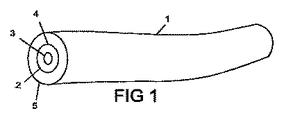
図1は、導波路2を含む光ファイバ1を示している。導波路2は、屈折率n1を具備したコア3と、屈折率n2を具備したペデスタル4と、ガラスから製造された屈折率n3を具備する第1クラッディング5と、を有する。好ましくは、n1>n2>n3である。光ファイバ1は、好ましくは、n3未満の屈折率を具備したコーティングによって被覆される。この結果、ファイバ1は、ポンプ放射を少なくとも第1クラッディング5内に結合することにより、クラッディングポンピング可能である。コーティングは、好ましくは、ポリマーである。図1に示されているものなどのペデスタルファイバを増幅器内において使用した際には、クラッディングポンピング型ファイバレーザーは、ポンプダイオードを損傷する光放射に対する耐性をあまり有していないことが判明した。好ましくは、光ファイバ1は、サイドポンピングされる。
FIG. 1 shows an
光ファイバ1は、好ましくは、フォトダークニング耐性を有する光ファイバである。「耐性」により、本発明者らは、動作の際の光ファイバ1の減衰の増大が10%を上回らないことを意味している。好ましくは、減衰の増大は、2,000時間において5%を上回らないことを要する。好ましくは、増大は、2,000時間内において1%未満であることを要する。フォトダークニングに関する計測データについては、後程詳述する。
The
光ファイバ1は、好ましくは、0.15未満の開口数を具備する。
The
以下においては、シリカ、燐酸塩、アルミナ、及び酸化ゲルマニウムなどの材料を頻繁に参照している。シリカとは、純粋なシリカ、ドーピングされたシリカ、並びに、高度にドーピングされたシリカガラスを意味し、これらのガラスは、しばしば、シリケート又はシリシックガラスと呼ばれる。燐酸塩とは、五酸化燐(P2O5)などの燐の酸化物を意味している。アルミナとは、Al2O3などのアルミニウム(aluminum)の酸化物を意味している(欧州においては、「アルミニウム(aluminium)」と呼ばれる)。酸化ゲルマニウムとは、ゲルマニウムの酸化物、特にGeO2を意味している。イッテルビウムとは、酸化物としてガラス内に含まれたイッテルビウムを意味しており、且つ、ppmを単位とする濃度は、イッテルビウムイオン、特にYb3+の濃度である。同様に、(ツリウム、エルビウムなどの)その他の希土類金属と称することにより、酸化物としてガラス内に含まれた希土類金属を意味しており、且つ、ppmを単位とする濃度は、希土類金属のイオン濃度である。 In the following, reference is frequently made to materials such as silica, phosphate, alumina, and germanium oxide. By silica is meant pure silica, doped silica, as well as highly doped silica glasses, these glasses are often referred to as silicate or silicic glasses. Phosphate means a phosphorus oxide such as phosphorus pentoxide (P 2 O 5 ). Alumina means an aluminum oxide such as Al 2 O 3 (referred to in Europe as “aluminum”). Germanium oxide means germanium oxide, especially GeO 2 . Ytterbium means ytterbium contained in the glass as an oxide, and the concentration in ppm is the concentration of ytterbium ions, particularly Yb 3+ . Similarly, by referring to other rare earth metals (thulium, erbium, etc.), it means a rare earth metal contained in the glass as an oxide, and the concentration in units of ppm is an ion of the rare earth metal. Concentration.
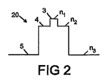
図2は、ファイバ1の屈折率プロファイル20を示している。コア3、ペデスタル4、及び第1クラッディング5の屈折率は、それぞれ、n1、n2、及びn3である。n1がn2より大きく、且つ、n2がn3より大きいことが好ましい。
FIG. 2 shows the
好適な実施例は、約0.3〜0.8モルパーセントの濃度のアルミナと、実質的に15モルパーセントの濃度の燐酸塩と、を有するシリカガラスを有するコア3を具備する。ツリウムドーパントは実質的にゼロであることが好ましい。ペデスタル4は、シリカ、燐酸塩、及び酸化ゲルマニウムを有することが好ましい。第1クラッディング5は、純粋なシリカ、フッ素ドーピングされたシリカ、又は光ファイバを製造する際に使用されるその他のクラッディング材料(ポリマーを含む)であってよい。第1クラッディング5がガラスである場合には、ファイバ1は、好ましくは、ポンプ光を増幅器及びレーザー内において導波するべく、第1クラッディング5の屈折率を下回る屈折率を具備し得るポリマーによってコーティングされる。ファイバレーザー及び増幅器内の利得媒質としてのアプリケーションの場合には、コア3及びペデスタル4の少なくとも1つのものは、希土類ドーパントによってドーピングされる。希土類ドーパントは、その濃度が、好ましくは、実質的に20000〜45000ppmの範囲にあるイッテルビウムであってよい。
A preferred embodiment comprises a
耐フォトダークニング型ファイバを使用する利点は、光ファイバ1が、高ポンピング及び反転状態、並びに、高強度下において光放射を伝播させる能力を有するという点にある。低開口数は、所謂ラージモードエリアファイバとなるように、ファイバ1を構成し得ることを意味しており、これにより、高ポンピング及び反転状態との組み合わせにおいて、ファイバレーザー及び増幅器の出力パワー及び/又は製品寿命を増大可能である。大きなモードエリアファイバの設計は、米国特許第6,614,975号に記述されている。ファイバレーザー及び増幅器の設計における更なる利点は、光ファイバがその透過率品質を製品寿命にわたって維持するため、必要とされるポンプダイオードが相対的に少ないという点にある。
The advantage of using a photodarkening type fiber is that the
前述の図面は、好適な実施例を表しているが、コア3は、0.1〜4モルパーセントの範囲の濃度のアルミナ及び2〜20モルパーセントの範囲の濃度の燐酸塩と共に、シリカを有することができる。アルミナドーピングされたコアは、酸化ゲルマニウム燐ドーピングされたペデスタルとの組み合わせにおいて、従来技術と比較し、改善された再現性を有する低開口数ファイバの製造を可能にする。0.06〜0.1、又は、好ましくは、約0.08という小さな開口数を容易に実現可能である。
Although the preceding figures represent a preferred embodiment, the
ペデスタル4は、シリカ、燐酸塩、及び酸化ゲルマニウムを有することができる。燐酸塩及び酸化ゲルマニウムの濃度は、所望の開口数を実現するべく選択される。酸化ゲルマニウムの包含は、光ファイバ製造プロセスにおいて、ペデスタル4の仮想温度(fictive temperature)を増大させ、且つ、これにより、真円度及びペデスタル4に対するコア3の同軸性の両方と、従って、第1クラッディング5に対するコア3の同軸性の保持を支援するという利点を具備する。コアの同軸性は、低損失融着接続の生成において重要である。
The
好ましくは、コア3内には、実質的にゼロのツリウムドーパントが存在する。ツリウムドーパントを除去することの重要性は、ツリウムドーパントを含むファイバは、特にフォトダークニングの影響を受け易いことが判明していることから、ファイバレーザー及び増幅器の設計において重要である。従って、わずかな少ない量のツリウムを具備した希土類ドーパントを使用することが重要である。ツリウムの濃度は、約10ppm未満、好ましくは、1ppm未満であることを要する。
Preferably, substantially zero thulium dopant is present in the
光ファイバ1は、コア3及びペデスタル4の少なくとも1つのものの内部に配置された少なくとも1つの希土類ドーパントによってドーピング可能である。希土類ドーパントは、2000〜60000ppmの範囲の濃度を具備したイッテルビウムであってよい。イッテルビウムの濃度は、約15000〜50000ppmであってよい。イッテルビウムの濃度は、好ましくは、約20000〜45000ppmである。
The
コア3内の燐酸塩の濃度は、約12〜17モルパーセントであってよい。コア3内の燐酸塩の濃度は、好ましくは、約15モルパーセントである。
The concentration of phosphate in the
アルミナの濃度は、約0.20〜1モルパーセントであってよい。アルミナの濃度は、好ましくは、約0.3〜0.8モルパーセントである。 The concentration of alumina may be about 0.20 to 1 mole percent. The concentration of alumina is preferably about 0.3 to 0.8 mole percent.
光ファイバ1は、化学気相蒸着法及び溶液ドーピング法を使用して製造可能である。技法については、米国特許第4,787,927号、第4,815,079号、第4,826,288号、第5,047,076号、及び第5,151,117号に記述されている。
The
導波路2は、信号波長においてマルチモード導波路であってよい。導波路2は、大きな長さにわたって、大きな歪及び/又はモード結合を伴うことなしに、シングルモード光を伝播させるべく構成し得る。このような設計は、高パワーファイバレーザー及び増幅器の設計において、特に、分光法、産業用の材料加工、レーザー手術、及び航空宇宙アプリケーションにおいて、重要である。コア設計、シングルモード光を伝播させる技法、並びに、望ましくない高次モードを(少なくとも部分的に)除去するための曲げ損失の使用法の例については、米国特許第5,818,630号、第6,496,301号、第6,614,975号、及び第6,954,575号に記述されている。
The
導波路2は、シングルモード導波路であってよい。
The
図3は、コア3内に複屈折性を誘発するストレス生成領域31を含む光ファイバ30を示している。コア3は、円形又は楕円形であってよい。或いは、この代わりに、又はこれに加えて、複屈折性は、ペデスタル4及びコア3の少なくとも1つのものを楕円形に製造することによって誘発させることも可能である。図14は、複屈折性を誘発する楕円形のペデスタル4を具備した光ファイバ140を示している。又、光ファイバ140は、ペデスタル4のものよりも高い粘度を具備するべく設計された内部クラッディング141をも含む。これは、例えば、その屈折率を低下させるべく、ペデスタル4内に硼素ドーパントを包含することによって実現可能である。このような複屈折ファイバを製造する技法については、米国特許第4,274,854号及び第4,426,129号に記述されている。このようなファイバにおいては、楕円形ジャケット内にペデスタルを整形することができるように、ペデスタル内の酸化ゲルマニウムのドーパント濃度を低減又は除去することが有利であることに留意されたい。或いは、この代わりに、又はこれに加えて、前述の特許番号によって開示されているように、楕円形ジャケットを形成するべく、硼素の酸化物によってドーピングされた追加のクラッディング(図示されてはいない)をファイバ1に包含することも可能である。又、光ファイバ30及び140は、米国特許第6,496,302号及び同時係属中の本明細書と同一の譲受人に譲渡された米国特許出願第10/528,895号に記述された、シングルモード又はマルチモードであり得る単一偏光光ファイバであってもよい。
FIG. 3 shows an
図4は、ポンプ44と、光ファイバ41と、を有するクラッディングポンピング型増幅光学装置40の形の装置を示している。光ファイバ41は、光ファイバ1、30、又は140であってよい。クラッディングポンピング型光学装置40は、共通コーティング46内に、光ファイバ41と、ポンプファイバ43と、を有する複合ファイバ42を利用している。複合ファイバ42については、米国特許第6,826,335号に記述されている。米国特許第4,815,079号、第5,854,865号、第5,864,644号、及び第6,731,837号に記述されたものなどのその他のクラッディングポンピング型ファイバ及び構成も可能である。低開口数のコア3から散乱又は漏洩する信号光は、ペデスタル4により、優先的に捕獲及び導波され、この結果、ポンプ44に返送されないため、本発明は、特に有利である。従って、本装置は、クラッディングポンピング型レーザーの主要な障害メカニズムの1つのものを、即ち、望ましくない信号光によって生じるポンプダイオードの破滅的な障害を除去する。クラッディングポンピング型光学装置40は、増幅器、レーザー、主発振器パワーアンプ、Qスイッチレーザー、或いは、少なくとも1つのポンプエネルギーの供給源を有する超高速レーザーであってよい。超高速レーザーとは、例えば、1nm未満の、更に好ましくは、10ps未満のパルス幅を具備したパルスを放射する、モードロックされたレーザー及び/又は主発振器パワーアンプの形のレーザーを含むレーザーを意味している。超高速レーザーの設計及びアプリケーションについては、米国特許第6,885,683号、第6,275,512号、第5,627,848号、第5,696,782号に開示されている。
FIG. 4 shows a device in the form of a cladding pumping amplification
図5は、材料加工用のレーザー50の形の装置を示している。レーザー50は、増幅光学装置40、レーザー供給ファイバ51、及び加工ヘッド52を有する。加工ヘッド52は、スキャナ、ガルバノメーター、又は合焦レンズであってよい。レーザー50は、金属、プラスチック、及びその他の材料のマーキング、微細溶接、印刷、微細機械加工、及び切断に特に有用である。
FIG. 5 shows an apparatus in the form of a
図6は、それぞれが、イッテルビウム、アルミナ、酸化ゲルマニウム、及び硼素の酸化物によってドーピングされたコア3を有する、4つの連続波ファイバレーザー内におけるフォトダークニングの効果を示している。この図は、4つの異なるファイバレーザーにおける時間66に伴う出力パワー61の計測値を示している。これらのファイバレーザーのそれぞれのコア3は、標準的な市販品のイッテルビウムドーパントによってドーピングされた。ライン62は、高いツリウム含有量を具備した標準的な市販のイッテルビウムドーパントによってドーピングされた、ファイバレーザーからの計測値を示している。出力パワー61の迅速な減少が観察される。ライン63は、60Wの連続波出力パワーを出力するファイバレーザーから30℃において採取された計測値を示している。ファイバコア1は、標準的な市販のイッテルビウムによってドーピングされた。この場合にも、観察可能な出力パワー61の迅速な減少が存在する。ライン64は、110Wの連続波出力パワーを出力するファイバレーザーから70℃において採取された計測値を示している。最後に、ライン65は、60Wの連続波出力パワーを出力するファイバレーザーから30℃において採取された計測値を示している。イッテルビウムドーパントは、高純度であり、百万分の1未満の規定の不純物レベルを有する。イッテルビウムドーパントは、高純度であり、百万分の1(1ppm)未満の規定の不純物レベルを有する。ライン63及び65を比較することにより、高純度イッテルビウムの使用は、同一レベルの出力パワー及び温度において計測された際のフォトダークニングの効果を低減している。ライン64をライン65と比較することにより、30℃から70℃への温度の上昇は、フォトダークニングの増大を引き起こしている。非常に低レベルのツリウム及びその他の不純物を有するYbドーパントを利用することによって実現されたフォトダークニングに対する耐性の大きな改善が、明らかに存在する。残りのフォトダークニング効果は、その他の屈折率制御コアコドーパント、即ち、アルミナ、酸化ゲルマニウム、及び硼素の酸化物に起因すると考えられる。
FIG. 6 shows the effect of photodarkening in four continuous wave fiber lasers, each having a
Kitabayashi他は、Proceedings of Optical Fiber Communications 2006 Conferenceにおいて発表された「Population inversion factor dependence of photodarkening of Yb−doped fibers and its suppression by highly aluminum doping」という名称の自身の論文において、Ydドーピングされたファイバ内のフォトダークニングは、アルミニウムドーピングを包含することによって低減可能ではあるが、完全には除去することができないことを開示している。この内容は、本引用により、本明細書に包含される。 Kitabayashi others, was published in the Proceedings of Optical Fiber Communications 2006 Conference in the "Population inversion factor dependence of photodarkening of Yb-doped fibers and its suppression by highly aluminum doping" own paper entitled, Yd doped in the fiber Photodarkening discloses that it can be reduced by including aluminum doping, but cannot be completely removed. This content is hereby incorporated by reference.
驚いたことに、本発明者らは、ファイバ1のコア3から酸化ゲルマニウムを除去し、且つ、燐酸塩ドーパントを包含することにより、更なる改善を実現可能であることを発見した。図7は、アルミナドーピングされたコア1内に燐酸塩ドーパントを包含することによって得られた改善を示している。コア1は、酸化ゲルマニウム及び硼素ドーピングを含んでいない。コア1は、ツリウム及びその他の希土類に起因した汚染を最小限に維持するべく、イッテルビウムの高純度の酸化物(1ppmよりも良好になるように規定された合計不純物含有量)によってドーピングされた。曲線67は、アルミナドーパントを有する結果を示しており、曲線68は、アルミナ及び燐酸塩ドーパントを有する結果を示している。Kitabayashi他の結果によれば、アルミナは、単独では、フォトダークニング効果を完全に抑圧することができないとされている。しかしながら、本発明者らは、アルミナに加えて燐酸塩コドーパント(co−dopant)を包含することにより、結果的に劇的な改善がもたらされ、この結果、イッテルビウムドーピングされたファイバ内のフォトダークニング効果が劇的に低減されることを発見した。又、重要なことは、コア内におけるアルミナドーパントの使用は、燐酸塩ドーピングのみによるものよりも高い再現性を有する低開口数の導波路の製造をも可能にすることである。
Surprisingly, the inventors have found that further improvements can be realized by removing germanium oxide from the
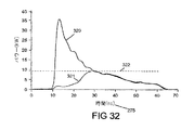
又、光ファイバのフォトダークニングは、加速エージング試験に晒された状態において、光ファイバの(対象である1ミクロン領域の周囲の)吸収の増大を監視することにより、特徴付けすることも可能である。エージングは、イッテルビウムドーピングされたコアをポンピングして可能な最大反転を実現することにより、加速される。図8〜図10を参照して示された計測値は、976nmにおける約400mWのポンプ光によって長さが約0.1〜1mのファイバをコアポンピングし、且つ、タングステンフィラメントからの白色光をコア内に結合することにより、得られた。次いで、スペクトル吸収をカットバック計測によって計測した。計測法は、L.L. Koponen他による「Photodarkening in ytterbium−doped silica fibers」(Proceedings of SPIE Volume 5990)という論文に発表された方法に準拠しており、この内容は、本引用により、本明細書に包含される。損失81対波長83の計測値を加速エージングの前及び後において採取した。図8は、そのコアが高純度のYb、酸化ゲルマニウム、及び硼素によってドーピングされたファイバレーザー内における加速エージングの前84及び後85における損失81の計測値を示している。図9は、市販の耐フォトダークニング型Ybドーピングファイバを使用した同一の計測値を示している。図10は、図1に示されたファイバ1を含むファイバレーザーに関する同一の計測値を示している。図8〜図10のそれぞれのものにおいて、約850〜1050nmのイッテルビウムの吸収ピークが明らかである。この理由から、(図8及び図9の)曲線86及び87により、且つ、図10の曲線101により、減衰曲線84及び85を外挿した(曲線84及び85の間に識別可能な差が存在しないため)。フォトダークニングは、波長83の減少に伴って増大する損失81の増大により、図8において明らかである。対象の領域88は、1000nm〜1100nmにおける損失81の増大を示す、図8及び図9のハッチングエリアによって示されている。図9に対応するファイバは、図8に対応するファイバよりも、格段に小さな損失の増大を明らかに示している。しかしながら、図10から明らかなように、強調表示されたエリア102によって明白に示されているように、この波長帯域には、明らかなフォトダークニングは存在していない。従って、本発明のこの態様によるファイバ設計は、フォトダークニングを除去している。
Optical fiber photodarkening can also be characterized by monitoring the increase in absorption (around the 1 micron region of interest) of the optical fiber when exposed to accelerated aging tests. is there. Aging is accelerated by pumping the ytterbium-doped core to achieve the maximum possible reversal. The measured values shown with reference to FIGS. 8 to 10 are obtained by core-pumping a fiber having a length of about 0.1 to 1 m with a pump light of about 400 mW at 976 nm, and core white light from a tungsten filament. Obtained by binding in. The spectral absorption was then measured by cutback measurement. The measurement method is L.L. L. This is in accordance with a method published in the paper “Photodarkening in ytterbium-doped silica fibers” (Proceedings of SPIE Volume 5990) by Koponen et al., The contents of which are hereby incorporated by reference. Measurements of
図11及び図12は、図10の加速エージング試験において使用されたものに類似したドーパントを有する図1のファイバを利用したファイバレーザーからの出力パワー110対時間111を示している。それぞれの図中の上部計測ラインは、出力パワー110であり、下部ラインは、計測値が採取された周辺温度112である。図11に示された結果を得るべく使用されたファイバレーザーは、0.6mJのパルスエネルギー及び35nsのパルス幅を具備した20kHzのパルスを有する12Wの平均パワーを放射する主発振器パワーアンプ(図示されてはいない)であった。図12に示された結果を得るべく使用されたファイバレーザーは、ポンプ源として使用されたレーザーダイオードを10kHzにおいて且つ70%のデューテイサイクルにおいて反復的にターンオン及びオフすることにより、10kHzにおいて変調された連続波レーザーであった。高ピークパワーのパルス主発振器パワーアンプ及び連続波レーザーの両方において、2〜3ヶ月の連続運転にわたって、時間111に伴う出力パワー110の劣化が生じていないことを図11又は図12の両方において観察可能である。
FIGS. 11 and 12 show the
図13は、本発明の好適な実施例における屈折率プロファイル130を示している。プロファイル130は、崩壊(collapse)におけるドーパント(特に、燐酸塩)の蒸発に起因したコア3内の中央の落ち込み130を含むという点において、図2の理想的なプロファイルとは異なっている。コア3とペデスタル4の間の屈折率差131は、n1−n2によって付与され、これは、約0.0032である。これは、約0.096の開口数に対応する。同様に、ペデスタル4と第1クラッディング5の間の屈折率差132は、約0.0097であり、これは、約0.17の開口数に対応する。コア3は、約0.70モルパーセントのドーパント濃度を有するアルミナと、約15モルパーセントのドーパント濃度を有する燐酸塩と、約25000ppmのドーパント濃度を有するイッテルビウムと、によってドーピングされた。イッテルビウムドーパントは、1ppm未満の不純物含有量を有するイッテルビウムの酸化物によって提供され、従って、コア3内には、実質的にツリウムドーパントが含まれていなかった。ペデスタル4は、約0.0032という所望のペデスタル4に対するコア3の屈折率131を提供するのに十分なレベルにおいて、燐及びゲルマニウムによってドーピングされた。ペデスタル4内の燐酸塩は、堆積されるコア3により、プレフォームの崩壊の際に蒸発することにならないため、ペデスタルの屈折率差132は、高精度で製造可能であることに留意されたい。又、燐酸塩とは異なり、アルミナドーパントは、プレフォームの崩壊の際に蒸発の影響を相対的に受けないため、コア屈折率差131も、同様に、高精度で製造可能である。従って、好ましい実施例は、高精度において、且つ、製造の際のコア3からのドーパントの大規模な蒸発を伴うことなしに製造可能であるフォトダークニング問題に対する解決策を提供している。25000ppmというイッテルビウムのドーパント濃度は、約20000ppm〜40000ppmにおいて変化可能である。更に大きな値は、ファイバレーザー又は増幅器内におけるポンプ吸収の増大を許容する。これは、使用する活性ファイバの必要な長さを低減するという更なる利点をも具備する。5μm〜50μmの範囲の又は(非常に大きなパワーのレーザー及び増幅器に使用される場合の100μmなどの)これよりも大きな直径を有するコアを製造するべく、製造の際にプレフォームをオーバースリービングすることにより、又は当産業において既知のその他の技法により、コア3の直径133を変更可能である。コア3は、シングルモード又はマルチモードであってよく、且つ、コア3及び/又はペデスタル4に伴うドーパント濃度を調節することにより、等価な開口数が約0.06〜0.15の範囲、好ましくは、0.08〜0.15の範囲になるように、屈折率差131を変更可能である。ペデスタル4の直径134は、コア4の直径133の約1〜5倍の範囲、好ましくは、コア4の直径133の1.5〜4倍のレンジ、更に好ましくは、コア4の直径133の約2.0〜4倍であってよい。図13に示された設計は、本明細書に記述されたファイバ1、30、41、又は140のコア3及びペデスタル4の基礎として使用可能である。
FIG. 13 shows a
主発振器パワーアンプパルスレーザーの増幅の最終段内における(図13に示された)中央の落ち込みを有する活性ファイバの使用は、低パワーの前置増幅器段によって後続された半導体シードレーザーを有する主発振器パワーアンプ構成において、非常に有益であることが判明した。 The use of an active fiber with a central dip (shown in FIG. 13) in the final stage of amplification of the master oscillator power amplifier pulsed laser is a master oscillator with a semiconductor seed laser followed by a low power preamplifier stage. It has been found to be very useful in power amplifier configurations.
中央の落ち込みの存在によって生成された非ガウスモードプロファイルは、フラットトップ屈折率におけるモードとの関係において、ファイバピグテールに対する乏しい整合性を有するため、これは意外であった。信号接続損失の増大は、増幅器内において使用されたポンプパワーと出力信号パワーの間の比率として定義される増幅器効率の低減を結果的にもたらすものと考えられた。逆に、活性ファイバコア内に落ち込みを導入することにより、増幅器効率の改善が得られた。所望のレーザー出力パワーに到達するべく必要とされるポンプダイオードの数が相対的に少なくなるため、高効率は、大きな利点を提供する。 This was surprising because the non-Gaussian mode profile generated by the presence of the central dip has poor matching to the fiber pigtail in relation to the mode at the flat top refractive index. The increase in signal connection loss was thought to result in a reduction in amplifier efficiency, defined as the ratio between the pump power used in the amplifier and the output signal power. Conversely, an improvement in amplifier efficiency was obtained by introducing a dip in the active fiber core. High efficiency provides a significant advantage because the number of pump diodes required to reach the desired laser output power is relatively small.
様々な活性ファイバの特徴判定において、300mWの入力信号パワーを使用した。これは、半導体シードレーザーからの5〜10mWの平均出力パワー及び前置増幅器段における〜25dBの増幅を有する対象の主発振器パワーアンプ構成において、一般的なものである。 An input signal power of 300 mW was used in characterizing various active fibers. This is common in master oscillator power amplifier configurations of interest having an average output power of 5-10 mW from a semiconductor seed laser and ˜25 dB amplification in the preamplifier stage.
フラットトップ屈折率プロファイルを有するファイバの計測された効率は、複数の横モードが活性ファイバ内において励起された際には、50〜55%であり(マルチモード効率)、更に低次のモードが励起された際には、25〜35%と低かった(略して、シングルモード効率と呼ばれる)。良好な出力ビーム品質を目標としているため、ファイバレーザーにおいては、後者のほうが関係している。 The measured efficiency of a fiber with a flat top refractive index profile is 50-55% when multiple transverse modes are excited in the active fiber (multimode efficiency), and lower order modes are excited. When it was done, it was as low as 25-35% (abbreviated as single mode efficiency). The latter is more relevant in fiber lasers because it targets good output beam quality.
この代わりに、中央の落ち込みを有するファイバは、65〜70%のマルチモード効率を、そして、50〜55%という高いシングルモード効率を示した。コアの中央に異なる落ち込みを有する様々なファイバについて、これらの結果を得た。屈折率低下の変化は、−0.003〜−0.010の範囲であった。 Instead, a fiber with a central dip showed 65-70% multimode efficiency and a high single mode efficiency of 50-55%. These results were obtained for various fibers with different dip in the center of the core. The change in refractive index drop was in the range of -0.003 to -0.010.
これは、媒質内において入手可能な最大エネルギーに対するレーザー媒質から抽出されたエネルギーの比率として定義される、様々な設計の様々なエネルギー抽出効率を考慮することにより、説明可能である。エネルギー抽出効率は、活性媒質の入力飽和を増大させることにより、即ち、更に大きな信号入力パワーを使用するか又は活性媒質とファイバモードのオーバーラップを改善することにより、増大可能である。半導体シード+1つの前置増幅段から取得可能である相対的に低いパワーは、良好なオーバーラップを目標としなければならないことを意味している。 This can be explained by considering different energy extraction efficiencies for different designs, defined as the ratio of the energy extracted from the laser medium to the maximum energy available in the medium. The energy extraction efficiency can be increased by increasing the input saturation of the active medium, i.e. by using a larger signal input power or by improving the overlap between the active medium and the fiber mode. The relatively low power that can be obtained from the semiconductor seed plus one preamplification stage means that good overlap must be targeted.
フラットトップのファイバにおいては、相対的に低次のモードがコアの中心の周りに集中し、これにより、コアエッジの近傍における大量のYbイオン内に保存されたエネルギーの効率的な使用が妨げられる。実際に、Ybドーパントプロファイルは、Ybイオンの高いモル屈折度に起因し、コアの屈折率プロファイルに略準拠していると仮定することが妥当である。 In flat top fibers, relatively low order modes are concentrated around the center of the core, which prevents efficient use of the energy stored in the bulk of Yb ions near the core edge. In fact, it is reasonable to assume that the Yb dopant profile is largely compliant with the core refractive index profile due to the high molar refractive index of Yb ions.
逆に、相対的に低次のモードプロファイルは、中央の落ち込みを有するファイバ内のYb分布プロファイルと整合している。ドーパントのすべてのセクションが効率的に入力信号によって使用され、この結果、相対的に良好な飽和の平均レベル及び良好な抽出効率が得られる。屈折率において−0.003という小さな低下が導入された際には、大きな利点が理論的に見出されるが、低下が更に増大した場合には、変化は、無視可能である。 Conversely, the relatively low order mode profile is consistent with the Yb distribution profile in the fiber with a central dip. All sections of the dopant are efficiently used by the input signal, resulting in a relatively good average level of saturation and good extraction efficiency. A great advantage is theoretically found when a small decrease in refractive index of -0.003 is introduced, but if the decrease is further increased, the change is negligible.
更なる利益は、ファイバの製造における製造公差の緩和と(この理由は、落ち込みは、プレフォームの崩壊プロセスにおけるドーパントの蒸発に関係しており、これは、制御が困難であるためである)、中央の落ち込みが所与の出力エネルギーにおける基本のピーク強度を低下させ、これによって非線形効果が低減されるという点にある。 A further benefit is the relaxation of manufacturing tolerances in the manufacture of the fiber (because the sag is related to the evaporation of dopants in the preform collapse process, which is difficult to control), The central dip is that the fundamental peak intensity at a given output energy is reduced, thereby reducing non-linear effects.
可能な欠点は、増幅器内におけるパルス整形の増大によって付与される。相対的に良好な抽出効率は、増幅器内における相対的に不良なパルス変形と、同一の合計パルスエネルギーにおけるパルスリーディング端部のピークパワーの増大を結果的にもたらす。これは、非線形効果及びパルス形状制御の両方にとって有害である。小さな落ち込み(約0.003の屈折率の変化)により、相対的に厳格な製造要件を代償として、効率と整形の間の最適なバランスが得られる。 A possible drawback is given by the increased pulse shaping in the amplifier. A relatively good extraction efficiency results in relatively poor pulse deformation within the amplifier and an increase in peak power at the pulse leading end at the same total pulse energy. This is detrimental to both nonlinear effects and pulse shape control. A small dip (a change in refractive index of about 0.003) provides an optimal balance between efficiency and shaping at the expense of relatively stringent manufacturing requirements.
図15は、連続波200Wレーザーにおける出力パワー110対時間111を示している。200Wレーザーは、その出力が200W光ファイバ増幅器によって増幅される20Wファイバレーザーを有する。200Wファイバ増幅器は、図13に示されたものに類似した屈折率プロファイルを有するファイバを使用した。コア3は、アルミナ、燐酸塩、及びイッテルビウムによってドーピングされた。出力パワー110は、70時間において、約2W(0.7%)だけ減少した。この小さな減少は、フォトダークニング以外の理由によって発生した可能性がある。対照的に、図16は、窪んだ内部クラッディングを有する従来の屈折率ステップ型ファイバを、200Wの光学増幅器内において使用した等価的な結果を示している。コアは、アルミナ、硼素、イッテルビウムによってドーピングされた。出力パワー110は、35時間において、約25W(10%)だけ劣化したことが観察される。コア内においてアルミナ及び燐酸塩ドーパントを使用することによって得られた改善が明らかに実証されている。
FIG. 15 shows the
フォトダークニングが、mWから数百ワットのパワーレベルにおいて発生することを実証する実験結果を提示した。主要な要因は、ドーパントの組成と、実際的に可能な限り低減することを要するファイバ内における反転の量である。反転の低減は、光学増幅システムの全体を通じて、すべての段においてわずかな信号利得を低減することにより、実現可能である。フォトダークニングは、10dBを上回る光学利得において問題となり、特に、20dBを上回る光学利得において問題となる。 Experimental results have been presented that demonstrate that photodarkening occurs at power levels from mW to several hundred watts. The main factors are the dopant composition and the amount of inversion in the fiber that needs to be reduced as much as practical. Inversion reduction can be achieved by reducing the slight signal gain at all stages throughout the optical amplification system. Photodarkening becomes a problem at optical gains above 10 dB, and in particular at optical gains above 20 dB.
本明細書に記述された解決策は、1ワット未満から数千ワットのパワーレベルにおいて、連続波レーザー及び数十フェムト秒〜数百ミリ秒のパルス幅を具備するパルスレーザーにおいて、シングルモード及びマルチモード出力の両方おいて、且つ、ランダム偏光された及び偏光された出力の両方において、適用可能であると考えられる。記述された内容は、イッテルビウムドーピングに合焦しているが、本発明者らは、これらの結果は、誘導ラマン散乱(SRS)に基づいたファイバレーザー及び増幅器、並びに、ネオジミウム、イッテルビウム、エルビウム、ネオジミウム、プラセオジミウム、ツリウム、サマリウム、ホルミウム及びジスプロシウム、イッテルビウムコドーピングされたエルビウム、或いは、イッテルビウムコドーピングされたネオジミウムを含むものにも適用可能であると考える。これらの解決策は、約1350nm未満の波長において動作するファイバレーザー及び増幅器にとって重要であり、特に、1100nm未満の波長において動作するファイバレーザー及び増幅器にとって重要である。又、これらの結果は、特にファイバレーザーからの出力が800nm未満の波長を具備する際には、(図5のファイバ51などの)ビーム供給ファイバの設計にも適用可能である。これは、例えば、非線形結晶、導波路、又はファイバ、或いは、チャープされた周期的に分極されたニオブ酸リチウムなどの材料を使用し、周波数倍増又は三倍増を通じて実現可能である。解決策は、高いヒドロキシル基(OH)含有量を有するシリカ、所謂「ウェットシリカ」の使用などの、フォトダークニングを低減するための従来の方法との関連において使用可能である。これは、重水素によって充填可能であり、且つ、紫外光によって照射可能である。
The solution described herein is for single mode and multi-mode in continuous wave lasers and pulsed lasers with pulse widths of tens of femtoseconds to hundreds of milliseconds at power levels of less than 1 watt to thousands of watts. It is believed to be applicable both at mode output and at both randomly polarized and polarized output. While the described content is focused on ytterbium doping, the inventors have found that these results are based on stimulated Raman scattering (SRS) based fiber lasers and amplifiers, and neodymium, ytterbium, erbium, neodymium. It may also be applicable to those containing praseodymium, thulium, samarium, holmium and dysprosium, ytterbium co-doped erbium, or ytterbium co-doped neodymium. These solutions are important for fiber lasers and amplifiers operating at wavelengths below about 1350 nm, and in particular for fiber lasers and amplifiers operating at wavelengths below 1100 nm. These results are also applicable to the design of beam delivery fibers (such as
図17は、光源172、少なくとも1つの増幅器173、及びコントローラ174を有する光放射1713を提供する装置171を示している。光源172は、出力パルス1719を生成するべく増幅器173によって増幅される光学パルス175を放射する。出力パルス1719は、パルス繰り返し周波数176、パルス持続時間177、ピークパワー179、平均パワー178、及びパルスエネルギー1710によって特徴付けられている。パルスエネルギー1710は、パルス1719の下部のシェーディングエリアとして、図17に示されている。装置171は、増幅器173と光放射1713を材料1714に導波する任意選択の加工ヘッド1712の間に任意選択の光ファイバケーブル1711を具備する。コントローラ174は、装置171が材料1714を加工できるように、光源172及び増幅器173の少なくとも1つを制御する。図17においては、加工は、マーク1715として描かれている。光源172は、図38のシードレーザー382を有することができる。光源172は、図38の反射器384を有することができる。増幅器173は、図38の増幅器383を有することができる。
FIG. 17 shows an
又、加工は、マーキング、印刷、切断、穿孔、溶接、微細溶接、蝋付け、アニーリング、並びに、その他の材料加工アプリケーションを包含することも可能である。又、加工は、(皮膚などの)組織の治療、歯科医術、及び外科などの生物学的プロセスを包含することも可能である。 Processing can also include marking, printing, cutting, drilling, welding, fine welding, brazing, annealing, and other material processing applications. Processing can also include biological processes such as treatment of tissue (such as skin), dentistry, and surgery.
加工ヘッド1712は、光放射1713をスキャニングするスキャニングヘッド又はガルバノメーターを有することができる。或いは、この代わりに、又はこれに加えて、加工ヘッド1712は、光放射1713をコリメート及び/又は合焦する少なくとも1つのレンズを有することも可能である。好ましくは、加工ヘッド1712は、材料1714から由来する後方反射による増幅器173の不安定化を防止するべく、ハイパワー光学アイソレータを包含可能である。
The
装置171を使用して加工される材料1714は、半導体パッケージ(プラスチック又はセラミック)、携帯電話機上のキーパッド、iPOD、コンピュータ、コンポーネント、パッケージ、又は商用又は産業用の製品などの物品であってよい。
The
前置増幅器、パワー増幅器、並びに、図17の装置内において使用可能である光学構成は、反射器196を除いて、米国特許第6,433,306号に記述されており、この内容は、本引用により、本明細書に包含される。この特許が記述しているように、装置171のピークパワー179の増大に伴い、非線形効果が出現し始める。誘導ブリルアン散乱(SBS)を回避するべく提案された解決策は、増幅段が相対的にSBSから免れるように、存在する多数のモードの数だけSBS閾値を増大させるべく、複数波長を具備したレーザーダイオードを光源2として使用するというものである。本発明者らは、この方法は、約1kW〜5kW未満のピークパワー179において一般的に好適であることを見出した。しかしながら、以下において観察されるように、この解決策に基づいた主発振器パワーアンプ(MOPA)は、レーザーを損傷可能であるランダムパルシングの傾向を有する。この効果は、SBSに起因するものと考えられる。ファイバのモードエリアを増大させるなどの解決策は、SBS閾値を増大させはするが、確実に約5kW超に増大させることは困難であることが証明された。米国特許第6,433,306号は、SBS閾値を増大させるための又はランダムパルシングを回避するための反射器196の使用法を開示又は提案してはない。
Preamplifiers, power amplifiers, and optical configurations that can be used in the apparatus of FIG. 17, except for
SBSによって生じる問題の一例として、12kWのピークパワーを放射する装置内において、50を超える数のモードを具備したレーザーダイオードを使用した。(1時間〜数ヶ月などの)かなりの期間にわたって20kHzにおいて変調された際に、増幅器173を有する導波路に内部的な損傷を生成するトランジェントパルスが、出力において観察された。この効果は、時折発生するライン幅のナローイング及びこの結果としてSBSの発生をもたらす半導体レーザー内のランダム効果に起因して発生すると考えられる。この効果は、恐らくはSBSに起因すると思われるが、これは証明されてはいない。しかしながら、トランジェントパルス損傷は、特に、これがまれにしか発生しないことから、定量化すること、そして、このような装置から除去することが、非常に困難であることが判明した。
As an example of the problem caused by SBS, laser diodes with more than 50 modes were used in a device emitting 12 kW peak power. Transient pulses were observed at the output that produced internal damage to the waveguide with
驚いたことに、本発明者らは、図18の装置180を使用し、この問題を解決することができた。半導体レーザーを、スーパールミネッセントダイオード(SLED)181、アイソレータ186、及び前置増幅器182によって置換した。前置増幅器182は、ポンプ189によってポンピングされている。前置増幅器182の出力は、光学アイソレータ186を介して増幅器183に結合され、次いで、これは、別の光学アイソレータ186を介してパワー増幅器1810に結合されている。増幅器183及びパワー増幅器1810は、ポンプ184及び1811によってそれぞれポンピングされている。ポンプ189、184、及び1811は、好ましくは、半導体レーザーである。
Surprisingly, the inventors were able to solve this problem using the
半導体レーザーをSLED181によって置換することは、直観に反した方法である。これは、SLED181が、半導体レーザーよりも格段に小さなパワーを具備するためである。この結果、前置増幅器182は、飽和せず、且つ、増幅器183とパワー増幅器1810の利得を飽和させるASEをパルス1719の間に生成する。ASEは、ポンプ189が常にオンである場合に生成される。これは、ポンプ189が前置増幅器182をポンピングすることにより、反転及び後続のASEの生成をもたらすためである。パルスの間においてターンオフされ、且つ、SLED181から到来するパルスの前にターンオンされるようにポンプ189を変調することにより、ASEの効果を低減可能である。正確なタイミングは、前置増幅器182の設計と、特に、ポンプ189から入手可能であるパワーに依存しており、ポンプパワーが大きいほど、ポンプ189をターンオン状態に維持するべく必要とされる時間は少なくなる。或いは、この代わりに、又はこれに加えて、前置増幅器182とパワー増幅器1810の間に光学スイッチ1812を挿入することも可能である。好ましくは、光学スイッチ1812は、前置増幅器182と増幅器183の間に挿入される。或いは、この代わりに、又はこれに加えて、フィルタ(図示されていない)を使用し、ASEをフィルタリングすることも可能であるが、これは、ポンプを変調するか又は光学スイッチ1812を使用するほどに効率的であるとは考えられない。光学スイッチ1812は、音響光学変調器、導波路スイッチ、ケラーセル、又はポッケルスセルであってよい。
Replacing the semiconductor laser with
SLED181及びポンプ189、184、及び1811は、コントローラ25によって制御されており、このコントローラは、装着されている場合には、光学スイッチ1812をも制御することになろう。これらの装置は、同期状態となると共に非線形及び損傷効果を低減するべく、制御されることになろう。
前置増幅器182、増幅器183、及びパワー増幅器1810は、コアポンピング又はクラッディングポンピング可能である。好ましくは、前置増幅器182は、コアポンピング型の前置増幅器である。これは、コアポンピング型の前置増幅器は、相対的に短い装置であって、こちらのほうが効率的であるためである。好ましくは、増幅器183及びパワー増幅器1810は、クラッディングポンピングされる。このような構成は、低コストで製造可能な効率的な装置を提供する。
前置増幅器182、増幅器183、及びパワー増幅器1810内に含まれた光ファイバは、それぞれ、ソリッドコアファイバ又は所謂ホーリーファイバであってよい。これらは、好ましくは、イッテルビウム、エルビウム、ネオジミウム、ホルミウム、ツリウム、又はプラセオジミウムなどの希土類ドーパントによってドーピングされる。好ましくは、光ファイバは、フォトダークニングに対する耐性を有する。このようなファイバについては、図1〜図16を参照して説明されている。
The optical fibers included in the
好ましくは、SLED181は、10nmを上回る、好ましくは、20nm〜40nm、又はこれを上回る帯域幅を具備する。帯域幅が大きいほど、SBS閾値も大きく、この結果、本発明の装置の信頼性が高くなる。
Preferably, the
その他の形態の(エッジ発光LEDなどの)LEDや(格子によってフィルタリングされたASE源などの)スーパールミネッセントファイバ源などのその他の広帯域源を図17の光源172として使用し、SLED181を置換可能である。
Other broadband sources, such as other forms of LEDs (such as edge-emitting LEDs) or superluminescent fiber sources (such as ASE sources filtered by a grating) can be used as the
本発明者は、図19に示された装置を使用することにより、SBSイベントを防止可能であることを発見した。シードレーザー192は、好ましくは、シードレーザー382である。反射器196は、好ましくは、反射器384である。増幅器193は、好ましくは、増幅器383である。実験においては、装置190は、デポラライザ191、アイソレータ186、ポンプ199によってポンピングされた前置増幅器192、及びポンプ194によってポンピングされたパワー増幅器193を有していた。コントローラ174は、光源172、並びに、ポンプ199及び194を制御した。
The inventor has discovered that by using the apparatus shown in FIG. 19, an SBS event can be prevented. The
シードレーザー192は、約1060nmの中心波長において約50〜100個の縦モードを放射するシングル横モードファブリペロー半導体レーザーであった。反射器196は、約2nmの帯域幅を具備し、且つ、チャープされたファイバブラッグ格子であった。この反射率は、約4%であった。デポラライザ191は、互いに45度において接続された2つの長さの偏光保持ファイバを有していた。デポラライザ191の使用は、偏光変動によって発生する加工状態の変動を低減するべく、多くの材料加工アプリケーションにおいて好ましい(但し、すべてにおいてそうであるわけではない)。従って、シードレーザー192は、その放射の偏光を解消できるように十分な光学帯域幅を具備することが重要である。アイソレータ186は、増幅された自発放射がシードレーザー192内に反射して戻ることを防止するべく選択された市販の在庫品のアイソレータであった。前置増幅器192及びパワー増幅器193は、イッテルビウムドーピングされたクラッディングポンピング型ファイバ増幅器であった。ポンプ194、199は、1つに組み合わせられた多くのシングルエミッタ半導体レーザーダイオードを有していた。パワー増幅器193からの後方伝播光放射を監視するべく、タップカプラ197を提供した。タップカプラ197及び後方反射検出器198は、診断のために包含されたものであり、従って、最終的な装置の一部を形成する必要はない。
The
正常動作においては、シードレーザー192は、1kHz〜500kHzの周波数において10ns〜250nsのパルス175を提供するべくパルシングされる。25kHzにおいて、シードレーザーからのピークパワーは、約300mWであり、前置増幅器192からのピークパワーは、約100Wであり、且つ、パワー増幅器193からのピークパワーは、約10〜15kWである。
In normal operation, the
反射器196を使用しない場合には、装置190は、破滅的な障害を被ることが判明した。障害メカニズムは、パワー増幅器193内のイッテルビウムドーピングされた短い長さ(最大で100mm)の光ファイバが自動的に破壊されることによって特徴付けられる。短い長さのファイバは、白色パウダーに変化する。別の障害メカニズムは、障害が発生するパワー増幅器の一端における融着接続である。これらの及びその他の障害は、製造及び試験の両方において発生可能であり、但し、十分に試験済みの製品の場合にも、数ヶ月の動作の後に、発生可能である。
Without the
図20は、正常な動作において後方反射検出器198よって計測された(パワー増幅器193の出力において計測された)前方伝播パルス1719の光学パワー201及び出力パワー202を示している。出力パワー201は、光学パワー202よりも格段に大きなパワーを具備するため、光学パワー201及び202は、異なるスケールでプロットされている。出力パワー202は、第1反射203及び第2反射204を有する。第1反射203は、タップ197とパワー増幅器193の間の接続(図示されてはいない)に由来する。第2反射204は、光ファイバケーブル1711の出力からの反射に由来する。図20に示されたパルス形状は、装置190から出現するパルスの大部分を代表するものである。
FIG. 20 shows the
図21は、後方伝播パルスの2つの例211、212を示している。パルス211及び212は、以前と同様に光学パワー203及び204を有するが、更なるスパイク213及び214をも含む。これらの追加のスパイク213及び214は、まれにしか発生せず、且つ、発生及び大きさがランダムである。発生の頻度は、シードレーザー192の動作条件(温度、駆動電流、及びパルス形状など)を変更することによって変化させることができる。25kHzのパルス繰り返し周波数において、追加のスパイクは、約1計測/週末〜30,000計測/5分のレートで観察された。更には、発生のレートは、異なる又は同一の製造者によって供給された異なるシードレーザー192を使用することによっても変化可能である。後方伝播方向においては、追加のスパイク213、214が観察されたが、前方伝播パルス形状201においては、その徴候を観察不能である。スパイク213及び214は、誘導ブリルアン散乱(SBS)の徴候であると考えられる。
FIG. 21 shows two examples 211, 212 of backward propagation pulses.
図22は、前方方向において発生した正常な外観のパルス201上に重畳されたジャイアントパルスの一例221を示している。後方反射検出器198によって計測された関係するパルス222は、複雑な形状を有し、且つ、図20に示されたパルス202よりも数倍大きな規模を有する。実際に、光学パワー203及び204は、このスケールにおいては可視状態にはない。パルス222は、スパイク223、トレーリングエッジ224、及び落ち込み225を具備する。これらのデータは、後方スパイク213及び214が約100Hzにおいて発生するように、装置190をセットアップすることにより、得られた。この反復周波数において、ジャイアントパルス221及び関連するパルス222は、約1回/5分において発生することが観察された。換言すれば、ジャイアントパルス221は、後方伝播パルス213及び214よりも格段に頻度が低く、且つ、ランダムに発生する。
FIG. 22 shows an example of a
落ち込み225は、この場合にも、SBSの徴候であると考えられる。後方伝播パルス222は、SBSを介して前方伝播パルスをポンピングするべく十分なエネルギーを具備する。これが、前方伝播方向においてジャイアントパルス221を結果的にもたらし、従って、これが、後方伝播パルス222からエネルギーを抽出することにより、結果的に落ち込み225をもたらしている。前述のパルスは、いずれも、パワー増幅器193内の活性利得媒質によって更に増幅される。
The
図22を参照すれば、図示のジャイアントパルス221の振幅226は、(ジャイアントパルス221の重畳を伴うことのない)パルス201の振幅227の約2倍である。振幅226は、ランダムに変化しており、且つ、パルス201の振幅227の数倍になる可能性がある。ジャイアントパルス221の振幅は、パワー増幅器193内のファイバの光学損傷閾値を超過するべく十分なものになる可能性があり、且つ、前述のランダムで予測不能な破滅的な障害を引き起こしたのは、恐らくは、SBS伝播と関連する音波によって引き起こされた追加エネルギーと共に、これであろうと考えられる。但し、この説明は、理論に過ぎず、且つ、可能な障害メカニズムを説明するための本発明者らの試みは、本発明の範囲を制限することを意図したものではない。
Referring to FIG. 22, the
図23は、シードレーザー192からの代表的なスペクトル230を示している。中心波長231は、約1062nmであり、且つ、全体帯域幅232は、約6nmである。スペクトル230は、約0.045nmだけ離隔した約150個のレーザーライン233を有する(すべてが図示されてはいない)。スペクトル230は、パルス1719の進展に伴って変化することが観察されたレーザーライン233の3つのファミリー234、235、236を有する。具体的には、第1ファミリー234は、パルス持続時間177の第1段階において優勢であり(この間に、パルス1719はチャープする)、且つ、この後に、中央ファミリー235が、より優勢となる。
FIG. 23 shows a
図25は、図19の装置において反射器196として使用されたファイバブラッグ格子250(図示されてはいない)の設計を示している。図25は、波長253の関数としてプロットされた反射率251(左軸)及び群遅延252(右軸)を示している。群遅延252は、ゼロからオフセットされている。群遅延252は、その計測位置に依存することから、オフセットは任意である。反射率曲線251及び群遅延曲線252の両方には、非常に小さな数値を伴う演算に起因した数学的な特性を有する雑音が存在する。格子250は、約4nmの帯域幅255によってチャープされる。その中心波長254は、図24の中央ファミリー内に略アライメントされた状態において、1061nmとなるように設計された。図26は、格子250の計測反射率261を示している。中心波長262は、約1060.7nmであり、且つ、帯域幅263は、約2nmである。帯域幅263は、格子250の製造におけるデチューニング効果に起因し、設計帯域幅255未満である。これらの効果については、ファイバ格子の製造分野における当業者には既知である。このような格子を設計及び製造する技法は、米国特許第6,445,852号及び第6,072,926号に記述されており、これらの特許の内容は、本引用により、本明細書に包含される。
FIG. 25 shows the design of a fiber Bragg grating 250 (not shown) used as the
ここでは、格子250を追加する目的が、レーザーダイオード2からの放射を安定化させることではなかったことに留意されたい。放射波長をロックするべく、モードパーティション雑音を防止するべく、サイドモードの振幅を低減するべく(所謂サイドモード抑圧)、及び/又はライン幅を狭めるべく、しばしば、狭帯域格子(帯域幅が、約0.5nm未満、並びに、しばしば、約0.1nm未満)がレーザーダイオードパッケージングに内蔵されている。このようなすべての目的は、SBSを促進すると共にジャイアントパルスの発生頻度を増大させることになる(と考えられる)相対的に安定した放射を結果的にもたらす傾向を有することになり、且つ、従って、装置190の破滅的な障害を回避することにはならないであろう。
It should be noted here that the purpose of adding the grating 250 was not to stabilize the radiation from the
図24は、定位置に格子250を有する状態において計測されたレーザーダイオード2のスペクトル240を示している。中心波長214は、約1061nmである。スペクトル240は、スペクトル230の帯域幅232未満である帯域幅242を具備する。帯域幅242は、約2nmであり、これは、格子250からの光学的フィードバックによって決定される。米国特許第6,433,306号の開示内容によれば、このような帯域幅のナローイングは、SBS性能を劣化させると予想されよう。驚いたことに、格子250の使用は、後方伝播ランダムパルス213及び214の両方、並びに、関連する更にランダムな前方伝播ジャイアントパルス221をも除去した。装置190は、無障害(failure free)であることが判明した。その他のレーザーダイオードを有し、且つ、デポラライザを有する、及び有さない更なる実験は、装置190内に反射器196を包含することの有益な効果を確認した。格子250は、シングル横モードにおける少なくとも10%の光放射を具備し、且つ、1kW〜40kWの範囲のピークパワーを具備するパルスレーザーにおいて、信頼性の高い動作を提供することを示した。SBSによる問題の発生を伴うことなしに、最大で100kW又はこれを上回る更に大きなピークパワーを実現可能であると考えられる。
FIG. 24 shows the
格子250は、シードレーザー192(この場合には、レーザーダイオード)を不安定化させたと考えられる。即ち、パワー増幅器193内におけるSBS生成の条件が回避されるように、個別のレーザーライン233が拡張されるか、チャープされるか、又は変調されている。SBSの生成を回避するためのその他の方法は、光ファイバカプラを介して結合可能である部分反射ミラー又は表面、或いは、0.5nmを上回る、好ましくは、1nmを上回る、更に好ましくは、2nmを上回る帯域幅を具備した格子などの、広帯域反射器として反射器196を実装するというものであろう。格子250は、チャープされることが好ましいが、必ずしも、このようにする必要はない。チャープされた格子250は、シードレーザー192のスペクトルの広がりに更に寄与すると考えられる波長に依存した有効外部空洞長を提供することになる。チャープされた格子250は、好ましくは、その偏光軸がシードレーザー192の偏光保持ファイバピグテールの偏光軸とアライメントされた又は角度を有する状態において、偏光保持光ファイバ内に刻み込まれる。格子250は、非偏光保持ファイバ内にも同様に刻み込み可能である。又、シードレーザー192のピグテールも、必ずしも偏光保持ファイバである必要はない。反射器196は、レーザー放射をシードレーザー192の前面又は後面(図示されてはいない)内に反射するべく配置可能である。又、反射器196は、誘電体コーティングを有することも可能である。反射器196の反射率は、約0.1%〜10%であってよい。パルス213、214を伴わない結果が、34%という高い反射率において取得されたが、これらのレベルにおいては、パルス歪が観察された。好ましくは、反射率は、約2%〜6%である。正確な数値は、使用する特定のレーザーダイオードに依存することになり、且つ、実験によって見出すことが可能である。反射器196の反射率は、シードレーザー192の前面において使用された反射率を上回ることを要すると考えられる。又、シードレーザー192の帯域幅は、好ましくは、反射器196の帯域幅に匹敵するか又はこれを下回ると考えられる。これは、前述の実験には当て嵌まらず、従って、シードレーザー192の動作条件(温度及びドライブ電流)をシードレーザー192の異なるバッチについてセットアップする必要があった。或いは、この代わりに、又はこれに加えて、シードレーザー192の全体帯域幅及び放射波長の製造公差を包含するように、格子反射器196の帯域幅を増大させることも可能である。又、後方伝播パルスの完全な欠如は、高信頼性動作の確実な表れであるため、タップ197の提供が、このようなセットアップを可能にすることに留意されたい。
It is believed that the grating 250 destabilizes the seed laser 192 (in this case, a laser diode). That is, the
格子250は、シードレーザー192から40cm〜1mに配置された。性能に差は観察されなかった。従って、反射フィードバックによってシードレーザー192を安定化させるのに不十分な時間しか存在しないほどに距離が大きくない場合には、正確な位置は、重要ではないと考えられる。
The grating 250 was placed 40 cm to 1 m from the
シードレーザー192及びポンプ199及び194は、コントローラ25によって制御されている。光学パルス1719のパルス形状を制御するためのコントローラの使用法、並びに、材料加工におけるアプリケーション及び装置の使用法に関する更なる情報については、後述する。
The
前置増幅器192及びパワー増幅器193は、コアポンピング又はクラッディングポンピング可能である。前置増幅器192は、コアポンピング型前置増幅器であってよい。コアポンピング型の前置増幅器は、クラッディングポンピング型前置増幅器よりも短い装置であり、且つ、効率的である。或いは、この代わりに、前置増幅器192は、クラッディングポンピング型前置増幅器であってもよい。これは、コストを低減するために好ましい。好ましくは、パワー増幅器193は、クラッディングポンピングされる。このような構成は、低コストによって製造可能な効率的な装置を提供する。クラッディングポンピング型増幅器の設計及び構造は、米国特許第6,826,335号に記述されており、この内容は、本引用により、本明細書に包含される。
The
前置増幅器192及びパワー増幅器193内に含まれた光ファイバは、それぞれ、ソリッドコアファイバ又は所謂ホーリーファイバであってよい。これらは、好ましくは、イッテルビウム、エルビウム、ネオジミウム、ホルミウム、ツリウム、又はプラセオジミウムなどの希土類ドーパントによってドーピングされる。好ましくは、光ファイバは、フォトダークニングに対する耐性を有する。このようなファイバは、同時係属特許出願である代理人ドケット番号SO01−P20に記述されており、この内容は、本引用により、本明細書に包含される。
The optical fibers included in the
図19を使用し、図19の光源172及び増幅器173を置換可能である。後程詳述するように、コントローラ174は、パルス繰り返し周波数176の範囲にわたって材料1714を加工するべく、十分なレベルにおいて平均パワー178及びピークパワー179が維持されるように、前置増幅器192及び増幅器193をポンピングするシードレーザー192及びポンプ194を制御する。
19 can be used to replace the
図27は、それぞれ、115kHz、46kHz、30kHz、及び24kHzのパルス繰り返し数における出力パルス271、272、273、及び274対時間275を示している。シードレーザー192によって放射された対応する光学パルス175は、図28においては、それぞれ、パルス281、282、283、及び284として示されている。出力パルス271〜274及び光学パルス281〜284は、それぞれ、個々のパルスが重畳された図29及び図30に再生成されている。図31は、パルス繰り返し周波数176に伴うピークパワー179及びパルスエネルギー1710の変動を示している。ピークパワー179は、5kWを上回る状態において維持され、且つ、パルスエネルギー1710は、24kHz〜115kHzのパルス繰り返し周波数176において、0.1mJを上回る状態に維持されている。更には、平均パワー178は、パルス繰り返し周波数176とパルスエネルギー1710の積であるため、平均パワー178は、24kHz〜115kHzのパルス繰り返し周波数176において約10Wを上回ることを観察可能である。2段の増幅のみにより、100kHzを上回るパルス繰り返し周波数において0.1mJのパルスエネルギーによって5kWのピークパワーを実現可能であることを証明しているため、図27〜図31に示された結果は非常に重要である。MOPA190は、匹敵する平均出力パワー178のその他の光ファイバパルスレーザーと比較し、加工速度の増大における大きな有用性を具備することになる。
FIG. 27 shows
図32は、ポンプ194からのパワーの増大に伴うMOPA190からの出力パワー320を示している。35kWのピークパワーが、(ピークパワーの半分において計測された)約10nsのパルス幅によって実現されている。図33は、波長332に対してプロットされた状態において、パルスの光学スペクトル331を示している。シードレーザー192からのパルスの信号波長333は、約1062nmであった。パワーの大きな比率が、信号波長333よりも長い波長に存在しており、このパワーは、誘導ラマン散乱(SRS)などの非線形プロセスに起因し、波長シフトされている。図32を再度参照すれば、1070nmを上回る波長を減衰させる光学フィルタを使用し、出力パワー321を計測した。図32及び図33から、約8kWを上回る出力パワーが波長においてシフトされることが観察される。8kWの出力パワーを非線形閾値322として定義可能である。従って、材料加工のためのMOPA190の使用法は、図17の加工ヘッド1712内における広帯域オプティクスの使用を必要とする可能性がある。「広帯域オプティクス」とは、約10nmを上回る帯域幅を具備した信号波長を透過及び合焦可能であるオプティクスを意味している。これにも拘わらず、このモードにおいて動作するMOPA190は、約8kWを上回るピークパワー179を必要とする材料加工において大きな有用性を具備する。
FIG. 32 shows the
コントローラ174を使用し、ポンプ194及び199によって放射されるパワーを低減するか、又は出力パルス1719の形状を制御することにより、波長変換される出力パルス1719の比率を低減可能である。波長変換される比率を50%未満に、且つ、好ましくは、10%未満に低減可能である。実質的に出力パルス1719のいずれもが、図27〜図31を参照して実証されたものなどの広いレンジのパルス繰り返し周波数176にわたって波長変換されないことが好ましい。コントローラ174の制御機能は、(例えば、実験及び特徴判定を通じて実現される)開ループ制御により、或いは、MOPA190内の(例えば、増幅器193の入力又は出力又は別の場所における)ポイントからパワー(平均パワー又はピークパワー又は波長シフトされたパワー)の計測値を採取し、望ましい値と比較し、且つ、計測値と望ましい値の間の差を使用してコントローラ174によって提供された制御機能を変更する閉ループ制御により、実現可能である。
図34〜図37は、パルス繰り返し周波数(prf)176及びパルス幅177の変化がMOPA190内の出力パルス1719の形状に対して具備する効果を示している。4つの図は、いずれも、同一スケール上にプロットされており、出力パワーは、任意の単位においてプロットされている。コントローラ174は、平均パワー178が12Wに維持されるように、ポンプ194及び199を制御した。又、コントローラ174は、パルス繰り返し周波数176をその望ましい値に設定した。次いで、コントローラ174は、パルス幅177(即ち、それぞれのパルス1719の全体パルス幅)を変化させ、ピークパワー179を望ましい値に設定した。
34 to 37 show the effect that changes in the pulse repetition frequency (prf) 176 and the
図34は、25kHzのパルス繰り返し周波数、0.6mJのパルスエネルギー1710、及び12Wの平均パワー178によって計測された出力パワー340対時間275を示している。パルス幅343(即ち、コントローラ174によって制御される全体パルス幅)は、約200nsであった。出力パワー340は、ピークパワー341と、約35nsの半値全幅パルス幅342を具備する。
FIG. 34 shows the
図35は、それぞれ、2つの異なるパルス幅355及び356について計測された出力パワー350及び351対時間275を示している。パルス繰り返し周波数176は、50kHzであり、パルスエネルギー1710は、0.24mJであり、且つ、平均パワー178は、12Wであった。出力パワー350の半値全幅パルス幅354は、約35nsであった。ピークパワー352、353は、パルス幅355、356の増大に伴って低下する。
FIG. 35 shows the
図36は、それぞれ、3つの異なるパルス幅367、368、及び369について計測された出力パワー360、361、及び362対時間275を示している。パルス繰り返し周波数176は、100kHzであり、パルスエネルギー1710は、0.12mJであり、且つ、平均パワー178は、12Wであった。出力パワー360の半値全幅パルス幅126は、約35nsであった。ピークパワー363、364、365は、パルス幅367、368、369の増大に伴って低下する。
FIG. 36 shows
図37は、それぞれ、2つの異なるパルス幅375及び376について計測された出力パワー370及び371対時間275を示している。パルス繰り返し周波数176は、200kHzであり、パルスエネルギー1710は、0.06mJであり、且つ、平均パワー178は、12Wであった。出力370の半値全幅パルス幅374は、約20nsであった。ピークパワー372及び373は、パルス幅375及び376の増大に伴って低下する。
FIG. 37 shows the
図19の装置内のシードレーザーパルス175の形状を変化させることにより、ピークパワー179は、1Hz〜200kHzのパルス繰り返し周波数176のレンジにわたって、0.1mJを上回るパルスエネルギー1710を提供しつつ、5kWのレベルを上回る状態に維持された。ピークパワー179は、1Hz〜500kHzのパルス繰り返し周波数の範囲にわたって、0.04mJを上回るパルスエネルギー1710を提供しつつ、3kWのレベルを上回る状態に維持された。重要なことに、これらの結果は、いずれも、SBSの徴候を伴うことなしに、且つ、2つの増幅段のみにより、実現された。
By changing the shape of the
図19の装置内のシードレーザーパルス175の形状を制御し、増幅器192、193の利得を増大させ、且つ、これらの相対的な利得を制御することにより、本発明者らは、20〜25Wの平均パワー178、0.8〜1mJの範囲のパルスエネルギー1710、15〜20nsの範囲の半値全幅パルス幅374、18〜26kWの範囲のピークパワー179、1Hz〜25kHzのパルス繰り返し周波数を更に実証した。重要なことに、これらの結果も、SBSの徴候を伴うことなしに、且つ、2つの増幅段のみにより、実現された。
By controlling the shape of the
又、本発明は、前述のレーザー及びコントローラの中の1つ又は複数のものを有する材料加工装置(例えば、材料の切断、溶接、穿孔、マーキング、又は加工用のもの)の形態であってもよい。 The invention may also be in the form of a material processing apparatus (eg, for material cutting, welding, drilling, marking, or processing) having one or more of the lasers and controllers described above. Good.
添付の図面を参照した前述の本発明の実施例は、一例として付与されたものに過ぎず、且つ、性能を向上させるべく変更及び追加コンポーネントを提供可能であることを理解されたい。 It should be understood that the above-described embodiments of the present invention with reference to the accompanying drawings are given by way of example only and that modifications and additional components may be provided to improve performance.
本発明は、単一で又は任意の組み合わせにおいて採用された前述の特徴を包含する。 The present invention encompasses the aforementioned features employed singly or in any combination.
Claims (16)
・前記シードレーザーは、光学的有効走行時間とスペクトルと第2の帯域幅とによって規定される、ファブリペロー半導体レーザーであり、前記光学的有効走行時間は、光が前記シードレーザーを進行方向に伝搬する為に要する時間であり、
・前記シードレーザーは、前記反射器を介して前記増幅器に接続され、
・前記反射器は、前記シードレーザーによって放射された前記シーディング放射の中のある比率を前記シードレーザー内に反射して戻すべく構成され、且つ、
・前記増幅器は、屈折率n1を具備したコアと、屈折率n2を具備したペデスタルと、を有する光ファイバを有し、且つ、この場合に、前記光ファイバは、前記ペデスタルを取り囲む屈折率n3を具備したガラスから製造された第1クラッディングを含み、この場合に、
・n1はn2より大きく、
・n2はn3より大きく、更に、
・前記増幅器は、ポンプ放射を前記第1のクラッディング内に結合することによってクラッディングポンピングされ、
更に前記装置は、
・使用中において前記増幅器は、前記シードレーザーによってシードされた場合、1kWよりも大きなピークパワーを有するパルスを放射し、
・前記反射器からの光学的フィードバックは、前記第1の帯域幅が前記第2の帯域幅よりも小さくなるようなものであり、更に、
・前記ペデスタルは、前記コアから漏洩した光放射を導波するように適応されていることを特徴とする、装置。 An apparatus for providing optical radiation having a first bandwidth, comprising: a seed laser for providing seeding radiation; at least one amplifier for amplifying said seeding radiation; and a reflector.
The seed laser is a Fabry-Perot semiconductor laser defined by an optically effective travel time, a spectrum and a second bandwidth, wherein the optical effective travel time is such that light propagates through the seed laser in the direction of travel Is the time it takes to
The seed laser is connected to the amplifier via the reflector;
The reflector is configured to reflect a proportion of the seeding radiation emitted by the seed laser back into the seed laser; and
The amplifier has an optical fiber having a core with a refractive index n1 and a pedestal with a refractive index n2, and in this case, the optical fiber has a refractive index n3 surrounding the pedestal; A first cladding made from the glass provided, in this case,
N1 is greater than n2,
N2 is greater than n3, and
The amplifier is cladding pumped by coupling pump radiation into the first cladding;
Furthermore, the device
In use, the amplifier emits a pulse having a peak power greater than 1 kW when seeded by the seed laser;
The optical feedback from the reflector is such that the first bandwidth is less than the second bandwidth;
The device is characterized in that the pedestal is adapted to guide light radiation leaked from the core;
・前記コアは、シリカ、約0.1〜4モルパーセントの濃度のアルミナ、2〜20モルパーセントの濃度の燐酸塩、2000〜60000ppmの濃度のイッテルビウムを有し、且つ、
・前記ペデスタルは、シリカ、燐酸塩、及び酸化ゲルマニウムを有し、前記光ファイバは、976nmにおける約400mWのポンプ光によって長さが0.1〜1mの光ファイバをコアポンピングする場合、1000nm〜1100nmの波長において2000時間で5%以下の減衰における増加によって特徴付けられるフォトダークニング耐性の光ファイバである、装置。 12. The apparatus according to any one of claims 1 to 11, wherein the optical fiber comprises a waveguide having a numerical aperture of less than 0.15.
The core comprises silica, alumina at a concentration of about 0.1 to 4 mole percent, phosphate at a concentration of 2 to 20 mole percent, ytterbium at a concentration of 2000 to 60000 ppm, and
The pedestal comprises silica, phosphate, and germanium oxide, and the optical fiber is core-pumped from 0.1 nm to 1 m in length with about 400 mW pump light at 976 nm; A device that is a photodarkening-resistant optical fiber characterized by an increase in attenuation of less than 5% at 2000 hours at a wavelength of 1100 nm.
Applications Claiming Priority (9)
| Application Number | Priority Date | Filing Date | Title |
|---|---|---|---|
| US79945606P | 2006-05-11 | 2006-05-11 | |
| US60/799,456 | 2006-05-11 | ||
| US81216406P | 2006-06-09 | 2006-06-09 | |
| US60/812,164 | 2006-06-09 | ||
| US81943906P | 2006-07-07 | 2006-07-07 | |
| US60/819,439 | 2006-07-07 | ||
| US83497406P | 2006-07-31 | 2006-07-31 | |
| US60/834,974 | 2006-07-31 | ||
| PCT/GB2007/001707 WO2007132182A2 (en) | 2006-05-11 | 2007-05-10 | Apparatus for providing optical radiation |
Related Child Applications (1)
| Application Number | Title | Priority Date | Filing Date |
|---|---|---|---|
| JP2014012311A Division JP2014112705A (en) | 2006-05-11 | 2014-01-27 | Apparatus for providing optical radiation |
Publications (3)
| Publication Number | Publication Date |
|---|---|
| JP2009536785A JP2009536785A (en) | 2009-10-15 |
| JP2009536785A5 JP2009536785A5 (en) | 2010-07-08 |
| JP5467864B2 true JP5467864B2 (en) | 2014-04-09 |
Family
ID=38694261
Family Applications (2)
| Application Number | Title | Priority Date | Filing Date |
|---|---|---|---|
| JP2009508486A Active JP5467864B2 (en) | 2006-05-11 | 2007-05-10 | Device for providing light radiation |
| JP2014012311A Pending JP2014112705A (en) | 2006-05-11 | 2014-01-27 | Apparatus for providing optical radiation |
Family Applications After (1)
| Application Number | Title | Priority Date | Filing Date |
|---|---|---|---|
| JP2014012311A Pending JP2014112705A (en) | 2006-05-11 | 2014-01-27 | Apparatus for providing optical radiation |
Country Status (7)
| Country | Link |
|---|---|
| US (3) | US7936796B2 (en) |
| EP (2) | EP2763247A3 (en) |
| JP (2) | JP5467864B2 (en) |
| KR (1) | KR101383197B1 (en) |
| CN (2) | CN102157887B (en) |
| CA (1) | CA2652006C (en) |
| WO (1) | WO2007132182A2 (en) |
Families Citing this family (36)
| Publication number | Priority date | Publication date | Assignee | Title |
|---|---|---|---|---|
| EP2763247A3 (en) * | 2006-05-11 | 2014-09-17 | SPI Lasers UK Limited | Apparatus for providing optical radiation |
| GB2444091A (en) * | 2006-11-24 | 2008-05-28 | Gsi Group Ltd | A Laser Amplifier |
| US7450813B2 (en) | 2006-09-20 | 2008-11-11 | Imra America, Inc. | Rare earth doped and large effective area optical fibers for fiber lasers and amplifiers |
| US8055115B2 (en) * | 2007-07-05 | 2011-11-08 | Coractive High-Tech Inc. | Optically active glass and optical fiber with reduced photodarkening and method for reducing photodarkening |
| CN101796697A (en) * | 2007-07-16 | 2010-08-04 | 科拉克蒂夫高科技公司 | Luminescent device with phosphosilicate glass |
| JP2009290203A (en) * | 2008-04-30 | 2009-12-10 | Sumitomo Electric Ind Ltd | Optical amplification module and laser light source device |
| WO2010016287A1 (en) * | 2008-08-04 | 2010-02-11 | 株式会社フジクラ | Ytterbium-doped optical fiber, fiber laser and fiber amplifier |
| FR2935554B1 (en) * | 2008-09-02 | 2012-04-13 | Centre Nat Rech Scient | HIGH POWER FIBER LASER DEVICE |
| JP5415553B2 (en) * | 2008-11-28 | 2014-02-12 | エヌケイティー フォトニクス アクティーゼルスカブ | Improved clad pump optical waveguide |
| WO2010065788A1 (en) | 2008-12-04 | 2010-06-10 | Imra America, Inc. | Highly rare-earth-doped optical fibers for fiber lasers and amplifiers |
| JP5405904B2 (en) * | 2009-05-28 | 2014-02-05 | 株式会社メガオプト | MOPA light source |
| US8526472B2 (en) | 2009-09-03 | 2013-09-03 | Axsun Technologies, Inc. | ASE swept source with self-tracking filter for OCT medical imaging |
| US8670129B2 (en) | 2009-09-03 | 2014-03-11 | Axsun Technologies, Inc. | Filtered ASE swept source for OCT medical imaging |
| US8934509B2 (en) * | 2009-11-23 | 2015-01-13 | Lockheed Martin Corporation | Q-switched oscillator seed-source for MOPA laser illuminator method and apparatus |
| JP5324417B2 (en) * | 2009-12-25 | 2013-10-23 | 旭化成エレクトロニクス株式会社 | Driver for driving, amplifier for driving and information equipment |
| JP5984813B2 (en) * | 2010-09-02 | 2016-09-06 | オーエフエス ファイテル,エルエルシー | Low noise laser cavity |
| JP6002453B2 (en) * | 2012-06-06 | 2016-10-05 | 三菱電線工業株式会社 | Rare earth doped double clad fiber |
| JP6037711B2 (en) * | 2012-08-08 | 2016-12-07 | 株式会社フジクラ | Fiber laser equipment |
| JP2014059294A (en) * | 2012-08-21 | 2014-04-03 | Canon Inc | X-ray waveguide and x-ray measurement system |
| US8970935B2 (en) | 2012-09-27 | 2015-03-03 | The Johns Hopkins University | High energy fiber laser modulator |
| JP6077263B2 (en) * | 2012-10-16 | 2017-02-08 | 古河電気工業株式会社 | Laser equipment |
| JP6090780B2 (en) * | 2013-01-24 | 2017-03-08 | 国立研究開発法人産業技術総合研究所 | High power incoherent light generator |
| CN105119134A (en) * | 2014-03-13 | 2015-12-02 | 恩耐激光技术有限公司 | Algorithms for rapid gating of seed suspendable pulsed fiber laser amplifiers |
| CN105281186B (en) * | 2015-11-19 | 2018-06-22 | 北京工业大学 | Side two directional pump fusion coupler and preparation method thereof |
| GB201521214D0 (en) * | 2015-12-01 | 2016-01-13 | Spi Lasers Uk Ltd | Apparatus for providing optical radiation |
| US10033148B2 (en) | 2016-02-04 | 2018-07-24 | Lawrence Livermore National Security, Llc | Waveguide design for line selection in fiber lasers and amplifiers |
| US10348050B2 (en) | 2016-02-04 | 2019-07-09 | Lawrence Livermore National Security, Llc | Nd3+fiber laser and amplifier |
| US10490969B2 (en) * | 2016-07-15 | 2019-11-26 | Fraunhofer-Gesellschaft Zur Foerderung Der Angewandten Forschung E. V. | Active stabilization of mode instabilities in optical waveguides |
| US9985414B1 (en) | 2017-06-16 | 2018-05-29 | Banner Engineering Corp. | Open-loop laser power-regulation |
| WO2019002229A2 (en) * | 2017-06-25 | 2019-01-03 | Abacus Laser Gmbh | Laser arrangement and method for operating a laser arrangement |
| GB201719629D0 (en) * | 2017-11-24 | 2018-01-10 | Spi Lasers Uk Ltd | Apparatus for providing optical radiation |
| CN109570148A (en) * | 2018-11-08 | 2019-04-05 | 中国科学院半导体研究所 | The laser cleaning all-in-one machine of direct-connected air compressor machine |
| GB201903633D0 (en) * | 2019-03-15 | 2019-05-01 | Spi Lasers Uk Ltd | Apparatus for providing optical radiation |
| EP3869636B1 (en) * | 2020-02-21 | 2024-03-13 | Toyota Jidosha Kabushiki Kaisha | Amplification fiber and laser beam emitting apparatus |
| JP7414744B2 (en) | 2020-02-21 | 2024-01-16 | トヨタ自動車株式会社 | Amplifying fiber and laser beam emitting device |
| US11609116B2 (en) | 2020-08-27 | 2023-03-21 | Banner Engineering Corp | Open-loop photodiode gain regulation |
Family Cites Families (59)
| Publication number | Priority date | Publication date | Assignee | Title |
|---|---|---|---|---|
| US4274854A (en) | 1978-01-13 | 1981-06-23 | Bell Telephone Laboratories, Incorporated | Polarization-preserving optical fiber |
| DE3176131D1 (en) | 1980-01-11 | 1987-05-27 | Hitachi Ltd | Method of producing a preform rod for an optical fiber |
| WO1987001110A1 (en) | 1985-08-13 | 1987-02-26 | Simon Blanchette Poole | Fabrication of optical fibres |
| US4826288A (en) | 1987-04-09 | 1989-05-02 | Polaroid Corporation, Patent Department | Method for fabricating optical fibers having cores with high rare earth content |
| US4815079A (en) | 1987-12-17 | 1989-03-21 | Polaroid Corporation | Optical fiber lasers and amplifiers |
| JPH0662311B2 (en) | 1988-12-07 | 1994-08-17 | シツプ‐ソシエタ・イタリアーナ・ペル・レセルチツイオ・デル・テレコミニカイオーニ・ピー・アー | Method for doping the core of silica-based fiber preforms |
| GB9010943D0 (en) | 1990-05-16 | 1990-07-04 | British Telecomm | Wave-guiding structure with lasing properties |
| US5260823A (en) * | 1990-05-21 | 1993-11-09 | University Of Southampton | Erbium-doped fibre amplifier with shaped spectral gain |
| US5115338A (en) * | 1990-05-30 | 1992-05-19 | At&T Bell Laboratories | Multi-stage optical amplifier |
| US5225925A (en) * | 1991-01-23 | 1993-07-06 | Amoco Corporation | Sensitized erbium fiber optical amplifier and source |
| US5516784A (en) * | 1991-08-13 | 1996-05-14 | Schering Corporation | Anti-HIV (AIDS) agents |
| US5659559A (en) * | 1994-06-28 | 1997-08-19 | Sdl, Inc. | Apparatus for generating a stabilized laser source |
| US5530709A (en) * | 1994-09-06 | 1996-06-25 | Sdl, Inc. | Double-clad upconversion fiber laser |
| JP3379052B2 (en) * | 1994-09-26 | 2003-02-17 | 富士通株式会社 | WDM optical amplifier, WDM transmission system, and WDM transmission method |
| GB9509874D0 (en) | 1995-05-16 | 1995-07-12 | Univ Southampton | Optical waveguide grating |
| US5696782A (en) | 1995-05-19 | 1997-12-09 | Imra America, Inc. | High power fiber chirped pulse amplification systems based on cladding pumped rare-earth doped fibers |
| US5627848A (en) | 1995-09-05 | 1997-05-06 | Imra America, Inc. | Apparatus for producing femtosecond and picosecond pulses from modelocked fiber lasers cladding pumped with broad area diode laser arrays |
| US5701319A (en) * | 1995-10-20 | 1997-12-23 | Imra America, Inc. | Method and apparatus for generating ultrashort pulses with adjustable repetition rates from passively modelocked fiber lasers |
| US5854865A (en) | 1995-12-07 | 1998-12-29 | The United States Of America As Represented By The Secretary Of The Navy | Method and apparatus for side pumping an optical fiber |
| JPH10221656A (en) * | 1997-02-06 | 1998-08-21 | Nec Corp | Optical transmitter and optical transmitting method |
| US6151338A (en) * | 1997-02-19 | 2000-11-21 | Sdl, Inc. | High power laser optical amplifier system |
| US5892615A (en) * | 1997-03-17 | 1999-04-06 | Sdl, Inc. | Output power enhancement in optical fiber lasers |
| US6181463B1 (en) * | 1997-03-21 | 2001-01-30 | Imra America, Inc. | Quasi-phase-matched parametric chirped pulse amplification systems |
| EP2648039A3 (en) * | 1997-03-21 | 2014-07-09 | Imra America, Inc. | High energy optical fiber amplifier for picosecond-nanosecond pulses for advanced material processing applications |
| US5818630A (en) | 1997-06-25 | 1998-10-06 | Imra America, Inc. | Single-mode amplifiers and compressors based on multi-mode fibers |
| US5864644A (en) | 1997-07-21 | 1999-01-26 | Lucent Technologies Inc. | Tapered fiber bundles for coupling light into and out of cladding-pumped fiber devices |
| US5937134A (en) * | 1997-08-07 | 1999-08-10 | Lucent Technologies Inc. | Cladding pumped fiber lasers |
| US6154598A (en) * | 1997-12-22 | 2000-11-28 | Polaroid Corporation | Laser composition for preventing photo-induced damage |
| JP4011175B2 (en) * | 1998-02-06 | 2007-11-21 | 浜松ホトニクス株式会社 | Optical fiber laser apparatus and laser processing apparatus |
| JP3097662B2 (en) * | 1998-06-08 | 2000-10-10 | 日本電気株式会社 | Optical fiber amplifier |
| GB9814526D0 (en) | 1998-07-03 | 1998-09-02 | Univ Southampton | Optical fibre and optical fibre device |
| US6275512B1 (en) | 1998-11-25 | 2001-08-14 | Imra America, Inc. | Mode-locked multimode fiber laser pulse source |
| US6525872B1 (en) * | 1999-02-11 | 2003-02-25 | Jds Uniphase Corporation | Fiber grating-stabilized, semiconductor pump source |
| CA2371100C (en) | 1999-04-30 | 2012-10-02 | University Of Southampton | An optical fibre arrangement |
| DE19961132C1 (en) | 1999-12-17 | 2001-06-28 | Siemens Ag | Time/space switch with multiple functionality can implement all necessary functions for network of from very small to very large coupling capacity |
| US6340806B1 (en) * | 1999-12-28 | 2002-01-22 | General Scanning Inc. | Energy-efficient method and system for processing target material using an amplified, wavelength-shifted pulse train |
| US6496301B1 (en) | 2000-03-10 | 2002-12-17 | The United States Of America As Represented By The Secretary Of The Navy | Helical fiber amplifier |
| JP2001257422A (en) * | 2000-03-10 | 2001-09-21 | Sumitomo Electric Ind Ltd | Semiconductor laser module |
| JP2001326404A (en) * | 2000-05-16 | 2001-11-22 | Fujikura Ltd | Rare earth element doped optical fiber |
| US6584246B1 (en) * | 2000-07-05 | 2003-06-24 | Litton Systems, Inc. | Source, system and method for generating amplified stimulated emission using a coupler mechanism |
| JP4531941B2 (en) * | 2000-07-14 | 2010-08-25 | 古河電気工業株式会社 | Optical fiber for optical amplification |
| US6445852B1 (en) | 2000-08-01 | 2002-09-03 | University Of Southampton | Optical fiber grating |
| US6636347B1 (en) * | 2000-11-08 | 2003-10-21 | Corning Incorporated | Phosphorus-silicate fibers suitable for extended band amplification |
| US6608951B1 (en) | 2000-11-28 | 2003-08-19 | Lew Goldberg | Optical fiber amplifiers and lasers and optical pumping device therefor |
| DE10059314B4 (en) * | 2000-11-29 | 2018-08-02 | Tesat-Spacecom Gmbh & Co.Kg | Optical fiber and method of making a photoconductive fiber |
| EP1241751B1 (en) * | 2001-03-13 | 2004-06-02 | JDS Uniphase Corporation | High power, kink-free, single mode laser diodes |
| US6954575B2 (en) | 2001-03-16 | 2005-10-11 | Imra America, Inc. | Single-polarization high power fiber lasers and amplifiers |
| KR20020077061A (en) * | 2001-03-28 | 2002-10-11 | 주식회사 네오텍리서치 | An gain-clamped erbium-doped fiber amplifier for long wavelength band |
| US7065121B2 (en) * | 2001-07-24 | 2006-06-20 | Gsi Group Ltd. | Waveguide architecture, waveguide devices for laser processing and beam control, and laser processing applications |
| JP2003307657A (en) * | 2002-04-15 | 2003-10-31 | Mitsubishi Cable Ind Ltd | Fiber for high-output pulse light and optical amplifier |
| WO2004086572A2 (en) * | 2003-03-24 | 2004-10-07 | Bookham Technology Plc | Tunable external cavity laser with adjustable cavity length and mode-hop suppression |
| JP4799810B2 (en) * | 2003-07-09 | 2011-10-26 | 三菱電線工業株式会社 | Double clad fiber and optical amplification method using the same |
| WO2005011073A1 (en) * | 2003-07-28 | 2005-02-03 | Nippon Telegraph And Telephone Corporation | Fiber laser, spontaneous emission light source and optical fiber amplifier |
| GB0328370D0 (en) * | 2003-12-05 | 2004-01-14 | Southampton Photonics Ltd | Apparatus for providing optical radiation |
| JP3952033B2 (en) * | 2004-04-02 | 2007-08-01 | 松下電器産業株式会社 | Optical amplification fiber, optical amplification method, laser oscillation method, laser amplification device, laser oscillation device, laser device, and laser processing machine |
| US7590155B2 (en) * | 2004-08-05 | 2009-09-15 | Jian Liu | Hybrid high power laser to achieve high repetition rate and high pulse energy |
| US7062137B2 (en) * | 2004-08-05 | 2006-06-13 | Nufern | Fiber optic article including fluorine |
| EP1851837B1 (en) * | 2004-12-20 | 2015-03-04 | Imra America, Inc. | Pulsed laser source with adjustable grating compressor |
| EP2763247A3 (en) * | 2006-05-11 | 2014-09-17 | SPI Lasers UK Limited | Apparatus for providing optical radiation |
-
2007
- 2007-05-10 EP EP14165950.8A patent/EP2763247A3/en not_active Withdrawn
- 2007-05-10 CN CN201110059565.3A patent/CN102157887B/en active Active
- 2007-05-10 KR KR1020087030028A patent/KR101383197B1/en active IP Right Grant
- 2007-05-10 CA CA2652006A patent/CA2652006C/en active Active
- 2007-05-10 EP EP07732735.1A patent/EP2016652B1/en active Active
- 2007-05-10 CN CN2007800171785A patent/CN101517848B/en active Active
- 2007-05-10 WO PCT/GB2007/001707 patent/WO2007132182A2/en active Application Filing
- 2007-05-10 JP JP2009508486A patent/JP5467864B2/en active Active
- 2007-05-11 US US11/803,036 patent/US7936796B2/en active Active
-
2011
- 2011-04-29 US US13/098,234 patent/US20110206074A1/en not_active Abandoned
- 2011-05-17 US US13/109,630 patent/US20110216790A1/en not_active Abandoned
-
2014
- 2014-01-27 JP JP2014012311A patent/JP2014112705A/en active Pending
Also Published As
| Publication number | Publication date |
|---|---|
| WO2007132182A2 (en) | 2007-11-22 |
| CN102157887A (en) | 2011-08-17 |
| CA2652006A1 (en) | 2007-11-22 |
| JP2009536785A (en) | 2009-10-15 |
| CN102157887B (en) | 2014-03-26 |
| KR20090015964A (en) | 2009-02-12 |
| KR101383197B1 (en) | 2014-04-09 |
| WO2007132182A3 (en) | 2009-05-14 |
| JP2014112705A (en) | 2014-06-19 |
| WO2007132182A4 (en) | 2009-07-09 |
| EP2016652A2 (en) | 2009-01-21 |
| US7936796B2 (en) | 2011-05-03 |
| US20110206074A1 (en) | 2011-08-25 |
| CN101517848B (en) | 2011-05-11 |
| EP2763247A3 (en) | 2014-09-17 |
| US20090016387A1 (en) | 2009-01-15 |
| US20110216790A1 (en) | 2011-09-08 |
| CN101517848A (en) | 2009-08-26 |
| EP2016652B1 (en) | 2014-06-18 |
| EP2763247A2 (en) | 2014-08-06 |
| CA2652006C (en) | 2017-05-30 |
Similar Documents
| Publication | Publication Date | Title |
|---|---|---|
| JP5467864B2 (en) | Device for providing light radiation | |
| JP5487213B2 (en) | Highly rare earth doped optical fiber for use in fiber lasers and amplifiers. | |
| JP6008815B2 (en) | High-power optical device using multimode gain-generating optical fiber with large mode area | |
| EP2169785A1 (en) | Passively modelocked fiber laser using carbon nanotubes | |
| US8508843B2 (en) | Laser systems with doped fiber components | |
| EP1815281A2 (en) | All-fiber chirped pulse amplification systems | |
| CA2693854A1 (en) | Light emitting devices with phosphosilicate glass | |
| Grzes et al. | Gain-switched 2-μm fiber laser system providing kilowatt peak-power mode-locked resembling pulses and its application to supercontinuum generation in fluoride fibers | |
| US9647410B2 (en) | Multimode Fabry-Perot fiber laser | |
| Coleman et al. | Q-switched operation of a 2.7 μm cladding-pumped Er3+/Pr3+ codoped ZBLAN fibre laser | |
| CN109149336A (en) | Passive Q-adjusted mode-locked laser based on SBS and fabry perot interferometer | |
| CN109560453B (en) | Passive Q-switched mode-locked ring laser based on SBS and Fabry-Perot interferometer | |
| JP2013510436A (en) | Light source for mounting doped fiber, fiber for the light source, and method for manufacturing the fiber | |
| Shi et al. | All fiber-based single-frequency Q-switched laser pulses at 2 um for lidar and remote sensing applications | |
| Khudyakov et al. | High Peak Power Er-doped Tapered Fiber Amplifier. | |
| WO2008074359A1 (en) | Optical fibre laser | |
| Le Roux | Methodologies used for increasing the output power of an Erbium doped fiber ring laser | |
| Saby et al. | High power industrial picosecond laser from IR to UV | |
| Jasapara et al. | Core pumped Erbium fiber nanosecond pulse amplifier generating 360 kW peak power with M2< 1.1 at 1545 nm wavelength | |
| Sahu et al. | Suppression of stimulated Raman scattering in a high-peak-power pulsed 1060 nm fiber MOPA source with purely single-mode output using W-type fiber. | |
| Liu | Pulsed fiber laser at 1 μm wavelength region | |
| Swiderski et al. | Gain-switching pulse generation of a thulium-doped fiber laser pumped at 1550nm | |
| Jasapara et al. | Diffraction limited amplification of picosecond pulses at 1.55 μm wavelength to 14 kW peak power in a single stage core-pumped Er fiber amplifier |
Legal Events
| Date | Code | Title | Description |
|---|---|---|---|
| A521 | Request for written amendment filed |
Free format text: JAPANESE INTERMEDIATE CODE: A523 Effective date: 20100510 |
|
| A621 | Written request for application examination |
Free format text: JAPANESE INTERMEDIATE CODE: A621 Effective date: 20100510 |
|
| A521 | Request for written amendment filed |
Free format text: JAPANESE INTERMEDIATE CODE: A523 Effective date: 20100519 |
|
| A977 | Report on retrieval |
Free format text: JAPANESE INTERMEDIATE CODE: A971007 Effective date: 20120829 |
|
| A131 | Notification of reasons for refusal |
Free format text: JAPANESE INTERMEDIATE CODE: A131 Effective date: 20120918 |
|
| A601 | Written request for extension of time |
Free format text: JAPANESE INTERMEDIATE CODE: A601 Effective date: 20121217 |
|
| A602 | Written permission of extension of time |
Free format text: JAPANESE INTERMEDIATE CODE: A602 Effective date: 20121225 |
|
| A521 | Request for written amendment filed |
Free format text: JAPANESE INTERMEDIATE CODE: A523 Effective date: 20130318 |
|
| TRDD | Decision of grant or rejection written | ||
| A01 | Written decision to grant a patent or to grant a registration (utility model) |
Free format text: JAPANESE INTERMEDIATE CODE: A01 Effective date: 20131203 |
|
| A601 | Written request for extension of time |
Free format text: JAPANESE INTERMEDIATE CODE: A601 Effective date: 20131220 |
|
| A602 | Written permission of extension of time |
Free format text: JAPANESE INTERMEDIATE CODE: A602 Effective date: 20140106 |
|
| A61 | First payment of annual fees (during grant procedure) |
Free format text: JAPANESE INTERMEDIATE CODE: A61 Effective date: 20140128 |
|
| R150 | Certificate of patent or registration of utility model |
Ref document number: 5467864 Country of ref document: JP Free format text: JAPANESE INTERMEDIATE CODE: R150 Free format text: JAPANESE INTERMEDIATE CODE: R150 |
|
| R250 | Receipt of annual fees |
Free format text: JAPANESE INTERMEDIATE CODE: R250 |
|
| R250 | Receipt of annual fees |
Free format text: JAPANESE INTERMEDIATE CODE: R250 |
|
| R250 | Receipt of annual fees |
Free format text: JAPANESE INTERMEDIATE CODE: R250 |
|
| R250 | Receipt of annual fees |
Free format text: JAPANESE INTERMEDIATE CODE: R250 |
|
| R250 | Receipt of annual fees |
Free format text: JAPANESE INTERMEDIATE CODE: R250 |
|
| R250 | Receipt of annual fees |
Free format text: JAPANESE INTERMEDIATE CODE: R250 |
|
| R250 | Receipt of annual fees |
Free format text: JAPANESE INTERMEDIATE CODE: R250 |
|
| R250 | Receipt of annual fees |
Free format text: JAPANESE INTERMEDIATE CODE: R250 |