JP5424622B2 - Perylene compound and organic light emitting device using the same - Google Patents
Perylene compound and organic light emitting device using the same Download PDFInfo
- Publication number
- JP5424622B2 JP5424622B2 JP2008305859A JP2008305859A JP5424622B2 JP 5424622 B2 JP5424622 B2 JP 5424622B2 JP 2008305859 A JP2008305859 A JP 2008305859A JP 2008305859 A JP2008305859 A JP 2008305859A JP 5424622 B2 JP5424622 B2 JP 5424622B2
- Authority
- JP
- Japan
- Prior art keywords
- group
- light emitting
- organic light
- alkyl group
- emitting device
- Prior art date
- Legal status (The legal status is an assumption and is not a legal conclusion. Google has not performed a legal analysis and makes no representation as to the accuracy of the status listed.)
- Active
Links
- 0 Cc1c(*)c2c(*)c(*)c(*)c(*)c2cc1* Chemical compound Cc1c(*)c2c(*)c(*)c(*)c(*)c2cc1* 0.000 description 1
Images


Classifications
-
- C—CHEMISTRY; METALLURGY
- C07—ORGANIC CHEMISTRY
- C07C—ACYCLIC OR CARBOCYCLIC COMPOUNDS
- C07C13/00—Cyclic hydrocarbons containing rings other than, or in addition to, six-membered aromatic rings
- C07C13/28—Polycyclic hydrocarbons or acyclic hydrocarbon derivatives thereof
- C07C13/32—Polycyclic hydrocarbons or acyclic hydrocarbon derivatives thereof with condensed rings
- C07C13/54—Polycyclic hydrocarbons or acyclic hydrocarbon derivatives thereof with condensed rings with three condensed rings
- C07C13/547—Polycyclic hydrocarbons or acyclic hydrocarbon derivatives thereof with condensed rings with three condensed rings at least one ring not being six-membered, the other rings being at the most six-membered
- C07C13/567—Polycyclic hydrocarbons or acyclic hydrocarbon derivatives thereof with condensed rings with three condensed rings at least one ring not being six-membered, the other rings being at the most six-membered with a fluorene or hydrogenated fluorene ring system
-
- C—CHEMISTRY; METALLURGY
- C07—ORGANIC CHEMISTRY
- C07C—ACYCLIC OR CARBOCYCLIC COMPOUNDS
- C07C13/00—Cyclic hydrocarbons containing rings other than, or in addition to, six-membered aromatic rings
- C07C13/02—Monocyclic hydrocarbons or acyclic hydrocarbon derivatives thereof
- C07C13/16—Monocyclic hydrocarbons or acyclic hydrocarbon derivatives thereof with a six-membered ring
- C07C13/18—Monocyclic hydrocarbons or acyclic hydrocarbon derivatives thereof with a six-membered ring with a cyclohexane ring
-
- C—CHEMISTRY; METALLURGY
- C07—ORGANIC CHEMISTRY
- C07C—ACYCLIC OR CARBOCYCLIC COMPOUNDS
- C07C13/00—Cyclic hydrocarbons containing rings other than, or in addition to, six-membered aromatic rings
- C07C13/28—Polycyclic hydrocarbons or acyclic hydrocarbon derivatives thereof
- C07C13/32—Polycyclic hydrocarbons or acyclic hydrocarbon derivatives thereof with condensed rings
- C07C13/62—Polycyclic hydrocarbons or acyclic hydrocarbon derivatives thereof with condensed rings with more than three condensed rings
- C07C13/66—Polycyclic hydrocarbons or acyclic hydrocarbon derivatives thereof with condensed rings with more than three condensed rings the condensed ring system contains only four rings
-
- C—CHEMISTRY; METALLURGY
- C07—ORGANIC CHEMISTRY
- C07C—ACYCLIC OR CARBOCYCLIC COMPOUNDS
- C07C15/00—Cyclic hydrocarbons containing only six-membered aromatic rings as cyclic parts
- C07C15/20—Polycyclic condensed hydrocarbons
-
- C—CHEMISTRY; METALLURGY
- C07—ORGANIC CHEMISTRY
- C07C—ACYCLIC OR CARBOCYCLIC COMPOUNDS
- C07C22/00—Cyclic compounds containing halogen atoms bound to an acyclic carbon atom
- C07C22/02—Cyclic compounds containing halogen atoms bound to an acyclic carbon atom having unsaturation in the rings
- C07C22/04—Cyclic compounds containing halogen atoms bound to an acyclic carbon atom having unsaturation in the rings containing six-membered aromatic rings
- C07C22/08—Cyclic compounds containing halogen atoms bound to an acyclic carbon atom having unsaturation in the rings containing six-membered aromatic rings containing fluorine
-
- C—CHEMISTRY; METALLURGY
- C07—ORGANIC CHEMISTRY
- C07D—HETEROCYCLIC COMPOUNDS
- C07D213/00—Heterocyclic compounds containing six-membered rings, not condensed with other rings, with one nitrogen atom as the only ring hetero atom and three or more double bonds between ring members or between ring members and non-ring members
- C07D213/02—Heterocyclic compounds containing six-membered rings, not condensed with other rings, with one nitrogen atom as the only ring hetero atom and three or more double bonds between ring members or between ring members and non-ring members having three double bonds between ring members or between ring members and non-ring members
- C07D213/04—Heterocyclic compounds containing six-membered rings, not condensed with other rings, with one nitrogen atom as the only ring hetero atom and three or more double bonds between ring members or between ring members and non-ring members having three double bonds between ring members or between ring members and non-ring members having no bond between the ring nitrogen atom and a non-ring member or having only hydrogen or carbon atoms directly attached to the ring nitrogen atom
- C07D213/24—Heterocyclic compounds containing six-membered rings, not condensed with other rings, with one nitrogen atom as the only ring hetero atom and three or more double bonds between ring members or between ring members and non-ring members having three double bonds between ring members or between ring members and non-ring members having no bond between the ring nitrogen atom and a non-ring member or having only hydrogen or carbon atoms directly attached to the ring nitrogen atom with substituted hydrocarbon radicals attached to ring carbon atoms
- C07D213/44—Radicals substituted by doubly-bound oxygen, sulfur, or nitrogen atoms, or by two such atoms singly-bound to the same carbon atom
- C07D213/53—Nitrogen atoms
-
- C—CHEMISTRY; METALLURGY
- C07—ORGANIC CHEMISTRY
- C07D—HETEROCYCLIC COMPOUNDS
- C07D239/00—Heterocyclic compounds containing 1,3-diazine or hydrogenated 1,3-diazine rings
- C07D239/02—Heterocyclic compounds containing 1,3-diazine or hydrogenated 1,3-diazine rings not condensed with other rings
- C07D239/24—Heterocyclic compounds containing 1,3-diazine or hydrogenated 1,3-diazine rings not condensed with other rings having three or more double bonds between ring members or between ring members and non-ring members
- C07D239/26—Heterocyclic compounds containing 1,3-diazine or hydrogenated 1,3-diazine rings not condensed with other rings having three or more double bonds between ring members or between ring members and non-ring members with only hydrogen atoms, hydrocarbon or substituted hydrocarbon radicals, directly attached to ring carbon atoms
-
- C—CHEMISTRY; METALLURGY
- C09—DYES; PAINTS; POLISHES; NATURAL RESINS; ADHESIVES; COMPOSITIONS NOT OTHERWISE PROVIDED FOR; APPLICATIONS OF MATERIALS NOT OTHERWISE PROVIDED FOR
- C09K—MATERIALS FOR MISCELLANEOUS APPLICATIONS, NOT PROVIDED FOR ELSEWHERE
- C09K11/00—Luminescent, e.g. electroluminescent, chemiluminescent materials
- C09K11/06—Luminescent, e.g. electroluminescent, chemiluminescent materials containing organic luminescent materials
-
- H—ELECTRICITY
- H05—ELECTRIC TECHNIQUES NOT OTHERWISE PROVIDED FOR
- H05B—ELECTRIC HEATING; ELECTRIC LIGHT SOURCES NOT OTHERWISE PROVIDED FOR; CIRCUIT ARRANGEMENTS FOR ELECTRIC LIGHT SOURCES, IN GENERAL
- H05B33/00—Electroluminescent light sources
- H05B33/10—Apparatus or processes specially adapted to the manufacture of electroluminescent light sources
-
- H—ELECTRICITY
- H05—ELECTRIC TECHNIQUES NOT OTHERWISE PROVIDED FOR
- H05B—ELECTRIC HEATING; ELECTRIC LIGHT SOURCES NOT OTHERWISE PROVIDED FOR; CIRCUIT ARRANGEMENTS FOR ELECTRIC LIGHT SOURCES, IN GENERAL
- H05B33/00—Electroluminescent light sources
- H05B33/12—Light sources with substantially two-dimensional radiating surfaces
- H05B33/14—Light sources with substantially two-dimensional radiating surfaces characterised by the chemical or physical composition or the arrangement of the electroluminescent material, or by the simultaneous addition of the electroluminescent material in or onto the light source
-
- H—ELECTRICITY
- H10—SEMICONDUCTOR DEVICES; ELECTRIC SOLID-STATE DEVICES NOT OTHERWISE PROVIDED FOR
- H10K—ORGANIC ELECTRIC SOLID-STATE DEVICES
- H10K85/00—Organic materials used in the body or electrodes of devices covered by this subclass
- H10K85/60—Organic compounds having low molecular weight
- H10K85/615—Polycyclic condensed aromatic hydrocarbons, e.g. anthracene
- H10K85/626—Polycyclic condensed aromatic hydrocarbons, e.g. anthracene containing more than one polycyclic condensed aromatic rings, e.g. bis-anthracene
-
- C—CHEMISTRY; METALLURGY
- C07—ORGANIC CHEMISTRY
- C07C—ACYCLIC OR CARBOCYCLIC COMPOUNDS
- C07C2601/00—Systems containing only non-condensed rings
- C07C2601/12—Systems containing only non-condensed rings with a six-membered ring
- C07C2601/14—The ring being saturated
-
- C—CHEMISTRY; METALLURGY
- C07—ORGANIC CHEMISTRY
- C07C—ACYCLIC OR CARBOCYCLIC COMPOUNDS
- C07C2603/00—Systems containing at least three condensed rings
- C07C2603/02—Ortho- or ortho- and peri-condensed systems
- C07C2603/04—Ortho- or ortho- and peri-condensed systems containing three rings
- C07C2603/06—Ortho- or ortho- and peri-condensed systems containing three rings containing at least one ring with less than six ring members
- C07C2603/10—Ortho- or ortho- and peri-condensed systems containing three rings containing at least one ring with less than six ring members containing five-membered rings
- C07C2603/12—Ortho- or ortho- and peri-condensed systems containing three rings containing at least one ring with less than six ring members containing five-membered rings only one five-membered ring
- C07C2603/18—Fluorenes; Hydrogenated fluorenes
-
- C—CHEMISTRY; METALLURGY
- C07—ORGANIC CHEMISTRY
- C07C—ACYCLIC OR CARBOCYCLIC COMPOUNDS
- C07C2603/00—Systems containing at least three condensed rings
- C07C2603/02—Ortho- or ortho- and peri-condensed systems
- C07C2603/04—Ortho- or ortho- and peri-condensed systems containing three rings
- C07C2603/22—Ortho- or ortho- and peri-condensed systems containing three rings containing only six-membered rings
- C07C2603/26—Phenanthrenes; Hydrogenated phenanthrenes
-
- C—CHEMISTRY; METALLURGY
- C07—ORGANIC CHEMISTRY
- C07C—ACYCLIC OR CARBOCYCLIC COMPOUNDS
- C07C2603/00—Systems containing at least three condensed rings
- C07C2603/02—Ortho- or ortho- and peri-condensed systems
- C07C2603/40—Ortho- or ortho- and peri-condensed systems containing four condensed rings
- C07C2603/42—Ortho- or ortho- and peri-condensed systems containing four condensed rings containing only six-membered rings
- C07C2603/48—Chrysenes; Hydrogenated chrysenes
-
- C—CHEMISTRY; METALLURGY
- C09—DYES; PAINTS; POLISHES; NATURAL RESINS; ADHESIVES; COMPOSITIONS NOT OTHERWISE PROVIDED FOR; APPLICATIONS OF MATERIALS NOT OTHERWISE PROVIDED FOR
- C09K—MATERIALS FOR MISCELLANEOUS APPLICATIONS, NOT PROVIDED FOR ELSEWHERE
- C09K2211/00—Chemical nature of organic luminescent or tenebrescent compounds
- C09K2211/10—Non-macromolecular compounds
- C09K2211/1003—Carbocyclic compounds
- C09K2211/1011—Condensed systems
-
- C—CHEMISTRY; METALLURGY
- C09—DYES; PAINTS; POLISHES; NATURAL RESINS; ADHESIVES; COMPOSITIONS NOT OTHERWISE PROVIDED FOR; APPLICATIONS OF MATERIALS NOT OTHERWISE PROVIDED FOR
- C09K—MATERIALS FOR MISCELLANEOUS APPLICATIONS, NOT PROVIDED FOR ELSEWHERE
- C09K2211/00—Chemical nature of organic luminescent or tenebrescent compounds
- C09K2211/10—Non-macromolecular compounds
- C09K2211/1018—Heterocyclic compounds
- C09K2211/1025—Heterocyclic compounds characterised by ligands
- C09K2211/1029—Heterocyclic compounds characterised by ligands containing one nitrogen atom as the heteroatom
-
- C—CHEMISTRY; METALLURGY
- C09—DYES; PAINTS; POLISHES; NATURAL RESINS; ADHESIVES; COMPOSITIONS NOT OTHERWISE PROVIDED FOR; APPLICATIONS OF MATERIALS NOT OTHERWISE PROVIDED FOR
- C09K—MATERIALS FOR MISCELLANEOUS APPLICATIONS, NOT PROVIDED FOR ELSEWHERE
- C09K2211/00—Chemical nature of organic luminescent or tenebrescent compounds
- C09K2211/10—Non-macromolecular compounds
- C09K2211/1018—Heterocyclic compounds
- C09K2211/1025—Heterocyclic compounds characterised by ligands
- C09K2211/1044—Heterocyclic compounds characterised by ligands containing two nitrogen atoms as heteroatoms
-
- H—ELECTRICITY
- H10—SEMICONDUCTOR DEVICES; ELECTRIC SOLID-STATE DEVICES NOT OTHERWISE PROVIDED FOR
- H10K—ORGANIC ELECTRIC SOLID-STATE DEVICES
- H10K50/00—Organic light-emitting devices
- H10K50/10—OLEDs or polymer light-emitting diodes [PLED]
- H10K50/11—OLEDs or polymer light-emitting diodes [PLED] characterised by the electroluminescent [EL] layers
-
- H—ELECTRICITY
- H10—SEMICONDUCTOR DEVICES; ELECTRIC SOLID-STATE DEVICES NOT OTHERWISE PROVIDED FOR
- H10K—ORGANIC ELECTRIC SOLID-STATE DEVICES
- H10K50/00—Organic light-emitting devices
- H10K50/10—OLEDs or polymer light-emitting diodes [PLED]
- H10K50/14—Carrier transporting layers
Description
本発明は、ペリレン化合物及びこれを用いた有機発光素子に関する。 The present invention relates to a perylene compound and an organic light emitting device using the perylene compound.
有機発光素子は、陽極と陰極との間に蛍光発光有機化合物又は燐光発光有機化合物を含む薄膜が挟持されている電子素子である。また、各電極から電子及び正孔を注入し、蛍光発光有機化合物又は燐光発光有機化合物の励起子を生成させこの励起子が基底状態に戻る際に、有機発光素子は光を放射する。 An organic light emitting device is an electronic device in which a thin film containing a fluorescent light emitting organic compound or a phosphorescent light emitting organic compound is sandwiched between an anode and a cathode. In addition, electrons and holes are injected from each electrode to generate excitons of a fluorescent light-emitting organic compound or a phosphorescent organic compound, and when the excitons return to the ground state, the organic light-emitting element emits light.
有機発光素子における最近の進歩は著しく、その特徴として、低印加電圧で高輝度、発光波長の多様性、高速応答性、発光デバイスの薄型・軽量化が可能であること等が挙げられる。このことから、有機発光素子は、広汎な用途への可能性を示唆している。 Recent advances in organic light-emitting devices are remarkable, and their features include high brightness at a low applied voltage, a variety of emission wavelengths, high-speed response, and the ability to reduce the thickness and weight of light-emitting devices. From this, the organic light emitting element has suggested the possibility to a wide use.
しかしながら、現状では更なる高輝度かつ高発光効率の光出力が求められている。また、長時間の使用による経時変化や酸素を含む雰囲気気体や湿気等による劣化等の耐久性の面で未だ多くの問題がある。さらに、フルカラーディスプレイ等への応用を考えた場合、色純度が高い青、緑、赤色の発光が必要となるが、これらの問題に関してもまだ十分解決したとはいえない。 However, at present, there is a demand for light output with higher brightness and higher light emission efficiency. In addition, there are still many problems in terms of durability, such as changes over time due to long-term use and deterioration due to atmospheric gas containing oxygen or moisture. Furthermore, when considering application to a full-color display or the like, it is necessary to emit blue, green, and red light with high color purity. However, these problems have not been sufficiently solved.
これらを踏まえて、発光層等を構成する発光有機化合物として使用される芳香族化合物及び縮合多環芳香族化合物については数多く研究されているが、発光輝度や耐久性が十分に満足できるものが得られているとは言い難い。 Based on these considerations, many studies have been made on aromatic compounds and condensed polycyclic aromatic compounds used as the light-emitting organic compounds constituting the light-emitting layer, etc., but it has been found that the light-emitting brightness and durability are sufficiently satisfactory. It is hard to say that it is.
一般に、発光層等を構成する発光性の有機化合物は、発光量子収率が高いことが要求されるが、発光量子収率が高い化合物の一つとしてペリレン化合物が提案されている。ペリレン化合物は蛍光量子収率が高く有機発光素子の構成材料として期待されている。ペリレン化合物を有機発光素子に用いた具体例として、特許文献1乃至4が挙げられる。 In general, a light-emitting organic compound constituting a light-emitting layer or the like is required to have a high emission quantum yield, but a perylene compound has been proposed as one of compounds having a high emission quantum yield. Perylene compounds have high fluorescence quantum yields and are expected as constituent materials for organic light-emitting devices. Specific examples of using a perylene compound in an organic light emitting device include Patent Documents 1 to 4.
本発明の目的は、新規なペリレン化合物を提供することである。また、本発明の他の目的は、高発光効率で発光色純度のよい有機発光素子を提供することである。 An object of the present invention is to provide a novel perylene compound. Another object of the present invention is to provide an organic light emitting device having high luminous efficiency and good emission color purity.
本発明者らは、有機発光素子において、発光層に特定の構造のペリレン化合物を用いることにより、発光効率が高く、発光色純度のよい有機発光素子が得られることを見出し、本発明を完成するに至った。 The inventors of the present invention have found that an organic light-emitting device having high emission efficiency and good emission color purity can be obtained by using a perylene compound having a specific structure in the light-emitting layer of the organic light-emitting device, and the present invention is completed. It came to.
本発明のペリレン化合物は、下記一般式(1)で示される化合物であることを特徴とする。 The perylene compound of the present invention is a compound represented by the following general formula (1).

式(1)において、Ar1乃至Ar4は、それぞれ下記一般式(2)又は(3)で示される同一の置換基を表す。
In the formula (1), Ar 1 to Ar 4 each represent the same substituent represented by the following general formula (2) or (3).
式(2)において、Y1及びY2は、それぞれアルキル基を表す。尚、Y1 又はY2 で表されるアルキル基に、アルキル基、芳香族炭化水素基、ジメチルアミノ基、ジエチルアミノ基、ジベンジルアミノ基、ジフェニルアミノ基、ジトリルアミノ基、ジアニソリルアミノ基、アルコキシ基、アリールオキシ基、ハロゲン原子、水酸基、シアノ基又はニトロ基がさらに置換されていてもよい。)
In Formula (2), Y 1 and Y 2 each represents an alkyl group . In addition, an alkyl group represented by Y 1 or Y 2 is an alkyl group, an aromatic hydrocarbon group , a dimethylamino group, a diethylamino group, a dibenzylamino group, a diphenylamino group, a ditolylamino group, a dianisolylamino group, an alkoxy group. The group, aryloxy group, halogen atom, hydroxyl group, cyano group or nitro group may be further substituted. )
本発明によれば、高発光効率で、発光色純度のよい有機発光素子を提供することができる。 According to the present invention, it is possible to provide an organic light emitting device having high luminous efficiency and good emission color purity.
以下、本発明に関して詳細に説明する。まず、本発明のペリレン化合物について説明する。 Hereinafter, the present invention will be described in detail. First, the perylene compound of the present invention will be described.
本発明のペリレン化合物は、下記一般式(1)で示されることを特徴とする。 The perylene compound of the present invention is represented by the following general formula (1).
式(1)において、R1乃至R8は、それぞれ水素原子又は置換あるいは無置換のアルキル基を表す。 In the formula (1), R 1 to R 8 each represent a hydrogen atom or a substituted or unsubstituted alkyl group.
R1乃至R8で表されるアルキル基の具体例としては、メチル基、エチル基、n−プロピル基、iso−プロピル基、n−ブチル基、iso−ブチル基、sec−ブチル基、tert−ブチル基、n−ペンチル基、ネオペンチル基、n−ヘキシル基、n−オクチル基、n−デシル基、n−ドデシル基、シクロプロピル基、シクロブチル基、シクロペンチル基、シクロヘキシル基、ノルボルニル基、アダマンチル基等が挙げられるが、もちろんこれらに限定されるものではない。 Specific examples of the alkyl group represented by R 1 to R 8 include methyl group, ethyl group, n-propyl group, iso-propyl group, n-butyl group, iso-butyl group, sec-butyl group, tert- Butyl group, n-pentyl group, neopentyl group, n-hexyl group, n-octyl group, n-decyl group, n-dodecyl group, cyclopropyl group, cyclobutyl group, cyclopentyl group, cyclohexyl group, norbornyl group, adamantyl group, etc. Of course, it is not limited to these.
上記のアルキル基がさらに有してもよい置換基として、メチル基、エチル基、プロピル基等のアルキル基、フェニル基、フェナントリル基、フルオレニル基等の芳香族炭化水素基、チエニル基、ピロリル基、ピリジル基等の複素環基、ジメチルアミノ基、ジエチルアミノ基、ジベンジルアミノ基、ジフェニルアミノ基、ジトリルアミノ基、ジアニソリルアミノ基等の置換アミノ基、メトキシ基、エトキシ基等のアルコキシ基、フェノキシ基、ナフトキシ基等のアリールオキシ基、フッ素、塩素、臭素、ヨウ素等のハロゲン原子、水酸基、シアノ基、ニトロ基等が挙げられるが、もちろんこれらに限定されるものではない。 As the substituent that the alkyl group may further have, an alkyl group such as a methyl group, an ethyl group, and a propyl group, an aromatic hydrocarbon group such as a phenyl group, a phenanthryl group, and a fluorenyl group, a thienyl group, a pyrrolyl group, Heterocyclic groups such as pyridyl groups, substituted amino groups such as dimethylamino groups, diethylamino groups, dibenzylamino groups, diphenylamino groups, ditolylamino groups, dianisolylamino groups, alkoxy groups such as methoxy groups and ethoxy groups, and phenoxy groups An aryloxy group such as naphthoxy group, a halogen atom such as fluorine, chlorine, bromine and iodine, a hydroxyl group, a cyano group, a nitro group and the like are included, but of course not limited thereto.
式(1)において、Ar1乃至Ar4は、それぞれ下記式(2)又は(3)で示される置換基を表す。 In the formula (1), Ar 1 to Ar 4 each represent a substituent represented by the following formula (2) or (3).
まず式(2)に示される置換基について説明する。 First, the substituent represented by the formula (2) will be described.
式(2)において、X11乃至X17は、それぞれ水素原子、置換あるいは無置換のアルキル基、置換あるいは無置換の芳香族炭化水素基及び置換あるいは無置換の複素環基からなる群より選ばれる置換基を表す。 In the formula (2), X 11 to X 17 are each selected from the group consisting of a hydrogen atom, a substituted or unsubstituted alkyl group, a substituted or unsubstituted aromatic hydrocarbon group, and a substituted or unsubstituted heterocyclic group. Represents a substituent.
X11乃至X17で表されるアルキル基の具体例としては、メチル基、エチル基、n−プロピル基、iso−プロピル基、n−ブチル基、iso−ブチル基、sec−ブチル基、tert−ブチル基、n−ペンチル基、ネオペンチル基、n−ヘキシル基、n−オクチル基、n−デシル基、n−ドデシル基、シクロプロピル基、シクロブチル基、シクロペンチル基、シクロヘキシル基、ノルボルニル基、アダマンチル基等が挙げられるが、もちろんこれらに限定されるものではない。 Specific examples of the alkyl group represented by X 11 to X 17 include methyl group, ethyl group, n-propyl group, iso-propyl group, n-butyl group, iso-butyl group, sec-butyl group, tert- Butyl group, n-pentyl group, neopentyl group, n-hexyl group, n-octyl group, n-decyl group, n-dodecyl group, cyclopropyl group, cyclobutyl group, cyclopentyl group, cyclohexyl group, norbornyl group, adamantyl group, etc. Of course, it is not limited to these.
X11乃至X17で表される芳香族炭化水素基の具体例としては、フェニル基、ナフチル基、アズレニル基、アセナフチレニル基、インダセニル基、ビフェニレニル基、フルオレニル基、アントラセニル基、フェナントリル基、ピレニル基、クリセニル基、ベンゾフルオレニル基、テトラフェニル基、ナフタセニル基、トリフェニレニル基、フルオランテニル基、ピセニル基、ペンタセニル基、ペリレニル基、ベンゾフルオランテニル基等が挙げられるが、もちろんこれらに限定されるものではない。 Specific examples of the aromatic hydrocarbon group represented by X 11 to X 17 include phenyl group, naphthyl group, azulenyl group, acenaphthylenyl group, indacenyl group, biphenylenyl group, fluorenyl group, anthracenyl group, phenanthryl group, pyrenyl group, Examples include, but are of course limited to, a chrycenyl group, a benzofluorenyl group, a tetraphenyl group, a naphthacenyl group, a triphenylenyl group, a fluoranthenyl group, a picenyl group, a pentacenyl group, a perylenyl group, and a benzofluoranthenyl group. It is not a thing.
X11乃至X17で表される複素環基の具体例としては、ピリジル基、ピリダジル基、ピリミジニル基、ピラジニル基、トリアジル基、キノリル基、イソキノリル基、フタラジニル基、キナゾリニル基、キノキサリニル基、ナフチリジニル基、アクリジニル基、ベンゾキノリル基、フェナントロリル基、モノアザフルオレニル基、ジアザフルオレニル基、フェナジニル基、ピロリル基、ピラゾリル基、イミダゾリル基、トリアゾリル基、インドリル基、インドリジニル基、ベンゾイミダゾリル基、カルバゾリル基、ベンゾカルバゾリル基、チエニル基、ベンゾチエニル基、ジベンゾチエニル基、フリル基、ベンゾフリル基、イソベンゾフリル基、ジベンゾフリル基、オキサゾリル基、イソオキサゾリル基、ベンゾオキサゾリル基、オキサジアゾリル基、チアゾリル基、イソチアゾリル基、ベンゾチアゾリル基、チアジアゾリル基等が挙げられるが、もちろんこれらに限定されるものではない。 Specific examples of the heterocyclic group represented by X 11 to X 17 include a pyridyl group, a pyridazyl group, a pyrimidinyl group, a pyrazinyl group, a triazyl group, a quinolyl group, an isoquinolyl group, a phthalazinyl group, a quinazolinyl group, a quinoxalinyl group, and a naphthyridinyl group. , Acridinyl group, benzoquinolyl group, phenanthroyl group, monoazafluorenyl group, diazafluorenyl group, phenazinyl group, pyrrolyl group, pyrazolyl group, imidazolyl group, triazolyl group, indolyl group, indolizinyl group, benzoimidazolyl group, carbazolyl group , Benzocarbazolyl group, thienyl group, benzothienyl group, dibenzothienyl group, furyl group, benzofuryl group, isobenzofuryl group, dibenzofuryl group, oxazolyl group, isoxazolyl group, benzoxazolyl group, oxadiazolyl Group, thiazolyl group, isothiazolyl group, benzothiazolyl group, but thiadiazolyl group, and the like, but the present invention is of course not limited thereto.
上記アルキル基、芳香族炭化水素基及び複素環基がさらに有してもよい置換基として、メチル基、エチル基、プロピル基等のアルキル基、フェニル基、フェナントリル基、フルオレニル基等の芳香族炭化水素基、チエニル基、ピロリル基、ピリジル基等の複素環基、ジメチルアミノ基、ジエチルアミノ基、ジベンジルアミノ基、ジフェニルアミノ基、ジトリルアミノ基、ジアニソリルアミノ基等の置換アミノ基、メトキシ基、エトキシ基等のアルコキシ基、フェノキシ基、ナフトキシ基等のアリールオキシ基、フッ素、塩素、臭素、ヨウ素等のハロゲン原子、水酸基、シアノ基、ニトロ基等が挙げられるが、もちろんこれらに限定されるものではない。 Substituents that the alkyl group, aromatic hydrocarbon group and heterocyclic group may further have include alkyl groups such as methyl group, ethyl group and propyl group, aromatic carbon groups such as phenyl group, phenanthryl group and fluorenyl group. Heterocyclic groups such as hydrogen group, thienyl group, pyrrolyl group and pyridyl group, substituted amino groups such as dimethylamino group, diethylamino group, dibenzylamino group, diphenylamino group, ditolylamino group and dianisolylamino group, methoxy group, Examples include alkoxy groups such as ethoxy groups, aryloxy groups such as phenoxy groups and naphthoxy groups, halogen atoms such as fluorine, chlorine, bromine and iodine, hydroxyl groups, cyano groups and nitro groups. is not.
尚、X11乃至X17で表される置換基において、隣接する置換基同士が互いに結合して環構造を形成してもよい。環構造として、具体的には、ベンゼン環等が挙げられる。 In the substituents represented by X 11 to X 17 , adjacent substituents may be bonded to each other to form a ring structure. Specific examples of the ring structure include a benzene ring.
式(2)において、Y1及びY2は、それぞれ水素原子又は置換あるいは無置換のアルキル基を表す。 In Formula (2), Y 1 and Y 2 each represent a hydrogen atom or a substituted or unsubstituted alkyl group.
Y1及びY2で表されるアルキル基の具体例としては、メチル基、エチル基、n−プロピル基、iso−プロピル基、n−ブチル基、iso−ブチル基、sec−ブチル基、tert−ブチル基、n−ペンチル基、ネオペンチル基、n−ヘキシル基、n−オクチル基、n−デシル基、n−ドデシル基、シクロプロピル基、シクロブチル基、シクロペンチル基、シクロヘキシル基、ノルボルニル基、アダマンチル基等が挙げられるが、もちろんこれらに限定されるものではない。 Specific examples of the alkyl group represented by Y 1 and Y 2 include methyl group, ethyl group, n-propyl group, iso-propyl group, n-butyl group, iso-butyl group, sec-butyl group, tert- Butyl group, n-pentyl group, neopentyl group, n-hexyl group, n-octyl group, n-decyl group, n-dodecyl group, cyclopropyl group, cyclobutyl group, cyclopentyl group, cyclohexyl group, norbornyl group, adamantyl group, etc. Of course, it is not limited to these.
上記のアルキル基がさらに有してもよい置換基として、メチル基、エチル基、プロピル基等のアルキル基、フェニル基、フェナントリル基、フルオレニル基等の芳香族炭化水素基、チエニル基、ピロリル基、ピリジル基等の複素環基、ジメチルアミノ基、ジエチルアミノ基、ジベンジルアミノ基、ジフェニルアミノ基、ジトリルアミノ基、ジアニソリルアミノ基等の置換アミノ基、メトキシ基、エトキシ基等のアルコキシ基、フェノキシ基、ナフトキシ基等のアリールオキシ基、フッ素、塩素、臭素、ヨウ素等のハロゲン原子、水酸基、シアノ基、ニトロ基等が挙げられるが、もちろんこれらに限定されるものではない。 As the substituent that the alkyl group may further have, an alkyl group such as a methyl group, an ethyl group, and a propyl group, an aromatic hydrocarbon group such as a phenyl group, a phenanthryl group, and a fluorenyl group, a thienyl group, a pyrrolyl group, Heterocyclic groups such as pyridyl groups, substituted amino groups such as dimethylamino groups, diethylamino groups, dibenzylamino groups, diphenylamino groups, ditolylamino groups, dianisolylamino groups, alkoxy groups such as methoxy groups and ethoxy groups, and phenoxy groups An aryloxy group such as naphthoxy group, a halogen atom such as fluorine, chlorine, bromine and iodine, a hydroxyl group, a cyano group, a nitro group and the like are included, but of course not limited thereto.
式(2)に示される置換基(フルオレニル基)は、好ましくは、下記一般式(4)に示されるフルオレニル基である。 The substituent (fluorenyl group) represented by the formula (2) is preferably a fluorenyl group represented by the following general formula (4).
式(4)において、Y1,Y2,Z1及びZ2は、それぞれ水素原子又は置換あるいは無置換のアルキル基を表す。 In the formula (4), Y 1 , Y 2 , Z 1 and Z 2 each represent a hydrogen atom or a substituted or unsubstituted alkyl group.
Y1及びY2で表されるアルキル基、並びに当該アルキル基がさらに有してもよい置換基の具体例は、式(2)中のY1及びY2の具体例と同様である。 Specific examples of the alkyl group represented by Y 1 and Y 2 and the substituent that the alkyl group may further have are the same as the specific examples of Y 1 and Y 2 in formula (2).
Z1及びZ2で表されるアルキル基、並びに当該アルキル基がさらに有してもよい置換基の具体例は、式(2)中のY1及びY2の具体例と同様である。 Specific examples of the alkyl group represented by Z 1 and Z 2 and the substituent that the alkyl group may further have are the same as the specific examples of Y 1 and Y 2 in formula (2).
次に、式(3)で示される置換基について説明する。 Next, the substituent represented by the formula (3) will be described.
式(3)において、X21乃至X27は、それぞれ水素原子、置換あるいは無置換のアルキル基、置換あるいは無置換の芳香族炭化水素基及び置換あるいは無置換の複素環基からなる群より選ばれる置換基を表す。 In the formula (3), X 21 to X 27 are each selected from the group consisting of a hydrogen atom, a substituted or unsubstituted alkyl group, a substituted or unsubstituted aromatic hydrocarbon group, and a substituted or unsubstituted heterocyclic group. Represents a substituent.
X21乃至X27で表されるアルキル基の具体例としては、メチル基、エチル基、n−プロピル基、iso−プロピル基、n−ブチル基、iso−ブチル基、sec−ブチル基、tert−ブチル基、n−ペンチル基、ネオペンチル基、n−ヘキシル基、n−オクチル基、n−デシル基、n−ドデシル基、シクロプロピル基、シクロブチル基、シクロペンチル基、シクロヘキシル基、ノルボルニル基、アダマンチル基等が挙げられるが、もちろんこれらに限定されるものではない。 Specific examples of the alkyl group represented by X 21 to X 27 include methyl group, ethyl group, n-propyl group, iso-propyl group, n-butyl group, iso-butyl group, sec-butyl group, tert- Butyl group, n-pentyl group, neopentyl group, n-hexyl group, n-octyl group, n-decyl group, n-dodecyl group, cyclopropyl group, cyclobutyl group, cyclopentyl group, cyclohexyl group, norbornyl group, adamantyl group, etc. Of course, it is not limited to these.
X21乃至X27で表される芳香族炭化水素基の具体例としては、フェニル基、ナフチル基、アズレニル基、アセナフチレニル基、インダセニル基、ビフェニレニル基、フルオレニル基、アントラセニル基、フェナントリル基、ピレニル基、クリセニル基、ベンゾフルオレニル基、テトラフェニル基、ナフタセニル基、トリフェニレニル基、フルオランテニル基、ピセニル基、ペンタセニル基、ペリレニル基、ベンゾフルオランテニル基等が挙げられるが、もちろんこれらに限定されるものではない。 Specific examples of the aromatic hydrocarbon group represented by X 21 to X 27 include a phenyl group, a naphthyl group, an azulenyl group, an acenaphthylenyl group, an indacenyl group, a biphenylenyl group, a fluorenyl group, an anthracenyl group, a phenanthryl group, a pyrenyl group, Examples include, but are of course limited to, a chrycenyl group, a benzofluorenyl group, a tetraphenyl group, a naphthacenyl group, a triphenylenyl group, a fluoranthenyl group, a picenyl group, a pentacenyl group, a perylenyl group, and a benzofluoranthenyl group. It is not a thing.
X21乃至X27で表される複素環基の具体例としては、ピリジル基、ピリダジル基、ピリミジニル基、ピラジニル基、トリアジル基、キノリル基、イソキノリル基、フタラジニル基、キナゾリニル基、キノキサリニル基、ナフチリジニル基、アクリジニル基、ベンゾキノリル基、フェナントロリル基、モノアザフルオレニル基、ジアザフルオレニル基、フェナジニル基、ピロリル基、ピラゾリル基、イミダゾリル基、トリアゾリル基、インドリル基、インドリジニル基、ベンゾイミダゾリル基、カルバゾリル基、ベンゾカルバゾリル基、チエニル基、ベンゾチエニル基、ジベンゾチエニル基、フリル基、ベンゾフリル基、イソベンゾフリル基、ジベンゾフリル基、オキサゾリル基、イソオキサゾリル基、ベンゾオキサゾリル基、オキサジアゾリル基、チアゾリル基、イソチアゾリル基、ベンゾチアゾリル基、チアジアゾリル基等が挙げられるが、もちろんこれらに限定されるものではない。 Specific examples of the heterocyclic group represented by X 21 to X 27 include a pyridyl group, a pyridazyl group, a pyrimidinyl group, a pyrazinyl group, a triazyl group, a quinolyl group, an isoquinolyl group, a phthalazinyl group, a quinazolinyl group, a quinoxalinyl group, and a naphthyridinyl group. , Acridinyl group, benzoquinolyl group, phenanthroyl group, monoazafluorenyl group, diazafluorenyl group, phenazinyl group, pyrrolyl group, pyrazolyl group, imidazolyl group, triazolyl group, indolyl group, indolizinyl group, benzoimidazolyl group, carbazolyl group , Benzocarbazolyl group, thienyl group, benzothienyl group, dibenzothienyl group, furyl group, benzofuryl group, isobenzofuryl group, dibenzofuryl group, oxazolyl group, isoxazolyl group, benzoxazolyl group, oxadiazolyl Group, thiazolyl group, isothiazolyl group, benzothiazolyl group, but thiadiazolyl group, and the like, but the present invention is of course not limited thereto.
上記のアルキル基、芳香族炭化水素基及び複素環基がさらに有してもよい置換基として、メチル基、エチル基、プロピル基等のアルキル基、フェニル基、フェナントリル基、フルオレニル基等の芳香族炭化水素基、チエニル基、ピロリル基、ピリジル基等の複素環基、ジメチルアミノ基、ジエチルアミノ基、ジベンジルアミノ基、ジフェニルアミノ基、ジトリルアミノ基、ジアニソリルアミノ基等の置換アミノ基、メトキシ基、エトキシ基等のアルコキシ基、フェノキシ基、ナフトキシ基等のアリールオキシ基、フッ素、塩素、臭素、ヨウ素等のハロゲン原子、水酸基、シアノ基、ニトロ基等が挙げられるが、もちろんこれらに限定されるものではない。 As the substituents that the above alkyl group, aromatic hydrocarbon group and heterocyclic group may further have, an alkyl group such as a methyl group, an ethyl group and a propyl group, an aromatic group such as a phenyl group, a phenanthryl group and a fluorenyl group Heterocyclic groups such as hydrocarbon groups, thienyl groups, pyrrolyl groups, pyridyl groups, substituted amino groups such as dimethylamino groups, diethylamino groups, dibenzylamino groups, diphenylamino groups, ditolylamino groups, dianisolylamino groups, methoxy groups , Alkoxy groups such as ethoxy groups, aryloxy groups such as phenoxy groups and naphthoxy groups, halogen atoms such as fluorine, chlorine, bromine and iodine, hydroxyl groups, cyano groups, nitro groups, etc. It is not a thing.
尚、X21乃至X27で表される置換基のうち、隣接する置換基同士は互いに結合して環構造を形成してもよい。環構造として、具体的には、ベンゼン環、ナフタレン環等が挙げられる。 Of the substituents represented by X 21 to X 27 , adjacent substituents may be bonded to each other to form a ring structure. Specific examples of the ring structure include a benzene ring and a naphthalene ring.
式(3)に示される置換基(ナフチル基)は、好ましくは、下記一般式(5)に示されるナフチル基である。 The substituent (naphthyl group) represented by the formula (3) is preferably a naphthyl group represented by the following general formula (5).
式(5)において、Z3及びZ4は、それぞれ水素原子又は置換あるいは無置換のアルキル基を表す。 In Formula (5), Z 3 and Z 4 each represent a hydrogen atom or a substituted or unsubstituted alkyl group.
Z3及びZ4で表されるアルキル基、並びに当該アルキル基がさらに有してもよい置換基の具体例としては、式(2)中のY1及びY2の具体例と同様である。 Specific examples of the alkyl group represented by Z 3 and Z 4 and the substituent that the alkyl group may further have are the same as the specific examples of Y 1 and Y 2 in formula (2).
式(1)のペリレン化合物は、特に好ましくは、置換基Ar1乃至Ar4の全てが、式(4)で表されるフルオレニル基又は式(5)で表されるナフチル基である。 In the perylene compound of the formula (1), particularly preferably, all of the substituents Ar 1 to Ar 4 are a fluorenyl group represented by the formula (4) or a naphthyl group represented by the formula (5).
次に、本発明のペリレン化合物の合成方法について説明する。 Next, a method for synthesizing the perylene compound of the present invention will be described.
本発明のペリレン化合物は、下記式(6)に示される、ボロン酸エステル(P−Bpin4)、ハロゲン化合物(Ar−X)及びテトラキス(トリフェニルホスフィン)パラジウム触媒を用いた鈴木−宮浦カップリング反応によって合成することができる。尚、ボロン酸エステルP−Bpin4は、Chem.Commn.,2005,16,2172に記載されている合成方法を参考にして合成することができる。 The perylene compound of the present invention has a Suzuki-Miyaura coupling using a boronic acid ester (P-Bpin 4 ), a halogen compound (Ar—X) and a tetrakis (triphenylphosphine) palladium catalyst represented by the following formula (6). It can be synthesized by reaction. The boronic acid ester P-Bpin 4 is described in Chem. Commn. , 2005, 16, 2172, and can be synthesized with reference to the synthesis method.
以下、本発明のペリレン化合物の具体的な構造式を下記に示すが、もちろん本発明はこれらに限定されるものではない。 Hereinafter, specific structural formulas of the perylene compound of the present invention are shown below, but the present invention is of course not limited thereto.
次に、本発明の有機発光素子について詳細に説明する。 Next, the organic light emitting device of the present invention will be described in detail.
本発明の有機発光素子は、陽極と陰極と、該陽極と該陰極との間に挟持される有機化合物層と、から構成される。本発明の有機発光素子において、陽極及び陰極のいずれかは透明又は半透明である。本発明の有機発光素子は、好ましくは、陽極と陰極との間に電圧を印加することにより発光する電界発光素子である。 The organic light emitting device of the present invention comprises an anode, a cathode, and an organic compound layer sandwiched between the anode and the cathode. In the organic light emitting device of the present invention, either the anode or the cathode is transparent or translucent. The organic light emitting device of the present invention is preferably an electroluminescent device that emits light by applying a voltage between an anode and a cathode.
以下、図面を参照しながら、本発明の有機発光素子について詳細に説明する。 Hereinafter, the organic light-emitting device of the present invention will be described in detail with reference to the drawings.
図1は、本発明の有機発光素子における第一の実施形態を示す断面図である。図1の有機発光素子10は、基板1上に、陽極2、発光層3及び陰極4が順次設けられている。この有機発光素子10は、発光層3が、正孔輸送能、電子輸送能及び発光性の性能を全て有する有機化合物で構成されている場合に有効である。また発光層3は、正孔輸送能、電子輸送能及び発光性の性能のいずれかの特性を有する有機化合物を複数種混合して構成されていてもよい。
FIG. 1 is a cross-sectional view showing a first embodiment of the organic light-emitting device of the present invention. In the organic
図2は、本発明の有機発光素子における第二の実施形態を示す断面図である。図2の有機発光素子20は、基板1上に、陽極2、正孔輸送層5、電子輸送層6及び陰極4を順次設けられている。この有機発光素子20では、正孔輸送性及び電子輸送性のいずれかを備える発光性の有機化合物と、電子輸送性のみ又は正孔輸送性のみを備える有機化合物とを、組み合わせて使用することが好ましい。また、有機発光素子20では、正孔輸送層5又は電子輸送層6が発光層を兼ねている。
FIG. 2 is a cross-sectional view showing a second embodiment of the organic light emitting device of the present invention. In the organic
図3は、本発明の有機発光素子における第三の実施形態を示す断面図である。図3の有機発光素子30は、図2の有機発光素子20において、正孔輸送層5と電子輸送層6との間に発光層3を挿入したものである。この有機発光素子30は、キャリア輸送と発光との機能を分離したものであり、正孔輸送性、電子輸送性、発光性の各特性を有した有機化合物を適宜組み合わせて使用される。このため、極めて材料選択の自由度が増すとともに、発光波長を異にする種々の有機化合物が使用することが可能となり、発光色相の多様化が可能になる。さらに、中央の発光層3に各キャリアあるいは励起子を有効に閉じこめて、発光効率の向上を図ることも可能になる。
FIG. 3 is a cross-sectional view showing a third embodiment of the organic light-emitting device of the present invention. The organic
また、図3の有機発光素子30において、陽極2と正孔輸送層5との間に正孔注入層を挿入してもよい。この場合、陽極2と正孔輸送層5の密着性改善あるいは正孔の注入性改善に効果があり、低電圧化に効果的である。
In the organic
さらに、図3において、正孔あるいは励起子(エキシトン)が陰極4側に抜けることを阻害する層(正孔/エキシトンブロック層)を、発光層3と電子輸送層6との間に挿入してもよい。イオン化ポテンシャルの非常に高い化合物を正孔ブロック層又はエキシトンブロック層の構成材料として使用すると、発光効率の向上に効果的である。 Further, in FIG. 3, a layer (hole / exciton block layer) that prevents holes or excitons (excitons) from passing to the cathode 4 side is inserted between the light emitting layer 3 and the electron transport layer 6. Also good. Use of a compound having a very high ionization potential as a constituent material of the hole block layer or the exciton block layer is effective in improving the light emission efficiency.
ただし、図1乃至図3はあくまでごく基本的な素子構成であり、本発明の有機発光素子の構成はこれらに限定されるものではない。例えば、電極と有機層との界面に絶縁性層、接着層あるいは干渉層を設ける、正孔輸送層をイオン化ポテンシャルの異なる二層から構成する、発光層を二層以上の積層構造にする等、多様な層構成をとることができる。 However, FIG. 1 to FIG. 3 are just basic device configurations, and the configuration of the organic light-emitting device of the present invention is not limited to these. For example, an insulating layer, an adhesive layer, or an interference layer is provided at the interface between the electrode and the organic layer, the hole transport layer is composed of two layers having different ionization potentials, the light emitting layer has a laminated structure of two or more layers, etc. Various layer configurations can be adopted.
本発明の有機発光素子は、有機化合物層に本発明のペリレン化合物が少なくとも一種類含まれる。このとき、一つの層に含まれる本発明のペリレン化合物は、一種類であってもよく、二種類以上であってもよい。 In the organic light emitting device of the present invention, the organic compound layer contains at least one perylene compound of the present invention. At this time, the perylene compound of the present invention contained in one layer may be one kind or two or more kinds.
ここで本発明のペリレン化合物が含まれる有機化合物層とは、具体的には、図1乃至図3で示される発光層3、正孔輸送層5及び電子輸送層6である。好ましくは、発光層3である。 Here, the organic compound layer containing the perylene compound of the present invention is specifically the light emitting layer 3, the hole transport layer 5 and the electron transport layer 6 shown in FIG. 1 to FIG. The light emitting layer 3 is preferable.
また、発光層3は、本発明のペリレン化合物のみで構成されていてもよいが、好ましくは、ホストとゲストとから構成される。本発明のペリレン化合物は、ホストとして使用してもよいしゲストとして使用してもよいが、好ましくは、ゲストとして使用される。 The light emitting layer 3 may be composed of only the perylene compound of the present invention, but is preferably composed of a host and a guest. The perylene compound of the present invention may be used as a host or a guest, but is preferably used as a guest.
ここでいうゲストとは、発光層3内において主たる発光を担う化合物である。これに対してホストとは、発光層3内でゲストの周囲にマトリックスとして存在する化合物であって、主にキャリアの輸送及びゲストへの励起エネルギー供与を担う化合物である。 The guest here is a compound responsible for main light emission in the light emitting layer 3. On the other hand, the host is a compound that exists as a matrix around the guest in the light emitting layer 3 and is mainly responsible for transporting carriers and donating excitation energy to the guest.
ここで、ホストに対するゲストの濃度は、発光層3の構成材料の全体量を基準として、0.01重量%乃至50重量%であり、好ましくは、0.1重量%乃至20重量%である。濃度消光を防ぐ観点から、ゲストの濃度は、より好ましくは、発光層3の構成材料の全体量に対して10重量%以下である。またゲストは、発光層3全体に均一に含まれてもよいし、濃度勾配を有して含まれてもよいし、特定の領域に部分的に含ませてゲストが存在しないホストのみの領域を設けてもよい。 Here, the concentration of the guest with respect to the host is 0.01% by weight to 50% by weight, preferably 0.1% by weight to 20% by weight, based on the total amount of the constituent materials of the light emitting layer 3. From the viewpoint of preventing concentration quenching, the concentration of the guest is more preferably 10% by weight or less based on the total amount of the constituent materials of the light emitting layer 3. The guest may be included uniformly in the entire light emitting layer 3, may be included with a concentration gradient, or may be partially included in a specific region so that a host-only region where the guest is not present is included. It may be provided.
有機発光素子の発光効率を高めるためには、発光中心材料そのものの発光量子収率を大きくする必要があることは言うまでもない。 Needless to say, in order to increase the light emission efficiency of the organic light emitting device, it is necessary to increase the light emission quantum yield of the light emission center material itself.
ところでペリレン化合物は、発光量子収率の高い化合物の一つとして知られている。しかしペリレン化合物は、基本骨格であるペリレン環が広いπ共役面を有することにより、このπ共役面による分子間相互作用が強い。このため、ペリレン化合物は分子間の重なり(分子間スタック)が顕著である。このためペリレン化合物を有機発光素子の構成材料、特に、発光層のゲストとして使用すると、分子間スタックによる濃度消光が起こるので発光効率の低下が著しい。また、分子間スタックによってエキシマー発光が顕著になり、発光スペクトルの長波長成分が増大する。このため素子の発光色の色純度は悪化してしまう。 By the way, a perylene compound is known as one of compounds having a high emission quantum yield. However, in the perylene compound, the perylene ring as the basic skeleton has a wide π-conjugated surface, so that the intermolecular interaction by the π-conjugated surface is strong. For this reason, in the perylene compound, the intermolecular overlap (intermolecular stack) is remarkable. For this reason, when a perylene compound is used as a constituent material of an organic light emitting device, particularly as a guest of a light emitting layer, concentration quenching occurs due to intermolecular stacking, resulting in a significant decrease in luminous efficiency. In addition, the excimer emission becomes remarkable due to the intermolecular stack, and the long wavelength component of the emission spectrum increases. For this reason, the color purity of the light emission color of the element deteriorates.
上述した発光効率の低下や色純度の悪化を防ぐためには、ペリレン環同士の分子間スタックを軽減する目的で、嵩高い立体障害基をペリレン環に導入する必要がある。ただし、ペリレン環上には発光過程に直接関わるHOMO及びLUMOが局在化しているので、アルキル基等のsp3炭素を有する置換基を直接ペリレン環に結合すると、エネルギー的に不安定で発光劣化の一因になることがある。従って、嵩高い立体障害基として、好ましくは、アリール基である。 In order to prevent the above-described decrease in luminous efficiency and color purity, it is necessary to introduce a bulky steric hindrance group into the perylene ring for the purpose of reducing the intermolecular stack between the perylene rings. However, since HOMO and LUMO that are directly involved in the light emission process are localized on the perylene ring, if a substituent having an sp 3 carbon such as an alkyl group is directly bonded to the perylene ring, the luminescence is unstable and the light emission deteriorates. May contribute. Therefore, the bulky steric hindrance group is preferably an aryl group.
また、嵩高い立体障害基としてアリール基を置換する場合、その置換位置は、π共役長の伸びが小さくなる位置、具体的には、ペリレン環の2、5、8、11位の位置が好ましい。一方、ペリレン環の3、4、9、10位の位置、即ち、ペリ位にアリール基を導入すると、π共役長の伸びが著しく、ペリレン化合物自体のバンドギャップが過度に狭くなり、本発明の有機発光素子を青色又は緑色発光素子として使用することが困難になる場合がある。 Further, when an aryl group is substituted as a bulky steric hindrance group, the substitution position is preferably a position where the elongation of the π-conjugate length is reduced, specifically, positions 2, 5, 8, and 11 of the perylene ring. . On the other hand, when an aryl group is introduced into the 3, 4, 9, 10 position of the perylene ring, that is, the peri position, the elongation of the π conjugate length is remarkably increased, and the band gap of the perylene compound itself becomes excessively narrow. It may be difficult to use the organic light emitting device as a blue or green light emitting device.
ここで嵩高い立体障害基であるアリール基として、好ましくは、ペリレン環を含む面との二面角が大きくなり、かつ立体障害となる部位の剛直性が高い縮合多環芳香族基である。具体的には、フルオレン−4−イル基、ナフタレン−1−イル基等が挙げられる。これらの縮合多環芳香族基は、オルト−ビフェニル基のように回転部位があって運動性の大きい立体障害基と比較して、排除体積効果がより大きく、熱的安定性も高いと考えられる。 Here, the aryl group which is a bulky sterically hindered group is preferably a condensed polycyclic aromatic group having a large dihedral angle with a plane containing a perylene ring and having high rigidity at a site which becomes sterically hindered. Specific examples include a fluoren-4-yl group and a naphthalen-1-yl group. These fused polycyclic aromatic groups are considered to have a larger excluded volume effect and higher thermal stability than sterically hindered groups having a rotational site and high mobility like ortho-biphenyl groups. .
以上を考慮して分子設計された本発明のペリレン化合物は、バンドギャップを狭くせずにペリレン本来の発光色(青色)を維持したまま、発光素子内において発生し得る分子間スタックを効果的に軽減することができる。従って、本発明のペリレン化合物を青色発光素子の構成材料、具体的には、発光層のゲストとして使用すると、高発光効率で色純度の良好な有機発光素子を得ることができる。 The perylene compound of the present invention, which has been molecularly designed in consideration of the above, effectively creates an intermolecular stack that can occur in a light-emitting element while maintaining the original emission color (blue) of the perylene without narrowing the band gap. Can be reduced. Therefore, when the perylene compound of the present invention is used as a constituent material of a blue light-emitting device, specifically, a guest of a light-emitting layer, an organic light-emitting device having high light emission efficiency and good color purity can be obtained.
ところで、本発明のペリレン化合物は、緑色発光素子の構成材料、具体的には、発光層のホストとして使用することも可能である。上述した分子間スタックは、ゲスト−ゲスト間のみならず、ホスト−ホスト間でも見られる。ここでホスト−ホスト間において分子間スタックが起こると、ホスト−ホスト間においてエキシマーが形成される。これにより、ホストからゲストへの励起エネルギーの移動が効率よく行われなくなり、有機発光素子の発光効率の低下につながる。一方、本発明のペリレン化合物は、ペリレン環に嵩高い立体障害基である特定のアリール基が置換されている。これにより分子間スタックが軽減されるので、発光層のホストとして使用しても、励起エネルギーはゲストへと効率よく移動し、高発光効率の緑色発光素子を得ることができる。 By the way, the perylene compound of the present invention can also be used as a constituent material of a green light emitting element, specifically, as a host of a light emitting layer. The intermolecular stack described above can be seen not only between guest and guest but also between host and host. Here, when an intermolecular stack occurs between the host and the host, an excimer is formed between the host and the host. As a result, the excitation energy is not efficiently transferred from the host to the guest, leading to a reduction in the light emission efficiency of the organic light emitting device. On the other hand, in the perylene compound of the present invention, a specific aryl group which is a bulky steric hindrance group is substituted on the perylene ring. Since the intermolecular stack is thereby reduced, even when used as a host of the light emitting layer, the excitation energy efficiently moves to the guest, and a green light emitting element with high light emission efficiency can be obtained.
以上説明したように、本発明のペリレン化合物は、発光層のゲスト及びホストとして使用することができるが、本発明のペリレン化合物の用途はこれらに限定されるものではない。具体的には、本発明のペリレン化合物を、緑色発光素子の構成材料、具体的には、発光層のゲストや電子輸送層の構成材料等として使用してもよい。 As described above, the perylene compound of the present invention can be used as a guest and a host of the light emitting layer, but the use of the perylene compound of the present invention is not limited thereto. Specifically, the perylene compound of the present invention may be used as a constituent material of a green light emitting element, specifically, a constituent material of a guest of an emission layer, an electron transport layer, or the like.
本発明の有機発光素子は、本発明のペリレン化合物以外にも、必要に応じて従来から公知の低分子系及び高分子系の正孔輸送性化合物、発光性化合物あるいは電子輸送性化合物等を一緒に使用することができる。 In addition to the perylene compound of the present invention, the organic light-emitting device of the present invention contains conventionally known low-molecular and high-molecular hole-transporting compounds, light-emitting compounds, electron-transporting compounds, etc. as necessary. Can be used for
以下にこれらの化合物例を挙げる。 Examples of these compounds are given below.
正孔注入輸送性材料としては、陽極からの正孔の注入が容易で、注入された正孔を発光層へと輸送することができるように、正孔移動度が高い材料が好ましい。正孔注入輸送性能を有する低分子及び高分子系材料としては、トリアリールアミン誘導体、フェニレンジアミン誘導体、スチルベン誘導体、フタロシアニン誘導体、ポルフィリン誘導体、ポリ(ビニルカルバゾール)、ポリ(チオフェン)、その他導電性高分子が挙げられるが、もちろんこれらに限定されるものではない。 As the hole injecting and transporting material, a material having a high hole mobility is preferable so that holes can be easily injected from the anode and the injected holes can be transported to the light emitting layer. Low molecular and high molecular weight materials with hole injection and transport performance include triarylamine derivatives, phenylenediamine derivatives, stilbene derivatives, phthalocyanine derivatives, porphyrin derivatives, poly (vinylcarbazole), poly (thiophene), and other highly conductive materials. Examples include, but are not limited to molecules.
主に発光機能に関わる発光材料としては、本発明のペリレン化合物の他に、縮環化合物(例えば、フルオレン誘導体、ピレン誘導体、テトラセン誘導体、9,10−ジフェニルアントラセン誘導体、ルブレン等)、キナクリドン誘導体、クマリン誘導体、スチルベン誘導体、トリス(8−キノリノラート)アルミニウム等の有機アルミニウム錯体、有機ベリリウム錯体、燐光発光性の有機金属錯体(例えば、イリジウム錯体、白金錯体)、及びポリ(フェニレンビニレン)誘導体、ポリ(フルオレン)誘導体、ポリ(フェニレン)誘導体等の高分子誘導体が挙げられるが、もちろんこれらに限定されるものではない。 As the light emitting material mainly related to the light emitting function, in addition to the perylene compound of the present invention, a condensed ring compound (for example, fluorene derivative, pyrene derivative, tetracene derivative, 9,10-diphenylanthracene derivative, rubrene, etc.), quinacridone derivative, Coumarin derivatives, stilbene derivatives, organoaluminum complexes such as tris (8-quinolinolato) aluminum, organic beryllium complexes, phosphorescent organometallic complexes (eg, iridium complexes, platinum complexes), and poly (phenylene vinylene) derivatives, poly ( Fluorene) derivatives and polymer derivatives such as poly (phenylene) derivatives are exemplified, but of course not limited thereto.
電子注入輸送性材料としては、陰極からの電子の注入が容易で、注入された電子を発光層へ輸送することができるものから任意に選ぶことができ、正孔注入輸送性材料の正孔移動度とのバランス等を考慮して選択される。電子注入輸送性能を有する材料としては、オキサジアゾール誘導体、オキサゾール誘導体、ピラジン誘導体、トリアゾール誘導体、トリアジン誘導体、キノリン誘導体、キノキサリン誘導体、フェナントロリン誘導体、有機アルミニウム錯体等が挙げられるが、もちろんこれらに限定されるものではない。 As the electron injecting and transporting material, electrons can be easily injected from the cathode, and can be arbitrarily selected from those that can transport the injected electrons to the light emitting layer. It is selected considering the balance with the degree. Examples of materials having electron injection and transport performance include oxadiazole derivatives, oxazole derivatives, pyrazine derivatives, triazole derivatives, triazine derivatives, quinoline derivatives, quinoxaline derivatives, phenanthroline derivatives, organoaluminum complexes, etc. It is not something.
陽極2を構成する材料としては、仕事関数がなるべく大きなものがよい。例えば、金、白金、銀、銅、ニッケル、パラジウム、コバルト、セレン、バナジウム、タングステン等の金属単体あるいはこれらを組み合わせた合金、酸化錫、酸化亜鉛、酸化インジウム、酸化錫インジウム(ITO)、酸化亜鉛インジウム等の金属酸化物が使用できる。また、ポリアニリン、ポリピロール、ポリチオフェン等の導電性ポリマーも使用できる。これらの電極物質は一種類を単独で使用してもよいし、二種類以上を併用して使用してもよい。また、陽極は一層で構成されていてもよく、複数の層で構成されていてもよい。 As a material constituting the anode 2, a material having a work function as large as possible is preferable. For example, simple metals such as gold, platinum, silver, copper, nickel, palladium, cobalt, selenium, vanadium, tungsten, etc., or an alloy combining them, tin oxide, zinc oxide, indium oxide, indium tin oxide (ITO), zinc oxide Metal oxides such as indium can be used. In addition, conductive polymers such as polyaniline, polypyrrole, and polythiophene can also be used. These electrode materials may be used alone or in combination of two or more. Moreover, the anode may be composed of a single layer or a plurality of layers.
一方、陰極4を構成する材料としては、仕事関数の小さなものがよい。例えば、リチウム等のアルカリ金属、カルシウム等のアルカリ土類金属、アルミニウム、チタニウム、マンガン、銀、鉛、クロム等の金属単体が挙げられる。あるいはこれら金属単体を組み合わせた合金も使用することができる。例えば、マグネシウム−銀、アルミニウム−リチウム、アルミニウム−マグネシウム等が使用できる。酸化錫インジウム(ITO)等の金属酸化物の利用も可能である。これらの電極物質は一種類を単独で使用してもよいし、二種類以上を併用して使用してもよい。また、陰極は一層で構成されていてもよく、複数の層で構成されていてもよい。 On the other hand, the material constituting the cathode 4 is preferably a material having a small work function. Examples thereof include alkali metals such as lithium, alkaline earth metals such as calcium, and simple metals such as aluminum, titanium, manganese, silver, lead, and chromium. Or the alloy which combined these metal single-piece | units can also be used. For example, magnesium-silver, aluminum-lithium, aluminum-magnesium, etc. can be used. A metal oxide such as indium tin oxide (ITO) can also be used. These electrode materials may be used alone or in combination of two or more. Moreover, the cathode may be composed of a single layer or a plurality of layers.
本発明の有機発光素子で使用される基板としては、特に限定するものではないが、金属製基板、セラミックス製基板等の不透明性基板、ガラス、石英、プラスチックシート等の透明性基板が用いられる。また、基板にカラーフィルター膜、蛍光色変換フィルター膜、誘電体反射膜等を用いて発色光をコントロールすることも可能である。 Although it does not specifically limit as a board | substrate used with the organic light emitting element of this invention, Transparent substrates, such as opaque board | substrates, such as a metal board | substrate and a ceramic board | substrate, glass, quartz, a plastic sheet, are used. It is also possible to control the color light by using a color filter film, a fluorescent color conversion filter film, a dielectric reflection film or the like on the substrate.
尚、作製した素子に対して、酸素や水分等との接触を防止する目的で保護層あるいは封止層を設けることもできる。保護層としては、ダイヤモンド薄膜、金属酸化物、金属窒化物等の無機材料膜、フッ素樹脂、ポリエチレン、シリコーン樹脂、ポリスチレン樹脂等の高分子膜、さらには、光硬化性樹脂等が挙げられる。また、ガラス、気体不透過性フィルム、金属等で被覆し、適当な封止樹脂により素子自体をパッケージングすることもできる。 Note that a protective layer or a sealing layer can be provided for the manufactured element in order to prevent contact with oxygen, moisture, or the like. Examples of the protective layer include diamond thin films, inorganic material films such as metal oxides and metal nitrides, polymer films such as fluororesins, polyethylene, silicone resins, and polystyrene resins, and photocurable resins. Alternatively, the element itself can be packaged with an appropriate sealing resin by covering with glass, a gas-impermeable film, metal, or the like.
また、素子の光取り出し方向に関しては、ボトムエミッション構成(基板側から光を取り出す構成)及び、トップエミッション(基板の反対側から光を取り出す構成)のいずれも可能である。 Further, regarding the light extraction direction of the element, either a bottom emission configuration (a configuration in which light is extracted from the substrate side) or a top emission (a configuration in which light is extracted from the opposite side of the substrate) is possible.
本発明の有機発光素子において、本発明のペリレン化合物が含まれる層及びその他の有機化合物からなる層は、以下に示す方法により形成される。一般には真空蒸着法、イオン化蒸着法、スパッタリング、プラズマあるいは、適当な溶媒に溶解させて公知の塗布法(例えば、スピンコーティング、ディッピング、キャスト法、LB法、インクジェット法等)により薄膜を形成する。ここで真空蒸着法や溶液塗布法等によって層を形成すると、結晶化等が起こりにくく経時安定性に優れる。また塗布法で成膜する場合は、適当なバインダー樹脂と組み合わせて膜を形成することもできる。 In the organic light-emitting device of the present invention, the layer containing the perylene compound of the present invention and the layer composed of other organic compounds are formed by the following method. In general, a thin film is formed by a vacuum deposition method, an ionization deposition method, sputtering, plasma, or a known coating method (for example, spin coating, dipping, casting method, LB method, inkjet method, etc.) after dissolving in an appropriate solvent. Here, when a layer is formed by a vacuum deposition method, a solution coating method, or the like, crystallization or the like hardly occurs and the temporal stability is excellent. Moreover, when forming into a film by the apply | coating method, a film | membrane can also be formed combining with a suitable binder resin.
上記バインダー樹脂としては、ポリビニルカルバゾール樹脂、ポリカーボネート樹脂、ポリエステル樹脂、ABS樹脂、アクリル樹脂、ポリイミド樹脂、フェノール樹脂、エポキシ樹脂、シリコーン樹脂、尿素樹脂等が挙げられるが、これらに限定されるものではない。また、これらバインダー樹脂は、ホモポリマー又は共重合体として、一種類を単独で使用してもよいし、二種類以上を混合して使用してもよい。さらに必要に応じて、公知の可塑剤、酸化防止剤、紫外線吸収剤等の添加剤を併用してもよい。 Examples of the binder resin include, but are not limited to, polyvinyl carbazole resin, polycarbonate resin, polyester resin, ABS resin, acrylic resin, polyimide resin, phenol resin, epoxy resin, silicone resin, urea resin, and the like. . Moreover, these binder resins may be used alone as a homopolymer or a copolymer, or may be used as a mixture of two or more. Furthermore, you may use together additives, such as a well-known plasticizer, antioxidant, and an ultraviolet absorber, as needed.
本発明の有機発光素子は、省エネルギーや高輝度が必要な製品への応用が可能である。応用例としては表示装置、プリンターの光源、照明装置、液晶表示装置のバックライト等が考えられる。 The organic light-emitting device of the present invention can be applied to products that require energy saving and high luminance. Application examples include a display device, a light source of a printer, an illumination device, a backlight of a liquid crystal display device, and the like.
表示装置としては、例えば、省エネルギーや高視認性・軽量なフラットパネルディスプレイが挙げられる。 Examples of the display device include a flat panel display that is energy-saving, highly visible, and lightweight.
また、プリンターの光源としては、例えば、現在広く用いられているレーザビームプリンタのレーザー光源部を、本発明の有機発光素子に置き換えることができる。置き換える方法として、例えば、独立にアドレスできる有機発光素子をアレイ上に配置する方法が挙げられる。レーザー光源部を本発明の有機発光素子に置き換えても、感光ドラムに所望の露光を行うことで、画像形成することについては従来と変わりがない。ここで本発明の有機発光素子を用いることで、装置体積を大幅に減少することができる。 Moreover, as a light source of a printer, the laser light source part of the laser beam printer currently widely used can be replaced with the organic light emitting element of the present invention, for example. As a method of replacement, for example, a method of arranging organic light-emitting elements that can be independently addressed on an array can be mentioned. Even when the laser light source unit is replaced with the organic light emitting device of the present invention, image formation is not different from conventional methods by performing desired exposure on the photosensitive drum. Here, by using the organic light emitting device of the present invention, the volume of the apparatus can be greatly reduced.
照明装置やバックライトに関しては、本発明の有機発光素子を使用することで省エネルギー効果が期待できる。 Regarding the lighting device and the backlight, an energy saving effect can be expected by using the organic light emitting device of the present invention.
次に、本発明の有機発光素子を備える表示装置について説明する。以下、図面を参照して、アクティブマトリクス方式を例にとって、本発明の表示装置を詳細に説明する。 Next, a display apparatus provided with the organic light emitting element of the present invention will be described. Hereinafter, the display device of the present invention will be described in detail with reference to the drawings, taking an active matrix system as an example.
図4は、表示装置の一形態である、本発明の有機発光素子と駆動手段とを備えた表示装置の構成例を模式的に示す図である。図4の表示装置40は、走査信号ドライバー41、情報信号ドライバー42、電流供給源43が配置され、それぞれゲート選択線G、情報信号線I、電流供給線Cに接続される。ゲート選択線Gと情報信号線Iの交点には、画素回路44が配置される。走査信号ドライバー41は、ゲート選択線G1、G2、G3・・・Gnを順次選択し、これに同期して情報信号ドライバー42から画像信号が情報信号線I1、I2、I3・・・Inのいずれかを介して画素回路44に印加される。
FIG. 4 is a diagram schematically illustrating a configuration example of a display device including the organic light-emitting element of the present invention and a driving unit, which is an embodiment of the display device. 4 includes a
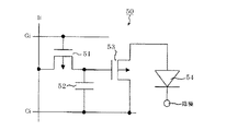
次に、画素の動作について説明する。図5は、図4の表示装置に配置されている1つの画素を構成する回路を示す回路図である。図5の画素回路50においては、ゲート選択線Giに選択信号が印加されると、第一の薄膜トランジスタ(TFT1)51がONになり、コンデンサー(Cadd)52に画像信号Iiが供給され、第二の薄膜トランジスタ(TFT2)53のゲート電圧を決定する。有機発光素子54には第二の薄膜トランジスタ(TFT2)53のゲート電圧に応じて電流供給線Ciより電流が供給される。ここで、第二の薄膜トランジスタ(TFT2)53のゲート電位は、第一の薄膜トランジスタ(TFT1)51が次に走査選択されるまでコンデンサー(Cadd)52に保持される。このため、有機発光素子54には、次の走査が行われるまで電流が流れ続ける。これにより1フレーム期間中常に有機発光素子54を発光させることが可能となる。
Next, the operation of the pixel will be described. FIG. 5 is a circuit diagram showing a circuit constituting one pixel arranged in the display device of FIG. In the
図6は、図4の表示装置で使用されるTFT基板の断面構造の一例を示した模式図である。TFT基板の製造工程の一例を示しながら、構造の詳細を以下に説明する。図6の表示装置60を製造する際には、まずガラス等の基板61上に、上部に作られる部材(TFT又は有機化合物層)を保護するための防湿膜62がコートされる。防湿膜62を構成する材料として、酸化ケイ素又は酸化ケイ素と窒化ケイ素との複合体等が用いられる。次に、スパッタリングによりCr等の金属を製膜することで、所定の回路形状にパターニングしてゲート電極63を形成する。続いて、酸化シリコン等をプラズマCVD法又は触媒化学気相成長法(cat−CVD法)等により製膜し、パターニングしてゲート絶縁膜64を形成する。次に、プラズマCVD法等により(場合によっては290℃以上の温度でアニールして)シリコン膜を製膜し、回路形状に従ってパターニングすることで半導体層65を形成する。
FIG. 6 is a schematic view showing an example of a cross-sectional structure of a TFT substrate used in the display device of FIG. Details of the structure will be described below while showing an example of the manufacturing process of the TFT substrate. When the
さらに、この半導体膜65にドレイン電極66とソース電極67を設けることでTFT素子68を作製し、図5に示すような回路を形成する。次に、このTFT素子68の上部に絶縁膜69を形成する。次に、コンタクトホール(スルーホール)70を、金属からなる有機発光素子用の陽極71とソース電極67が接続するように形成する。
Furthermore, the
この陽極71の上に、多層あるいは単層の有機化合物層72と、陰極73を順次積層することにより、表示装置60を得ることができる。このとき、有機発光素子の劣化を防ぐために第一の保護層74や第二の保護層75を設けてもよい。本発明のフルオレン化合物を使用した表示装置を駆動することにより、良好な画質で、長時間表示にも安定な表示が可能になる。
The
尚、上記の表示装置は、スイッチング素子に特に限定はなく、単結晶シリコン基板やMIM素子、a−Si型等でも容易に応用することができる。 Note that the display device is not particularly limited to a switching element, and can be easily applied to a single crystal silicon substrate, an MIM element, an a-Si type, or the like.
以下に実施例を挙げて本発明を具体的に説明する。ただし、本発明はこれらに限定されるものではない。 The present invention will be specifically described below with reference to examples. However, the present invention is not limited to these.
<実施例1>(例示化合物P112の合成) <Example 1> (Synthesis of Exemplified Compound P112)
窒素雰囲気下、以下に示す試薬、溶媒を200mLナスフラスコに投入した。
ボロン酸エステルP−Bpin4:1.0g(1.32mmol)
4−ブロモ−2,7−ジ−tert−ブチル−9,9−ジメチルフルオレン:2.03g(5.82mmol)
トルエン:60mL
エタノール:30mL
In a nitrogen atmosphere, the following reagents and solvents were put into a 200 mL eggplant flask.
Boronic ester P-Bpin 4 : 1.0 g (1.32 mmol)
4-Bromo-2,7-di-tert-butyl-9,9-dimethylfluorene: 2.03 g (5.82 mmol)
Toluene: 60 mL
Ethanol: 30mL
さらに、10重量%炭酸ナトリウム水溶液30mLを加えた後、反応溶液を室温で30分攪拌した。続いて、テトラキス(トリフェニルホスフィン)パラジウム150mg(0.13mmol)を加えた後、反応溶液を還流させながら3時間撹拌した。反応終了後、反応溶液を水で洗浄し、硫酸マグネシウムにて乾燥させた後に減圧濃縮した。次に、濃縮した反応溶液を、メタノールを用いた再沈殿を行うことで精製することにより、例示化合物P112を0.59g得た(収率30%)。 Further, after adding 30 mL of a 10 wt% aqueous sodium carbonate solution, the reaction solution was stirred at room temperature for 30 minutes. Subsequently, 150 mg (0.13 mmol) of tetrakis (triphenylphosphine) palladium was added, and then the reaction solution was stirred for 3 hours while refluxing. After completion of the reaction, the reaction solution was washed with water, dried over magnesium sulfate, and concentrated under reduced pressure. Next, the concentrated reaction solution was purified by reprecipitation using methanol to obtain 0.59 g of Exemplified Compound P112 (yield 30%).
得られた化合物の同定を行った結果を以下に示す。
[MALDI−TOF−MS(マトリックス支援イオン化−飛行時間型質量分析)]実測値:m/z=1470.39、計算値:C112H124=1468.97
[1H−NMR(400MHz、CDCl3)] δ 8.40(s,4H),7.84(s,4H),7.55−7.27(m,12H),7.23−6.85(m,8H),1.52(s,24H),1.38(s,36H),1.29(s,36H)
The results of identification of the obtained compound are shown below.
[MALDI-TOF-MS (matrix-assisted ionization-time-of-flight mass spectrometry)] Measured value: m / z = 1470.39, calculated value: C 112 H 124 = 1468.97
[ 1 H-NMR (400 MHz, CDCl 3 )] δ 8.40 (s, 4H), 7.84 (s, 4H), 7.55 to 7.27 (m, 12H), 7.23-6. 85 (m, 8H), 1.52 (s, 24H), 1.38 (s, 36H), 1.29 (s, 36H)
<実施例2>(例示化合物P201の合成) <Example 2> (Synthesis of Exemplified Compound P201)
窒素雰囲気下、以下に示す試薬、溶媒を200mLナスフラスコに投入した。
ボロン酸エステルP−Bpin4:1.0g(1.32mmol)
1−ブロモナフタレン:1.20g(5.82mmol)
トルエン:60mL
エタノール:30mL
In a nitrogen atmosphere, the following reagents and solvents were put into a 200 mL eggplant flask.
Boronic ester P-Bpin 4 : 1.0 g (1.32 mmol)
1-bromonaphthalene: 1.20 g (5.82 mmol)
Toluene: 60 mL
Ethanol: 30mL
さらに、10重量%炭酸ナトリウム水溶液30mLを加えた後、反応溶液を室温で30分攪拌した。続いて、テトラキス(トリフェニルホスフィン)パラジウム150mg(0.13mmol)を加えて、反応溶液を還流させながら3時間撹拌した。次に、反応溶液を冷却した後、析出した結晶を濾取することで粗生成物を得た。次に、この粗生成物をトルエン溶媒による再結晶で精製することにより、例示化合物P201を0.94g得た(収率94%)。 Further, after adding 30 mL of a 10 wt% aqueous sodium carbonate solution, the reaction solution was stirred at room temperature for 30 minutes. Subsequently, 150 mg (0.13 mmol) of tetrakis (triphenylphosphine) palladium was added, and the reaction solution was stirred for 3 hours while refluxing. Next, after cooling the reaction solution, the precipitated crystals were collected by filtration to obtain a crude product. Next, this crude product was purified by recrystallization using a toluene solvent, thereby obtaining 0.94 g of Exemplified Compound P201 (yield 94%).
得られた化合物の同定を行った結果を以下に示す。
[MALDI−TOF−MS]実測値:m/z=756.11、計算値:C60H36=756.28
[1H−NMR(400MHz、CDCl3)] δ 8.39(s,4H),8.04(d,4H),7.95−7.85(m,12H),7.65−7.40(m,16H)
The results of identification of the obtained compound are shown below.
[MALDI-TOF-MS] Measured value: m / z = 756.11, calculated value: C 60 H 36 = 756.28
[ 1 H-NMR (400 MHz, CDCl 3 )] δ 8.39 (s, 4H), 8.04 (d, 4H), 7.95-7.85 (m, 12H), 7.65-7. 40 (m, 16H)
<実施例3>
図3に示す有機発光素子を以下に示す方法で作製した。
<Example 3>
The organic light emitting device shown in FIG. 3 was produced by the following method.
まずガラス基板(基板1)上に、スパッタ法により酸化錫インジウム(ITO)を成膜して陽極2を形成した。このとき陽極2の膜厚を120nmとした。このようにITOが成膜されている基板を透明導電性支持基板(ITO基板)として使用した。次に、このITO基板を、10-4Paの真空チャンバー内に移動させた後、抵抗加熱による真空蒸着によって、当該ITO基板上に以下の有機化合物層及び電極層を連続的に成膜した。具体的には、まず陽極2上にα−NPDを成膜し正孔輸送層5を形成した。このとき正孔輸送層5の膜厚を15nmとした。次に、正孔輸送層5上に、ホストである化合物BH−1とゲストである例示化合物P201とを、発光層3全体に対する例示化合物P201の含有量が2重量%となるように共蒸着して発光層3を形成した。このとき発光層3の膜厚を30nmとした。次に、発光層3上に、Bphenを成膜し電子輸送層6を形成した。このとき電子輸送層6の膜厚を20nmとした。次に、電子輸送層6上に、KFを成膜しKF膜を形成した。このときKF膜の膜厚を1nmとした。次に、KF膜上に、Alを成膜しAl膜を形成した。このときAl膜の膜厚を150nmとした。ここで、KF膜及びAl膜は、陰極4として機能する。 First, an indium tin oxide (ITO) film was formed on a glass substrate (substrate 1) by sputtering to form an anode 2. At this time, the film thickness of the anode 2 was 120 nm. Thus, the board | substrate with which ITO was formed into a film was used as a transparent conductive support substrate (ITO board | substrate). Next, after moving this ITO substrate into a vacuum chamber of 10 −4 Pa, the following organic compound layers and electrode layers were continuously formed on the ITO substrate by vacuum deposition by resistance heating. Specifically, first, α-NPD was formed on the anode 2 to form the hole transport layer 5. At this time, the thickness of the hole transport layer 5 was set to 15 nm. Next, the compound BH-1 as a host and the exemplified compound P201 as a guest are co-deposited on the hole transport layer 5 so that the content of the exemplified compound P201 with respect to the entire light emitting layer 3 is 2% by weight. Thus, the light emitting layer 3 was formed. At this time, the thickness of the light emitting layer 3 was set to 30 nm. Next, Bphen was formed on the light emitting layer 3 to form the electron transport layer 6. At this time, the thickness of the electron transport layer 6 was set to 20 nm. Next, a KF film was formed on the electron transport layer 6 to form a KF film. At this time, the thickness of the KF film was 1 nm. Next, an Al film was formed on the KF film to form an Al film. At this time, the thickness of the Al film was set to 150 nm. Here, the KF film and the Al film function as the cathode 4.
次に、有機発光素子が、水分の吸着によって素子劣化が起こらないように、乾燥空気雰囲気中で保護用ガラス板をかぶせ、アクリル樹脂系接着材で封止した。以上のようにして有機発光素子を得た。 Next, the organic light emitting device was covered with a protective glass plate in a dry air atmosphere and sealed with an acrylic resin adhesive so that the device did not deteriorate due to moisture adsorption. An organic light emitting device was obtained as described above.
得られた有機発光素子について、ITO電極(陽極2)を正極、Al電極(陰極4)を負極にして、4.5Vの印加電圧をかけたところ、発光効率が5.7cd/Aで、輝度2000cd/m2の青色発光が観測された。またこの素子において、CIE色度座標は、(x,y)=(0.13,0.26)であった。さらに、この素子を100mA/cm2の定電流密度を保ちながら100時間耐久駆動させると、初期輝度からの輝度減少率は20%であった。 When the applied voltage of 4.5 V was applied to the obtained organic light emitting device with the ITO electrode (anode 2) as the positive electrode and the Al electrode (cathode 4) as the negative electrode, the luminous efficiency was 5.7 cd / A and the luminance A blue emission of 2000 cd / m 2 was observed. In this device, CIE chromaticity coordinates were (x, y) = (0.13, 0.26). Further, when this element was driven for 100 hours while maintaining a constant current density of 100 mA / cm 2 , the luminance reduction rate from the initial luminance was 20%.
<比較例1>
実施例3において、発光層のゲストとして、例示化合物P201の代わりに下記に示すTBPを使用した他は、実施例3と同様の方法で素子を作製した。
<Comparative Example 1>
In Example 3, a device was produced in the same manner as in Example 3 except that TBP shown below was used instead of the exemplified compound P201 as a guest of the light emitting layer.
得られた素子について実施例3と同様の評価を行ったところ、5.1Vの印加電圧において、発光効率が3.9cd/Aで、輝度2000cd/m2の青緑色発光が観測された。またこの素子において、CIE色度座標は、(x,y)=(0.18,0.35)であった。さらに、この素子を100mA/cm2の定電流密度を保ちながら100時間耐久駆動させると、初期輝度からの輝度減少率は48%であった。 When the obtained device was evaluated in the same manner as in Example 3, blue-green light emission with a luminance efficiency of 3.9 cd / A and a luminance of 2000 cd / m 2 was observed at an applied voltage of 5.1 V. In this device, the CIE chromaticity coordinates were (x, y) = (0.18, 0.35). Further, when this element was driven for 100 hours while maintaining a constant current density of 100 mA / cm 2 , the luminance reduction rate from the initial luminance was 48%.
<実施例4>
図3に示す構造の有機発光素子を作製した。
<Example 4>
An organic light emitting device having the structure shown in FIG. 3 was produced.
まず実施例3と同様の方法でITO基板を作製した。次に、このITO基板上に、バイエル社製のPEDOT(有機EL用)を滴下し、回転数1000rpmで30秒間スピンコートすることにより薄膜を作製した。次に、真空チャンバー内において120℃で1時間加熱乾燥することにより、正孔輸送層5を形成した。このとき正孔輸送層5の膜厚を35nmとした。次に、以下に示す試薬、溶媒を混合し塗布液を調製した。
脱水クロロホルム:5.0g
例示化合物P112:5mg
化合物BH1:50mg
First, an ITO substrate was produced in the same manner as in Example 3. Next, PEDOT (for organic EL) made by Bayer was dropped on the ITO substrate, and a thin film was produced by spin coating at a rotational speed of 1000 rpm for 30 seconds. Next, the hole transport layer 5 was formed by heating and drying at 120 ° C. for 1 hour in a vacuum chamber. At this time, the thickness of the hole transport layer 5 was set to 35 nm. Next, the following reagent and solvent were mixed to prepare a coating solution.
Dehydrated chloroform: 5.0 g
Exemplary compound P112: 5 mg
Compound BH1: 50 mg
次に、窒素雰囲気にしたグローブボックス内で、正孔輸送層5上に、先程調製した塗布液を滴下し、回転数2000rpmで20秒間スピンコートした。次に、真空チャンバー内において120℃で1時間加熱乾燥することにより、発光層3を形成した。このとき発光層3の膜厚を45nmとした。 Next, the previously prepared coating solution was dropped onto the hole transport layer 5 in a glove box in a nitrogen atmosphere, and spin coated at a rotational speed of 2000 rpm for 20 seconds. Next, the light emitting layer 3 was formed by heat-drying at 120 degreeC for 1 hour in a vacuum chamber. At this time, the thickness of the light emitting layer 3 was set to 45 nm.
次に、発光層3まで形成されているITO基板を真空蒸着チャンバー内に装着した。次に、発光層3上に、Bphenを真空蒸着して電子輸送層6を形成した。このとき電子輸送層6の膜厚を40nmとした。ここまでの工程において、ITO基板上に形成されている有機化合物層の総膜厚は120nmである。次に、KFを真空蒸着してKF膜を形成した。このときKF膜の膜厚1nmとした。次に、KF膜上に、Alを真空蒸着してAl膜を形成した。このときAl膜の膜厚を120nmとした。ここで、KF膜及びAl膜は、陰極4として機能する。以上のようにして有機発光素子を得た。 Next, the ITO substrate formed up to the light emitting layer 3 was mounted in a vacuum deposition chamber. Next, Bphen was vacuum-deposited on the light emitting layer 3 to form the electron transport layer 6. At this time, the thickness of the electron transport layer 6 was set to 40 nm. In the steps so far, the total film thickness of the organic compound layer formed on the ITO substrate is 120 nm. Next, KF was vacuum deposited to form a KF film. At this time, the thickness of the KF film was 1 nm. Next, Al was vacuum-deposited on the KF film to form an Al film. At this time, the thickness of the Al film was set to 120 nm. Here, the KF film and the Al film function as the cathode 4. An organic light emitting device was obtained as described above.
得られた有機発光素子について、ITO電極(陽極2)を正極、Al電極(陰極4)を負極にして、DC電圧を印加することにより素子の特性を評価した。この素子において、輝度を500cd/m2としたときの電流効率は2.1cd/Aであった。またこのときの発光色は、CIE色度座標で(x,y)=(0.14,0.30)であった。 About the obtained organic light emitting element, the characteristic of the element was evaluated by applying a DC voltage with the ITO electrode (anode 2) as a positive electrode and the Al electrode (cathode 4) as a negative electrode. In this device, the current efficiency was 2.1 cd / A when the luminance was 500 cd / m 2 . The emission color at this time was (x, y) = (0.14, 0.30) in CIE chromaticity coordinates.
<実施例5>
図3に示す有機発光素子を以下に示す方法で作製した。
<Example 5>
The organic light emitting device shown in FIG. 3 was produced by the following method.
実施例3と同様の方法でITO基板を作製した。次に、このITO基板を、10-4Paの真空チャンバー内に移動させた後、抵抗加熱による真空蒸着によって、当該ITO基板上に以下の有機化合物層及び電極層を連続的に成膜した。具体的には、まず陽極2上に、α−NPDを成膜し正孔輸送層5を形成した。このとき正孔輸送層5の膜厚を20nmとした。次に、正孔輸送層5上に、ホストである例示化合物P201とゲストである下記に示されるGD−1とを、発光層3全体に対するGD−1の含有量が3重量%となるように共蒸着して発光層3を形成した。このとき発光層3の膜厚を30nmとした。次に、発光層3上に、Bphenを成膜し電子輸送層6を形成した。このとき電子輸送層6の膜厚を30nmとした。次に、電子輸送層6上にKFを成膜しKF膜を形成した。このときKF膜の膜厚を1nmとした。次に、KF膜上にAlを成膜しAl膜を形成した。このときAl膜の膜厚を120nmとした。ここで、KF膜及びAl膜は、陰極4として機能する。 An ITO substrate was produced in the same manner as in Example 3. Next, after moving this ITO substrate into a vacuum chamber of 10 −4 Pa, the following organic compound layers and electrode layers were continuously formed on the ITO substrate by vacuum deposition by resistance heating. Specifically, first, α-NPD was formed on the anode 2 to form the hole transport layer 5. At this time, the thickness of the hole transport layer 5 was set to 20 nm. Next, on the hole transport layer 5, the exemplified compound P201 as a host and GD-1 shown below as a guest are contained so that the content of GD-1 with respect to the entire light emitting layer 3 is 3% by weight. The light emitting layer 3 was formed by co-evaporation. At this time, the thickness of the light emitting layer 3 was set to 30 nm. Next, Bphen was formed on the light emitting layer 3 to form the electron transport layer 6. At this time, the thickness of the electron transport layer 6 was set to 30 nm. Next, a KF film was formed on the electron transport layer 6 to form a KF film. At this time, the thickness of the KF film was 1 nm. Next, Al was formed on the KF film to form an Al film. At this time, the thickness of the Al film was set to 120 nm. Here, the KF film and the Al film function as the cathode 4.
次に、有機発光素子が、水分の吸着によって素子劣化が起こらないように、乾燥空気雰囲気中で保護用ガラス板をかぶせ、アクリル樹脂系接着材で封止した。以上のようにして有機発光素子を得た。 Next, the organic light emitting device was covered with a protective glass plate in a dry air atmosphere and sealed with an acrylic resin adhesive so that the device did not deteriorate due to moisture adsorption. An organic light emitting device was obtained as described above.
このようにして得られた有機発光素子について、ITO電極(陽極2)を正極、Al電極(陰極4)を負極にして、4.1Vの印加電圧をかけたところ、発光効率が14.8cd/Aで、輝度1800cd/m2の緑色の発光が観測された。またこの素子において、CIE色度座標は、(x,y)=(0.20,0.69)であった。さらに、この素子を100mA/cm2の定電流密度を保ちながら200時間耐久駆動させると、初期輝度からの輝度減少率は26%であった。 With respect to the organic light-emitting device thus obtained, when an applied voltage of 4.1 V was applied with the ITO electrode (anode 2) as the positive electrode and the Al electrode (cathode 4) as the negative electrode, the luminous efficiency was 14.8 cd / In A, green light emission with a luminance of 1800 cd / m 2 was observed. In this device, the CIE chromaticity coordinates were (x, y) = (0.20, 0.69). Furthermore, when this element was driven for 200 hours while maintaining a constant current density of 100 mA / cm 2 , the luminance reduction rate from the initial luminance was 26%.
1 基板
2 陽極
3 発光層
4 陰極
5 正孔輸送層
6 電子輸送層
10,20,30 有機発光素子
40,60 表示装置
41 走査信号ドライバー
42 情報信号ドライバー
43 電流供給源
44,50 画素回路
51 第一の薄膜トランジスタ(TFT)
52 コンデンサー(Cadd)
53 第二の薄膜トランジスタ(TFT)
61 基板
62 防湿層
63 ゲート電極
64 ゲート絶縁膜
65 半導体膜
66 ドレイン電極
67 ソース電極
68 TFT素子
69 絶縁膜
70 コンタクトホール(スルーホール)
71 陽極
72 有機化合物層
73 陰極
74 第一の保護層
75 第二の保護層
DESCRIPTION OF SYMBOLS 1 Substrate 2 Anode 3 Light emitting layer 4 Cathode 5 Hole transport layer 6
52 Capacitor (C add )
53 Second Thin Film Transistor (TFT)
61
71
Claims (11)
式(1)において、Ar1乃至Ar4は、それぞれ下記一般式(2)又は(3)で示される同一の置換基を表す。
式(2)において、Y1及びY2は、それぞれアルキル基を表す。尚、Y1 又はY2 で表されるアルキル基に、アルキル基、芳香族炭化水素基、ジメチルアミノ基、ジエチルアミノ基、ジベンジルアミノ基、ジフェニルアミノ基、ジトリルアミノ基、ジアニソリルアミノ基、アルコキシ基、アリールオキシ基、ハロゲン原子、水酸基、シアノ基又はニトロ基がさらに置換されていてもよい。)
In the formula (1), Ar 1 to Ar 4 each represent the same substituent represented by the following general formula (2) or (3).
In Formula (2), Y 1 and Y 2 each represents an alkyl group . In addition, an alkyl group represented by Y 1 or Y 2 is an alkyl group, an aromatic hydrocarbon group , a dimethylamino group, a diethylamino group, a dibenzylamino group, a diphenylamino group, a ditolylamino group, a dianisolylamino group, an alkoxy group. The group, aryloxy group, halogen atom, hydroxyl group, cyano group or nitro group may be further substituted. )
特徴とする、請求項1に記載のペリレン化合物。
とする、請求項1に記載のペリレン化合物。
前記陽極と前記陰極との間に配置される有機化合物層と、から構成され、
前記陽極及び前記陰極のいずれかが透明又は半透明であり、
前記有機化合物層に請求項1乃至3に記載のペリレン化合物が少なくとも一種類含まれることを特徴とする、有機発光素子。 An anode and a cathode;
An organic compound layer disposed between the anode and the cathode, consists of,
One of the anode and the cathode is transparent or semi-transparent,
An organic light emitting device comprising at least one perylene compound according to claim 1 in the organic compound layer.
前記有機発光素子をアクティブマトリックス方式で駆動することを特徴とする、表示装置。 An organic light emitting device according to any one of claims 4 to 8, comprising:
A display device, wherein the organic light emitting element is driven by an active matrix method.
Priority Applications (4)
| Application Number | Priority Date | Filing Date | Title |
|---|---|---|---|
| JP2008305859A JP5424622B2 (en) | 2008-12-01 | 2008-12-01 | Perylene compound and organic light emitting device using the same |
| PCT/JP2009/070358 WO2010064694A1 (en) | 2008-12-01 | 2009-11-27 | Perylene compound and organic light emitting device using the compound |
| US13/131,853 US9051232B2 (en) | 2008-12-01 | 2009-11-27 | Perylene compound and organic light emitting device using the compound |
| EP09830460.3A EP2370384A4 (en) | 2008-12-01 | 2009-11-27 | Perylene compound and organic light emitting device using the compound |
Applications Claiming Priority (1)
| Application Number | Priority Date | Filing Date | Title |
|---|---|---|---|
| JP2008305859A JP5424622B2 (en) | 2008-12-01 | 2008-12-01 | Perylene compound and organic light emitting device using the same |
Publications (3)
| Publication Number | Publication Date |
|---|---|
| JP2010126511A JP2010126511A (en) | 2010-06-10 |
| JP2010126511A5 JP2010126511A5 (en) | 2012-04-26 |
| JP5424622B2 true JP5424622B2 (en) | 2014-02-26 |
Family
ID=42233341
Family Applications (1)
| Application Number | Title | Priority Date | Filing Date |
|---|---|---|---|
| JP2008305859A Active JP5424622B2 (en) | 2008-12-01 | 2008-12-01 | Perylene compound and organic light emitting device using the same |
Country Status (4)
| Country | Link |
|---|---|
| US (1) | US9051232B2 (en) |
| EP (1) | EP2370384A4 (en) |
| JP (1) | JP5424622B2 (en) |
| WO (1) | WO2010064694A1 (en) |
Families Citing this family (13)
| Publication number | Priority date | Publication date | Assignee | Title |
|---|---|---|---|---|
| GB0814161D0 (en) * | 2008-08-01 | 2008-09-10 | Cambridge Display Tech Ltd | Blue-light emitting material |
| US9024304B2 (en) * | 2011-03-29 | 2015-05-05 | Dae Joo Electronic Materials Co., Ltd. | Naphthalene derivative, organic material including the same, and organic electroluminescent device including the same |
| KR101305869B1 (en) * | 2011-10-12 | 2013-09-09 | 포항공과대학교 산학협력단 | Simplified organic emitting diode and method for preparing the same |
| US10642087B2 (en) | 2014-05-23 | 2020-05-05 | Eyesafe, Llc | Light emission reducing compounds for electronic devices |
| US10901125B2 (en) | 2014-05-23 | 2021-01-26 | Eyesafe, Llc | Light emission reducing compounds for electronic devices |
| JPWO2019220769A1 (en) * | 2018-05-18 | 2020-05-28 | パナソニックIpマネジメント株式会社 | Flow battery |
| US20220048836A1 (en) * | 2018-09-12 | 2022-02-17 | Merck Patent Gmbh | Materials for organic electroluminescent devices |
| US10955697B2 (en) | 2018-11-28 | 2021-03-23 | Eyesafe Inc. | Light emission modification |
| US11126033B2 (en) | 2018-11-28 | 2021-09-21 | Eyesafe Inc. | Backlight unit with emission modification |
| US11592701B2 (en) | 2018-11-28 | 2023-02-28 | Eyesafe Inc. | Backlight unit with emission modification |
| US11810532B2 (en) | 2018-11-28 | 2023-11-07 | Eyesafe Inc. | Systems for monitoring and regulating harmful blue light exposure from digital devices |
| US10971660B2 (en) | 2019-08-09 | 2021-04-06 | Eyesafe Inc. | White LED light source and method of making same |
| CN112824367B (en) * | 2019-11-21 | 2024-04-05 | 乐金显示有限公司 | Organic compound, organic light emitting diode and organic light emitting display device including the same |
Family Cites Families (12)
| Publication number | Priority date | Publication date | Assignee | Title |
|---|---|---|---|---|
| JP3693128B2 (en) | 1996-03-08 | 2005-09-07 | 出光興産株式会社 | Organic electroluminescence device |
| JPH1036832A (en) | 1996-07-30 | 1998-02-10 | Mitsubishi Chem Corp | Organic electroluminescence element |
| JP3578954B2 (en) * | 2000-01-12 | 2004-10-20 | 三星エスディアイ株式会社 | Organic electroluminescence device |
| JP4316841B2 (en) | 2001-07-04 | 2009-08-19 | Tdk株式会社 | Method for synthesizing perylene derivative, perylene derivative, and organic EL device |
| US7282275B2 (en) * | 2002-04-19 | 2007-10-16 | 3M Innovative Properties Company | Materials for organic electronic devices |
| JP4345387B2 (en) | 2003-07-25 | 2009-10-14 | チッソ株式会社 | Perylene derivative and organic electroluminescence device using the same |
| JP2005068366A (en) | 2003-08-27 | 2005-03-17 | Toyo Ink Mfg Co Ltd | Material for organic electroluminescent element and organic electroluminescent element |
| JP2005075868A (en) * | 2003-08-29 | 2005-03-24 | Fujitsu Ltd | Fluorescent material, organic electroluminescent element and organic electroluminescent display |
| JP2005113072A (en) * | 2003-10-10 | 2005-04-28 | Toyo Ink Mfg Co Ltd | Material for organic electroluminescent element and organic electroluminescent element produced by using the same |
| US7175922B2 (en) | 2003-10-22 | 2007-02-13 | Eastman Kodak Company | Aggregate organic light emitting diode devices with improved operational stability |
| US7429822B2 (en) * | 2003-10-28 | 2008-09-30 | Sharp Kabushiki Kaisha | Organic electroluminescence device having a cathode with a metal layer that includes a first metal and a low work function metal |
| KR20090111915A (en) * | 2008-04-23 | 2009-10-28 | (주)그라쎌 | Novel organic electroluminescent compounds and organic electroluminescent device using the same |
-
2008
- 2008-12-01 JP JP2008305859A patent/JP5424622B2/en active Active
-
2009
- 2009-11-27 EP EP09830460.3A patent/EP2370384A4/en not_active Withdrawn
- 2009-11-27 US US13/131,853 patent/US9051232B2/en active Active
- 2009-11-27 WO PCT/JP2009/070358 patent/WO2010064694A1/en active Application Filing
Also Published As
| Publication number | Publication date |
|---|---|
| US9051232B2 (en) | 2015-06-09 |
| EP2370384A4 (en) | 2014-10-29 |
| US20110227057A1 (en) | 2011-09-22 |
| JP2010126511A (en) | 2010-06-10 |
| WO2010064694A1 (en) | 2010-06-10 |
| EP2370384A1 (en) | 2011-10-05 |
Similar Documents
| Publication | Publication Date | Title |
|---|---|---|
| JP5424622B2 (en) | Perylene compound and organic light emitting device using the same | |
| JP5183142B2 (en) | Binaphthyl compound and organic light-emitting device using the same | |
| JP5709382B2 (en) | Novel chrysene compound and organic light emitting device having the same | |
| JP5110901B2 (en) | Material for organic light emitting device and organic light emitting device using the same | |
| JP2008156316A (en) | Material for organic light-emitting element and organic light-emitting element using the same | |
| US20110198582A1 (en) | Organic light-emitting device | |
| JP5523060B2 (en) | Novel biclicene compound and organic light emitting device having the same | |
| JP5574860B2 (en) | Materials for organic light emitting devices having a dibenzosuberon skeleton | |
| JP2010111635A (en) | New azaindenochrysene derivative and organic light-emitting element | |
| JP5408902B2 (en) | Dibenzo [c, g] fluorene compound and organic light emitting device using the same | |
| JP4950460B2 (en) | Organic light emitting device | |
| JP4795463B2 (en) | Novel benzo [c] phenanthrene compound and organic light-emitting device having the same | |
| JP5110922B2 (en) | Asymmetric fluorene compound and organic light emitting device using the same | |
| JP5656493B2 (en) | Novel condensed polycyclic compound and organic light emitting device having the same | |
| CN110981867B (en) | Compound, electronic element and electronic device | |
| JP5534705B2 (en) | Novel condensed polycyclic compounds and organic light emitting devices | |
| JP2011236158A (en) | Condensed polycyclic compound and organic light-emitting element using the same | |
| JP2010132651A (en) | DIBENZO[c,g]FLUORENE COMPOUND, AND ORGANIC LIGHT-EMITTING DEVICE USING THE SAME |
Legal Events
| Date | Code | Title | Description |
|---|---|---|---|
| A621 | Written request for application examination |
Free format text: JAPANESE INTERMEDIATE CODE: A621 Effective date: 20111201 |
|
| A521 | Request for written amendment filed |
Free format text: JAPANESE INTERMEDIATE CODE: A523 Effective date: 20120312 |
|
| A131 | Notification of reasons for refusal |
Free format text: JAPANESE INTERMEDIATE CODE: A131 Effective date: 20130806 |
|
| A521 | Request for written amendment filed |
Free format text: JAPANESE INTERMEDIATE CODE: A523 Effective date: 20131001 |
|
| TRDD | Decision of grant or rejection written | ||
| A01 | Written decision to grant a patent or to grant a registration (utility model) |
Free format text: JAPANESE INTERMEDIATE CODE: A01 Effective date: 20131029 |
|
| A61 | First payment of annual fees (during grant procedure) |
Free format text: JAPANESE INTERMEDIATE CODE: A61 Effective date: 20131126 |
|
| R151 | Written notification of patent or utility model registration |
Ref document number: 5424622 Country of ref document: JP Free format text: JAPANESE INTERMEDIATE CODE: R151 |