JP5412190B2 - Semiconductor integrated circuit device - Google Patents
Semiconductor integrated circuit device Download PDFInfo
- Publication number
- JP5412190B2 JP5412190B2 JP2009153702A JP2009153702A JP5412190B2 JP 5412190 B2 JP5412190 B2 JP 5412190B2 JP 2009153702 A JP2009153702 A JP 2009153702A JP 2009153702 A JP2009153702 A JP 2009153702A JP 5412190 B2 JP5412190 B2 JP 5412190B2
- Authority
- JP
- Japan
- Prior art keywords
- reference voltage
- circuit
- voltage generation
- intermittent operation
- generation circuit
- Prior art date
- Legal status (The legal status is an assumption and is not a legal conclusion. Google has not performed a legal analysis and makes no representation as to the accuracy of the status listed.)
- Expired - Fee Related
Links
Images


Classifications
-
- G—PHYSICS
- G11—INFORMATION STORAGE
- G11C—STATIC STORES
- G11C5/00—Details of stores covered by group G11C11/00
- G11C5/14—Power supply arrangements, e.g. power down, chip selection or deselection, layout of wirings or power grids, or multiple supply levels
- G11C5/147—Voltage reference generators, voltage or current regulators; Internally lowered supply levels; Compensation for voltage drops
Description
本発明は、半導体集積回路装置の低消費電力化技術に関し、特に、半導体集積回路装置がスタンバイモードに遷移した際のレファレンス回路における消費電力の低減に有効な技術に関する。 The present invention relates to a technology for reducing power consumption of a semiconductor integrated circuit device, and more particularly to a technology effective for reducing power consumption in a reference circuit when the semiconductor integrated circuit device is shifted to a standby mode.
近年、携帯機器や非接触用途のマイコン、SOC製品などにおいて、電池寿命を延ばすことや、RF(Radio Frequency)より微弱なDC電圧/電流を取り出して動作しなければならないなどの理由で、チップの通常動作モード、およびスタンバイ(待機)モードにおける低消費電力化の要求が高まっており、チップ内部電源電圧レベルの可変制御、基板バイアス制御、電源遮断技術などを利用したチップレベルの低リーク化技術が発展する一方で、従来から通常動作モード、およびスタンバイ(待機)モードにおいて、チップ内部で定常的に動作する回路自身の低消費電流化は必然的に行われてきた。 In recent years, in portable devices, non-contact-use microcomputers, SOC products, etc., it is necessary to extend the battery life or to operate by extracting a DC voltage / current weaker than RF (Radio Frequency). There is an increasing demand for low power consumption in normal operation mode and standby mode, and chip level low leakage technology using variable control of chip internal power supply voltage level, substrate bias control, power shutdown technology, etc. On the other hand, conventionally, in the normal operation mode and the standby (standby) mode, the current consumption of the circuit itself that steadily operates in the chip has been inevitably reduced.
一般のチップ性能、ならびに価格帯におけるローエンドからミドルクラスのマイコン製品などでは、CPU(Central Processing Unit)などの動作する内部電源電圧(Vint)とI/O(Input/Output)用の外部電源電圧(Vext)の電圧が異なることが多く、実装コスト削減を目的とした外部電源電圧(Vext)の単一電源化のため内部電源電圧(Vint)生成レギュレータを搭載すること、フラッシュメモリに例示される不揮発性メモリの読み出し、書き込み電圧生成用の正・負高電圧生成用チャージポンプ回路のレファレンス電圧生成回路が必要なこと、スタンバイモードにおいて、RAM(Random Access Memory)の状態保持のため、RAM供給電圧(Vint#RAM)を保持するためチップ内部にRAM保持専用レギュレータを持たせるなどの理由から、チップに電源回路を搭載することが多い。 In general chip performance and low-end to middle-class microcomputer products in the price range, internal power supply voltage (Vint) for operating CPU (Central Processing Unit) and external power supply voltage for I / O (Input / Output) ( Vext) voltage is often different, the internal power supply voltage (Vint) generation regulator is mounted to make the external power supply voltage (Vext) a single power supply for the purpose of reducing mounting costs, and non-volatile as exemplified in flash memory The reference voltage generation circuit of the positive / negative high voltage generation charge pump circuit for generating the read / write voltage generation of the nonvolatile memory is necessary, and in order to maintain the RAM (Random Access Memory) state in the standby mode, the RAM supply voltage ( Vint # RAM) is equipped with a power supply circuit on the chip for reasons such as having a dedicated RAM retention regulator inside the chip. Rukoto often.
この電源回路が上述した通常動作モード、およびスタンバイモードにおいて常に動作する回路に相当するため、低消費電流化を満足できるかどうかがマイコン製品の重要スペックの一つとして考えられている。 Since this power supply circuit corresponds to a circuit that always operates in the normal operation mode and the standby mode described above, it is considered as one of the important specifications of a microcomputer product whether or not low current consumption can be satisfied.
一般に、電源回路内のレファレンス電圧などを生成するアナログ回路(レファレンス電圧生成回路)の消費電流が電源回路の消費電流と面積の大半を占めることが多いが、このレファレンス電圧生成回路の自己消費電流は、回路内に用いた抵抗素子の抵抗値によって決まることが多い。したがって、この抵抗値を大きくしていくことが低消費電流化としては容易である。 In general, the consumption current of an analog circuit (reference voltage generation circuit) that generates a reference voltage in a power supply circuit, etc. often occupies most of the current consumption and area of the power supply circuit. The self-consumption current of this reference voltage generation circuit is Often, this is determined by the resistance value of the resistance element used in the circuit. Therefore, it is easy to reduce the current consumption by increasing the resistance value.
また、抵抗を用いないレファレンス電圧の生成技術としては、たとえば、MOS(Metal Oxide Semiconductor)トランジスタのしきい値差、MOSトランジスタのサブスレッショルドスロープを利用したレファレンス電圧生成回路を用いて抵抗による面積増大を回避し低消費電流化する方法が知られている。 In addition, as a reference voltage generation technique that does not use a resistor, for example, a threshold voltage difference of a MOS (Metal Oxide Semiconductor) transistor, a reference voltage generation circuit that uses a subthreshold slope of a MOS transistor is used to increase the area due to resistance. A method for avoiding this and reducing the current consumption is known.
また、この種の電源回路の低消費電力化技術においては、たとえば、基準電圧発生回路を構成するオペアンプにオシレータを接続し、オシレータの出力電圧に応じてオペアンプを完結的に動作させるものが知られている(たとえば、特許文献1参照)。 Further, in this type of power consumption reduction technology for a power supply circuit, for example, an oscillator is connected to an operational amplifier constituting a reference voltage generation circuit, and the operational amplifier is operated completely according to the output voltage of the oscillator. (For example, refer to Patent Document 1).
ところが、上記のようなレファレンス電圧生成回路の低消費電力化技術では、次のような問題点があることが本発明者により見い出された。 However, the present inventors have found that the above-described technology for reducing the power consumption of the reference voltage generation circuit has the following problems.
すなわち、レファレンス電圧生成回路における抵抗素子の抵抗値を大きくして消費電流を低減する技術では、抵抗値を大きくすることにより、抵抗素子の面積が増大してしまい、特にローエンドのマイコン製品ではチップサイズの増大がチップコスト増大につながり、低消費電流化とチップコストの両立がうまく図れないという問題がある。 That is, in the technology that increases the resistance value of the resistance element in the reference voltage generation circuit to reduce the current consumption, the area of the resistance element increases by increasing the resistance value. This increases the chip cost, and there is a problem that it is difficult to achieve both low current consumption and chip cost.
また、MOSトランジスタのしきい値差、あるいはMOSトランジスタのサブスレッショルドスロープを利用したレファレンス電圧生成回路の場合、これらの回路は出力するレファレンス電圧精度を犠牲にしていることが多い。 In the case of a reference voltage generation circuit using a threshold difference of MOS transistors or a subthreshold slope of MOS transistors, these circuits often sacrifice the accuracy of the output reference voltage.
一方、チップの通常動作モードにおいては、レファレンス電圧精度が高くないと、不揮発性メモリの読み出し、書き込みがうまくいかないなど、チップ内部回路の安定動作、素子信頼性の点から、低精度のレファレンス電圧生成回路をスタンバイモード時専用として用い、通常動作モード時には、別の高精度のレファレンス電圧生成回路を用意して、通常動作モード時とスタンバイモード時でレファレンス電圧生成回路を切り替える手法もあるが、この場合、通常動作モード時とスタンバイモード時のレファレンス電圧生成回路方式の違いからレファレンス電圧レベルが異なることが多いため、切り替え時にレファレンス電圧のレベル変動が問題となってしまう。 On the other hand, in the normal operation mode of the chip, if the reference voltage accuracy is not high, reading and writing of the nonvolatile memory will not be successful. Is used exclusively in the standby mode, and in the normal operation mode, another high-precision reference voltage generation circuit is prepared, and there is a method of switching the reference voltage generation circuit between the normal operation mode and the standby mode. Since the reference voltage level is often different due to the difference in the reference voltage generation circuit method in the normal operation mode and the standby mode, the level fluctuation of the reference voltage becomes a problem at the time of switching.
本発明の目的は、面積の大幅な増大なくレファレンス電圧生成回路を低消費電流化するとともに通常動作モード時とスタンバイモード時においてレファレンス電圧精度の大幅な劣化を抑制することのできる技術を提供することにある。 An object of the present invention is to provide a technique capable of reducing the current consumption of a reference voltage generation circuit without significantly increasing the area and suppressing a significant deterioration in reference voltage accuracy in a normal operation mode and a standby mode. It is in.
本発明の前記ならびにそのほかの目的と新規な特徴については、本明細書の記述および添付図面から明らかになるであろう。 The above and other objects and novel features of the present invention will be apparent from the description of this specification and the accompanying drawings.
本願において開示される発明のうち、代表的なものの概要を簡単に説明すれば、次のとおりである。 Of the inventions disclosed in the present application, the outline of typical ones will be briefly described as follows.
本発明は、レファレンス電圧を生成するレファレンス電圧生成手段を備えた半導体集積回路装置であって、レファレンス電圧生成手段は、該レファレンス電圧を生成するレファレンス電圧生成部と低消費電力モードの1つであるスタンバイモード時に、レファレンス電圧生成部を間欠動作させて前記レファレンス電圧を生成する間欠動作制御部とを備えたものである。 The present invention is a semiconductor integrated circuit device provided with a reference voltage generating means for generating a reference voltage, and the reference voltage generating means is one of a reference voltage generating section for generating the reference voltage and a low power consumption mode. And an intermittent operation control unit that intermittently operates the reference voltage generation unit in the standby mode to generate the reference voltage.
また、本発明は、間欠動作制御部が、基準クロック信号を任意の分周信号に変換し、第1の制御信号、および第2の制御信号を生成する制御信号生成部と、スタンバイモード時に、前記第1の制御信号に基づいて動作し、前記レファレンス電圧生成部が生成したレファレンス電圧を安定化させる充電用レギュレータと、前記充電用レギュレータが安定化させた電源電圧を、前記第2の制御信号に基づいて、サンプル/ホールドするサンプル/ホールド回路と、前記サンプル/ホールド回路の電源電圧をバッファして前記レファレンス電圧として出力するバッファ部と、スタンバイモード時に、前記レファレンス電圧生成部と前記レファレンス電圧生成手段の出力部とを非導通状態とし、前記バッファ部と前記出力部とを導通状態として前記バッファ部から出力される電源電圧をレファレンス電圧として出力するスイッチ部とを備え、前記レファレンス電圧生成部は、制御信号生成部が生成する第1の制御信号に基づいて間欠動作するものである。 Further, according to the present invention, the intermittent operation control unit converts the reference clock signal into an arbitrary divided signal to generate the first control signal and the second control signal, and in the standby mode, A charging regulator that operates based on the first control signal and stabilizes the reference voltage generated by the reference voltage generator, and a power supply voltage that is stabilized by the charging regulator is supplied to the second control signal. A sample / hold circuit for sampling / holding, a buffer unit for buffering the power supply voltage of the sample / hold circuit and outputting it as the reference voltage, and the reference voltage generation unit and the reference voltage generation in the standby mode. The output unit of the means is set in a non-conductive state, and the buffer unit and the output unit are set in a conductive state. And a switch section for outputting a power supply voltage outputted from the file unit as the reference voltage, the reference voltage generator is adapted to intermittent operation based on a first control signal generated by the control signal generating unit.
さらに、本発明は、前記間欠動作制御部が、制御信号生成部に供給する基準クロック信号を生成する発振回路を備えたものである。 Furthermore, in the present invention, the intermittent operation control unit includes an oscillation circuit that generates a reference clock signal to be supplied to the control signal generation unit.
また、本発明は、前記間欠動作制御部が、外部供給される外部電源電圧を降圧した発振用電源電圧を生成し、前記発振回路に電源電圧として供給する発振回路用レギュレータを備えたものである。 In the present invention, the intermittent operation control unit includes an oscillation circuit regulator that generates an oscillation power supply voltage obtained by stepping down an externally supplied external power supply voltage and supplies the oscillation power supply voltage to the oscillation circuit as a power supply voltage. .
さらに、本発明は、前記間欠動作制御部が、スタンバイモードから通常動作モードに遷移した際に、前記レファレンス電圧生成部から出力されるレファレンス電圧上昇を検知して任意の遅延時間が経過した後にスイッチ制御信号を出力し、前記レファレンス電圧生成部と前記レファレンス電圧生成手段の出力部とが導通状態となり、前記バッファ部と前記出力部とが非導通状態となるように前記スイッチ部を切り換える接続切り換え制御部を備えたものである。 Further, according to the present invention, when the intermittent operation control unit detects a rise in the reference voltage output from the reference voltage generation unit when a transition from the standby mode to the normal operation mode and an arbitrary delay time elapses, the switch Connection switching control that outputs a control signal and switches the switch unit so that the reference voltage generation unit and the output unit of the reference voltage generation unit are in a conductive state and the buffer unit and the output unit are in a non-conductive state. It has a part.
また、本発明は、前記レファレンス電圧生成部が、トリミング信号により、生成するレファレンス電圧を調整することのできる機能を有し、前記スタンバイモードに移行した際に、前記トリミング信号による調整を行うリセット期間中に間欠動作しないものである。 Further, the present invention provides a reset period in which the reference voltage generation unit has a function of adjusting a reference voltage to be generated by a trimming signal, and performs the adjustment by the trimming signal when shifting to the standby mode. It does not operate intermittently.
さらに、本願のその他の発明の概要を簡単に示す。 Furthermore, the outline | summary of the other invention of this application is shown briefly.
本発明は、前記レファレンス電圧生成手段の周囲が取り囲まれるようにガードリングが形成されているものである。 In the present invention, a guard ring is formed so as to surround the reference voltage generating means.
また、本発明は、前記レファレンス電圧生成手段が形成された上方を覆うようにメッシュ状のメタルシールド配線が形成されているものである。 In the present invention, a mesh-like metal shield wiring is formed so as to cover the upper part where the reference voltage generating means is formed.
本願において開示される発明のうち、代表的なものによって得られる効果を簡単に説明すれば以下のとおりである。 Among the inventions disclosed in the present application, effects obtained by typical ones will be briefly described as follows.
(1)半導体集積回路装置がスタンバイモードとなった際に、消費電流の大きいレファレンス電圧生成部を間欠的に動作させることで、消費電流を大幅に低減させることができる。 (1) When the semiconductor integrated circuit device is in the standby mode, the current consumption can be significantly reduced by intermittently operating the reference voltage generator having a large current consumption.
(2)また、レファレンス電圧生成手段から発生されるノイズなどを低減させることが可能となり、半導体集積回路装置の信頼性を向上させることができる。 (2) In addition, noise generated from the reference voltage generating means can be reduced, and the reliability of the semiconductor integrated circuit device can be improved.
以下、本発明の実施の形態を図面に基づいて詳細に説明する。なお、実施の形態を説明するための全図において、同一の部材には原則として同一の符号を付し、その繰り返しの説明は省略する。 Hereinafter, embodiments of the present invention will be described in detail with reference to the drawings. Note that components having the same function are denoted by the same reference symbols throughout the drawings for describing the embodiment, and the repetitive description thereof will be omitted.
(実施の形態1)
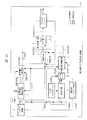
図1は、本発明の実施の形態1による間欠動作基準電圧発生回路の一例を示すブロック図、図2は、図1の間欠動作基準電圧発生回路における動作例を示すタイミングチャート、図3は、図1の間欠動作基準電圧発生回路による低消費電力効果の一例を示す説明図、図4は、図1の間欠動作基準電圧発生回路における外部電源投入時の動作波形と電圧精度との関係を示す説明図、図5は、図1の間欠動作基準電圧発生回路における外部電源投入時の動作波形と電圧精度との他の関係を示す説明図、図6は、図1の間欠動作基準電圧発生回路におけるスタンバイモードから通常動作モードへの遷移時における電圧ドロップの一例を示す説明図、図7は、図1の間欠動作基準電圧発生回路における状態遷移図、図8は、図1の間欠動作基準電圧発生回路を用いて構成した半導体チップにおけるレイアウトの一例を示す説明図、図9は、図8の半導体チップに搭載された間欠動作基準電圧発生回路におけるレイアウトの一例を示す説明図、図10は、図9の間欠動作基準電圧発生回路の上層に形成されたメタルシールド配線の一例を示す説明図、図11は、図9のA−B断面図、図12は、図9の間欠動作基準電圧発生回路の上層に形成されたメタルシールド配線の他の例を示す説明図、図13は、図12のA−B断面図、図14は、図1の間欠動作基準電圧発生回路を用いて構成した半導体チップに搭載された間欠動作基準電圧発生回路におけるガードリングの形成例を示すレイアウト図、図15は、図14のA−B断面図、図16は、本発明の実施の形態1による間欠動作基準電圧発生回路の他の例を示すブロック図、図17は、図16の間欠動作基準電圧発生回路による低消費電力効果の一例を示す説明図である。
(Embodiment 1)
FIG. 1 is a block diagram showing an example of an intermittent operation reference voltage generation circuit according to
本実施の形態1において、間欠動作基準電圧発生回路(IMVREF)1は、たとえば、SOCなどの半導体集積回路装置に設けられている。 In the first embodiment, the intermittent operation reference voltage generation circuit (IMVREF) 1 is provided in a semiconductor integrated circuit device such as an SOC.
この間欠動作基準電圧発生回路1は、図1に示すように、バイアス回路2、基準電圧発生回路3、基準電圧生成回路4、発振回路5、サンプル/ホールド回路である保持容量回路6、バッファ部となるアナログバッファ7、低精度レファレンス回路8、発振回路用レギュレータであるVOSCレギュレータ9、レベルシフタ10、充電用レギュレータである容量充電レギュレータ11、制御信号生成部、および接続切り換え制御部を構成する接続判定コンパレータ12、制御信号生成部、および接続切り換え制御部を構成する接続用ディレイ13、分周制御回路14、およびスイッチ部を構成するスイッチSW1,SW2から構成されている。
As shown in FIG. 1, the intermittent operation reference
また、基準電圧発生回路3、ならびに基準電圧生成回路4によって、レファレンス電圧生成部が構成されており、発振回路5、保持容量回路6、アナログバッファ7、VOSCレギュレータ9、容量充電レギュレータ11、接続判定コンパレータ12、接続用ディレイ13、分周制御回路14、ならびにスイッチSW1,SW2により、間欠動作制御部が構成されている。
The reference
間欠動作基準電圧発生回路1は、これらの回路のうち、消費電流の大きい基準電圧発生回路3、基準電圧生成回路4、ならびに容量充電レギュレータ11を比較的長い周期で間欠的にON/OFFさせることで、平均自己消費電流を下げ、回路全体として低消費電流化を図ったものである(図2)。
Among these circuits, the intermittent operation reference
なお、図1における太線で示すブロックは、半導体集積回路装置の通常動作モード時、およびスタンバイ動作モード時のいずれのモードであっても常時動作を行うブロックを示しており、図1の細線で示すブロックは、半導体集積回路装置がスタンバイ動作モードに遷移すると常時動作ではなく、間欠動作を行うブロックを示している。 The block indicated by the thick line in FIG. 1 indicates a block that always operates in both the normal operation mode and the standby operation mode of the semiconductor integrated circuit device, and is indicated by the thin line in FIG. The block indicates a block that performs intermittent operation instead of continuous operation when the semiconductor integrated circuit device transitions to the standby operation mode.
バイアス回路2は、間欠動作基準電圧発生回路1内のオペアンプなどで用いられる定電流を決める回路であるとともに電圧精度は低いが、発振回路5の動作電圧や基準電圧発生回路3、または基準電圧生成回路4の出力電圧レベルを判定するレファレンス電圧などを生成する。
The
なお、図1において、’NBIAS’が定電流のアナログレファレンス信号であり、’CVREF’が低精度のアナログレファレンス電圧信号である。 In FIG. 1, 'NBIAS' is a constant current analog reference signal, and 'CVREF' is a low-precision analog reference voltage signal.
基準電圧発生回路3は、バイポーラトランジスタの電流密度差から生じるベース−エミッタ間電圧Vbeの差(△Vbe)から取り出した正の温度依存性を持つ電圧(または電流)とバイポーラトランジスタ自身が持つベース−エミッタ間電圧Vbeの負の温度依存性を持つ電圧(または電流)を加算[Vbgr=Vbe+α×△VbeまたはVbgr=
Ibgr×R=(Ibe+α×△Ibe)×R:α、Rは任意]により得られる温度依存性の小さいレファレンス電圧PREVBGRを生成する。
The reference
Ibgr × R = (Ibe + α × ΔIbe) × R: α, R is arbitrary], and a reference voltage PREVBGR having a small temperature dependency is generated.
基準電圧生成回路4は、レファレンス電圧PREVBGRをレベル変換し、チップ内の所望のレファレンス電圧、たとえば、CPUの動作電圧である内部電源電圧VintやRAM保持電圧Vint_RAM用レギュレータのようなスタンバイモード時にレファレンス電圧を保持しておきたいレファレンス電圧PREVREFやPLL/ROMなどに供給するレファレンス電圧(レファレンス電圧VREF PLL,VREF ROM)のようなスタンバイモード時に必ずしも保持する必要のないレファレンス電圧VREF2を生成するものである。
The reference
なお、iビットのトリミング信号TRIMによりレファレンス電圧PREVREF,VREF2をリセット、および通常動作モードにおいて調整できる。 The reference voltages PREVREF and VREF2 can be reset and adjusted in the normal operation mode by the i-bit trimming signal TRIM.
発振回路5は、間欠動作を行うための周波数の遅い基準クロックCLKを生成する。なお、この基準クロックCLKの周波数変動は、一般に、発振回路5にアナログレファレンス信号NBIASにより供給される定電流の精度よりも発振回路5自身の動作電圧VOSC変動に対する感度が高い。
The
したがって、動作電圧VOSCとして外部電源電圧となる外部電源電圧Vextを利用すると周波数変動が大きく安定した間欠動作が得られないため、バイアス回路2で生成したアナログレファレンス電圧信号CVREFを低精度レファレンス回路8により約2倍の電圧レベルに変換したレファレンス電圧CVREF2(=CVREF×2)から、VOSCレギュレータ9を通じて動作電圧VOSCを生成することで周波数変動を低減することが必要である。
Therefore, if the external power supply voltage Vext, which is the external power supply voltage, is used as the operating voltage VOSC, the frequency fluctuation is large and a stable intermittent operation cannot be obtained. Therefore, the analog reference voltage signal CVREF generated by the
周波数変動を低減した基準クロックCLKをレベルシフタ10により、外部電源電圧Vext振幅に変換したクロックCLKUPから分周制御回路14により間欠動作時に基準電圧発生回路3、基準電圧生成回路4、および容量充電レギュレータ11のON/OFFを決めるイネーブル信号VREFONと基準電圧発生回路3、基準電圧生成回路4、ならびに容量充電レギュレータ11がONしている期間に、保持容量回路6内の保持容量CHに充電し(サンプリング)、OFF期間にこの保持容量CHに対してリーク電流パス以外は存在しないように制御する第2の制御信号となるサンプリング/ホールド信号CHOLDSWを生成する(ホールド)。
The reference
また、分周制御回路14は、nビットの分周比切り替え信号FDSELを有し、ON/OFF期間を2n通り設定可能としており、通常/スタンバイ状態選択信号ACTが通常動作モードとすることを示すと、Hiレベルのイネーブル信号VREFONを出力する。
Further, the frequency
アナログバッファ7は、保持容量CHよりスタンバイモード時や、スタンバイモードから通常動作モードに遷移した時にレファレンス電圧を取り出すものであるが、保持容量CHに対して、スイッチSWH以外にリーク電流パスを低減するため、MOSトランジスタのゲート入力で受けるために必要な回路である。
The
接続判定コンパレータ12、および接続用ディレイ13は、スタンバインモードから通常動作モードに遷移した時に、アナログバッファ7の出力とレファレンス電圧PREVREFとを外部入力される通常/スタンバイ状態選択信号ACTの切り替えにより単純に接続してしまうと、図6に示すインピーダンスの違いにより出力電圧ドロップが生じることを回避するため、レファレンス電圧PREVREFの上昇を検知した後、一定の遅延時間後にアナログバッファ7の出力とレファレンス電圧PREVREFとをスイッチSW1,SW2を制御して切り替えるためのものである。
The
図2は、間欠動作基準電圧発生回路1の主な動作波形の一例を示したタイミングチャートである。なお、間欠動作基準電圧発生回路1全体は、外部電源電圧Vextで動作するため、’H’は外部電源電圧Vext、’L’は基準電位Vssである。
FIG. 2 is a timing chart showing an example of main operation waveforms of the intermittent operation reference
図2において、上方から下方にかけては、通常/スタンバイ状態選択信号ACT、第1の制御信号となるイネーブル信号VREFON、サンプリング/ホールド信号CHOLDSW、基準電圧発生回路3または基準電圧生成回路4における出力電圧の上昇や下降を検知した際に接続判定コンパレータ12から出力される出力電圧上昇/下降検知信号CNTOK、スタンバイモードから通常動作モードに遷移した際に接続用ディレイ13から出力されるレファレンス切り替え信号CNTSW、レファレンス電圧PREVBGR、レファレンス電圧PREVREF、保持容量回路6のレファレンス保持容量電圧POSTCHOLD、間欠動作基準電圧発生回路1から出力されるレファレンス電圧VREF、および間欠動作基準電圧発生回路1の自己消費電流IEXTにおける波形をそれぞれ示している。
In FIG. 2, from the upper side to the lower side, the normal / standby state selection signal ACT, the enable signal VREFON serving as the first control signal, the sampling / hold signal HOLDSW, the output voltage of the reference
まず、通常動作モード時は、基準電圧発生回路3、ならびに基準電圧生成回路4が生成するレファレンス電圧PREVREFが定常的に間欠動作基準電圧発生回路1の出力として生成されるため、電圧変動のない安定したレファレンス電位が得られる。
First, in the normal operation mode, the reference voltage PREVREF generated by the reference
一方、スタンバイモード時においては、基準電圧発生回路3、および基準電圧生成回路4がONした期間は通常動作モードとレファレンス電圧レベルが変わらないが、OFF期間はMOSトランジスタのリーク電流(接合リーク、サブスレッショルドリーク、ゲートリークなど)で主にスイッチSWH、および保持容量CHから電荷が抜け電圧レベル低下が起こる。
On the other hand, in the standby mode, the reference voltage level does not change from the normal operation mode during the period when the reference
したがって、スタンバイモード期間中、レファレンス電圧VREFは、電圧リップルを持った波形となる。このレベル低下を低減するためには、基準電圧発生回路3、および基準電圧生成回路4のOFF期間を短くすることが有効だが、低消費電流化の効果が薄れるため、チップの使用環境、プロセス、ならびに製品スペックに合った最適値を見つける必要がある。
Therefore, during the standby mode period, the reference voltage VREF has a waveform with voltage ripple. In order to reduce this level drop, it is effective to shorten the OFF period of the reference
また、図2において、スタンバイモードから通常動作モードに遷移した時にそれらの状態が重なるオーバラップ期間があり、遷移時の電圧ドロップ低減に寄与している。なお、スタンバイモードにおいて、サンプリング/ホールド信号CHOLDSWのH期間が、イネーブル信号VREFONのH期間の後半部分に設定されている理由は、イネーブル信号VREFONがHとなった瞬間に、基準電圧発生回路3、基準電圧生成回路4、および容量充電レギュレータ11がONするが、回路が安定した出力電圧を供給する本来のバイアス状態に達する過渡状態において、一般的に出力電圧のオーバシュートやリンギングが見られることが多いため、電圧が安定した状態で、保持容量CHに電圧を取り込めるようにするためである。
In FIG. 2, there is an overlap period in which these states overlap when transitioning from the standby mode to the normal operation mode, which contributes to voltage drop reduction during transition. In the standby mode, the reason why the H period of the sampling / hold signal HOLDSW is set to the latter half of the H period of the enable signal VREFON is that the reference
図3は、間欠動作基準電圧発生回路1における低消費電流効果の一例を示す説明図である。
FIG. 3 is an explanatory diagram showing an example of the low current consumption effect in the intermittent operation reference
ある外部電源電圧Vext(=3.3V程度)、およびある温度(約27℃)において、通常動作モードでは、間欠動作基準電圧発生回路1内の全てのモジュールがONすることで、消費電流の総和は1362nA程度となっているが、スタンバイモード時に、たとえば、分周比切り替え信号FDSELによって1/8分周を選択すると、消費電流は382nA程度となり、約72%も消費電流を低減することが可能である。
At a certain external power supply voltage Vext (= about 3.3 V) and a certain temperature (about 27 ° C.), in the normal operation mode, all the modules in the intermittent operation reference
図4は、間欠動作基準電圧発生回路1が設けられた半導体集積回路装置への外部電源電圧Vext投入時の動作波形と基準電圧生成回路4にて行うトリミング前後の電圧精度の関係の一例を示す説明図である。
FIG. 4 shows an example of the relationship between the operation waveform when the external power supply voltage Vext is applied to the semiconductor integrated circuit device provided with the intermittent operation reference
電源投入開始よりチップはリセット状態に入り、内部電源電圧VintとCPUの動作周波数の安定を待つことになる。 The chip enters a reset state from the start of power-on, and waits for stabilization of the internal power supply voltage Vint and the CPU operating frequency.
間欠動作基準電圧発生回路1としては、このリセット期間中に不揮発メモリから製品出荷前にチップ毎にテストした結果最適な内部電源電圧Vintになる様に設定した情報を元にトリミングを行う。
The intermittent operation reference
図4では、基準電圧発生回路3、および基準電圧生成回路4を構成するCMOS、抵抗、寄生バイポーラトランジスタなど素子の絶対精度、ならびに相対精度ばらつきにより決まるトリミング前精度(たとえば、±5%以内)がトリミング後精度(たとえば、±1%以内)となっている。
In FIG. 4, the pre-trimming accuracy (for example, within ± 5%) determined by the absolute accuracy of the reference
したがって、通常動作モードでは、トリミング後精度(たとえば、±1%以内)のレファレンス電圧VREF,VREF2が得られる。一方、スタンバイモード時では、基準電圧発生回路3、および基準電圧生成回路4がONする期間において、トリミング後精度(たとえば、±1%以内)で変わらないが、OFF期間においては、リーク電流による電圧レベル低下が影響するため、スタンバイモード時の実精度は、トリミング後精度(たとえば、±1%以内)より劣化する。
Therefore, in the normal operation mode, the reference voltages VREF and VREF2 having an accuracy after trimming (for example, within ± 1%) can be obtained. On the other hand, in the standby mode, the trimming accuracy (for example, within ± 1%) does not change during the period when the reference
このリーク電流による劣化は、チップの使用環境、プロセスなどに左右されるため、製品の消費電流スペックとスタンバイモード時のRAMのメモリ保持電圧の下限値などを参考に、基準電圧発生回路3、および基準電圧生成回路4のON/OFF期間で調整される。図4では、一例として、±1〜5%程度に決められている。
Since the deterioration due to the leakage current depends on the usage environment and process of the chip, the reference
なお、チップのリセット期間中に、間欠動作基準電圧発生回路1は、通常動作モードのように、基準電圧発生回路3と基準電圧生成回路4とを常時ONすべきか、スタンバイモード時のように間欠的にON/OFF動作すべきかについて、図5に示すように間欠的にON/OFF動作すると、低消費電流化のためにOFF期間を長く取る動作のため、起動時間が遅延してしまい、長いリセット期間が必要となるだけでなく、先に述べたリーク電流による電圧レベル低下により、レファレンス電圧PREVBGR、レファレンス電圧PREVREFが十分安定した状態でトリミングを行えないため、トリミング後精度の向上が不十分(たとえば、±5%以内)となる。
During the reset period of the chip, the intermittent operation reference
したがって、リセット期間中は、基準電圧発生回路3、および基準電圧生成回路4を常時ONしておくことが必要である。なお、リセット期間中に間欠動作するOFF期間を短く(たとえば、分周比1/2程度)することで、このリーク電流による劣化を低減しトリミング後精度を向上させることも可能だが、電圧リップルの影響を完全に無視できないため常時ONさせている場合程の電圧精度は得られない。
Therefore, it is necessary to keep the reference
図7は、間欠動作基準電圧発生回路1における状態遷移の一例を示す説明図である。
FIG. 7 is an explanatory diagram illustrating an example of state transition in the intermittent operation reference
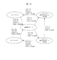
前述したチップのリセット期間中においては、間欠動作基準電圧発生回路1の状態として通常状態J1に当たり、他にスタンバイ状態J2とスタンバイモードから通常状態に遷移するオーバラップ状態J3が存在する。
During the reset period of the chip described above, the intermittent operation reference
図8は、間欠動作基準電圧発生回路1が設けられた半導体集積回路装置における半導体チップCHPのレイアウトの一例を示す説明図である。
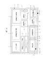
FIG. 8 is an explanatory diagram showing an example of the layout of the semiconductor chip CHP in the semiconductor integrated circuit device provided with the intermittent operation reference
正方形状の半導体チップCHPにおけるそれぞれの外周辺部には、I/O領域15がレイアウトされている。I/O領域15より内側の右上方には、間欠動作基準電圧発生回路1がレイアウトされている。
An I /
間欠動作基準電圧発生回路1の左側には、レギュレータ17がレイアウトされており、その下方には、PLL18がレイアウトされている。このPLL18の下方には、レギュレータ19がレイアウトされており、該レギュレータ19の右側には、レギュレータ20がレイアウトされている。
A
また、これら間欠動作基準電圧発生回路1、ならびにレギュレータ17,19,20によってシステム電源回路16が構成されている。
The intermittent operation reference
レギュレータ19の下方には、RAM21がレイアウトされており、該RAM21の右側には、CPU22がレイアウトされている。このCPU22の右側には、フラッシュメモリに例示される不揮発性メモリ23がレイアウトされている。
A
そして、RAM21、CPU22、およびPLL18などの内部回路に対してレギュレータ17,19,20により、外部電源電圧Vextから内部電源電圧Vint,Vint_RAM,Vint_PLLなどに降圧した電圧が供給される。
Then, the
また、不揮発性メモリ23の周辺回路、たとえば、正負チャージポンプ回路のレファレンス電圧VREF_NVMなどにも利用される。
Further, it is also used for a peripheral circuit of the
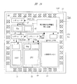
図9は、図8の半導体チップCHPに設けられた間欠動作基準電圧発生回路1におけるレイアウトの一例を示す説明図である。
FIG. 9 is an explanatory diagram showing an example of a layout in the intermittent operation reference
間欠動作基準電圧発生回路1は、図9の左上方に、バイアス回路2がレイアウトされており、その右側には、基準電圧発生回路3がレイアウトされている。基準電圧発生回路3の右側には、基準電圧生成回路4がレイアウトされている。
In the intermittent operation reference
バイアス回路2、および基準電圧発生回路3の下方には、低精度レファレンス回路8がレイアウトされており、該低精度レファレンス回路8の下方には、VOSCレギュレータ9がレイアウトされている。
A low
低精度レファレンス回路8、ならびにVOSCレギュレータ9の右側には、接続判定コンパレータ12がレイアウトされており、該接続判定コンパレータ12の右側には、接続用ディレイ13がレイアウトされている。
A
この接続用ディレイ13の右側には、アナログバッファ7がレイアウトされている。接続用ディレイ13、ならびにアナログバッファ7の下方には、保持容量回路6がレイアウトされており、該保持容量回路6の左側には、容量充電レギュレータ11がレイアウトされている。容量充電レギュレータ11の左側には、分周制御回路14がレイアウトされており、該分周制御回路14の左側には、発振回路5がレイアウトされている。
An
また、間欠動作基準電圧発生回路1がレイアウトされている外側には、該間欠動作基準電圧発生回路1を取り囲むようにガードリング24が形成されており、分周制御回路14、レベルシフタ10、および発振回路5の外側には、これら分周制御回路14、レベルシフタ10、および発振回路5を取り囲むようにガードリング25が形成されている。
In addition, a
さらに、レベルシフタ10の間には、該レベルシフタ10を2分割するようにガードリング26が形成されている。そして、これらガードリング24,25,26には、基準電位Vssがそれぞれ給電されている。
Further, a
間欠動作基準電圧発生回路1は、間欠動作を行うため発振回路5から生成される基準クロックCLKが存在する。この基準クロックCLKを、レベルシフタ10を介して分周制御回路14により分周、および波形制御を行っているが、発振回路5、レベルシフタ10、ならびに分周制御回路14のCMOS論理回路がスイッチング動作する際にノイズを発生する可能性がある。
The intermittent operation reference
したがって、バイアス回路2や基準電圧発生回路3などのノイズの影響を低減したい回路に対して、発振回路5、レベルシフタ10、ならびに分周制御回路14のような主要なノイズ発生源に基準電位Vssが給電されるガードリング25,26を設けることによりノイズ伝播を抑制する。
Therefore, the reference potential Vss is applied to the main noise generation sources such as the
また、間欠動作基準電圧発生回路1を囲むように形成されたガードリング24を設けることにより、間欠動作基準電圧発生回路1外部の近接する内部回路などにもスイッチングノイズの影響が伝播することを防止することができる。
Further, by providing the
さらに、間欠動作基準電圧発生回路1の上層には、図10に示すように、メタルシールド配線27,27aが形成されている。メタルシールド配線27は、メタルシールド配線27aと直交するようにメッシュ状にそれぞれ配線されている。
Further, as shown in FIG. 10,
このメタルシールド配線27,27aによって間欠動作基準電圧発生回路1の上層を覆うことにより、該間欠動作基準電圧発生回路1内部で発生するノイズを外部に伝播するのを防止するだけでなく、外部からのノイズの影響を軽減することができる。
By covering the upper layer of the intermittent operation reference
図11は、図9(図10)のA−B断面図である。 11 is a cross-sectional view taken along the line AB of FIG. 9 (FIG. 10).
たとえば、P型の半導体基板28の左上方には、DEEP−NWELL29が形成されており、このDEEP−NWELL29の上部には、左から右にかけて、NWELL30、PWELL31、およびNWELL32が形成されている。
For example, DEEP-
NWELL30の左側には、ガードリング25が形成されている。このガードリング25は、半導体基板28の上部に形成されたPWELL33、およびそのPWELL33の上部に形成されたP+型半導体領域34から構成されている。P+型半導体領域34は、PWELL33よりも不純物濃度の高い領域である。
A
NWELL32の右側には、半導体基板28の上部に形成されたPWELL35、ならびに該PWELL35の上部に形成されたP+型半導体領域36からなるガードリング26が形成されている。
On the right side of the
ガードリング26の右下方には、DEEP−NWELL37が形成されており、このDEEP−NWELL37の上部には、左から右にかけて、NWELL38、PWELL39、およびNWELL40が形成されている。
A DEEP-
NWELL40の右側には、半導体基板28の上部に形成されたPWELL41、およびそのPWELL41の上部に形成されたP+型半導体領域42からなるガードリング25が形成されている。
On the right side of the
このガードリング25の右下方には、DEEP−NWELL43が形成されており、該DEEP−NWELL43の上部には、左から右にかけて、NWELL44、PWELL45、NWELL46、PWELL47、ならびにNWELL48が形成されている。
A DEEP-
そして、NWELL48の右側には、半導体基板28の上部に形成されたPWELL49、ならびに該PWELL49の上部に形成されたP+型半導体領域50からなるガードリング24が形成されている。
On the right side of the
また、NWELL30とPWELL31の一部は、発振回路5を構成する半導体素子が形成される半導体素子形成領域となり、PWELL31の残りの部分、NWELL38、ならびにPWELL39の一部は、レベルシフタ10を構成する半導体素子が形成される半導体素子形成領域となる。
A part of NWELL 30 and
さらに、PWELL39の残りの部分、およびNWELL40は、分周制御回路14を構成する半導体素子が形成される半導体素子形成領域となり、NWELL44、PWELL45、およびNWELL46の一部は、容量充電レギュレータ11を構成する半導体素子が形成される半導体素子形成領域となる。
Further, the remaining part of the
そして、NWELL46の残りの部分、PWELL47、ならびにNWELL48は、保持容量回路6を構成する半導体素子が形成される半導体素子形成領域となる。
The remaining part of the
P+型半導体領域34,36,42,50は、ビア51を介して、たとえば、配線層MH1〜MH5のうち、第4の配線層MH4に形成されるメタルシールド配線27a、および該配線層MH4の上層である第5の配線層MH5に形成されるメタルシールド配線27に接続されている。
The P +
メタルシールド配線27,27aは、基準電位Vssに給電されており、メタルシールド配線27とメタルシールド配線27aとは、前述したように、それぞれが直交してメッシュ状となるように形成されている。
The
また、メタルシールド配線は、第4の配線層MH4と第5の配線層MH5の2つの配線層により構成するのではなく、たとえば、図12に示すように、1つの配線層でメッシュ状に、メタルシールド配線27を形成するようにしてもよい。
Further, the metal shield wiring is not constituted by two wiring layers of the fourth wiring layer MH4 and the fifth wiring layer MH5. For example, as shown in FIG. The
この場合、メタルシールド配線27は、図13に示すように、第4の配線層MH4にメッシュ状の配線を形成し、該メタルシールド配線27に基準電位Vssに給電する構成とする。また、その他の断面構成については、図11と同様であるので説明は省略する。
In this case, as shown in FIG. 13, the
さらに、ガードリングは、図14に示すように、間欠動作基準電圧発生回路1の外側に該間欠動作基準電圧発生回路1をすべて取り囲むように形成されるガードリング24と、発振回路5、レベルシフタ10、および分周制御回路14を取り囲むように形成されたガードリング25、レベルシフタ10を2分割するように形成されたガードリング26、およびガードリング25の外側を取り囲むように形成されたガードリング25aとを設け、発振回路5、レベルシフタ10、ならびに分周制御回路14を取り囲むガードリングを2重化する構成としてもよい。
Further, as shown in FIG. 14, the guard ring includes a
また、ガードリング24、およびガードリング25aは、基準電位Vssが給電されており、ガードリング25、ならびにガードリング26は、発振回路5の基準電位となる基準電位Vssoscが給電されている。これにより、ノイズによる悪影響をより効果的に低減することができる。
The
図15は、図14のA−B断面図である。 15 is a cross-sectional view taken along the line AB of FIG.
P型の半導体基板28の左側には、DEEP−NWELL29が形成されており、該DEEP−NWELL29の左上方には、PWELL52、およびそのPWELL52の上部に形成されたP+型半導体領域53から構成されているガードリング24が形成されている。このガードリング24には、基準電位Vssが給電されている。
A DEEP-
このガードリング24の右側には、PWELL54、および該PWELL54の上部に形成されたP+型半導体領域55から構成されているガードリング25が形成されている。ガードリング25には、基準電位Vssoscが給電される。
On the right side of the
ガードリング25の右側には、NWELL30、PWELL31、NWELL32を挟んで、基準電位Vssoscが給電されるガードリング26が形成されている。このガードリング26は、半導体基板28の上部に形成されたPWELL56、およびそのPWELL56の上部に形成されたP+型半導体領域57から構成されている。
A
また、ガードリング26の右側には、NWELL38、PWELL39、NWELL40を挟んで、ガードリング25が形成されている。このガードリング25は、半導体基板28の上部に形成されたPWELL58、およびそのPWELL58の上部に形成されたP+型半導体領域59から構成されている。
A
ガードリング25の右側には、基準電位Vssが給電されるガードリング25aが形成されている。このガードリング25aは、半導体基板28の上部に形成されたPWELL60、およびそのPWELL60の上部に形成されたP+型半導体領域61から構成されている。
On the right side of the
ガードリング25aの右側には、NWELL44、PWELL45、NWELL46、PWELL47、NWELL48を挟んで、ガードリング24が形成されている。ガードリング24は、半導体基板28の上部に形成されたPWELL62、およびそのPWELL62の上部に形成されたP+型半導体領域63から構成されている。
A
図16は、図1の間欠動作基準電圧発生回路1の構成に、保持電圧検知コンパレータ64を加えた一例を示すブロック図である。
FIG. 16 is a block diagram showing an example in which a holding
保持電圧検知コンパレータ64は、バイアス回路2から生成される、低精度のアナログレファレンス電圧信号CVREFより、保持容量回路6のレファレンス保持容量電圧POSTCHOLDの電圧レベルを比較し、低い場合には、極性信号FORCEONを反転させ強制的に基準電圧発生回路3、基準電圧生成回路4、ならびに容量充電レギュレータ11をONさせる。
The holding
このように、保持電圧検知コンパレータ64は、通常動作モード、およびスタンバイモード中に保持容量CHのレファレンス保持容量電圧POSTCHOLDのレベルが低いことを判断すると、チップ内外のなんらかの原因で、内部電源電圧Vintが内部回路の論理が不定となる電圧低下する前に、該内部電源電圧Vintのレファレンス電圧を本来の動作電圧まで復帰させる効果を有している。なお、消費電流は、図17に示すように、保持電圧検知コンパレータ64分が加算されることになる。
As described above, when the holding
なお、低精度のアナログレファレンス電圧信号CVREFは、CPU22などの内部回路で用いられるCMOS回路のPMOSトランジスタのしきい値Vthp、NMOSトランジスタのしきい値Vthn、しきい値の和(Vthp+Vthn)より高い電圧であるため、内部回路の論理が不確定になったかの判断基準となる。
The low-precision analog reference voltage signal CVREF is a voltage higher than the threshold value Vthp of the PMOS transistor, the threshold value Vthn of the NMOS transistor, and the sum of threshold values (Vthp + Vthn) used in the internal circuit such as the
それにより、本実施の形態によれば、消費電流の大きい基準電圧発生回路3、基準電圧生成回路4、ならびに容量充電レギュレータ11を間欠的にON/OFFさせることで、消費電流を大幅に低減させることができる。
Thereby, according to the present embodiment, the current consumption is significantly reduced by intermittently turning on / off the reference
(実施の形態2)
図18は、本発明の実施の形態2による間欠動作基準電圧発生回路の一例を示すブロック図、図19は、図18の間欠動作基準電圧発生回路を用いて構成した半導体チップにおけるレイアウトの一例を示す説明図、図20は、図18の間欠動作基準電圧発生回路による低消費電力効果の一例を示す説明図、図21は、図18の間欠動作基準電圧発生回路における状態遷移図である。
(Embodiment 2)
18 is a block diagram showing an example of an intermittent operation reference voltage generation circuit according to the second embodiment of the present invention. FIG. 19 shows an example of a layout in a semiconductor chip configured using the intermittent operation reference voltage generation circuit of FIG. FIG. 20 is an explanatory diagram showing an example of the low power consumption effect of the intermittent operation reference voltage generation circuit of FIG. 18, and FIG. 21 is a state transition diagram of the intermittent operation reference voltage generation circuit of FIG.
本実施の形態2において、間欠動作基準電圧発生回路1aは、図18に示すように、前記実施の形態1の図1の構成に、スイッチSW3〜SW6が新たに追加された構成となっている。図1では、レファレンス切り替え用のスイッチSW1,SW2により、レファレンス電圧VREFとして、基準電圧生成回路4の出力であるレファレンス電圧PREVREFか、アナログバッファ7の出力かを接続用ディレイ13から出力されるレファレンス切り替え信号CNTSWにより切り替えていた。
In the second embodiment, the intermittent operation reference voltage generation circuit 1a has a configuration in which switches SW3 to SW6 are newly added to the configuration of FIG. 1 of the first embodiment, as shown in FIG. . In FIG. 1, the reference switching is output from the
一方、図18では、レファレンス切り替え用のスイッチSW3〜SW6と、通常/スタンバイ状態選択信号ACT1,ACT2を利用し、保持容量CHに基準電圧発生回路3から出力されるレファレンス電圧PREVBGR,または基準電圧生成回路4の出力であるレファレンス電圧PREVREFのいずれかを保持する。
On the other hand, in FIG. 18, the reference voltage PREVBGR output from the reference
これにより、スタンバイモードとして、基準電圧発生回路3と基準電圧生成回路4とを間欠動作させるスタンバイ(間欠VREF)モードと、基準電圧発生回路3のみ間欠動作し、基準電圧生成回路4が常時ONとなるスタンバイ(間欠VBGR)モードを生成することができる。
Thereby, as a standby mode, a standby (intermittent VREF) mode in which the reference
このように、間欠動作基準電圧発生回路1aの構成により、スタンバイモードにおいても容量保持しないレファレンス電圧VREF2を利用することができる。 As described above, the configuration of the intermittent operation reference voltage generation circuit 1a makes it possible to use the reference voltage VREF2 that does not hold the capacity even in the standby mode.
図19は、間欠動作基準電圧発生回路1aが設けられた半導体集積回路装置における半導体チップCHPのレイアウトの一例を示す説明図である。 FIG. 19 is an explanatory diagram showing an example of the layout of the semiconductor chip CHP in the semiconductor integrated circuit device provided with the intermittent operation reference voltage generation circuit 1a.
正方形状の半導体チップCHPのそれぞれの外周辺部には、I/O領域15がレイアウトされている。I/O領域15より内側の右上方には、間欠動作基準電圧発生回路1aがレイアウトされている。
An I /
間欠動作基準電圧発生回路1aの左側には、レギュレータ17がレイアウトされており、その下方には、PLL18がレイアウトされており、該PLL8の右側には、電圧低下検知回路65(LVD3)がレイアウトされている。
The
PLL18の下方には、レギュレータ19がレイアウトされており、該レギュレータ19の右側には、レギュレータ20がレイアウトされている。そして、レギュレータ20の右側には、電圧低下検知回路66(LVD4)がレイアウトされている。
A
レギュレータ19の下方には、電圧低下検知回路67(LVD1)がレイアウトされており、該電圧低下検知回路67の下方には、RAM21がレイアウトされている。このRAM21の右側には、CPU22がレイアウトされている。
A voltage drop detection circuit 67 (LVD 1) is laid out below the
CPU22の上方には、レジスタ68、および電圧低下検知回路69(LVD2)がそれぞれレイアウトされている。CPU22の右側には、不揮発性メモリ23がレイアウトされている。
A
この図19に示すような構成では、半導体チップCHP内部の電源電圧(Vint,Vint_RAM,Vint_PLL)や外部電源電圧(Vext)を電圧低下検知回路65,66,67,69により通常動作モードだけでなく、電圧精度が通常動作時より劣化するがスタンバイモードにおいても電圧低下検知が行うことが可能となる。
In the configuration shown in FIG. 19, the power supply voltages (Vint, Vint_RAM, Vint_PLL) and the external power supply voltage (Vext) inside the semiconductor chip CHP are not only supplied to the normal operation mode by the voltage
なお、スタンバイ(間欠VREF)モードにおける低消費電流効果は図2のとおりであるが、スタンバイ(間欠VBGR)モードにおける低消費電流効果は、図20に示すようになる。 The low current consumption effect in the standby (intermittent VREF) mode is as shown in FIG. 2, but the low current consumption effect in the standby (intermittent VBGR) mode is as shown in FIG.
低消費電流効果は、基準電圧生成回路4が常時ONしている分スタンバイ(間欠VBGR)モードの方が小さい。また、通常動作モード、スタンバイ(間欠VREF)モード、スタンバイ(間欠VBGR)モード、およびオーバラップ状態の遷移は、図21に示す通りとなる。
The low current consumption effect is smaller in the standby (intermittent VBGR) mode because the reference
(実施の形態3)
図22は、本発明の実施の形態3による間欠動作基準電圧発生回路の一例を示すブロック図、図23は、図22の間欠動作基準電圧発生回路における状態遷移図、図24は、図22の間欠動作基準電圧発生回路による低消費電力効果の一例を示す説明図である。
(Embodiment 3)
22 is a block diagram showing an example of the intermittent operation reference voltage generation circuit according to the third embodiment of the present invention, FIG. 23 is a state transition diagram in the intermittent operation reference voltage generation circuit of FIG. 22, and FIG. It is explanatory drawing which shows an example of the low power consumption effect by an intermittent operation reference voltage generation circuit.
本実施の形態3においては、間欠動作基準電圧発生回路1bが、図22に示すように、前記実施の形態1の図1の構成からレファレンス切り替え用のスイッチSW1,SW2、接続判定コンパレータ12、ならびに接続用ディレイ13を取り除き、分周制御回路14の分周比切り替え信号FDSELと通常/スタンバイ状態選択信号ACTとのみで通常動作モードとスタンバイモード間の遷移を行う(図23)ものである。
In the third embodiment, as shown in FIG. 22, the intermittent operation reference voltage generating circuit 1b has the reference switching switches SW1 and SW2, the
接続判定コンパレータ12、および接続用ディレイ13は、スタンバイモードから通常動作モードに遷移する際に、アナログバッファ7の出力とレファレンス電圧PREVREFを通常/スタンバイ状態選択信号ACTの切り替えにより単純に接続してしまうとインピーダンスの違いにより出力電圧ドロップが生じることを回避するために使用されていたが、図22の回路構成の場合には、常にアナログバッファ7の出力がレファレンス電圧VREFの出力となっているため、接続判定コンパレータ12と接続用ディレイ13とを不要とすることができる。
The
これにより、図24に示すように、消費電流を低減することができるとともに、レファレンス電圧PREVREFとアナログバッファ7の出力とを切り換える際に生じる電圧ドロップを低減することができるので、オーバラップ期間を不要にすることができる。
As a result, as shown in FIG. 24, current consumption can be reduced, and voltage drop that occurs when switching between the reference voltage PREVREF and the output of the
(実施の形態4)
図25は、本発明の実施の形態4による間欠動作基準電圧発生回路の一例を示すブロック図、図26は、図25の間欠動作基準電圧発生回路による低消費電力効果の一例を示す説明図である。
(Embodiment 4)
FIG. 25 is a block diagram showing an example of the intermittent operation reference voltage generation circuit according to the fourth embodiment of the present invention, and FIG. 26 is an explanatory diagram showing an example of the low power consumption effect by the intermittent operation reference voltage generation circuit of FIG. is there.
本実施の形態4においては、間欠動作基準電圧発生回路1cが、図25に示すように、前記実施の形態3の図22の構成から、発振回路5の動作電圧VOSCを生成するVOSCレギュレータ9とレベルシフタ10とを削除した構成とし、発振回路5を外部電源電圧Vextで動作させている。
In the fourth embodiment, the intermittent operation reference voltage generating circuit 1c includes a
この構成は、システム電源に用いる間欠動作基準電圧発生回路1cを動作させる上で最小限必要な回路となる。このように、接続判定コンパレータ12、ならびに接続用ディレイ13だけでなく、VOSCレギュレータ9、レベルシフタ10も削除することで、これら回路の自己消費電流がなくなり、図26に示すように、スタンバイモード時の消費電流を低減する効果を大きくすることができる。
This configuration is a minimum circuit required for operating the intermittent operation reference voltage generating circuit 1c used for the system power supply. Thus, by deleting not only the
(実施の形態5)
図27は、本発明の実施の形態5による間欠動作基準電圧発生回路に設けられたバイアス回路の一例を示す回路図である。
(Embodiment 5)
FIG. 27 is a circuit diagram showing an example of a bias circuit provided in the intermittent operation reference voltage generating circuit according to the fifth embodiment of the present invention.
本実施の形態5においては、間欠動作基準電圧発生回路1(1a,1b、1c)に用いられるバイアス回路2の一例を示す。
In the fifth embodiment, an example of the
バイアス回路2は、図27に示すように、ワイドラー型電流源回路からなり、CMOSのトランジスタM0〜M3からなるカレントミラー回路と抵抗R0から定電流を生成する。
As shown in FIG. 27, the
定電流は、NBIASを介して間欠動作基準電圧発生回路1(1a,1b、1c)内の他回路へ供給される。一方、PMOSからなるトランジスタM4〜M7で構成される低精度のアナログレファレンス電圧信号CVREFは、ダイオード接続により飽和動作するPMOSのトランジスタM7のゲート−ソース間電圧Vgsがもつ負の温度依存性と、ゲートを基準電位Vss固定することにより線形動作するPMOSのトランジスタM5,M6のドレイン−ソース間電圧Vdsが持つ正の温度依存性を加算することにより、温度依存性を低減している。 The constant current is supplied to other circuits in the intermittent operation reference voltage generation circuit 1 (1a, 1b, 1c) via the NBIAS. On the other hand, the low-accuracy analog reference voltage signal CVREF composed of PMOS transistors M4 to M7 has a negative temperature dependency of the gate-source voltage Vgs of the PMOS transistor M7 that operates in saturation by diode connection, and the gate. By adding the positive temperature dependency of the drain-source voltage Vds of the PMOS transistors M5 and M6 that operate linearly by fixing the reference potential Vss, the temperature dependency is reduced.
なお、PMOSのトランジスタM5〜M7は、抵抗や寄生バイポーラ素子に比べプロセス変動の影響をうけやすいため、基準電圧発生回路3のようなトリミング前電圧精度は期待できない。
Note that the PMOS transistors M5 to M7 are more susceptible to process fluctuations than resistors and parasitic bipolar elements, and therefore the voltage accuracy before trimming as in the reference
また、トランジスタM10〜M17は、ワイドラー型電流源回路を起動させるスタートアップ回路である。ワイドラー型電流源回路は、自己バイアス回路構成であるため、リーク電流以外流れず回路動作しない安定状態と定電流を供給できる通常動作モードが存在する。スタートアップ回路は、外部電源電圧Vext投入後にバイアス回路2が前者の回路動作しない安定状態に陥ることを回避するためのものである。
Transistors M10 to M17 are start-up circuits that activate the wideler type current source circuit. Since the wideler type current source circuit has a self-bias circuit configuration, there exists a stable operation state in which the circuit does not operate except for leakage current and a normal operation mode in which constant current can be supplied. The start-up circuit is for preventing the
(実施の形態6)
図28は、本発明の実施の形態6による間欠動作基準電圧発生回路に設けられた基準電圧発生回路の一例を示す回路図である。
(Embodiment 6)
FIG. 28 is a circuit diagram showing an example of a reference voltage generation circuit provided in the intermittent operation reference voltage generation circuit according to the sixth embodiment of the present invention.
本実施の形態6においては、間欠動作基準電圧発生回路1(1a,1b、1c)に用いられる基準電圧発生回路3の一例を示す。
In the sixth embodiment, an example of the reference
基準電圧発生回路3は、図28に示すように、オペアンプAMP2がPNP寄生バイポーラのトランジスタQ10のベース−エミッタ間電圧Vbe10と抵抗R11と抵抗R12の中間電位が等しくなるように動作する。
As shown in FIG. 28, the reference
このとき、PNP寄生バイポーラのトランジスタQ10,Q11に流れる電流密度の差より、トランジスタQ10のベース−エミッタ間電圧Vbe10とトランジスタQ11のベース−エミッタ間電圧Vbe11に電位差△Vbeが生じるが、この電位差△Vbeは正の温度依存性を持つため、電位差△Vbeを抵抗比(R13/R11)倍した電圧とベース−エミッタ間電圧Vbe10自体が持つ負の温度依存性を加算することで、温度依存性の小さいレファレンス電圧PREVBGR=Vbe10+(R13/R11)×△Vbeが生成できる。 At this time, a potential difference ΔVbe occurs between the base-emitter voltage Vbe10 of the transistor Q10 and the base-emitter voltage Vbe11 of the transistor Q11 due to the difference in current density flowing in the PNP parasitic bipolar transistors Q10 and Q11. This potential difference ΔVbe Has a positive temperature dependence. Therefore, by adding the voltage obtained by multiplying the potential difference ΔVbe by the resistance ratio (R13 / R11) and the negative temperature dependence of the base-emitter voltage Vbe10 itself, the temperature dependence is small. The reference voltage PREVBGR = Vbe10 + (R13 / R11) × ΔVbe can be generated.
なお、PNP寄生バイポーラのトランジスタQ10,Q11は、標準CMOSプロセスで形成可能な素子であり、プロセスコストの増大はない。 The PNP parasitic bipolar transistors Q10 and Q11 are elements that can be formed by a standard CMOS process and do not increase the process cost.
(実施の形態7)
図29は、本発明の実施の形態7による間欠動作基準電圧発生回路に設けられた基準電圧発生回路の一例を示す回路図である。
(Embodiment 7)
FIG. 29 is a circuit diagram showing an example of a reference voltage generation circuit provided in the intermittent operation reference voltage generation circuit according to the seventh embodiment of the present invention.
本実施の形態7においては、前記実施の形態6に示した基準電圧発生回路3における他の構成例を示す。
The seventh embodiment shows another configuration example of the reference
この場合、基準電圧発生回路3は、図29に示すように、寄生バイポーラトランジスタとしてNPN型のトランジスタQ1〜Q3を用い、かつ寄生NPNのトランジスタQ1,Q2を3端子素子として利用することで、オペアンプAMP0,AMP1の入力電圧オフセットを低減し、レファレンス電圧PREVBGRのトリミング前電圧精度を向上することのできる回路構成となっている。
In this case, as shown in FIG. 29, the reference
これは、図28の基準電圧発生回路3と同じくオペアンプAMP0,AMP1からNPN型のトランジスタQ1,Q2のベース−エミッタ間電圧△Vbeを抵抗R1により取り出すが、トランジスタQ1,Q2のコレクタ側で電圧比較を行うため、結果としてコレクタ電流Icとベース電流Ibの比hfe=Ic/Ib分入力電圧オフセットが低減されることになる。
As in the reference
なお、hfe比の大きな寄生NPNバイポーラトランジスタを構成するには、コレクタをDEEP−NWELLで形成することが多く、標準CMOSプロセスに、該DEEP−NWELLを加えた3重ウェル構造のCMOSプロセスが必要となってくる。 In order to construct a parasitic NPN bipolar transistor having a large hfe ratio, the collector is often formed of DEEP-NWELL, and a CMOS process with a triple well structure in which DEEP-NWELL is added to the standard CMOS process is required. It becomes.
DEEP−NWELLを追加することはプロセスコスト増であるが、このDEEP−NWELLをI/O領域に用いられるトランジスタのESD(静電気放電)保護用素子の一部として利用したり、基板ノイズ分離のためADC(アナログ/デジタル変換)などのチップ内モジュールで用いたりするなど一般的に用いられることが多く、基準電圧発生回路3の電圧精度向上のため寄生NPNトランジスタが用いられることも多い。
Adding DEEP-NWELL increases the process cost, but this DEEP-NWELL can be used as part of an ESD (electrostatic discharge) protection element for transistors used in the I / O region, or for substrate noise isolation. In many cases, it is generally used such as in an in-chip module such as ADC (analog / digital conversion), and a parasitic NPN transistor is often used to improve the voltage accuracy of the reference
(実施の形態8)
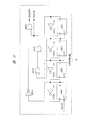
図30は、本発明の実施の形態8による間欠動作基準電圧発生回路に設けられた基準電圧生成回路の一例を示す回路図である。
(Embodiment 8)
FIG. 30 is a circuit diagram showing an example of a reference voltage generation circuit provided in the intermittent operation reference voltage generation circuit according to the eighth embodiment of the present invention.
本実施の形態8においては、間欠動作基準電圧発生回路1(1a,1b、1c)に用いられる基準電圧生成回路4の一例を示す。
In the eighth embodiment, an example of the reference
基準電圧生成回路4は、図30に示すように、オペアンプAMP10、トランジスタM60,M70〜M72、論理和回路OR2、スイッチSW10〜SW12、および抵抗R50〜R63,R70〜R72,R80〜R83,R90〜R93からなる。
As shown in FIG. 30, the reference
基準電圧生成回路4は、基準電圧発生回路3などの出力電圧を入力電圧VINとして抵抗比により電圧変換し、チップに必要なレファレンス電圧PREVREF,VREF2を生成する回路である。
The reference
なお、このレファレンス電圧の調整はiビットのトリミング信号TRIMにより、抵抗分圧比を調整することで行われる。 The reference voltage is adjusted by adjusting the resistance voltage dividing ratio by an i-bit trimming signal TRIM.
(実施の形態9)
図31は、本発明の実施の形態9による間欠動作基準電圧発生回路に設けられた発振回路の一例を示す回路図である。
(Embodiment 9)
FIG. 31 is a circuit diagram showing an example of an oscillation circuit provided in the intermittent operation reference voltage generating circuit according to the ninth embodiment of the present invention.
本実施の形態9においては、間欠動作基準電圧発生回路1(1a,1b、1c)に用いられる発振回路5における構成の一例を示す。
In the ninth embodiment, an example of the configuration of the
発振回路5は、図31に示すように、トランジスタM80〜M89,M90〜M95,M100〜M105,M110,M111、静電容量素子C0〜C3、およびインバータINV0,INV1からなり、奇数段(図31では5段)のインバータ回路からなるリングオシレータで構成され、バイアス回路2で決められる定電流と、VOSCレギュレータ9が生成する発振回路5の動作電圧である動作電圧VOSC、および静電容量素子C0〜C3の値により生成する基準クロックCLKの発振周波数が決定される。
As shown in FIG. 31, the
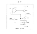
(実施の形態10)
図32は、本発明の実施の形態10による間欠動作基準電圧発生回路に設けられた分周制御回路の一例を示す回路図、図33は、図32の分周制御回路における動作波形の一例を示すタイミングチャートである。
(Embodiment 10)
32 is a circuit diagram showing an example of a frequency division control circuit provided in the intermittent operation reference voltage generation circuit according to the tenth embodiment of the present invention, and FIG. 33 shows an example of an operation waveform in the frequency division control circuit of FIG. It is a timing chart which shows.
本実施の形態10においては、間欠動作基準電圧発生回路1(1a,1b、1c)に用いられる分周制御回路14における構成の一例を示す。
In the tenth embodiment, an example of the configuration of the frequency
分周制御回路14は、図32に示すように、発振回路5が生成した基準クロックCLK、またはこの基準クロックCLKをレベルシフタ10により電圧振幅を変換したクロックCLK_UPをエッジトリガDフリップフロップからなるフリップフロップDFF0〜DFF3とインバータINV20〜INV23からなる分周回路で分周した後、論理回路(インバータINV11、および論理積回路AND0〜AND2)により、イネーブル信号VREFON、ならびにサンプリング/ホールド信号CHOLDSWを生成する。
As shown in FIG. 32, the frequency
また、図33に分周制御回路14の動作波形例を示す。なお、この図33においては、クロックCLKINを16分周し、イネーブル信号VREFONがHiレベルとなる2クロック期間と、保持容量CHに電圧をチャージするためサンプリング/ホールド信号CHOLDSWをHiレベルとする1クロック期間を生成するとともに、14クロック期間はイネーブル信号VREFONなどをOFFすることで、基準電圧発生回路3、および基準電圧生成回路4のON/OFF期間は1/8分周動作となっている。
FIG. 33 shows an example of operation waveforms of the frequency
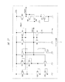
(実施の形態11)
図34は、本発明の実施の形態11による間欠動作基準電圧発生回路に設けられた低精度レファレンス回路の一例を示す回路図、図35は、本発明の実施の形態11による間欠動作基準電圧発生回路に設けられた接続用ディレイの一例を示す回路図である。
(Embodiment 11)
FIG. 34 is a circuit diagram showing an example of a low-precision reference circuit provided in the intermittent operation reference voltage generation circuit according to the eleventh embodiment of the present invention, and FIG. 35 shows the intermittent operation reference voltage generation according to the eleventh embodiment of the present invention. It is a circuit diagram which shows an example of the delay for a connection provided in the circuit.
本実施の形態11においては、間欠動作基準電圧発生回路1(1a,1b、1c)に用いられる低精度レファレンス回路8における構成の一例を示す。
In the eleventh embodiment, an example of the configuration of the low-
低精度レファレンス回路8は、図34に示すように、オペアンプAMP20、トランジスタM140,M150〜M152から構成されている。
As shown in FIG. 34, the low-
この場合、低精度レファレンス回路8は、基準電圧生成回路4に類似の回路であるが、高い電圧精度を求められていないこと、入力電圧VINとして入力される低精度のアナログレファレンス電圧信号CVREFの2倍程度の電圧をレファレンス電圧CVREF2として生成できればよいので、ダイオード接続したMOSのトランジスタM151,M152などを抵抗の代わりとして用いることで、低消費電流で面積の小さい回路を実現している。
In this case, the low-
また、図35は、間欠動作基準電圧発生回路1(1a,1b、1c)に用いられる接続用ディレイ13における構成の一例を示した回路図である。
FIG. 35 is a circuit diagram showing an example of the configuration of the
接続用ディレイ13は、アナログ、またはデジタルディレイ回路かその両方で構成されており、図35は、アナログまたはデジタルディレイ回路の両方を含むものである。
The
アナログディレイ回路は、図35におけるCMOSのトランジスタM140〜M145、インバータINV43,INV44、および静電容量素子C10から構成され、アナログレファレンス信号NBIASの定電流を元に、静電容量素子C10に電荷を充電し、インバータINV43の論理しきい値を超えるまでの期間の遅延時間が得られるものである。 The analog delay circuit includes CMOS transistors M140 to M145, inverters INV43 and INV44, and a capacitive element C10 in FIG. 35, and charges the capacitive element C10 based on the constant current of the analog reference signal NBIAS. In addition, a delay time of a period until the logic threshold value of the inverter INV43 is exceeded can be obtained.
一方、デジタルディレイ回路は、エッジトリガDフリップフロップからなるフリップフロップDFF20,DFF21と論理回路(インバータINV41,INV42、および論理積回路AND11)から構成されており、入力クロックCLKINを元に遅延時間を生成するものである。 On the other hand, the digital delay circuit is composed of flip-flops DFF20 and DFF21 that are edge trigger D flip-flops and a logic circuit (inverters INV41 and INV42, and an AND circuit AND11), and generates a delay time based on the input clock CLKIN. To do.
これらのディレイ期間を利用し、スタンバイモードから通常動作モードへの遷移時の電圧ドロップの発生を低減する。なお、アナログディレイを用いるかデジタルディレイを用いるかは、通常動作モード時に発振回路5が動作中かどうかで切り替わる仕組みとなっている。
By using these delay periods, the occurrence of voltage drop during transition from the standby mode to the normal operation mode is reduced. Note that whether the analog delay or the digital delay is used is switched depending on whether or not the
以上、本発明者によってなされた発明を実施の形態に基づき具体的に説明したが、本発明は前記実施の形態に限定されるものではなく、その要旨を逸脱しない範囲で種々変更可能であることはいうまでもない。 As mentioned above, the invention made by the present inventor has been specifically described based on the embodiment. However, the present invention is not limited to the embodiment, and various modifications can be made without departing from the scope of the invention. Needless to say.
本発明は、レファレンス電圧を生成するレファレンス電圧生成回路を有する半導体集積回路装置に適している。 The present invention is suitable for a semiconductor integrated circuit device having a reference voltage generation circuit that generates a reference voltage.
1 間欠動作基準電圧発生回路
1a 間欠動作基準電圧発生回路
1b 間欠動作基準電圧発生回路
1c 間欠動作基準電圧発生回路
2 バイアス回路
3 基準電圧発生回路
4 基準電圧生成回路
5 発振回路
6 保持容量回路
7 アナログバッファ
8 低精度レファレンス回路
9 VOSCレギュレータ
10 レベルシフタ
11 容量充電レギュレータ
12 接続判定コンパレータ
13 接続用ディレイ
14 分周制御回路
15 I/O領域
16 システム電源回路
17 レギュレータ
18 PLL
19 レギュレータ
20 レギュレータ
21 RAM
22 CPU
23 不揮発性メモリ
24 ガードリング
25 ガードリング
25a ガードリング
26 ガードリング
27 メタルシールド配線
27a メタルシールド配線
28 半導体基板
29 DEEP−NWELL
30 NWELL
31 PWELL
32 NWELL
33 PWELL
34 P+型半導体領域
35 PWELL
36 P+型半導体領域
37 DEEP−NWELL
38 NWELL
39 PWELL
40 NWELL
41 PWELL
42 P+型半導体領域
43 DEEP−NWELL
44 NWELL
45 PWELL
46 NWELL
47 PWELL
48 NWELL
49 PWELL
50 P+型半導体領域
51 ビア
52 PWELL
53 P+型半導体領域
54 PWELL
55 P+型半導体領域
56 PWELL
57 P+型半導体領域
58 PWELL
59 P+型半導体領域
60 PWELL
61 P+型半導体領域
62 PWELL
63 P+型半導体領域
64 保持電圧検知コンパレータ
65 電圧低下検知回路
66 電圧低下検知回路
67 電圧低下検知回路
68 レジスタ
69 電圧低下検知回路
M1〜M7 トランジスタ
M10〜M17 トランジスタ
M60 トランジスタ
M70〜M72 トランジスタ
M80〜M89 トランジスタ
M90〜M95 トランジスタ
M100〜M105 トランジスタ
M110〜M112 トランジスタ
M140 トランジスタ
M150〜M152 トランジスタ
Q1〜Q3 トランジスタ
Q10,Q11 トランジスタ
CH 保持容量
SWH スイッチ
SW1〜SW6 スイッチ
CHP 半導体チップ
MH1〜MH5 配線層
R0,R11,R12 抵抗
R50〜R63 抵抗
R70〜R72 抵抗
R80〜R83 抵抗
R90〜R93 抵抗
AMP0〜AMP2 オペアンプ
AMP10,AMP20 オペアンプ
OR2 論理和回路
C0 静電容量素子
INV0,INV1 インバータ
INV20〜INV23 インバータ
INV41〜INV44 インバータ
DFF0〜DFF3 フリップフロップ
DFF20,DFF21 フリップフロップ
AND0〜AND2,AND11 論理積回路
C10 静電容量素子
1 intermittent operation reference voltage generation circuit 1a intermittent operation reference voltage generation circuit 1b intermittent operation reference voltage generation circuit 1c intermittent operation reference
19
22 CPU
23
30 NWELL
31 PWELL
32 NWELL
33 PWELL
34 P +
36 P +
38 NWELL
39 PWELL
40 NWELL
41 PWELL
42 P +
44 NWELL
45 PWELL
46 NWELL
47 PWELL
48 NWELL
49 PWELL
50 P +
53 P +
55 P +
57 P + type semiconductor region 58 PWELL
59 P +
61 P +
63 P +
Claims (7)
前記レファレンス電圧生成手段は、
前記レファレンス電圧を生成するレファレンス電圧生成部と、
低消費電力モードの1つであるスタンバイモード時に、前記レファレンス電圧生成部を間欠動作させて前記レファレンス電圧を生成する間欠動作制御部とを備え、
前記間欠動作制御部は、
基準クロック信号を任意の分周信号に変換し、第1の制御信号、および第2の制御信号を生成する制御信号生成部と、
前記スタンバイモード時に、前記第1の制御信号に基づいて動作し、前記レファレンス電圧生成部が生成したレファレンス電圧を安定化させる充電用レギュレータと、
前記充電用レギュレータが安定化させた電源電圧を、前記第2の制御信号に基づいて、サンプル/ホールドするサンプル/ホールド回路と、
前記サンプル/ホールド回路の電源電圧をバッファして前記レファレンス電圧として出力するバッファ部と、
前記スタンバイモード時に、前記レファレンス電圧生成部と前記レファレンス電圧生成手段の出力部とを非導通状態とし、前記バッファ部と前記出力部とを導通状態として前記バッファ部から出力される電源電圧をレファレンス電圧として出力するスイッチ部とを備え、
前記レファレンス電圧生成部は、
前記制御信号生成部が生成する前記第1の制御信号に基づいて間欠動作することを特徴とする半導体集積回路装置。 A semiconductor integrated circuit device comprising reference voltage generating means for generating a reference voltage,
The reference voltage generating means includes
A reference voltage generator for generating the reference voltage;
An intermittent operation control unit that generates the reference voltage by intermittently operating the reference voltage generation unit in a standby mode that is one of the low power consumption modes ;
The intermittent operation controller is
A control signal generating unit that converts the reference clock signal into an arbitrary divided signal and generates a first control signal and a second control signal;
A charging regulator that operates based on the first control signal in the standby mode and stabilizes the reference voltage generated by the reference voltage generator;
A sample / hold circuit that samples / holds the power supply voltage stabilized by the charging regulator based on the second control signal;
A buffer unit that buffers the power supply voltage of the sample / hold circuit and outputs the buffered voltage as the reference voltage;
In the standby mode, the reference voltage generation unit and the output unit of the reference voltage generation unit are in a non-conductive state, the buffer unit and the output unit are in a conductive state, and the power supply voltage output from the buffer unit is a reference voltage. And a switch unit that outputs as
The reference voltage generator is
A semiconductor integrated circuit device, wherein the semiconductor integrated circuit device operates intermittently based on the first control signal generated by the control signal generator .
前記間欠動作制御部は、The intermittent operation controller is
前記制御信号生成部に供給する基準クロック信号を生成する発振回路を備えたことを特徴とする半導体集積回路装置。A semiconductor integrated circuit device comprising an oscillation circuit that generates a reference clock signal to be supplied to the control signal generation unit.
前記間欠動作制御部は、The intermittent operation controller is
外部供給される外部電源電圧を降圧した発振用電源電圧を生成し、前記発振回路に電源電圧として供給する発振回路用レギュレータを備えたことを特徴とする半導体集積回路装置。A semiconductor integrated circuit device comprising: an oscillation circuit regulator that generates an oscillation power supply voltage obtained by stepping down an external power supply voltage supplied externally and supplies the oscillation circuit with the oscillation power supply voltage.
前記間欠動作制御部は、The intermittent operation controller is
前記スタンバイモードから通常動作モードに遷移した際に、前記レファレンス電圧生成部から出力されるレファレンス電圧の上昇を検知して任意の遅延時間が経過した後にスイッチ制御信号を出力し、前記レファレンス電圧生成部と前記レファレンス電圧生成手段の前記出力部とが導通状態となり、前記バッファ部と前記出力部とが非導通状態となるように前記スイッチ部を切り換える接続切り換え制御部を備えたことを特徴とする半導体集積回路装置。When a transition from the standby mode to the normal operation mode is performed, an increase in the reference voltage output from the reference voltage generation unit is detected, and after an arbitrary delay time has elapsed, a switch control signal is output, and the reference voltage generation unit And a connection switching control section for switching the switch section so that the output section of the reference voltage generating means is in a conductive state and the buffer section and the output section are in a non-conductive state. Integrated circuit device.
前記レファレンス電圧生成部は、The reference voltage generator is
トリミング信号により、生成するレファレンス電圧を調整することのできる機能を有し、前記スタンバイモードに移行した際に、前記トリミング信号による調整を行うリセット期間中に間欠動作しないことを特徴とする半導体集積回路装置。A semiconductor integrated circuit having a function capable of adjusting a reference voltage to be generated by a trimming signal, and not operating intermittently during a reset period in which the adjustment by the trimming signal is performed when shifting to the standby mode apparatus.
前記レファレンス電圧生成手段は、The reference voltage generating means includes
前記レファレンス電圧生成手段の周囲が取り囲まれるようにガードリングが形成されていることを特徴とする半導体集積回路装置。A semiconductor integrated circuit device, wherein a guard ring is formed so as to surround the reference voltage generating means.
前記レファレンス電圧生成手段は、The reference voltage generating means includes
前記レファレンス電圧生成手段が形成された上方を覆うようにメッシュ状のメタルシールド配線が形成されていることを特徴とする半導体集積回路装置。A semiconductor integrated circuit device, wherein a mesh-shaped metal shield wiring is formed so as to cover an upper portion where the reference voltage generating means is formed.
Priority Applications (2)
| Application Number | Priority Date | Filing Date | Title |
|---|---|---|---|
| JP2009153702A JP5412190B2 (en) | 2009-06-29 | 2009-06-29 | Semiconductor integrated circuit device |
| US12/796,033 US20100327841A1 (en) | 2009-06-29 | 2010-06-08 | Semiconductor integrated circuit device |
Applications Claiming Priority (1)
| Application Number | Priority Date | Filing Date | Title |
|---|---|---|---|
| JP2009153702A JP5412190B2 (en) | 2009-06-29 | 2009-06-29 | Semiconductor integrated circuit device |
Publications (3)
| Publication Number | Publication Date |
|---|---|
| JP2011008683A JP2011008683A (en) | 2011-01-13 |
| JP2011008683A5 JP2011008683A5 (en) | 2012-05-24 |
| JP5412190B2 true JP5412190B2 (en) | 2014-02-12 |
Family
ID=43379947
Family Applications (1)
| Application Number | Title | Priority Date | Filing Date |
|---|---|---|---|
| JP2009153702A Expired - Fee Related JP5412190B2 (en) | 2009-06-29 | 2009-06-29 | Semiconductor integrated circuit device |
Country Status (2)
| Country | Link |
|---|---|
| US (1) | US20100327841A1 (en) |
| JP (1) | JP5412190B2 (en) |
Families Citing this family (9)
| Publication number | Priority date | Publication date | Assignee | Title |
|---|---|---|---|---|
| JP5695439B2 (en) * | 2011-02-18 | 2015-04-08 | ルネサスエレクトロニクス株式会社 | Semiconductor device |
| JP6120528B2 (en) * | 2012-11-08 | 2017-04-26 | ルネサスエレクトロニクス株式会社 | Semiconductor device and manufacturing method thereof |
| JP2015069019A (en) | 2013-09-30 | 2015-04-13 | シナプティクス・ディスプレイ・デバイス株式会社 | Semiconductor device |
| KR102190453B1 (en) * | 2014-02-17 | 2020-12-11 | 삼성전자주식회사 | Power management device and system on chip including the same |
| JP6492507B2 (en) | 2014-10-06 | 2019-04-03 | 株式会社デンソー | Electronic control unit |
| JP5888387B1 (en) * | 2014-10-22 | 2016-03-22 | ミツミ電機株式会社 | Battery protection circuit, battery protection device, and battery pack |
| KR20170007036A (en) | 2015-07-10 | 2017-01-18 | 에스케이하이닉스 주식회사 | Input Circuit and Semiconductor Apparatus Having the Same |
| CN113448458A (en) * | 2020-03-25 | 2021-09-28 | 昇佳电子股份有限公司 | Capacitance sensing circuit |
| US11404129B1 (en) * | 2021-02-05 | 2022-08-02 | Micron Technology, Inc. | Power architecture for non-volatile memory |
Family Cites Families (11)
| Publication number | Priority date | Publication date | Assignee | Title |
|---|---|---|---|---|
| JP3318365B2 (en) * | 1992-10-20 | 2002-08-26 | 富士通株式会社 | Constant voltage circuit |
| JPH09288897A (en) * | 1996-04-19 | 1997-11-04 | Sony Corp | Voltage supplying circuit |
| US5959471A (en) * | 1997-09-25 | 1999-09-28 | Siemens Aktiengesellschaft | Method and apparatus for reducing the bias current in a reference voltage circuit |
| JP3293584B2 (en) * | 1999-03-02 | 2002-06-17 | 日本電気株式会社 | Reference voltage generator and method |
| JP3398693B2 (en) * | 1999-08-24 | 2003-04-21 | エヌイーシーマイクロシステム株式会社 | Semiconductor storage device |
| JP2002091591A (en) * | 2000-09-14 | 2002-03-29 | Seiko Epson Corp | Device for outputting constant voltage |
| GB2376081B (en) * | 2001-03-14 | 2004-12-08 | Micron Technology Inc | Measurement of the integrity of a power supply |
| JP2003005844A (en) * | 2001-06-25 | 2003-01-08 | Matsushita Electric Ind Co Ltd | Low consumption current type regulator circuit |
| TW200524139A (en) * | 2003-12-24 | 2005-07-16 | Renesas Tech Corp | Voltage generating circuit and semiconductor integrated circuit |
| JP5067836B2 (en) * | 2005-12-19 | 2012-11-07 | ルネサスエレクトロニクス株式会社 | Nonvolatile semiconductor memory device and operation method thereof |
| JP5460093B2 (en) * | 2009-03-26 | 2014-04-02 | ラピスセミコンダクタ株式会社 | Internal power control circuit for semiconductor memory and semiconductor device |
-
2009
- 2009-06-29 JP JP2009153702A patent/JP5412190B2/en not_active Expired - Fee Related
-
2010
- 2010-06-08 US US12/796,033 patent/US20100327841A1/en not_active Abandoned
Also Published As
| Publication number | Publication date |
|---|---|
| US20100327841A1 (en) | 2010-12-30 |
| JP2011008683A (en) | 2011-01-13 |
Similar Documents
| Publication | Publication Date | Title |
|---|---|---|
| JP5412190B2 (en) | Semiconductor integrated circuit device | |
| Yang et al. | A nanosecond-transient fine-grained digital LDO with multi-step switching scheme and asynchronous adaptive pipeline control | |
| US8136987B2 (en) | Ratio meter for temperature sensor | |
| US7528590B2 (en) | DC/DC boost converter with pulse skipping circuitry | |
| US7768242B2 (en) | DC/DC boost converter with resistorless current sensing | |
| US7873854B2 (en) | System for monitoring power supply voltage | |
| US7107178B2 (en) | Temperature sensing circuit for use in semiconductor integrated circuit | |
| US7852061B2 (en) | Band gap generator with temperature invariant current correction circuit | |
| US7622963B2 (en) | General purpose comparator with multiplexer inputs | |
| JP2004133800A (en) | Semiconductor integrated circuit device | |
| US20090089599A1 (en) | Power supply system for low power mcu | |
| US8710913B2 (en) | Circuit arrangement and method for operating a circuit arrangement | |
| US20140145707A1 (en) | Voltage fluctuation detection circuit and semiconductor integrated circuit | |
| US10637476B2 (en) | Clock integrated circuit | |
| US10788376B2 (en) | Apparatus for sensing temperature in electronic circuitry and associated methods | |
| US7123105B2 (en) | Oscillator with temperature control | |
| US7135913B2 (en) | Reference voltage generating circuit for integrated circuit | |
| US9922699B1 (en) | Adaptive diode sizing techniques for reducing memory power leakage | |
| KR100534157B1 (en) | Semiconductor integrated device, methods of detecting and correcting a voltage drop in an integrated circuit | |
| US9792979B1 (en) | Process, voltage, and temperature tracking SRAM retention voltage regulator | |
| US7602168B2 (en) | Voltage regulator for integrated circuits | |
| Kim et al. | An ultra-low voltage digitally controlled low-dropout regulator with digital background calibration | |
| CN114174789A (en) | Reversed bandgap reference circuit with body effect diode and switched capacitor temperature sensor with duty cycle output | |
| US10126773B2 (en) | Circuit and method for providing a secondary reference voltage from an initial reference voltage | |
| Kim et al. | PVT variation tolerant current source with on-chip digital self-calibration |
Legal Events
| Date | Code | Title | Description |
|---|---|---|---|
| A521 | Request for written amendment filed |
Free format text: JAPANESE INTERMEDIATE CODE: A523 Effective date: 20120321 |
|
| A621 | Written request for application examination |
Free format text: JAPANESE INTERMEDIATE CODE: A621 Effective date: 20120321 |
|
| A977 | Report on retrieval |
Free format text: JAPANESE INTERMEDIATE CODE: A971007 Effective date: 20130718 |
|
| A131 | Notification of reasons for refusal |
Free format text: JAPANESE INTERMEDIATE CODE: A131 Effective date: 20130723 |
|
| A521 | Request for written amendment filed |
Free format text: JAPANESE INTERMEDIATE CODE: A523 Effective date: 20130920 |
|
| A01 | Written decision to grant a patent or to grant a registration (utility model) |
Free format text: JAPANESE INTERMEDIATE CODE: A01 Effective date: 20131015 |
|
| A61 | First payment of annual fees (during grant procedure) |
Free format text: JAPANESE INTERMEDIATE CODE: A61 Effective date: 20131111 |
|
| S531 | Written request for registration of change of domicile |
Free format text: JAPANESE INTERMEDIATE CODE: R313531 |
|
| R350 | Written notification of registration of transfer |
Free format text: JAPANESE INTERMEDIATE CODE: R350 |
|
| LAPS | Cancellation because of no payment of annual fees |