JP5407918B2 - Reflection detection device, display device, electronic device, and reflection detection method - Google Patents
Reflection detection device, display device, electronic device, and reflection detection method Download PDFInfo
- Publication number
- JP5407918B2 JP5407918B2 JP2010028845A JP2010028845A JP5407918B2 JP 5407918 B2 JP5407918 B2 JP 5407918B2 JP 2010028845 A JP2010028845 A JP 2010028845A JP 2010028845 A JP2010028845 A JP 2010028845A JP 5407918 B2 JP5407918 B2 JP 5407918B2
- Authority
- JP
- Japan
- Prior art keywords
- light
- detection light
- detection
- emission
- display
- Prior art date
- Legal status (The legal status is an assumption and is not a legal conclusion. Google has not performed a legal analysis and makes no representation as to the accuracy of the status listed.)
- Expired - Fee Related
Links
Images


Classifications
-
- G—PHYSICS
- G06—COMPUTING OR CALCULATING; COUNTING
- G06F—ELECTRIC DIGITAL DATA PROCESSING
- G06F3/00—Input arrangements for transferring data to be processed into a form capable of being handled by the computer; Output arrangements for transferring data from processing unit to output unit, e.g. interface arrangements
- G06F3/01—Input arrangements or combined input and output arrangements for interaction between user and computer
- G06F3/03—Arrangements for converting the position or the displacement of a member into a coded form
- G06F3/041—Digitisers, e.g. for touch screens or touch pads, characterised by the transducing means
- G06F3/042—Digitisers, e.g. for touch screens or touch pads, characterised by the transducing means by opto-electronic means
-
- G—PHYSICS
- G06—COMPUTING OR CALCULATING; COUNTING
- G06F—ELECTRIC DIGITAL DATA PROCESSING
- G06F3/00—Input arrangements for transferring data to be processed into a form capable of being handled by the computer; Output arrangements for transferring data from processing unit to output unit, e.g. interface arrangements
- G06F3/01—Input arrangements or combined input and output arrangements for interaction between user and computer
- G06F3/03—Arrangements for converting the position or the displacement of a member into a coded form
- G06F3/0304—Detection arrangements using opto-electronic means
Landscapes
- Engineering & Computer Science (AREA)
- General Engineering & Computer Science (AREA)
- Theoretical Computer Science (AREA)
- Human Computer Interaction (AREA)
- Physics & Mathematics (AREA)
- General Physics & Mathematics (AREA)
- Position Input By Displaying (AREA)
Description
光出射面(表示装置では表示面)から外部に検出光を出射し、その反射検出光を複数の受光素子で受光する反射検出装置と、反射検出方法とに関する。また、本発明は、上記反射検出の機能を有する表示装置および電子機器に関する。 The present invention relates to a reflection detection device that emits detection light to the outside from a light emission surface (display surface in a display device) and receives the reflection detection light by a plurality of light receiving elements, and a reflection detection method. The present invention also relates to a display device and an electronic apparatus having the above-described reflection detection function.
反射検出は、一般に、物体に光を出射し、その反射光により物体の有無を検出するものである。
しかし、単に物体の有無にとどまらず、物体の面内位置を検出する位置検出にも反射検出が用いられることがある。
In reflection detection, light is generally emitted to an object, and the presence or absence of the object is detected by the reflected light.
However, not only the presence / absence of an object but also reflection detection may be used for position detection for detecting the in-plane position of the object.
例えば指示位置検出のための受光素子を表示パネルに内蔵した、光学式の位置検出機能を備える表示装置が知られている(例えば、特許文献1参照)。
上記特許文献1に記載された技術では、液晶パネルまたは有機ELパネルなどの表示パネルに、画面の一部の画素あるいは全画素に光を感知するセンサ(受光素子)を配置している。センサからの検出信号を、当該センサが設けられた画素の位置情報と対応付けると、パネル表面に接触した指やペンなどの物体の面内位置を検出できる。この物体に照射しセンサで感知する光は、赤外(IR)光などの非可視光が用いられている。非可視光を用いると黒表示など画面領域でも位置検出が可能である。
For example, a display device having an optical position detection function in which a light receiving element for detecting an indicated position is built in a display panel is known (for example, see Patent Document 1).
In the technique described in
これに対し、検出光の出射面から物体までの距離の測定は、カメラ装置の自動焦点合わせなどの目的で行う三角測量法などが知られている。 On the other hand, the measurement of the distance from the exit surface of the detection light to the object is a triangulation method or the like performed for the purpose of automatic focusing of the camera device.
しかし、一般の距離測定法は、ある狙った範囲に光を照準させなければならないため、大きな面内のどの位置でも距離測定ができるわけではない。その理由から、タッチパネルやタッチセンサ内蔵の表示装置は、三角測量法を用いて表示面からの距離(高さ)測定ができない。 However, since a general distance measurement method requires light to be aimed at a certain target range, distance measurement cannot be performed at any position in a large plane. For this reason, a display device with a built-in touch panel or touch sensor cannot measure the distance (height) from the display surface using the triangulation method.
本発明は、光出射面からの距離(高さ)を測定することが可能な位置検出装置を提供する。
本発明は、当該位置検出装置の機能を有し、表示面からの距離(高さ)を測定できる表示装置と、表示装置を有する電子機器とを提供する。
本発明は、光出射面からの距離(高さ)を測定することが可能な位置検出方法を提供する。
The present invention provides a position detection device capable of measuring a distance (height) from a light emitting surface.
The present invention provides a display device having the function of the position detection device and capable of measuring a distance (height) from a display surface, and an electronic apparatus having the display device.
The present invention provides a position detection method capable of measuring a distance (height) from a light exit surface.
本発明の第1の観点に関わる位置検出装置は、光出射面と、検出光出力部と、複数の受光素子と、高さ検出部とを有する。
前記検出光出力部は、光出射面内の一部の領域である出射領域から斜めに(例えば、所定の角度で)検出光を出射する。
前記複数の受光素子は、前記検出光が前記出射領域から外部に出射され、外部で反射されて前記光出射面へ所定角度で入射する反射検出光を選択的に受光し受光信号を出力する。
前記検出光出力部は、前記検出光の前記光出射面に対する出射角度θ1と、前記反射検出光の前記光出射面に対する入射角度θ2とが等価とみなせる(θ1とθ2の各々が実質的に1つの値と見なせる)範囲に前記出射領域を限定し、当該出射領域を一方向にシフトすることが可能に構成されている。
この場合、さらに好適に、前記高さ検出部は、前記シフトの方向における前記反射検出光の入射位置の座標a2と、当該座標a2が得られたときにおける前記出射領域の位置の座標a1とを求める。また、前記高さ検出部は、求めた2つの座標a1,a2と、前記出射角度θ1および前記入射角度θ2と、を用いて次式(1)を解く。
H=|a1−a2|*tanθ1*tanθ2/(tanθ1+tanθ2)…(1)
により表される式を解くと、前記高さに対応する値が得られる。
The position detection apparatus according to the first aspect of the present invention includes a light emission surface, a detection light output unit, a plurality of light receiving elements, and a height detection unit.
The detection light output unit emits detection light obliquely (for example, at a predetermined angle) from an emission region that is a partial region in the light emission surface.
The plurality of light receiving elements selectively receive reflected detection light that is emitted from the emission region to the outside, reflected outside and incident on the light emitting surface at a predetermined angle, and outputs a light reception signal.
Before Symbol detection light output portion, and the emission angle .theta.1 with respect to the light emitting surface of the detection light, the incident angle θ2 and can be regarded as equivalent (.theta.1 and θ2 each substantially of with respect to the light emitting surface of the reflection detection light The emission area is limited to a range (which can be regarded as one value), and the emission area can be shifted in one direction.
In this case, more preferably, the height detection unit calculates a coordinate a2 of the incident position of the reflected detection light in the shift direction and a coordinate a1 of the position of the emission area when the coordinate a2 is obtained. Ask. Further, the height detection unit solves the following equation (1) using the obtained two coordinates a1 and a2, the emission angle θ1 and the incident angle θ2.
H = | a1-a2 | * tan θ1 * tan θ2 / (tan θ1 + tan θ2) (1)
Is solved, the value corresponding to the height is obtained.
上記構成によれば、検出光の出射領域を、広い面積の面状光を出射するタッチパネル等の光出射面の一部に限定するため、出射位置と受光位置の対応が明確となる。そのため、位置検出装置でも、三角測量法による物体までの距離(高さ)の検出が可能となる。 According to the above configuration, the detection light emission region is limited to a part of the light emission surface of a touch panel or the like that emits a large area of planar light, and thus the correspondence between the emission position and the light receiving position becomes clear. Therefore, even the position detection device can detect the distance (height) to the object by the triangulation method.
本発明の第2の観点に関わる表示装置は、表示面と、表示部と、複数の受光素子と、高さ検出部とを有する。
前記表示部は、入力される映像信号に応じて変調された可視光を前記表示面から外部に出力する画像表示の機能を持つ。また、表示部は、表示面内の一部の領域である出射領域から斜めに検出光を出射する機能も持つ。また、好ましくは、表示部は、表示面内で一方向に前記出射領域をシフトする機能も持つ。
前記複数の受光素子は、前記検出光が前記出射領域から外部に出射され、外部で反射されて前記表示面へ所定角度で入射する反射検出光を選択的に受光し受光信号を出力する。
前記高さ検出部は、例えば、(前記シフトを行う場合は、シフトの前や後に)前記受光信号が得られたときは、当該受光信号が得られた受光素子の位置から前記反射検出光の入射位置の座標(位置情報)を求める。また、高さ検出部は、当該座標と、当該座標に対応する前記出射領域の位置の座標(位置情報)とを用いて、前記検出光が外部で反射された箇所について、前記表示面からの距離である高さを求める。
A display device according to the second aspect of the present invention includes a display surface, a display unit, a plurality of light receiving elements, and a height detection unit.
The display unit has an image display function of outputting visible light modulated according to an input video signal to the outside from the display surface. The display unit also has a function of emitting detection light obliquely from an emission region that is a partial region in the display surface. Preferably, the display unit also has a function of shifting the emission region in one direction within the display surface.
The plurality of light receiving elements selectively receive reflected detection light that is emitted from the emission region to the outside, reflected outside and incident on the display surface at a predetermined angle, and outputs a light reception signal.
For example, when the light reception signal is obtained (before or after the shift if the shift is performed), the height detection unit detects the reflected detection light from the position of the light receiving element from which the light reception signal is obtained. The coordinates (position information) of the incident position are obtained. Further, the height detection unit uses the coordinates and the coordinates (position information) of the position of the emission region corresponding to the coordinates to determine the location where the detection light is reflected from the display surface. Find the height that is the distance.
本発明の第3の観点に関わる電子機器は、表示パネルと、表示パネルに表示すべき映像の処理回路を含む回路部とを有する。
前記表示パネルは、上述した第2の観点の表示装置と同様、表示面と、表示部と、複数の受光素子とを有する。
前記表示パネル内または前記回路部内に、第2の観点では表示装置が備えていた前記高さ検出部を有する。
An electronic apparatus according to a third aspect of the present invention includes a display panel and a circuit unit including a processing circuit for video to be displayed on the display panel.
The display panel includes a display surface, a display unit, and a plurality of light receiving elements, like the display device of the second aspect described above.
In the display panel or the circuit unit, the height detection unit included in the display device in the second aspect is provided.
本発明の第4の観点に関わる位置検出方法は、以下の諸ステップを含む。
(1)光出射のステップ:表示面内の一部の領域である出射領域から斜めに検出光を出射する。
(2)受光のステップ:前記検出光が前記出射領域から外部に出射され、外部で反射されて前記表示面へ所定角度で入射する反射検出光を選択的に受光し受光信号を発生する。
(3)走査のステップ:前記出射領域を表示面内で一方向にシフトしながら前記光出射のステップを繰り返す。
(4)高さ検出のステップ:前記シフトのたびに前記受光のステップで発生する前記受光信号において、所定レベル以上の受光量が得られた場合のステップである。
前記光出射のステップでは、表示面内で相反する2つの向きに傾き角成分を持つ2つの平行光を、前記検出光として前記出射領域から出力する。
前記走査のステップでは、前記相反する2つの向きと平行な方向内で前記出射領域をシフトする。
前記高さ検出のステップでは、前記シフトの方向における前記反射検出光の入射位置の座標a2と、当該座標a2が得られたときにおける前記出射領域の位置の座標a1とを、前記2つの平行光それぞれにおいて求め、求めた2つの座標a1,a2と、前記検出光の前記表示面に対する出射角度θ1を用いて、前記反射検出光の前記表示面への入射角度θ2と反射位置の前記高さに対応する値Hとを未知数とする次式(1)、すなわち、
H=|a1−a2|*tanθ1*tanθ2/(tanθ1+tanθ2)…(1)
を前記2つの平行光それぞれについて立て、立てた2つの式を解くことにより前記高さに対応する値Hを求める。
The position detection method according to the fourth aspect of the present invention includes the following steps.
(1) Light emission step: Detection light is emitted obliquely from an emission region which is a partial region in the display surface.
(2) Light reception step: The detection light is emitted from the emission region to the outside, and the reflected detection light that is reflected outside and incident on the display surface at a predetermined angle is selectively received to generate a light reception signal.
(3) Scanning step: The light emission step is repeated while shifting the emission region in one direction within the display surface.
(4) Height detection step: This is a step when a received light amount equal to or higher than a predetermined level is obtained in the received light signal generated in the received light step at each shift.
In the light emission step, two parallel lights having inclination angle components in two opposite directions within the display surface are output from the emission region as the detection light.
In the scanning step, the emission region is shifted within a direction parallel to the two opposite directions.
In the height detection step, the coordinate a2 of the incident position of the reflected detection light in the shift direction and the coordinate a1 of the position of the emission area when the coordinate a2 is obtained are used as the two parallel lights. Using the obtained two coordinates a1 and a2 and the emission angle θ1 of the detection light with respect to the display surface, the incident angle θ2 of the reflected detection light to the display surface and the height of the reflection position are determined. The following equation (1) with the corresponding value H as an unknown, ie,
H = | a1-a2 | * tan θ1 * tan θ2 / (tan θ1 + tan θ2) (1)
Is set for each of the two parallel lights, and a value H corresponding to the height is obtained by solving the two established equations .
本発明によれば、光出射面からの距離(高さ)を測定することが可能な位置検出装置を提供することができる。
当該位置検出装置の機能を有し、表示面からの距離(高さ)を測定できる表示装置と、表示装置を有する電子機器とを提供することができる。
光出射面からの距離(高さ)を測定することが可能な位置検出方法を提供することができる。
ADVANTAGE OF THE INVENTION According to this invention, the position detection apparatus which can measure the distance (height) from a light-projection surface can be provided.
A display device that has the function of the position detection device and can measure the distance (height) from the display surface, and an electronic device including the display device can be provided.
A position detection method capable of measuring the distance (height) from the light exit surface can be provided.
以下、本発明の実施形態に関わる反射検出装置の実施形態を、当該反射検出装置の機能を液晶ディスプレイ装置内に実現した場合を例として図面を参照して説明する。ここで説明する液晶ディスプレイ装置が、本発明の「表示装置」の一実施例に該当する。
以下、次の順で説明を行う。
1.実施の形態
詳細内容は、[パネル構造]、[赤外光の経路]、[構成部材の詳細]、[BL/センサのスキャンと、そのための構成]、[高さ検出]に区分して説明する。
2.変形例
2−1.変形例1:受光素子とレンズに関する変形。
2−2.変形例2:検出光出力部に関する変形。
Hereinafter, an embodiment of a reflection detection device according to an embodiment of the present invention will be described with reference to the drawings, taking as an example a case where the function of the reflection detection device is realized in a liquid crystal display device. The liquid crystal display device described here corresponds to an example of the “display device” of the present invention.
Hereinafter, description will be given in the following order.
1. Embodiment Details are divided into [Panel Structure], [Infrared Light Path], [Details of Components], [BL / Sensor Scanning and Configuration for That], and [Height Detection]. To do.
2. Modification 2-1. Modification 1: Modification concerning the light receiving element and the lens.
2-2. Modification 2: Modification relating to the detection light output unit.
<1.実施の形態>
[パネル構造]
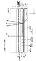
図1に、液晶ディスプレイ装置のパネル断面構造図を示す。この断面構造は、半透過型か透過型かを問わず共通する。また、図1の断面図では、図を見やすくするため断面を表す斜線を省略している。この斜線の省略は、後述する他の断面でも同様である。
図1に図解する液晶ディスプレイ装置10は、映像が表示されユーザが映像を観察する観察面としての表示面11を有する。表示面11は、「表示部」を構成する2枚の基板(後述)に形成された最上層の保護層43の表面(上面)を指す。あるいは、保護層43の表面に更にシートが貼られている場合、そのシートの最表面が表示面11である。
<1. Embodiment>
[Panel structure]
FIG. 1 is a cross-sectional structural view of a liquid crystal display device. This cross-sectional structure is common regardless of whether it is a transflective type or a transmissive type. Further, in the cross-sectional view of FIG. 1, oblique lines representing a cross section are omitted for easy viewing of the drawing. The omission of the oblique lines is the same in other cross sections described later.
A liquid crystal display device 10 illustrated in FIG. 1 has a
「表示部」の表示面11と反対側の最も背面側に、バックライト20が配置されている。
バックライト20は、導光板21、LED等の光源(以下、白色LEDを用いているため「白色光源」と呼ぶ)22、反射ボックス22aを有する。反射ボックス22aで囲まれた白色光源22が、導光板21の少なくとも一方の側面に配置されている。反射ボックス22aは、白色光源22の周囲にLED光が漏れるのを防止して、光の利用効率を上げるための部材である。
特に図示していないが、バックライト20はLED駆動部に接続され、LED駆動部によって白色光源22が発光制御される。また、導光板21の背面側には、反射シートが貼られている。バックライト20は、これらの部材を一体に組み立てた画像ディスプレイ専用の照明装置である。
The
The
Although not particularly illustrated, the
表示部は、2枚のガラス基板として、バックライト20側の駆動基板30と、表示面11側の対向基板31とを有する。
駆動基板30には、細かくなるため詳細には図示していないが、薄膜トランジスタ(TFT)を含む画素内の回路素子や電極が形成され、また、画素のマトリクス駆動のための配線が形成されている。駆動基板30は、スペーサ(不図示)を介して内部空間を形成するように対向基板31と貼り合わされている。このとき、回路素子、電極および配線が形成された駆動基板30の面が、対向基板31と対向している。
The display unit includes a
Although not shown in detail in the
対向基板31には、カラーフィルタ(CF)層34が、基板貼り合わせの前に予め形成されている。
図1の断面構造では対向基板31に、カラーフィルタ層34が示されている。カラーフィルタ層34は、駆動基板30と、対向基板31と、スペーサにより形成される内部空間に面するように対向基板31に予め形成される。
スペーサが形成されていない箇所から、2枚の基板間の内部空間に液晶が注入されている。その後、液晶の注入箇所が閉じられると、液晶が駆動基板30、対向基板31およびスペーサ内に封入され、これにより液晶層35が形成されている。
A color filter (CF)
In the cross-sectional structure of FIG. 1, a
Liquid crystal is injected into the internal space between the two substrates from the portion where the spacer is not formed. Thereafter, when the liquid crystal injection portion is closed, the liquid crystal is sealed in the
図1では細かくなるため図示を省略しているが、このように形成された液晶層35に対し、画素ごとの画素電極と、画素間で共通な共通電極(不図示)とが近接配置される。この2種類の電極は、液晶層35に電圧を印加するための電極である。液晶層35を挟んで2つの電極が配置される場合(縦方向の駆動モード)と、駆動基板30側に2つの電極が2層配置される場合(横方向の駆動モード)とがある。後者の2層配置の場合、両電極は絶縁分離されているが、下層側の共通電極は、上層側で液晶層35に接する画素電極のパターンの間から液晶に電気的な作用を与える。このため、横方向の駆動モードでは電界の向きが横方向となる。これに対し、2つの電極が液晶層35を、その厚さ方向から挟んで配置される場合は、電界の向きが縦方向(厚さ方向)となる。
Although not shown in FIG. 1 because it is fine, a pixel electrode for each pixel and a common electrode (not shown) common to the pixels are arranged close to the
いずれの駆動モード仕様で電極が配置されている場合でも、2つの電極によって液晶層35に対し電圧を印加し、マトリクスに配置された画素を単位として駆動可能である。液晶層35は、その透過を光学的に変調する機能層である。液晶層35は、この印加電圧の大きさに応じて階調表示を行う。
Regardless of the driving mode specification, the electrodes can be driven in units of pixels arranged in a matrix by applying a voltage to the
他の光学機能層として、バックライト20と駆動基板30との間に第1偏光板41が配置されている。また、対向基板31と表示面との間に、第2偏光板42が配置されている。
第2偏光板の表示面11側の面には保護層43が形成されている。
As another optical functional layer, a first
A
本実施形態では、第1偏光板41とバックライト20との間に、検出光出力部50と白色光学フィルム60が配置されている。
検出光出力部50は、物体検出のために表示照明光とは異なる波長領域の光として「検出光」を発光する部品である。ここで、表示照明光が白色LEDの、可視光を主とする波長領域の光である。これに対し、検出光は非可視光、例えば赤外(IR)光である。検出光は可視光でもよいが、可視光だと黒表示のために液晶層35を駆動しているときは遮蔽されるため、表示と検出を同時に行えない場合がある。このため、検出光は非可視光が望ましく、特に赤外光は反射検出に適しているため、更に望ましい。
In the present embodiment, the detection
The detection
検出光出力部50は、導光板51、赤外LED等の光源、反射ボックス53を有する。赤外LED等の光源を、以下、赤外LED52(IR)と呼ぶ。
反射ボックス53で囲まれた赤外LED52(IR)が、導光板51の少なくとも一方の側面に配置されている。反射ボックス53は、赤外LED52(IR)の周囲にLED光が漏れるのを防止して、検出光の利用効率を上げるための部材である。
特に図示していないが、検出光出力部50はLED駆動部に接続され、LED駆動部によって赤外LED52(IR)が発光制御される。また、導光板51の背面側には、反射シートが貼られている。検出光出力部50は、これらの部材を一体に組み立てた反射検出専用の発光装置である。
The detection
An infrared LED 52 (IR) surrounded by the
Although not particularly illustrated, the detection
[赤外光の経路]
つぎに、以上のような構造を有する液晶ディスプレイ装置10のバックライト光および赤外光の経路を説明する。
画像表示時に、バックライト20内で白色光源22が点灯する。すると、白色光源22からの光(表示照明光)が、導光板21の一方端部から導光板21内に入射される。
導光板21は、透明材料からなる反射拡散板の一種であり、LEDといった点光源からの光が導光板21内で反射を繰り返す間に、次第に拡散されて面状の光に変換される。
[Infrared light path]
Next, the paths of backlight light and infrared light of the liquid crystal display device 10 having the above-described structure will be described.
When the image is displayed, the
The
より詳細には、導光板21の上面側(表示面側)の表面では、一部の光が反射されて導光板21の内側に戻され、他の光が導光板21の外部に出てゆく。
導光板21から出た光は、白色光学フィルム60を透過する間に、ある程度拡散した光に変換される。白色光学フィルム60は多層フィルムから形成され、光の拡散機能と、光の光軸を表示面11に対して垂直にする機能を有する。
これに対し、導光板21の背面側の表面では光が漏れないように全反射させる必要がある。背面側に何も設けない場合、一部の光が導光板21から出力しようとする。この出力しようとする光を導光板21に戻すために、背面側に反射シート(不図示)が貼られている。同様な趣旨から、白色光源22の周囲にも反射ボックス22aが設けられている。
バックライト20は、反射シートと反射ボックス22aによって、白色光源22からの光が照明光として効率よく前面側に出射されるようになっている。
More specifically, on the surface on the upper surface side (display surface side) of the
The light emitted from the
On the other hand, it is necessary to totally reflect the light on the back surface of the
The
バックライト20から出射し、白色光学フィルム60を透過した表示照明光は、検出光出力部50を透過する。このとき表示照明光が、光軸の向き変化や光量の減衰をほとんど受けないように白色光学フィルム60が構成されている。
白色光学フィルム60から出射した表示照明光は、表示部で、映像信号に応じた変調を受けて画像光Lとして表示面11から出力される。
The display illumination light emitted from the
The display illumination light emitted from the white
一方、赤外LED52(IR)から出力された赤外光L(IR)は、導光板51内で反射を繰り返して広がり、単位面積あたりの光量が均一化される。赤外LED52(IR)からの出射角度が、導光板51の上面および下面で反射条件を満たす限り、赤外光L(IR)は反射を繰り返して、ほぼ導光板51内に閉じ込められる。特に、下面では反射フィルムで全反射され、また、反射ボックス53等により側面からの漏れも防止される。
On the other hand, the infrared light L (IR) output from the infrared LED 52 (IR) is repeatedly reflected and spreads within the
[構成部材の詳細]
構造等についての詳細は後述するが、導光板51には「光学素子」としてマイクロ(μ)プリズム54が多数配置されている。μプリズム54は、その設けられている場所のほぼ直上の部分のみ赤外光L(IR)を出射させるために設けられている。そのため、μプリズム54の密度や、配置領域と非配置領域の別によって、表示面11から見た赤外光L(IR)の出射領域を任意のパターンとすることが可能である。
μプリズム54からの赤外光L(IR)は、図1に示すように光路が曲げられ、パネル内を通過した後に表示面11から出力される。μプリズム54は、その光路変更面の傾斜角度等によって検出光出力部50の光出射面に対する角度を正確に制御できる。
[Details of components]
Although details of the structure and the like will be described later, the
The infrared light L (IR) from the
表示面11から出力された光が、外部の反射物(被検出物)で反射されると、表示面11を通って再び液晶ディスプレイ装置10内に戻される。被検出物は、人の指やスタイラスペン等の指示手段などである。検出光(本例では赤外光L(IR))が被検出物に反射されることにより戻される光を、以下、反射検出光または反射赤外光Lr(IR)と呼ぶ。
When the light output from the
反射検出光の分布測定のために、複数の受光素子36が表示部内の、例えば駆動基板30に形成されている。
受光素子36は等間隔に配置してもよいが、マイクロレンズと組み合わせて対で配置することが望ましい。
In order to measure the distribution of the reflected detection light, a plurality of light receiving
The
図2は、受光素子とマイクロレンズを組み合わせた場合の拡大断面図である。
駆動基板30の一主面に回路形成層が色ごとに配置されている。回路形成層33(R)と回路形成層33(G)と回路形成層33(B)のそれぞれが映像表示で実効的な画素を形成するサブピクセルに対応している。各回路形成領域は、TFT、キャパシタ電極、配線等の配置領域である。
一方、対向基板31には層間膜38が形成され、層間膜38の液晶層35側に、Rフィルタ34(R),Gフィルタ34(G),Bフィルタ34(B)を含むカラーフィルタ層が形成されている。
FIG. 2 is an enlarged cross-sectional view when a light receiving element and a microlens are combined.
A circuit forming layer is arranged for each color on one main surface of the driving
On the other hand, an
R,G,Bに対応した3つの回路形成領域または3つのフィルタを含む領域を以下、“サブピクセルトリオ”という。一のサブピクセルトリオと、他のサブピクセルトリオとの間の駆動基板30部分が、受光素子の配置領域となっている。受光素子の配置領域は、全体として規則的であれば、例えば、複数のサブピクセルトリオごとに配置してもよい。
ここでは、望ましい配置として、受光素子36_1と36_2が対で配置されている。以下、受光素子36_1と36_2を特に区別する必要がない場合、単に、受光素子36で表記する。
Hereinafter, three circuit formation regions corresponding to R, G, and B or regions including three filters are referred to as “sub-pixel trio”. A portion of the driving
Here, as a desirable arrangement, the light receiving elements 36_1 and 36_2 are arranged in pairs. Hereinafter, when it is not necessary to distinguish between the light receiving elements 36_1 and 36_2, they are simply represented by the
受光素子36は、他のトランジスタと同様にTFT層に形成されるフォトダイオード等である。TFT層はアモルファスシリコンでもポリシリコンでもよい。受光素子36がフォトダイオードの場合、アノードとカソードの2つの高濃度不純物領域の間にI(intrinsic)領域を持つPIN構造、D(doped)領域を持つPDN構造のいずれでもよい。フォトダイオードは、空乏化の程度を制御するコントロールゲートを有していてもよい。
受光素子36_1と36_2からなる受光素子対上に、マイクロレンズ39が形成されている。これにより受光素子対がマイクロレンズ39の集光領域内に配置されている。マイクロレンズ39はサブピクセルトリオの間の領域に配置され、駆動基板30の回路形成面上に堆積された平坦化膜37内に埋め込まれている。
The
A
ここで受光素子対(36_1,36_2)の図2における横(x)方向のピッチは任意であるが、一例を挙げると、例えば0.8[mm]程度である。 Here, the pitch of the light receiving element pair (36_1, 36_2) in the horizontal (x) direction in FIG. 2 is arbitrary, but an example is about 0.8 [mm].
図3(A)は、μプリズム54の形状例を示す斜視図である。図3(B)はμプリズム54による光路変更の様子を示す導光板51の模式断面図である。
図3に図解する本実施の形態のμプリズム54は、断面が三角形状の光学素子であり、導光板51と一体に形成されている。本例のμプリズム54は、例えば導光板51の裏面にV型の溝を形成することで実現できる。なお、μプリズム54を、導光板51とは別のシート等に形成し導光板51に貼り合せるなどの方法でもμプリズム54と同様な機能の光学部品の形成は可能である。
FIG. 3A is a perspective view showing a shape example of the
The
μプリズム54は、赤外LED52(IR)が設けられる導光板51の側面と平行なy方向に長いストライプ形状を有する。そして、当該導光板51の2つのy方向側面間を貫いてμプリズム54が形成されている。
μプリズム54の幅(x方向のサイズ)は、例えば10[μm]程度であり、複数のμプリズム54が、x方向における数十[μm]〜数百[μm]程度の所定ピッチで、y方向に長い平行ストライプ状に配置されている。あるいは十分な光強度を得るため、比較的狭いピッチで数〜数十本のμプリズム54を局所配置し、そのμプリズム54の束を、x方向において比較的大きなピッチで等間隔に配置してもよい。
The
The width (size in the x direction) of the
μプリズム54は、図3(B)に示すように、導光板内側の斜面として、導光板51の2つのx方向側面の一方側に近い第1反射面55aと、他方側に近い第2反射面55bを有する。第1反射面55aと第2反射面55bは、導光板51の背面(反射シート側の全反射面、以下、反出力面という)に対してφ度の傾斜角を有する。この傾斜角はμプリズム54の形成法によって調整される。傾斜角φを45度とすると、反射面に反射した光が最も効率よく検出光として導光板51の出力面(上面)から出てゆく。
As shown in FIG. 3B, the
図3(B)に示すように、傾斜角がφ度の場合、出力面に対する垂線に対し、検出光(赤外光L(IR))は負の角度(−θ)の斜光として出力される。
以上の作用は、他のy方向側面(図3に不図示の左側面)に設けられた赤外LED52(IR)からの光でも同様である。この場合、図3(B)に示す第2反射面55bが実際の反射面となるため、検出光は正の角度(+θ)の斜光として出力される。
この作用は全てのμプリズム54で同じである。このため導光板51の出力面の領域51Bからは、2方向の平行光が検出光として出力される。また、この調整可能な角度(+θ,−θ)は、図1に示す表示面11から検出光が出ていくときもほぼ維持されるため、この角度を検出光の出射角度という。
As shown in FIG. 3B, when the tilt angle is φ degrees, the detection light (infrared light L (IR)) is output as oblique light with a negative angle (−θ) with respect to the perpendicular to the output surface. .
The above operation is the same for the light from the infrared LED 52 (IR) provided on the other side surface in the y direction (the left side surface not shown in FIG. 3). In this case, since the second reflecting
This action is the same for all
この2方向の平行光成分に特化(光束の向きが集約)された検出光は、図1の表示面11から外部へ出射され、外部の被検出物で拡散反射されて表示面11から液晶パネル内に戻される。この反射により戻される光を“反射検出光”という。
ここで検出光の幅がある程度小さく、そのため光が当たっている被検出物の光照射面が小さい場合、その光は被検出物の一点で拡散反射していると推定できる。なぜなら、被検出物は通常、指やスタイラスペン先など、数十〜数百[μm]幅の光より十分大きいからである。
The detection light specialized to the parallel light components in these two directions (the direction of the light beam is aggregated) is emitted from the
Here, when the width of the detection light is small to some extent, and therefore the light irradiation surface of the detection object to which the light hits is small, it can be estimated that the light is diffusely reflected at one point of the detection object. This is because an object to be detected is usually sufficiently larger than light having a width of several tens to several hundreds [μm] such as a finger or a stylus nib.
詳細は後述するが、反射検出光が液晶パネル内を進み、図2に示すマイクロレンズ39に斜めに入る際に、x軸方向の一方からの光は、受光素子対(36_1,36_2)の一方に効率よく集光される。また、他方からの光は受光素子対(36_1,36_2)の他方に効率よく集光される。
ここで、検出光の出射角度(+θ,−θ)は既知の値を有し、この値に応じて、反射検出光の表示面11への入射角度、ひいてはマイクロレンズ39への入射角度も決まる。そのような2つの入射角度を持つ光が効率良く選択的に受光できるように、マイクロレンズ39の屈折率やレンズ面の曲率、さらに、受光素子対(36_1,36_2)の配置等が決められている。よって、受光素子の受光角度は、検出光の出射角度(+θ,−θ)と、マイクロレンズ39の位置、および、受光素子が受光素子対のどちら側の素子であるかに応じて決められる既知の値を有する。ここで選択的な受光は、所定の入射角度の受光感度が他の入射角度より高い感度分布を持つことを含む。
As will be described in detail later, when the reflected detection light travels through the liquid crystal panel and enters the
Here, the emission angles (+ θ, −θ) of the detection light have known values, and the incident angle of the reflected detection light on the
[BL/センサのスキャンと、そのための構成]
後述する3角測量法では、光出射位置と受光位置の対応関係の特定は重要である。
ここで被検出物が、例えば1[mm]程度の小さいものであれば、反射検出光を受光する受光素子対(36_1,36_2)の数も限られるため、その反射検出光の受光位置から逆算すれば、検出光の出射位置も特定できる。しかし、被検出物が比較的大きい場合、その形状が表示面11に平行な平板とは限らないので、その形状が例えば球状の場合、反射検出光分布が広がって受光領域の輪郭がはっきりしない。また、表示面11から出るときの検出光の出射角度(+θ,−θ)と、反射検出光が表示面11に入るときの入射角度が異なるものとなる。このことは、後述する3角測量法では誤差要因となるので、好ましくない。
[BL / sensor scan and configuration for it]
In the triangulation method described later, it is important to specify the correspondence between the light emitting position and the light receiving position.
Here, if the object to be detected is small, for example, about 1 [mm], the number of light receiving element pairs (36_1, 36_2) that receives the reflected detection light is also limited. Therefore, the back calculation is performed from the light receiving position of the reflected detection light. Then, the emission position of the detection light can be specified. However, when the object to be detected is relatively large, the shape is not necessarily a flat plate parallel to the
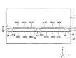
そこで、本実施の形態では、検出光が出射する領域(以下、出射領域という)をストライプ状に限定する。後述するように3角測量の演算負担を減らすには、表示面11に対する出射角度と入射角度の違いが、高さ検出の分解能に応じて3角測量法で許容誤差とみなせる程度まで等価となるように、出射領域の範囲を限定すると望ましい。なお、出射角度と入射角度が等価とみなせない場合は、演算負担が増えるが高さ検出は可能である。具体的な高さ検出手法は後述する。
Therefore, in this embodiment, an area from which the detection light is emitted (hereinafter referred to as an emission area) is limited to a stripe shape. As will be described later, in order to reduce the calculation burden of triangulation, the difference between the emission angle and the incident angle with respect to the
一方で、出射領域をストライプ状に限定すると、検出光が被検出物にヒットしない可能性がある。このため、ストライプ状の検出光の出射領域(以下、輝線BLとよぶ)を、ストライプ幅方向に、所定の距離や画素数のピッチ等でシフトさせる。このとき反射検出光の受光位置も移動する。輝線BLについては後述する図5に示されている。 On the other hand, if the emission region is limited to a stripe shape, the detection light may not hit the object to be detected. For this reason, the emission region of the striped detection light (hereinafter referred to as the bright line BL) is shifted in the stripe width direction by a predetermined distance, a pitch of the number of pixels, or the like. At this time, the light receiving position of the reflected detection light also moves. The bright line BL is shown in FIG.
反射検出光の入射位置の座標(位置情報)を求めるには、輝線BLの位置(またはシフト)ごとに、受光素子の受光結果を外部に出力させるためのスキャン動作を実行する。スキャン動作を行うためには、受光素子を含むセンサ回路にセレクト素子を必要とする。スキャンは、受光素子数が多い場合に配置上の制約で数に限りがある出力線から時系列に出力を取り出すために有効な手法である。 In order to obtain the coordinates (position information) of the incident position of the reflected detection light, a scan operation for outputting the light reception result of the light receiving element to the outside is executed for each position (or shift) of the bright line BL. In order to perform the scanning operation, a select element is required for the sensor circuit including the light receiving element. Scanning is an effective technique for extracting outputs in time series from output lines that are limited in number when there are a large number of light receiving elements.
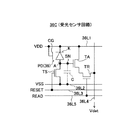
図4に、受光素子36(フォトダイオードPD)を含む受光センサ回路を例示する。
図4に図解する受光センサ回路36Cは、3つのトランジスタ(ここではNチャネル型TFT)とフォトダイオードPD(受光素子36に相当)とを有する。
3つのトランジスタは、リセットトランジスタTS、アンプトランジスタTA、読み出しトランジスタTRである。
FIG. 4 illustrates a light receiving sensor circuit including the light receiving element 36 (photodiode PD).
The light receiving
The three transistors are a reset transistor TS, an amplifier transistor TA, and a read transistor TR.
フォトダイオードPDは、「非可視光に感度を持つ受光素子36(図1および図2参照)」の一例である。フォトダイオードPDは、アノードがストレージノードSNに接続され、カソードが電源電圧VDDの供給線(以下、VDD線)36L1に接続されている。フォトダイオードPDは、PIN構造またはPDN構造を有し、I領域またはD領域に対し絶縁膜を介して電界を及ぼすコントロールゲートCGを備える。フォトダイオードPDは、逆バイアスされて使用され、そのときの空乏化の程度をコントロールゲートCGで制御することにより、感度を最適化(通常、最大化)できる構造を有する。
The photodiode PD is an example of “a
リセットトランジスタTSは、ドレインがストレージノードSNに接続され、ソースが基準電圧VSSの供給線(以下、VSS線)36L2に接続され、ゲートがリセット信号(RESET)の供給線(以下、リセット線)36L3に接続されている。リセットトランジスタTSは、ストレージノードSNをフローティング状態からVSS線36L2への接続状態に切り替え、ストレージノードSNを放電して、その蓄積電荷量をリセットする。 The reset transistor TS has a drain connected to the storage node SN, a source connected to a reference voltage VSS supply line (hereinafter referred to as VSS line) 36L2, and a gate connected to a reset signal (RESET) supply line (hereinafter referred to as reset line) 36L3. It is connected to the. The reset transistor TS switches the storage node SN from the floating state to the connection state to the VSS line 36L2, discharges the storage node SN, and resets the accumulated charge amount.
アンプトランジスタTAは、ドレインがVDD線36L1に接続され、ソースが読み出しトランジスタTRを介して検出電位Vdet(または検出電流Idet)の出力線(以下、検出線)36L4に接続され、ゲートがストレージノードSNに接続されている。
読み出しトランジスタTRは、ドレインがアンプトランジスタTAのソースに接続され、ソースが検出線36L4に接続され、ゲートがリード制御信号(READ)の供給線(以下、リード制御線)36L5に接続されている。
The amplifier transistor TA has a drain connected to the VDD line 36L1, a source connected to the output line (hereinafter referred to as detection line) 36L4 of the detection potential Vdet (or detection current Idet) via the read transistor TR, and a gate connected to the storage node SN. It is connected to the.
The read transistor TR has a drain connected to the source of the amplifier transistor TA, a source connected to the detection line 36L4, and a gate connected to a supply line (hereinafter, read control line) 36L5 of a read control signal (READ).
アンプトランジスタTAは、リセット後に再びフローティング状態となったストレージノードSNにフォトダイオードPDで発生した正電荷が蓄積されると、その蓄積された電荷量(受光電位に相当)を増幅する作用がある。読み出しトランジスタTRは、アンプトランジスタTAで増幅された受光電位を、検出線36L4に排出するタイミングを制御するトランジスタである。一定時間の蓄積時間が経過すると、リード制御信号(READ)が活性化して読み出しトランジスタTRがオンするため、アンプトランジスタTAは、ソースとドレインに電圧が印加されて、そのときのゲート電位に応じた電流を流す。これにより受光電位に応じ、振幅が増大した電位変化が検出線36L4に出現し、この電位変化が、検出電位Vdetとして検出線36L4から受光センサ回路36Cの外部に出力される。あるいは、受光電位に応じて値が変化する検出電流Idetが、検出線36L4から受光センサ回路36Cの外部に出力される。
When the positive charge generated by the photodiode PD is accumulated in the storage node SN that is again in a floating state after reset, the amplifier transistor TA has an effect of amplifying the accumulated charge amount (corresponding to the light receiving potential). The read transistor TR is a transistor that controls the timing at which the light reception potential amplified by the amplifier transistor TA is discharged to the detection line 36L4. When the storage time of a certain time elapses, the read control signal (READ) is activated and the read transistor TR is turned on, so that a voltage is applied to the source and drain of the amplifier transistor TA, and the gate potential at that time Apply current. As a result, a potential change with an increased amplitude appears on the detection line 36L4 in accordance with the light reception potential, and this potential change is output from the detection line 36L4 to the outside of the light
スキャン動作は、リセット線36L3とリード制御線36L5の制御により実行する。これらの配線を、例えば図1〜図3に示す座標系でx方向に並ぶ複数の受光センサ回路36C(受光センサ行)で共通に設けているとする。
この場合、y方向に長い複数の検出線36L4に、受光センサ行の読み出しを行うごとにセンサ読み出し信号(受光信号)が発生する。読み出し行を変えて繰り返し実行される、リセット線36L3とリード制御線36L5の制御ごとに、複数の検出線36L4から受光信号が時系列に表示パネル外部に排出される。
The scan operation is executed by controlling the reset line 36L3 and the read control line 36L5. Assume that these wirings are provided in common in a plurality of light
In this case, a sensor reading signal (light receiving signal) is generated every time the light receiving sensor row is read out on the plurality of detection lines 36L4 that are long in the y direction. For each control of the reset line 36L3 and the read control line 36L5, which is repeatedly executed by changing the readout row, the received light signals are discharged from the plurality of detection lines 36L4 to the outside of the display panel in time series.
つぎに、検出光の出射領域をストライプ状の輝線BLに限定する手段について説明する。
図1に示す構成で液晶層35は映像表示のための光変調層に該当する。映像の非表示時に物体検出を行う場合で、液晶層35が非可視光の透過と遮断を制御できるならば、図1に示す構成も採用可能である。
しかし、物体検出の目的が映像表示時の命令等の情報入力を目的とする場合、検出光をIR光などの非可視光とした上で、液晶層35とは別に、IR光変調手段(例えば液晶層)を設けることが必要となる。
Next, means for limiting the emission region of the detection light to the stripe-like bright lines BL will be described.
In the configuration shown in FIG. 1, the
However, when the object detection purpose is to input information such as a command at the time of displaying an image, the detection light is made invisible light such as IR light, and the IR light modulation means (for example, separate from the liquid crystal layer 35) It is necessary to provide a liquid crystal layer.
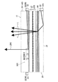
図5は、可視光を変調する液晶層35に加えて、非可視光(IR光)を変調する液晶層35Sを有する場合の構造図である。図5(A)は概略斜視図、図5(B)は概略断面構成図である。
図5は、図1の場合と同様に、バックライト20、白色光学フィルム60および保護層43を有するが、これらを省略し、それ以外の構成を示す概略図である。
図5に図解する液晶ディスプレイ装置は、図1に図解する液晶ディスプレイ装置に比べ、検出光出力部50と駆動基板30との間に、BL走査液晶部LCSが追加されている。
FIG. 5 is a structural diagram in the case of having a
FIG. 5 is a schematic diagram showing a configuration other than the
In the liquid crystal display device illustrated in FIG. 5, a BL scanning liquid crystal unit LCS is added between the detection
図1と同様な構成、すなわち駆動基板30、対向基板31、液晶層35、第1偏光板41および第2偏光板42は、以下、表示液晶部LCと呼ぶ。
なお、図5には、導光板51の反射部材51Rが示されている。
The configuration similar to that shown in FIG. 1, that is, the driving
FIG. 5 shows the reflecting
BL走査液晶部LCSは、表示液晶部LCの駆動基板30、対向基板31に対応した、BL駆動基板30SとBL対向基板31S、ならびに、両基板間のBL液晶層35Sを含む。また、BL走査液晶部LCSは、表示液晶部LCの第1偏光板41と第2偏光板42にそれぞれ対応する、第1偏光板41Sと第2偏光板42Sとを含む。
構造上は表示液晶部LCとBL走査液晶部LCSは似ているが、表示液晶部LCが可視光を変調するのに対し、BL走査液晶部LCSが非可視光(IR光)を変調する。そのため、各部材の材料や光学特性が異なるように表示液晶部LCとBL走査液晶部LCSが構成されている。特に、表示液晶部LCはIR光を常時全面で透過させ、BL走査液晶部LCSは可視光を常時全面で透過させる。
The BL scanning liquid crystal unit LCS includes a
Although the display liquid crystal part LC and the BL scanning liquid crystal part LCS are similar in structure, the display liquid crystal part LC modulates visible light, whereas the BL scanning liquid crystal part LCS modulates invisible light (IR light). Therefore, the display liquid crystal part LC and the BL scanning liquid crystal part LCS are configured so that the materials and optical characteristics of the members are different. In particular, the display liquid crystal unit LC always transmits IR light over the entire surface, and the BL scanning liquid crystal unit LCS transmits visible light over the entire surface.
[高さ検出]
つぎに、高さ検出の手順を説明する。
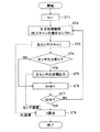
図6は、この手順を示すフローチャートである。このフローチャートのアルゴリズムは、後述する電子機器のCPUやマイクロコンピュータ等の所定の制御部に格納された、あるいは、適宜入力されたプログラムに従って実行される。
[Height detection]
Next, the height detection procedure will be described.
FIG. 6 is a flowchart showing this procedure. The algorithm of this flowchart is executed in accordance with a program stored in a predetermined control unit such as a CPU or a microcomputer of an electronic device described later, or appropriately input.
高さ検出のアルゴリズムが開始すると、ステップST1にて1画面(1フレーム期間)中のBLアドレスNが、例えば“1”に設定される。
つぎのステップST2では、輝線BLの初期制御を行う。つまり、図5に示すBL走査液晶部LCSのBL駆動基板30Sに設けられ、あるいは、一部の機能が表示パネル外の駆動回路に委ねられたBL駆動部が動作する。これにより、N=1の場合の輝線BLを形成する。具体的には、図5(A)に示すように、y方向に長いストライプ状のIR光透過領域としての輝線BLがBL液晶層35Sに形成され、これにより赤外光L(IR)の出射領域の範囲がライン状に絞られる。以下、図1に示す表示面11上での赤外光L(IR)の出射領域を“BL領域”とよぶ。
When the height detection algorithm starts, the BL address N in one screen (one frame period) is set to, for example, “1” in step ST1.
In the next step ST2, initial control of the bright line BL is performed. That is, the
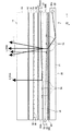
図7に、BL駆動による、BL領域からの赤外光L(IR)の光路変化を装置概略断面により示す。
図7(A)のように、被検出物に赤外光L(IR)が照射されない場合、“反射検出光”としての反射赤外光Lr(IR)は発生しない。
図7(B)のように、被検出物に赤外光L(IR)が当たると、そこで反射赤外光Lr(IR)が発生し、これが液晶ディスプレイ装置に戻される。反射赤外光Lr(IR)は表示液晶部LCの対向基板31と液晶層35を殆ど損失することなく透過し、駆動基板30に設けられた受光素子36(受光センサ回路36C)の配列に到達する。
FIG. 7 is a schematic cross-sectional view of the optical path change of the infrared light L (IR) from the BL region due to BL driving.
As shown in FIG. 7A, when the object to be detected is not irradiated with the infrared light L (IR), the reflected infrared light Lr (IR) as “reflected detection light” is not generated.
As shown in FIG. 7B, when the infrared light L (IR) hits the object to be detected, reflected infrared light Lr (IR) is generated there and returned to the liquid crystal display device. The reflected infrared light Lr (IR) passes through the
図6に戻ると、次のステップST3にて、受光素子36(受光センサ回路36C)の配列に対して、その駆動回路(不図示)が1画面のスキャン動作を行う(光センサスキャン)。駆動回路は通常、液晶ディスプレイ装置10内(駆動基板30内)に形成されるが、その一部が外部に形成されていてもよい。
Returning to FIG. 6, in the next step ST3, the drive circuit (not shown) performs the scanning operation for one screen with respect to the arrangement of the light receiving elements 36 (light receiving
ステップST4ではセンサ出力の有無が判断される。この判断は、液晶ディスプレイ装置の内部、外部のどちらで行ってもよい。通常は、当該液晶ディスプレイ装置10を内蔵する電子機器の制御部が、この判断を行う。
より詳細には、ステップST3の光センサスキャンによって受光信号の1画面の分布が得られるが、その受光信号の分布で、有効なセンサ出力あり、なしを判断する。有効かどうかは、例えば、一定の閾値以上の受光信号レベルがあるかを基準とする。また、ノイズとの区別のため、一定の閾値以上のセンサ出力数が一定の割合以上存在する、あるいは、ある纏まった範囲に存在するといった観点でセンサ出力の有無を判定してもよい。
In step ST4, it is determined whether there is a sensor output. This determination may be made either inside or outside the liquid crystal display device. Normally, the control unit of the electronic device incorporating the liquid crystal display device 10 makes this determination.
More specifically, the distribution of one screen of the received light signal is obtained by the optical sensor scan in step ST3. Based on the distribution of the received light signal, it is determined whether there is an effective sensor output. Whether or not it is valid is based on, for example, whether there is a received light signal level equal to or higher than a certain threshold. Further, in order to distinguish from noise, the presence / absence of sensor output may be determined from the viewpoint that the number of sensor outputs equal to or greater than a certain threshold is greater than a certain ratio or exists in a certain range.
“センサ出力なし(NO)”であれば処理フローがステップST5をスキップし、“センサ出力あり(YES)”であれば、次のステップST5で、出力有りとされた光センサの座標(以下、センサ座標という)を出力する。センサ座標は、高さ(H)算出のため、例えば外部の制御部等の処理ICに出力される。 If “no sensor output (NO)”, the process flow skips step ST5, and if “sensor output exists (YES)”, in the next step ST5, the coordinates of the optical sensor that has been determined to have an output (hereinafter, referred to as “sensor output”). (Referred to as sensor coordinates). The sensor coordinates are output to a processing IC such as an external control unit for calculating the height (H).
ステップST6でBLアドレスNがインクリメントされ(N=N+1)、ステップST7で、BLアドレスNがBL分割数Mに達したかが判断される。
この判断がNOなら、処理フローがステップST2に戻り、ステップST2〜ST7が繰り返される。
ステップST7の判断がYESならば、ステップST8にて、外部の処理IC等で高さ(H)算出処理が実行される。
In step ST6, the BL address N is incremented (N = N + 1), and in step ST7, it is determined whether the BL address N has reached the BL division number M.
If this determination is NO, the process flow returns to step ST2, and steps ST2 to ST7 are repeated.
If the determination in step ST7 is YES, in step ST8, a height (H) calculation process is executed by an external processing IC or the like.
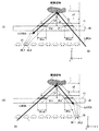
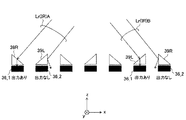
図8(A)は、H算出手法(三角測量法)を模式的に示す説明図である。図8(A)と図8(B)の別は、x軸正側の光源からのIR光(以下、赤外光L(IR)A)の受光時と、x軸負側の光源からのIR光(以下、赤外光L(IR)B)の受光時を示すものである。
図8において、輝線BL(図5参照)に対応して表示面11上のy方向ストライプ領域を、赤外光L(IR)の“出射領域IRout”と定義する。また、被検出物から反射赤外光Lr(IR)が入射される表示面11の領域を“入射領域IRin”と定義する。また、赤外光L(IR)が表示面11と交わる出射角度を“θ1”、反射赤外光Lr(IR)が表示面11と交わる入射角度を“θ2”と定義する。
FIG. 8A is an explanatory diagram schematically showing the H calculation method (triangulation method). 8A and 8B are different from those in the case of receiving IR light (hereinafter, referred to as infrared light L (IR) A) from the x-axis positive light source and from the x-axis negative light source. This shows the time of receiving IR light (hereinafter referred to as infrared light L (IR) B).
In FIG. 8, the y-direction stripe region on the
図8は、赤外光L(IR)と反射赤外光Lr(IR)の範囲と、その代表(例えば中心)線(太線)を示す。IR光の代表線(太線)が表示面11と交差する点をIR光の出射位置と入射位置と定義する。
出射位置のx座標(a1)は、そのときの輝線BLのx座標と、既知の出射角度(+θまたは−θ)と、輝線BLから表示面11までの距離で決まり、予め一意に定まる。
これに対し、入射位置のx座標(a2)は、表示面11から被検出物までの距離(高さH)によって大きく変化する。
入射位置のx座標(a2)は、複数の受光素子36の1画面スキャンにより得られた分布から判定される受光位置中心のx座標を、表示面11上の入射位置のx座標に変換したものである。
FIG. 8 shows the range of the infrared light L (IR) and the reflected infrared light Lr (IR) and the representative (for example, center) line (thick line). The point where the representative line (thick line) of the IR light intersects the
The x coordinate (a1) of the emission position is determined by the x coordinate of the bright line BL at that time, the known emission angle (+ θ or −θ), and the distance from the bright line BL to the
On the other hand, the x coordinate (a2) of the incident position varies greatly depending on the distance (height H) from the
The x coordinate (a2) of the incident position is obtained by converting the x coordinate of the center of the light receiving position determined from the distribution obtained by the one-screen scan of the plurality of light receiving
図6に示すステップST8において、H算出を行う手段(高さ検出部、例えば処理ICや制御部)は、まず、ステップST5で得られたセンサ座標(受光位置中心のx座標)を、表示面11上の入射位置のx座標(a2)に変換し、その実測値を求める。高さ検出部は、ステップST3の処理から出力される輝線BLのx座標(幅中心のx座標)を予め入力して、それから出射位置のx座標(a1)を予め算出し、保持している。 In step ST8 shown in FIG. 6, the means for calculating H (height detection unit, for example, processing IC or control unit) first displays the sensor coordinates (x coordinate of the center of the light receiving position) obtained in step ST5 on the display surface. 11 is converted into the x coordinate (a2) of the incident position on 11 and the actual measurement value is obtained. The height detection unit inputs in advance the x coordinate (x coordinate of the width center) of the bright line BL output from the process of step ST3, and then calculates and holds the x coordinate (a1) of the emission position in advance. .
本発明の実施の形態では、図8(A)または図8(B)の一方で得られた情報から高さHを算出する第1の算出方法と、図8(A)と図8(B)の異なる向きのスキャンで得られた情報から高さHを算出する第2の算出方法のいずれかが採用できる。 In the embodiment of the present invention, the first calculation method for calculating the height H from the information obtained in one of FIGS. 8A and 8B, FIGS. 8A and 8B. Any one of the second calculation methods for calculating the height H from the information obtained by scanning in different directions) can be adopted.
《第1の算出方法》
第1の算出方法の前提として、表示面11に対する出射角度θ1の違い(変動)と入射角度θ2の違い(変動)の各々が、高さ検出の分解能に応じて3角測量法で許容誤差とみなせる程度まで等価となることと要する。この前提が得られる(上記2つの変動の各々が実質的に1つの値と見なせる)ように、出射領域IRoutの範囲が限定されている。つまり、図8(A)または図8(B)に示す出射領域IRoutの幅が十分小さく(この幅に対して被検出物の大きさが十分大きく)、そして出射光が被検出物の表面で拡散反射する場合がこのケースに対応する。被検出物が表示面11と平行な状態でも、この平行な状態から被検出物が傾いても、出射角度θ1と入射角度θ2は変化しない。そのため、出射角度θ1と入射角度θ2の両者は、高さ検出の分解能に応じて3角測量法で許容誤差とみなせる程度まで等価となる。
<< First calculation method >>
As a premise of the first calculation method, each of the difference (variation) in the emission angle θ1 with respect to the
高さHに関する次式(1)、すなわち、
[数1]
H=|a1−a2|*tanθ1*tanθ2/(tanθ1+tanθ2)…(1)
を、図8(A)または図8(B)に示す片方の平行光について立てる。この場合、出射位置のx座標(a1)、入射位置のx座標(a2)、出射角度θ1、入射角度θ2は全て既知である。よって、単に、上記式(1)を1回解くと、高さHが求められる。この場合、測定精度は若干低下するが、入射角度θ2は90度でも高さHを求めることは可能である。
The following expression (1) regarding the height H, that is,
[Equation 1]
H = | a1-a2 | * tan θ1 * tan θ2 / (tan θ1 + tan θ2) (1)
Is set for one parallel light shown in FIG. 8 (A) or FIG. 8 (B). In this case, the x coordinate (a1) of the emission position, the x coordinate (a2) of the incident position, the emission angle θ1, and the incident angle θ2 are all known. Therefore, the height H is obtained simply by solving the above equation (1) once. In this case, although the measurement accuracy slightly decreases, the height H can be obtained even when the incident angle θ2 is 90 degrees.
《第2の算出方法》
出射角度θ1または入射角度θ2が等価とみなせない場合、例えば、図8(A)に示す向きのスキャンにより得られた出射位置のx座標(a1)および入射位置のx座標(a2)と、出射角度θ1(既知)とを、上記式(1)に代入する。ここで、入射角度θ2と高さHが未知のパラメータである。
つぎに、図8(B)に示す向きのスキャンにより得られた出射位置のx座標(a1)および入射位置のx座標(a2)と、出射角度θ1(既知)とを、入射角度θ2と高さHを未知パラメータとする上記式(1)に代入する。
<< Second calculation method >>
When the emission angle θ1 or the incident angle θ2 cannot be regarded as equivalent, for example, the x-coordinate (a1) of the emission position and the x-coordinate (a2) of the incident position obtained by scanning in the direction shown in FIG. The angle θ1 (known) is substituted into the above equation (1). Here, the incident angle θ2 and the height H are unknown parameters.
Next, the x-coordinate (a1) of the emission position and the x-coordinate (a2) of the incident position obtained by the scan in the direction shown in FIG. 8B, the emission angle θ1 (known), the incident angle θ2 and the high Substituting into the above equation (1) where the height H is an unknown parameter.
この2つの連立方程式を解くことにより、入射角度θ2を消去すると、高さHが求まる。 By eliminating these two simultaneous equations and eliminating the incident angle θ2, the height H is obtained.
この方法で、受光信号が検出線36L4(図4)から出力されるが、その受光信号が図8(A)のスキャン時のものか、図8(B)のスキャン時のものかは、受光素子36_1に対応する検出線か、受光素子36_2に対応する検出線かで区別できる。 With this method, a light reception signal is output from the detection line 36L4 (FIG. 4). Whether the light reception signal is at the time of scanning in FIG. 8A or at the time of scanning in FIG. A distinction can be made between a detection line corresponding to the element 36_1 and a detection line corresponding to the light receiving element 36_2.
なお、輝線BLのx方向の幅は、ある想定される高さの範囲(検出可能域)で、どの高さの測定でも、図8(A)のときの受光位置と、図8(B)のときの受光位置が重ならないならば、任意に設定できる。つまり、輝線BLのx方向の幅が余りに大きいと、この2つの受光位置が一部重なり、受光位置の正確な判定が難しくなる。ただし、仮に重なっても、受光信号レベルの強い重なり領域と、その両側の受光信号レベルが弱い領域とから2つの受光位置の推定は可能である。 Note that the width of the bright line BL in the x direction is within a certain assumed height range (detectable region), and the light receiving position in FIG. 8A and the light receiving position in FIG. If the light receiving positions at the time do not overlap, they can be set arbitrarily. That is, if the width of the bright line BL in the x direction is too large, the two light receiving positions partially overlap, making it difficult to accurately determine the light receiving position. However, even if they overlap, it is possible to estimate two light receiving positions from the overlapping region where the light receiving signal level is strong and the region where the light receiving signal level on both sides is weak.
一方、輝線BLのx方向の幅が余りに小さいと、BLスキャンや、そのBLステップ移動ごとのセンサスキャンに多くの時間を要する。
したがって、この2つの観点から妥当な輝線BLのx方向の幅が決められる。
決められた輝線BLのx方向の幅で、出射角度θ1と入射角度θ2が等価とみなせるかどうかに応じて上記第1の算出方法を採用するか、上記第2の算出方法を採用するかを決めればよい。
On the other hand, if the width of the bright line BL in the x direction is too small, a long time is required for the BL scan and the sensor scan for each BL step movement.
Therefore, an appropriate width of the bright line BL in the x direction is determined from these two viewpoints.
Whether to adopt the first calculation method or the second calculation method depending on whether the emission angle θ1 and the incident angle θ2 can be regarded as equivalent with the determined width of the bright line BL in the x direction. Just decide.
また、図2に示すマイクロレンズ39を設けると、光が重なっても、その入射方向によって受光素子36_1が感度を持つか、受光素子36_2が感度を持つかが異なるため、より確実に受光位置の判定が可能となる。また、レンズの集光能力によって検出感度が向上しており、光源の出力を高くしなくても細い輝線BLとすることができる。つまり、マイクロレンズ39と受光素子対とを設けることは、上記第2の算出方法を実行する場合に望ましいが、それに限らず、光が重なる場合でも有用なため、第1の算出方法を実行する場合でも採用可能である。
In addition, when the
また、図8(A)の場合で次式(2−1)、図8(B)の場合で次式(2−2)を用いると、被検出物までの原点からのx方向の距離Lも算出可能である。
[数2]
L=H/tanθ1+a1…(2−1)
L=H/tanθ2+a2…(2−2)
Further, when the following equation (2-1) is used in the case of FIG. 8A and the following equation (2-2) is used in the case of FIG. 8B, the distance L in the x direction from the origin to the detected object. Can also be calculated.
[Equation 2]
L = H / tan θ1 + a1 (2-1)
L = H / tan θ2 + a2 (2-2)
<2.変形例1>
図9に、マイクロレンズと受光素子の変形例を示す。
図9に示すように、マイクロレンズ39を、y軸を長軸とするシリンドリカルレンズにより形成してもよい。その場合、受光素子36_1と受光素子36_2を、シリンドリカルレンズの底面の中心軸(長軸)の左右に互い違いに配置する。各受光素子の受光面の形状を、長軸に沿った帯状とする。
このようにすることにより、画素のy方向と同じサイズのセンサ配置領域を有効に利用して高感度にすることができる。
<2.
FIG. 9 shows a modification of the microlens and the light receiving element.
As shown in FIG. 9, the
By doing so, it is possible to increase the sensitivity by effectively using the sensor arrangement region having the same size as the y direction of the pixel.
図10に、マイクロレンズ配置の変形例を示す。
図10に示すように、マイクロレンズ39は、カラーフィルタ層34と同一面に形成して層間膜38中に埋め込んでもよい。
FIG. 10 shows a modification of the microlens arrangement.
As shown in FIG. 10, the
図8に示すマイクロレンズ39に代えて、図11に示されるように、非対象レンズ対(39R,39L)を、例えばシート状に配置してもよい。
x方向正側に入射面を持つ三角レンズ39Rは、反射赤外光Lr(IR)Aを有効に受光素子36_1に導くが、赤外光L(IR)Bを受光素子に導かない。これとは逆に、x方向負側に入射面を持つ三角レンズ39Lは、反射赤外光Lr(IR)Bを有効に受光素子36_2に導くが、赤外光L(IR)Aを受光素子に導かない。
マイクロレンズ39と同様な機能は、このような光学素子でも実現できる。
Instead of the
The
A function similar to that of the
<3.変形例2>
図12〜図14に、検出光出力部に関する変形を示す。
赤外光L(IR)の光路を表示面11側に変更する光学素子は、実施の形態のようにV溝が形成方法の容易さや加工精度の高さから望ましい。
しかし、反射検出光の検出に支障がないか、反射検出光の邪魔にならない特殊な光学素子が実現できれば、例えば図12と図13に示すように、液晶モジュール(LC+LCS)より表示面11側に配置するとよい。これにより、三角測量法を実施する表示面11と、受光面とが近くなり、その分、距離換算誤差が小さくなるという利点がある。
<3.
12 to 14 show modifications relating to the detection light output unit.
In the optical element that changes the optical path of the infrared light L (IR) to the
However, if a special optical element that does not hinder the detection of the reflection detection light or does not interfere with the reflection detection light can be realized, for example, as shown in FIGS. 12 and 13, the liquid crystal module (LC + LCS) is closer to the
具体的に、図12では、検出光出力部50を、液晶モジュールと保護層43の間に配置している。
図13では、検出光出力部50の機能と保護層43の機能を併せ持つ検出光出力部50Cを配置している。この場合、検出光出力部50Aの表面が表示面11となる。
なお、図14に示すように、x方向正側にIR光源を持つ検出光出力部50Cと、x方向負側にIR光源を持つ検出光出力部50Bとを重ねて配置してもよい。この変形は、図12の変形と重複適用できる。
Specifically, in FIG. 12, the detection
In FIG. 13, a detection
As shown in FIG. 14, a detection
その他、本実施の形態では種々の変形が可能である。
出射領域(BL走査液晶部LCSによる光透過領域)の形状は、ストライプ状に限らない。例えば、「断線平行ストライプ状」「断線千鳥状」などでもよい。その他、規則的なパターンであれば、出射領域の形状や配置は任意である。
In addition, various modifications can be made in the present embodiment.
The shape of the emission region (light transmission region by the BL scanning liquid crystal unit LCS) is not limited to the stripe shape. For example, “disconnected parallel stripes” or “disconnected staggered” may be used. In addition, if it is a regular pattern, the shape and arrangement of the emission region are arbitrary.
以上の実施の形態および変形例は、液晶ディスプレイ装置に本発明の反射検出装置の機能を備えた場合を例として説明したが、この表示装置は他の表示装置、例えば有機EL表示装置であってもよい。
また、本発明が適用された表示装置を内蔵する電子機器は、PC、テレビジョン装置、携帯電話やPDA等の携帯機器、動画または静止画を撮影するカメラ装置、ナビゲーションなどの車載機器など、どのようなものでもよい。
In the above embodiments and modifications, the case where the liquid crystal display device has the function of the reflection detection device of the present invention has been described as an example. However, this display device is another display device, for example, an organic EL display device. Also good.
In addition, electronic devices incorporating a display device to which the present invention is applied include PCs, television devices, mobile devices such as mobile phones and PDAs, camera devices that capture moving images or still images, and in-vehicle devices such as navigation devices. Something like that.
以上より、被検出物の光出射面(表示面)からの距離である高さを容易、かつ正確に測定することができる反射検出装置、および、表示装置が実現できる。
また、反射検出装置または表示装置を搭載した電子機器において、高さ検出を種々のアプリケーションに応用することが容易となる。このため、PC、携帯電話、ゲームなどに全く新しいアプリケーションが創出されることが期待できる。
From the above, it is possible to realize a reflection detection device and a display device that can easily and accurately measure the height, which is the distance from the light emitting surface (display surface) of the object to be detected.
Moreover, it becomes easy to apply height detection to various applications in an electronic apparatus equipped with a reflection detection device or a display device. For this reason, it can be expected that completely new applications will be created in PCs, mobile phones, games and the like.
10等…液晶ディスプレイ装置、11…表示面、30…駆動基板、31…対向基板、35…液晶層、36…受光素子、39…マイクロレンズ、50等…検出光出力部、51…導光板、52(IR)…赤外LED、54…μプリズム。 DESCRIPTION OF SYMBOLS 10 etc .... Liquid crystal display device, 11 ... Display surface, 30 ... Drive board, 31 ... Opposite substrate, 35 ... Liquid crystal layer, 36 ... Light receiving element, 39 ... Micro lens, 50 etc .... Detection light output part, 51 ... Light guide plate, 52 (IR): Infrared LED, 54: μ prism.
Claims (13)
光出射面内の一部の領域である出射領域から斜めに検出光を出射する検出光出力部と、
前記検出光が前記出射領域から外部に出射され、外部で反射されて前記光出射面へ所定角度で入射する反射検出光を選択的に受光し受光信号を出力する複数の受光素子と、
前記反射検出光を受光した受光素子の位置情報と、前記検出光が出射された出射領域の位置情報とを用いて、前記検出光が外部で反射された箇所について、前記光出射面からの距離である高さを求める高さ検出部と、
を有し、
前記検出光出力部は、光出射面内で相反する2つの向きに傾き角成分を持つ2つの平行光を、前記検出光として前記出射領域から出力するとともに、前記相反する2つの向きと平行な方向内で前記出射領域をシフトすることが可能に構成されている、
反射検出装置。 A light exit surface;
A detection light output unit that emits detection light obliquely from an emission region that is a partial region in the light emission surface;
A plurality of light receiving elements that selectively receive reflected detection light that is emitted outside from the emission region, reflected outside, and incident on the light emission surface at a predetermined angle, and outputs a light reception signal;
Using the position information of the light receiving element that has received the reflected detection light and the position information of the emission area from which the detection light is emitted, the distance from the light emission surface for the location where the detection light is reflected externally A height detector for obtaining a height of
I have a,
The detection light output unit outputs two parallel lights having inclination angle components in two opposite directions in the light emission surface as the detection light from the emission region, and is parallel to the two opposite directions. Configured to shift the exit area in a direction ,
Reflection detection device.
前記シフトの方向における前記反射検出光の入射位置の座標a2と、当該座標a2が得られたときにおける前記出射領域の位置の座標a1とを、前記2つの平行光それぞれにおいて求め、
求めた2つの座標a1,a2と、前記検出光の前記光出射面に対する出射角度θ1を用いて、前記反射検出光の前記光出射面への入射角度θ2と前記高さに対応する値Hとを未知数とする次式(1)、すなわち、
H=|a1−a2|*tanθ1*tanθ2/(tanθ1+tanθ2)…(1)
を前記2つの平行光それぞれについて立て、立てた2つの式を解くことにより前記高さに対応する値Hを求める、
請求項1に記載の反射検出装置。 The height detector is
The coordinates a2 of the incident position of the reflected detection light in the shift direction and the coordinates a1 of the position of the emission area when the coordinate a2 is obtained are obtained for each of the two parallel lights.
Using the obtained two coordinates a1 and a2 and an emission angle θ1 of the detection light with respect to the light emission surface, an incident angle θ2 of the reflected detection light to the light emission surface and a value H corresponding to the height The following equation (1) where
H = | a1-a2 | * tan θ1 * tan θ2 / (tan θ1 + tan θ2) (1)
For each of the two parallel lights, and by solving the two equations, a value H corresponding to the height is obtained .
The reflection detection apparatus according to claim 1 .
入力される映像信号に応じて変調された可視光を前記表示面から外部に出力する画像表示の機能と、 表示面内の一部の領域である出射領域から斜めに検出光を出射する機能とを持つ表示部と、
前記検出光が前記出射領域から外部に出射され、外部で反射されて前記表示面へ所定角度で入射する反射検出光を選択的に受光し受光信号を出力する複数の受光素子と、
前記反射検出光を受光した受光素子の位置情報と、前記検出光が出射された出射領域の位置情報とを用いて、前記検出光が外部で反射された箇所について、前記表示面からの距離である高さを求める高さ検出部と、
を有する表示装置。 A display surface;
A function of image display for outputting visible light modulated according to an input video signal to the outside from the display surface, and a function of emitting detection light obliquely from an emission region which is a partial region in the display surface; A display unit having
A plurality of light receiving elements that selectively receive reflected detection light that is emitted outside from the emission region, reflected outside, and incident on the display surface at a predetermined angle, and outputs a light reception signal;
Using the position information of the light receiving element that has received the reflected detection light and the position information of the emission region from which the detection light is emitted, the location where the detection light is reflected externally is a distance from the display surface. A height detector for obtaining a certain height;
A display device.
前記高さ検出部は、
前記シフトの方向における前記反射検出光の入射位置の座標a2と、当該座標a2が得られたときにおける前記出射領域の位置の座標a1とを求め、
前記検出光の前記光出射面に対する出射角度をθ1、前記反射検出光の前記光出射面に対する入射角度をθ2としたとき、求めた2つの座標a1,a2と、前記出射角度θ1および前記入射角度θ2と、を用いて前記高さに対応する値Hを次式(1)、すなわち、
H=|a1−a2|*tanθ1*tanθ2/(tanθ1+tanθ2)…(1)
を解くことにより求める、
請求項3に記載の表示装置。 The display unit is configured to be able to shift the emission region that emits detection light parallel to an oblique direction in one direction,
The height detector is
Obtaining the coordinate a2 of the incident position of the reflected detection light in the shift direction and the coordinate a1 of the position of the emission area when the coordinate a2 is obtained;
When the exit angle of the detection light with respect to the light exit surface is θ1, and the incident angle of the reflected detection light with respect to the light exit surface is θ2, the obtained two coordinates a1, a2, the exit angle θ1, and the entrance angle Using θ2, a value H corresponding to the height is expressed by the following equation (1), that is,
H = | a1-a2 | * tan θ1 * tan θ2 / (tan θ1 + tan θ2) (1)
Determined by solving,
The display device according to claim 3 .
前記高さ検出部は、
前記シフトの方向における前記反射検出光の入射位置の座標a2と、当該座標a2が得られたときにおける前記出射領域の位置の座標a1とを、前記2つの平行光それぞれにおいて求め、
求めた2つの座標a1,a2と、前記検出光の前記表示面に対する出射角度θ1を用いて、前記反射検出光の前記表示面への入射角度θ2と前記高さに対応する値Hとを未知数とする次式(1)、すなわち、
H=|a1−a2|*tanθ1*tanθ2/(tanθ1+tanθ2)…(1)
を前記2つの平行光それぞれについて立て、立てた2つの式を解くことにより前記高さに対応する値Hを求める、
請求項3に記載の表示装置。 The display unit outputs two parallel lights having inclination angle components in two opposite directions on the display surface as the detection light from the emission region, and in a direction parallel to the two opposite directions. It is configured to be able to shift the emission region,
The height detector is
The coordinates a2 of the incident position of the reflected detection light in the shift direction and the coordinates a1 of the position of the emission area when the coordinate a2 is obtained are obtained for each of the two parallel lights.
Using the obtained two coordinates a1 and a2 and the emission angle θ1 of the detection light with respect to the display surface, an incident angle θ2 of the reflected detection light to the display surface and a value H corresponding to the height are unknown. The following equation (1):
H = | a1-a2 | * tan θ1 * tan θ2 / (tan θ1 + tan θ2) (1)
For each of the two parallel lights, and by solving the two equations, a value H corresponding to the height is obtained .
The display device according to claim 3 .
表示光の第1面発光部と、
前記表示面に対し所定の角度で面状の前記検出光を出射する第2面発光部と、
前記第1および第2面発光部と前記表示面との間に配置され、前記第1面発光部からの表示光を入力映像信号に応じて光変調して表示画像光に変換するとともに、前記第2面発光部から出力される前記面状の検出光を、前記表示面の前記出射領域に対応する領域で透過させ、その他の領域で遮断し、透過領域を一方向にシフトする光変調パネル部と、
を有する請求項3に記載の表示装置。 The display unit
A first surface light emitting unit for display light;
A second surface light emitting section for emitting the planar detection light at a predetermined angle with respect to the display surface;
The display light is disposed between the first and second surface light emitting units and the display surface, and the display light from the first surface light emitting unit is optically modulated according to an input video signal and converted into display image light. A light modulation panel that transmits the planar detection light output from the second surface light emitting unit in a region corresponding to the emission region of the display surface, blocks the other region, and shifts the transmission region in one direction. And
The display device according to claim 3 .
前記検出光の光源と、
前記光源からの光を内部反射させて面状光に拡散させる導光板と、
導光板内を通る光の向きを局所的に変更して、前記導光板の表示部側の出力面から斜めに前記面状の検出光を出力させる光学素子と、
を有する請求項6に記載の表示装置。 The second surface light emitter is
A light source of the detection light;
A light guide plate that internally reflects light from the light source and diffuses it into planar light;
An optical element that locally changes the direction of light passing through the light guide plate and outputs the planar detection light obliquely from the output surface on the display unit side of the light guide plate;
The display device according to claim 6 .
前記光学素子が、前記導光板の一方の側面側に配置された第1光源からの光を反射または屈折させる第1光路変更面と、前記導光板の他方の側面側に配置された第2光源からの光を反射または屈折させる第2光路変更面とを有する
請求項3に記載の表示装置。 The light source is disposed on two opposing side surfaces of the light guide plate;
A first optical path changing surface for reflecting or refracting light from a first light source disposed on one side surface of the light guide plate and a second light source disposed on the other side surface of the light guide plate. The display device according to claim 3 , further comprising: a second optical path changing surface that reflects or refracts light from the device.
前記受光素子は、1つの受光レンズに対し対で設けられ、
対で設けられた2つの受光素子が、対応する受光レンズの集光範囲内で一方向に互いに離間して配置されている、
請求項7に記載の表示装置。 Having a plurality of light receiving lenses,
The light receiving elements are provided in pairs for one light receiving lens,
Two light receiving elements provided in pairs are arranged apart from each other in one direction within the light collection range of the corresponding light receiving lens ,
The display device according to claim 7 .
前記表示パネルに表示すべき映像の処理回路を含む回路部と、
を有し、
前記表示パネルは、
前記映像の表示面と、
入力される映像信号に応じて変調された可視光を前記表示面から外部に出力する画像表示の機能と、前記表示面内の一部の領域である出射領域から斜めに検出光を出射する機能とを持つ表示部と、
前記検出光が前記出射領域から外部に出射され、外部で反射されて前記表示面へ所定角度で入射する反射検出光を選択的に受光し受光信号を出力する複数の受光素子と、
を有し、
前記反射検出光を受光した受光素子の位置情報と、前記検出光が出射された出射領域の位置情報とを用いて、前記検出光が外部で反射された箇所について、前記表示面からの距離である高さを求める高さ検出部を有する、
電子機器。 A display panel;
A circuit unit including a video processing circuit to be displayed on the display panel;
Have
The display panel is
A display surface of the video;
A function of image display that outputs visible light modulated according to an input video signal to the outside from the display surface, and a function of emitting detection light obliquely from an emission region that is a partial region in the display surface A display unit with
A plurality of light receiving elements that selectively receive reflected detection light that is emitted outside from the emission region, reflected outside, and incident on the display surface at a predetermined angle, and outputs a light reception signal;
Have
Using the position information of the light receiving element that has received the reflected detection light and the position information of the emission region from which the detection light is emitted, the location where the detection light is reflected externally is a distance from the display surface. Having a height detector for determining a certain height ,
Electronics.
前記高さ検出部は、
前記シフトの方向における前記反射検出光の入射位置の座標a2と、当該座標a2が得られたときにおける前記出射領域の位置の座標a1とを求め、
前記検出光の前記光出射面に対する出射角度をθ1、前記反射検出光の前記光出射面に対する入射角度をθ2としたとき、求めた2つの座標a1,a2と、前記出射角度θ1および前記入射角度θ2と、を用いて前記高さに対応する値Hを次式(1)、すなわち、
H=|a1−a2|*tanθ1*tanθ2/(tanθ1+tanθ2)…(1)
を解くことにより求める、
請求項10に記載の電子機器。 The display unit is configured to be able to shift the emission region that emits detection light parallel to an oblique direction in one direction,
The height detector is
Obtaining the coordinate a2 of the incident position of the reflected detection light in the shift direction and the coordinate a1 of the position of the emission area when the coordinate a2 is obtained;
When the exit angle of the detection light with respect to the light exit surface is θ1, and the incident angle of the reflected detection light with respect to the light exit surface is θ2, the obtained two coordinates a1, a2, the exit angle θ1, and the entrance angle Using θ2, a value H corresponding to the height is expressed by the following equation (1), that is,
H = | a1-a2 | * tan θ1 * tan θ2 / (tan θ1 + tan θ2) (1)
Determined by solving,
The electronic device according to claim 10 .
前記高さ検出部は、
前記シフトの方向における前記反射検出光の入射位置の座標a2と、当該座標a2が得られたときにおける前記出射領域の位置の座標a1とを、前記2つの平行光それぞれにおいて求め、
求めた2つの座標a1,a2と、前記検出光の前記表示面に対する出射角度θ1を用いて、前記反射検出光の前記表示面への入射角度θ2と反射位置の前記高さに対応する値Hとを未知数とする次式(1)、すなわち、
H=|a1−a2|*tanθ1*tanθ2/(tanθ1+tanθ2)…(1)
を前記2つの平行光それぞれについて立て、立てた2つの式を解くことにより前記高さに対応する値Hを求める、
請求項10に記載の電子機器。 The display unit outputs two parallel lights having inclination angle components in two opposite directions on the display surface as the detection light from the emission region, and in a direction parallel to the two opposite directions. The emission area is configured to be shiftable,
The height detector is
The coordinates a2 of the incident position of the reflected detection light in the shift direction and the coordinates a1 of the position of the emission area when the coordinate a2 is obtained are obtained for each of the two parallel lights.
Using the obtained two coordinates a1, a2 and the emission angle θ1 of the detection light with respect to the display surface, a value H corresponding to the incident angle θ2 of the reflected detection light to the display surface and the height of the reflection position. And the following equation (1),
H = | a1-a2 | * tan θ1 * tan θ2 / (tan θ1 + tan θ2) (1)
For each of the two parallel lights, and by solving the two equations, a value H corresponding to the height is obtained .
The electronic device according to claim 10 .
前記検出光が前記出射領域から外部に出射され、外部で反射されて前記表示面へ所定角度で入射する反射検出光を選択的に受光し受光信号を発生する受光のステップと、
前記出射領域を表示面内で一方向にシフトしながら前記光出射のステップを繰り返す走査のステップと、
前記反射検出光を受光した位置情報と、前記検出光が出射された出射領域の位置情報とを用いて、前記検出光が外部で反射された箇所について、前記表示面からの距離である高さを求める高さ検出のステップと、
を含み、
前記光出射のステップでは、表示面内で相反する2つの向きに傾き角成分を持つ2つの平行光を、前記検出光として前記出射領域から出力し、
前記走査のステップでは、前記相反する2つの向きと平行な方向内で前記出射領域をシフトし、
前記高さ検出のステップでは、
前記シフトの方向における前記反射検出光の入射位置の座標a2と、当該座標a2が得られたときにおける前記出射領域の位置の座標a1とを、前記2つの平行光それぞれにおいて求め、
求めた2つの座標a1,a2と、前記検出光の前記表示面に対する出射角度θ1を用いて、前記反射検出光の前記表示面への入射角度θ2と反射位置の前記高さに対応する値Hとを未知数とする次式(1)、すなわち、
H=|a1−a2|*tanθ1*tanθ2/(tanθ1+tanθ2)…(1)
を前記2つの平行光それぞれについて立て、立てた2つの式を解くことにより前記高さに対応する値Hを求める、
反射検出方法。 A light emission step of emitting detection light obliquely from an emission area which is a partial area in the display surface;
A light receiving step of selectively receiving reflected detection light that is emitted from the emission region to the outside, reflected outside and incident on the display surface at a predetermined angle, and generates a light reception signal;
Scanning step for repeating the light emission step while shifting the emission region in one direction within the display surface;
The height, which is the distance from the display surface, at the location where the detection light is reflected outside using the position information where the reflected detection light is received and the position information of the emission region where the detection light is emitted. A height detection step for
Only including,
In the light emission step, two parallel lights having inclination angle components in two opposite directions in the display surface are output from the emission region as the detection light,
In the scanning step, the emission area is shifted in a direction parallel to the two opposite directions,
In the height detection step,
The coordinates a2 of the incident position of the reflected detection light in the shift direction and the coordinates a1 of the position of the emission area when the coordinate a2 is obtained are obtained for each of the two parallel lights.
Using the obtained two coordinates a1, a2 and the emission angle θ1 of the detection light with respect to the display surface, a value H corresponding to the incident angle θ2 of the reflected detection light to the display surface and the height of the reflection position. And the following equation (1),
H = | a1-a2 | * tan θ1 * tan θ2 / (tan θ1 + tan θ2) (1)
For each of the two parallel lights, and by solving the two equations, a value H corresponding to the height is obtained .
Reflection detection method.
Priority Applications (1)
| Application Number | Priority Date | Filing Date | Title |
|---|---|---|---|
| JP2010028845A JP5407918B2 (en) | 2009-02-27 | 2010-02-12 | Reflection detection device, display device, electronic device, and reflection detection method |
Applications Claiming Priority (3)
| Application Number | Priority Date | Filing Date | Title |
|---|---|---|---|
| JP2009045514 | 2009-02-27 | ||
| JP2009045514 | 2009-02-27 | ||
| JP2010028845A JP5407918B2 (en) | 2009-02-27 | 2010-02-12 | Reflection detection device, display device, electronic device, and reflection detection method |
Publications (2)
| Publication Number | Publication Date |
|---|---|
| JP2010225142A JP2010225142A (en) | 2010-10-07 |
| JP5407918B2 true JP5407918B2 (en) | 2014-02-05 |
Family
ID=42654615
Family Applications (1)
| Application Number | Title | Priority Date | Filing Date |
|---|---|---|---|
| JP2010028845A Expired - Fee Related JP5407918B2 (en) | 2009-02-27 | 2010-02-12 | Reflection detection device, display device, electronic device, and reflection detection method |
Country Status (3)
| Country | Link |
|---|---|
| US (1) | US8605057B2 (en) |
| JP (1) | JP5407918B2 (en) |
| CN (1) | CN101819490A (en) |
Families Citing this family (28)
| Publication number | Priority date | Publication date | Assignee | Title |
|---|---|---|---|---|
| US20120068939A1 (en) * | 2010-09-17 | 2012-03-22 | Nigel Patrick Pemberton-Pigott | Touch-sensitive display with depression detection and method |
| US9513737B2 (en) | 2010-09-17 | 2016-12-06 | Blackberry Limited | Touch-sensitive display with optical sensor and method |
| US9223431B2 (en) | 2010-09-17 | 2015-12-29 | Blackberry Limited | Touch-sensitive display with depression detection and method |
| TWI454996B (en) * | 2011-08-18 | 2014-10-01 | Au Optronics Corp | Display and method of determining a position of an object applied to a three-dimensional interactive display |
| TWI526900B (en) * | 2011-12-08 | 2016-03-21 | 原相科技股份有限公司 | Optical touch apparatus, and light source unit and display module for the same |
| KR101181675B1 (en) | 2012-04-09 | 2012-09-24 | 한국기계연구원 | System of cross section inspection using total reflection pattern, method of cross secton inspection thereof, and system of cross section inspection using replica mold, method of cross secton inspection thereof |
| KR101247661B1 (en) * | 2012-04-13 | 2013-04-02 | 한국기계연구원 | Cross section inspection member using total reflection pattern and cross section inspection method thereof |
| KR20140076057A (en) * | 2012-12-12 | 2014-06-20 | 한국전자통신연구원 | Apparatus and method for motion input based on multi-sensor |
| CN103885571B (en) * | 2012-12-19 | 2017-09-29 | 联想(北京)有限公司 | An information processing method and electronic device |
| CN103064085B (en) * | 2012-12-20 | 2015-11-25 | 深圳市华星光电技术有限公司 | Localization method and locating device |
| JP2015022969A (en) * | 2013-07-22 | 2015-02-02 | オムロン株式会社 | Light guide plate transfer molding method, light guide plate, and surface light source device |
| JP2015136061A (en) * | 2014-01-17 | 2015-07-27 | キヤノン株式会社 | Image reading device |
| KR102264379B1 (en) * | 2014-02-05 | 2021-06-15 | 엘지이노텍 주식회사 | Optical device and lighting device using the same |
| CN105718056B (en) * | 2016-01-19 | 2019-09-10 | 北京小米移动软件有限公司 | Gesture identification method and device |
| JP6519505B2 (en) * | 2016-03-15 | 2019-05-29 | オムロン株式会社 | Object detection apparatus, object detection method, and program |
| US10311273B2 (en) * | 2016-10-18 | 2019-06-04 | International Business Machines Corporation | Thermal tags for real-time activity monitoring and methods for detecting the same |
| CN106775137B (en) * | 2016-12-06 | 2019-10-25 | Oppo广东移动通信有限公司 | Proximity detection method and device and mobile terminal |
| CN109671728B (en) * | 2017-10-13 | 2024-05-14 | 深圳芯启航科技有限公司 | Image sensing unit, image sensor and display device |
| KR102540901B1 (en) * | 2018-10-01 | 2023-06-05 | 엘지디스플레이 주식회사 | Display device and display panel with proximity detection sensors |
| CN110058742B (en) * | 2019-04-23 | 2021-01-26 | 京东方科技集团股份有限公司 | Display device, touch detection method and device |
| CN110398748B (en) * | 2019-07-19 | 2022-05-31 | Oppo广东移动通信有限公司 | Distance measuring device, equipment and method |
| CN111339821B (en) * | 2019-12-18 | 2024-12-20 | 深圳阜时科技有限公司 | Optical detection device and electronic equipment |
| JP7654946B2 (en) * | 2020-09-18 | 2025-04-02 | オムロン株式会社 | Non-contact switch |
| CN112634545B (en) * | 2020-11-23 | 2021-10-26 | 中标慧安信息技术股份有限公司 | Infrared scanning management system based on Internet of things |
| CN113031323B (en) * | 2021-03-22 | 2022-09-09 | 绵阳惠科光电科技有限公司 | Frame sealing glue width detection method, display panel and display device |
| CN113076032B (en) * | 2021-05-06 | 2022-12-09 | 深圳市呤云科技有限公司 | Non-touch type elevator car key detection method and key panel |
| CN113785729B (en) * | 2021-09-15 | 2022-09-06 | 湖南怡田美农业科技有限公司 | Rice planting plant diseases and insect pests monitoring devices based on irrigation equipment is last |
| CN115388846B (en) * | 2022-08-25 | 2025-08-01 | 深圳市优必选科技股份有限公司 | Angle determination method, angle determination device, computer equipment and computer readable storage medium |
Family Cites Families (13)
| Publication number | Priority date | Publication date | Assignee | Title |
|---|---|---|---|---|
| JPS62188907A (en) * | 1986-02-14 | 1987-08-18 | Mitsubishi Rayon Co Ltd | Range finder |
| JPH09214751A (en) * | 1996-02-08 | 1997-08-15 | Murata Mach Ltd | Facsimile equipment providing picture reduction function |
| KR100195136B1 (en) * | 1996-10-24 | 1999-06-15 | 윤종용 | Device for measuring height of object |
| JP2000132317A (en) * | 1998-10-21 | 2000-05-12 | Sharp Corp | Area sensor and input device using area sensor |
| CN2613514Y (en) * | 2003-04-09 | 2004-04-28 | 龙历珊珊 | Ultrahigh alarm device |
| US7557935B2 (en) * | 2003-05-19 | 2009-07-07 | Itzhak Baruch | Optical coordinate input device comprising few elements |
| WO2005094306A2 (en) * | 2004-03-29 | 2005-10-13 | Michigan State University | Identification of genes or polypeptides the expression of which correlates to fertility, ovarian function and/or fetal/newborn viability |
| JP4161929B2 (en) * | 2004-04-01 | 2008-10-08 | ソニー株式会社 | Image display device and driving method of image display device |
| JP4515881B2 (en) * | 2004-10-19 | 2010-08-04 | パイオニア株式会社 | Coordinate position detection apparatus and detection method |
| JP4645822B2 (en) * | 2005-04-19 | 2011-03-09 | ソニー株式会社 | Image display device and object detection method |
| US7911444B2 (en) * | 2005-08-31 | 2011-03-22 | Microsoft Corporation | Input method for surface of interactive display |
| US8013845B2 (en) * | 2005-12-30 | 2011-09-06 | Flatfrog Laboratories Ab | Optical touch pad with multilayer waveguide |
| JP2007219676A (en) * | 2006-02-15 | 2007-08-30 | Tokyo Institute Of Technology | Data input device, information device, and data input method |
-
2010
- 2010-02-11 CN CN201010121148A patent/CN101819490A/en active Pending
- 2010-02-12 JP JP2010028845A patent/JP5407918B2/en not_active Expired - Fee Related
- 2010-02-18 US US12/658,978 patent/US8605057B2/en not_active Expired - Fee Related
Also Published As
| Publication number | Publication date |
|---|---|
| CN101819490A (en) | 2010-09-01 |
| US20100220245A1 (en) | 2010-09-02 |
| US8605057B2 (en) | 2013-12-10 |
| JP2010225142A (en) | 2010-10-07 |
Similar Documents
| Publication | Publication Date | Title |
|---|---|---|
| JP5407918B2 (en) | Reflection detection device, display device, electronic device, and reflection detection method | |
| KR101420424B1 (en) | Liquid crystal display device having multi-touch detection function and driving method thereof | |
| JP5528739B2 (en) | Detection device, display device, and method for measuring proximity distance of object | |
| JP5563250B2 (en) | Stereoscopic image display device | |
| CN106773273B (en) | Display device and driving method of display device | |
| CN102200855B (en) | Object-sensing device | |
| JP4553002B2 (en) | Display device | |
| US8780087B2 (en) | Optical touch screen | |
| TW200523788A (en) | Coordinate detection system for a display monitor | |
| US9304627B2 (en) | Display device and display control system | |
| KR20080028208A (en) | Liquid crystal display with multi-touch sensing function and its driving method | |
| US20100225616A1 (en) | Display device with position detecting function and electronic apparatus | |
| US20110261300A1 (en) | Area sensor and display device having area sensor | |
| CN109376616A (en) | Fingerprint identification device, fingerprint identification method and display device thereof | |
| US20250044611A1 (en) | Air floating video information display system | |
| US11733572B2 (en) | Image capturing apparatus | |
| KR20120073269A (en) | Touch screen display device | |
| JP5813533B2 (en) | Input device and input system | |
| JP2010039942A (en) | Reflection detection device, display, electronic equipment, and reflection detecting method | |
| JP2023041339A (en) | Space floating video information display system and stereo sensing device used therefor | |
| JP2023117741A (en) | Spatial floating image information display system and optical system used therefor | |
| JP2023087963A (en) | Spatial floating image information display system and optical system used therefor | |
| WO2012018090A1 (en) | Area sensor and display device | |
| WO2012018092A1 (en) | Area sensor and display device |
Legal Events
| Date | Code | Title | Description |
|---|---|---|---|
| A621 | Written request for application examination |
Free format text: JAPANESE INTERMEDIATE CODE: A621 Effective date: 20130122 |
|
| A977 | Report on retrieval |
Free format text: JAPANESE INTERMEDIATE CODE: A971007 Effective date: 20130717 |
|
| A131 | Notification of reasons for refusal |
Free format text: JAPANESE INTERMEDIATE CODE: A131 Effective date: 20130723 |
|
| A521 | Written amendment |
Free format text: JAPANESE INTERMEDIATE CODE: A523 Effective date: 20130917 |
|
| A01 | Written decision to grant a patent or to grant a registration (utility model) |
Free format text: JAPANESE INTERMEDIATE CODE: A01 Effective date: 20131008 |
|
| A61 | First payment of annual fees (during grant procedure) |
Free format text: JAPANESE INTERMEDIATE CODE: A61 Effective date: 20131021 |
|
| LAPS | Cancellation because of no payment of annual fees |