JP5385500B2 - Signal processing device - Google Patents
Signal processing device Download PDFInfo
- Publication number
- JP5385500B2 JP5385500B2 JP2006080795A JP2006080795A JP5385500B2 JP 5385500 B2 JP5385500 B2 JP 5385500B2 JP 2006080795 A JP2006080795 A JP 2006080795A JP 2006080795 A JP2006080795 A JP 2006080795A JP 5385500 B2 JP5385500 B2 JP 5385500B2
- Authority
- JP
- Japan
- Prior art keywords
- power supply
- supply voltage
- signal processing
- level
- processing apparatus
- Prior art date
- Legal status (The legal status is an assumption and is not a legal conclusion. Google has not performed a legal analysis and makes no representation as to the accuracy of the status listed.)
- Active
Links
Images


Classifications
-
- G—PHYSICS
- G06—COMPUTING; CALCULATING OR COUNTING
- G06F—ELECTRIC DIGITAL DATA PROCESSING
- G06F1/00—Details not covered by groups G06F3/00 - G06F13/00 and G06F21/00
- G06F1/26—Power supply means, e.g. regulation thereof
- G06F1/32—Means for saving power
-
- G—PHYSICS
- G06—COMPUTING; CALCULATING OR COUNTING
- G06F—ELECTRIC DIGITAL DATA PROCESSING
- G06F1/00—Details not covered by groups G06F3/00 - G06F13/00 and G06F21/00
- G06F1/26—Power supply means, e.g. regulation thereof
- G06F1/263—Arrangements for using multiple switchable power supplies, e.g. battery and AC
-
- G—PHYSICS
- G06—COMPUTING; CALCULATING OR COUNTING
- G06F—ELECTRIC DIGITAL DATA PROCESSING
- G06F1/00—Details not covered by groups G06F3/00 - G06F13/00 and G06F21/00
- G06F1/26—Power supply means, e.g. regulation thereof
-
- G—PHYSICS
- G06—COMPUTING; CALCULATING OR COUNTING
- G06F—ELECTRIC DIGITAL DATA PROCESSING
- G06F1/00—Details not covered by groups G06F3/00 - G06F13/00 and G06F21/00
- G06F1/26—Power supply means, e.g. regulation thereof
- G06F1/30—Means for acting in the event of power-supply failure or interruption, e.g. power-supply fluctuations
Landscapes
- Engineering & Computer Science (AREA)
- Theoretical Computer Science (AREA)
- Physics & Mathematics (AREA)
- General Engineering & Computer Science (AREA)
- General Physics & Mathematics (AREA)
- Power Engineering (AREA)
- Power Sources (AREA)
Description
本発明は、信号処理装置に関する。 The present invention relates to a signal processing apparatus.
近年のエレクトロニクス技術の伸展に伴って、携帯オーディオ再生機器、携帯電話、携帯型ゲーム、PDA(Personal Digital Assistants)等といった、持ち運び便利な携帯性を売りとし且つ所望のアプリケーションに係る信号処理を実行する信号処理装置の普及がめざましい。かかる信号処理装置は、二次電池(ニッケル水素充電池、リチウムイオン充電池等)や一次電池(アルカリ乾電池、マンガン乾電池等)によって構成された内部電源を搭載することで携帯性を実現している(例えば、以下に示す特許文献1を参照)。
ところで、内部電源の電源電圧のみで所望のアプリケーションを長時間実行すると、当然の結果として内部電源の電力消費は増大する。従って、信号処理装置は、多種多様なアプリケーションを長時間実行させる意味で、さらなる低消費電力化の対策が必須となっており、既存の対策では不十分であった。 By the way, if a desired application is executed for a long time using only the power supply voltage of the internal power supply, the power consumption of the internal power supply naturally increases. Therefore, in the signal processing apparatus, a measure for further reducing power consumption is indispensable in order to execute a wide variety of applications for a long time, and existing measures are insufficient.
前述した課題を解決するための主たる本発明は、レギュレート回路が電源電圧のレベルを調整して第1の電源電圧を生成するように、前記レギュレート回路に前記電源電圧を供給する外部電源、又は、前記第1の電源電圧よりもレベルの低い第2の電源電圧を供給する内部電源、のうちいずれかが印加されて動作する信号処理装置において、前記外部電源から供給される前記電源電圧のレベルを調整して前記第1の電源電圧を前記レギュレート回路で生成する前の前記電源電圧のレベルを監視して、前記外部電源から、前記第1の電源電圧を前記レギュレート回路で生成する前の前記電源電圧が供給されているか否かを判定し、前記第1の電源電圧を前記レギュレート回路で生成する前の前記電源電圧が供給されている旨が判定された場合には前記第1の電源電圧が印加され、前記第1の電源電圧を前記レギュレート回路で生成する前の前記電源電圧が供給されていない旨が判定された場合には前記第2の電源電圧が印加されるように制御する電源電圧監視部、を備え、前記電源電圧監視部は、前記第1の電源電圧を前記レギュレート回路で生成する前の前記電源電圧が印加される端子の電圧レベルを予め定めておいた参照レベルと比較して、Highレベル若しくはLowレベルの二値化信号を出力する二値化処理部と、前記二値化信号のHighレベル若しくはLowレベルの期間が一定期間継続したときに、前記二値化信号に応じて、前記レギュレート回路によって生成されている前記第1の電源電圧又は前記第2の電源電圧を選択するための選択信号を生成する判定処理部と、を備え、前記外部電源は、データ通信を行うとともに前記第1の電源電圧を供給可能なインタフェースより供給され、前記第1の電源電圧を前記レギュレート回路で生成する前の前記電源電圧は、前記外部電源を前記インタフェースに供給するためのケーブルが前記インタフェースに接続された場合、時間が経過するにつれて徐々に上昇し、前記ケーブルが前記インタフェースから取り外された場合、時間が経過するにつれて徐々に減衰し、前記ケーブルが前記インタフェースに接続される場合、前記第1の電源電圧は、前記ケーブルが前記インタフェースに接続された時から、前記端子の電圧レベルが前記参照レベルを上回った後、更に前記一定期間が経過するまでの間に、生成されており、前記ケーブルが前記インタフェースから取り外される場合、前記第1の電源電圧は、前記ケーブルが前記インタフェースから取り外された時から、前記端子の電圧レベルが前記参照レベルを下回った後、更に前記一定期間が経過するまでの間、供給され続けている。 The main aspect of the present invention for solving the above-described problem is an external power supply that supplies the power supply voltage to the regulator circuit so that the regulator circuit adjusts the level of the power supply voltage to generate the first power supply voltage. Alternatively, in a signal processing device that operates by applying any one of an internal power supply that supplies a second power supply voltage that is lower in level than the first power supply voltage, the power supply voltage supplied from the external power supply The level of the power supply voltage is monitored before the first power supply voltage is generated by the regulation circuit by adjusting the level, and the first power supply voltage is generated by the regulation circuit from the external power supply. When it is determined whether or not the previous power supply voltage is supplied, and it is determined that the power supply voltage before the first power supply voltage is generated by the regulation circuit is supplied When the first power supply voltage is applied and it is determined that the power supply voltage before the first power supply voltage is generated by the regulation circuit is not supplied, the second power supply voltage is applied. A power supply voltage monitoring unit that controls the power supply voltage monitoring unit to control a voltage level of a terminal to which the power supply voltage is applied before the first power supply voltage is generated by the regulation circuit. Compared with a predetermined reference level, when a binarization processing unit that outputs a binarized signal of high level or low level and a period of high level or low level of the binarized signal continues for a certain period And a determination processing unit that generates a selection signal for selecting the first power supply voltage or the second power supply voltage generated by the regulation circuit according to the binarization signal. , Wherein the external power source is supplied from capable of supplying interfacing the first power supply voltage and performs data communication, the power supply voltage before generating the first power supply voltage by the regulator circuit, When a cable for supplying the external power to the interface is connected to the interface, it gradually rises as time passes, and when the cable is removed from the interface, it gradually decays as time passes and, when the cable is connected to the interface, the first power supply voltage, since the pre-listen Buru is connected to the interface, after the voltage level of the terminal exceeds the reference level, further Generated until the predetermined period of time elapses, and the cable is disconnected from the interface. If removed, the first power supply voltage is between when the cable is disconnected from the interface and after the voltage level of the terminal falls below the reference level until the fixed period elapses. It continues to be supplied .
本発明によれば、外部電源の供給状態に応じて供給する電源電圧を適切に制御することにより、集積回路における電力消費を低減することができる。 According to the present invention, it is possible to reduce power consumption in an integrated circuit by appropriately controlling a power supply voltage to be supplied according to a supply state of an external power supply.
<信号処理装置の外部接続>
図1は、本発明に係る信号処理装置の外部接続を説明するための図である。以下では、本発明に係る信号処理装置の一例として、USB(Universal Serial Bus)インタフェース101を備えており、パーソナルコンピュータ300からUSBケーブル400のデータライン401を介して転送された圧縮オーディオデータのデジタル再生を行う携帯オーディオ再生機器100を採りあげて説明する。なお、本発明に係る信号処理装置は、例えば、携帯電話、携帯型ゲーム、PDA等であってもよい。
<External connection of signal processor>
FIG. 1 is a diagram for explaining external connections of a signal processing apparatus according to the present invention. Hereinafter, as an example of the signal processing apparatus according to the present invention, a USB (Universal Serial Bus)
ここで、USBとは、共通のUSBインタフェースで様々なタイプの信号処理装置をUSBホスト機器へと接続可能なシリアルインタフェース規格のことである。USBの現時点での最新バージョンは「USB2.0」であり、LS(Low Speed)、FS(Full Speed)及びHS(High Speed)の3種類の転送モードを備えており、用途に応じて3種類の転送モードが使い分けられる。また、USBは、ハブを利用することで最大127個のUSB機器をツリー状に接続可能であり、また、USBホスト機器の電源を投入した状態で新たなUSB機器を接続可能な所謂ホットプラグに対応している。 Here, USB is a serial interface standard that allows various types of signal processing devices to be connected to a USB host device through a common USB interface. The latest version of USB at the moment is “USB2.0”, which has three types of transfer modes: LS (Low Speed), FS (Full Speed), and HS (High Speed). Different transfer modes are used. In addition, USB can connect up to 127 USB devices in a tree shape by using a hub, and is a so-called hot plug that can connect a new USB device with the USB host device powered on. It corresponds.
まず、パーソナルコンピュータ300は、USBコントローラ310並びに2ポートのUSBインタフェース320a、320bを備えてある場合とする。この場合、パーソナルコンピュータ300における2ポートのUSBインタフェース320a、320bのうちいずれか一方と、携帯オーディオ再生機器100におけるUSBインタフェース101との間を、USBケーブル400によって接続することで、パーソナルコンピュータ300と携帯オーディオ再生機器100間がUSB接続される。なお、USBケーブル400は、2本のデータライン401と、電源ライン402と、GNDライン403とによって構成されており、USBインタフェース320a、101は、それぞれ、一対のデータ端子D+及びD−と、電源端子VBUSと、GND端子とが設けられる。
First, it is assumed that the
パーソナルコンピュータ300は、電源プラグ361を差し込んだ商用電源700から供給されるAC電源電圧をDC電源電圧へと変換する電源アダプタ360を備えるとともに、全体の制御を司るCPU330、様々なプログラムを格納するROM等のメモリ340、音楽ファイルや動画ファイル等を格納するハードディスク350、が相互に通信可能に接続されている。ここで、ハードディスク350に格納される音楽ファイルは、例えば、MPEG−1 Audio Layer3(MP3)形式等の圧縮オーディオデータであり、ハードディスク350に格納される動画ファイルは、例えば、MPEG−2形式、MPEG−4形式等の圧縮ムービーデータである。
The
ここで、パーソナルコンピュータ300から携帯オーディオ再生機器100に向けての音楽ファイルのデータ転送の概要を説明する。まず、パーソナルコンピュータ300は、メモリ340に格納されたプログラムを起動し、ポーリング要求等によって携帯オーディオ再生機器100を自身に接続されたUSB機器として認識する。そして、パーソナルコンピュータ300は、ハードディスク350から任意の音楽ファイルを読み出し、USBコントローラ310へとデータ転送する。USBコントローラ310は、ハードディスク350から読み出された音楽ファイルをパケット形式へと変換して、USBインタフェース320a乃至USBケーブル400を介して携帯オーディオ再生機器100へと差動の半二重伝送を行うためのUSB規格に準拠した通信プロトコル処理を行う。この結果、携帯オーディオ再生機器100は、パーソナルコンピュータ300から音楽ファイルを取り込むことができる。
Here, an outline of music file data transfer from the
一方、携帯オーディオ再生機器100は、パーソナルコンピュータ300から音楽ファイルのデータ転送が完了した場合、一般的には、USBインタフェース101からUSBケーブル400を取り外した上で、当該音楽ファイルの再生処理を実行することになる。
On the other hand, when the music file data transfer from the
<信号処理装置が使用可能な外部電源>
前述したUSBのインタフェース101を備えた携帯オーディオ再生機器100は、パーソナルコンピュータ300からUSBケーブル400を介してUSBインタフェース101へと外部電源供給される場合(以下、ケースA)、パーソナルコンピュータ300からUSB補助ケーブル420を介して電源入力端子107へと外部電源供給される場合(以下、ケースB)、若しくは、通常の電源アダプタ600から電源ケーブル610を介して電源入力端子107へと外部電源供給される場合(以下、ケースC)がある。
そこで、以下では、前述したケースA乃至ケースCについてそれぞれ説明する。
<External power supply that can use the signal processing device>
When the portable
Therefore, the cases A to C described above will be described below.
===ケースAについて===
パーソナルコンピュータ300は、USBケーブル400が備える電源ライン402を利用して、携帯オーディオ再生機器100に向けて電源アダプタ360において生成したDC電源電圧(以下、電源電圧VBUSという。)を供給することができる。換言すると、携帯オーディオ再生機器100は、パーソナルコンピュータ300から音楽ファイルの取り込みと併せて電源電圧VBUSの供給を受けることができる。
=== About Case A ===
The
従って、携帯オーディオ再生機器100は、内部電源104の電力消費を抑えるべく、パーソナルコンピュータ300から供給された電源電圧VBUSを動作電圧として、パーソナルコンピュータ300との間のUSB規格に準拠した通信プロトコル処理や音楽ファイルの再生処理を行える。
Therefore, the portable
===ケースBについて===
USBインタフェース320bにUSB電源補助ケーブル420の一端を接続するとともに、USB電源補助ケーブル420の他端を電源入力端子107へと接続することで、パーソナルコンピュータ300の電源電圧VBUSのみを携帯オーディオ機器100に供給することができる。この結果、携帯オーディオ再生機器100は、データ通信を行わずに、USBインタフェース320bより電源電圧VBUSが供給される。
=== About Case B ===
By connecting one end of the USB power supply
===ケースCについて===
携帯オーディオ再生機器100は、電源プラグ601を商用電源700のコンセントに差し込んだ通常の電源アダプタ600から、電源ケーブル610を介して外部電源供給を受けることもできる。パーソナルコンピュータ300と接続せずに内部電源104を充電する場合が考えられる。
=== About Case C ===
The portable
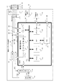
<携帯オーディオ再生機器の構成>
図2は、携帯オーディオ再生機器100の構成を示す図である。同図に示すように、携帯オーディオ再生機器100は、本発明に係る『集積回路』の一実施形態であるASIC(Application Specific Integrated Circuit)200と、その周辺回路によって構成される。なお、本実施形態では、『集積回路』をASIC200によって実現するが、その他にFPGA(Field Programmable Gate Array)やPLD(Programmable Logic Device)で実現してもよい。
<Configuration of portable audio player>
FIG. 2 is a diagram illustrating the configuration of the portable
以下では、携帯オーディオ再生機器100の構成の説明に際して、ASIC200の周辺回路の構成と、ASIC200の構成と、に分けてそれぞれ説明する。
Hereinafter, when the configuration of the portable
===ASIC周辺回路の構成===
USBインタフェース101は、電源ライン402を含んだUSBケーブル400を介してパーソナルコンピュータ300と通信可能に接続させるためのインタフェースである。すなわち、USBインタフェース101は、USBケーブル400の構成と対応づけて、一対のデータ端子D+及びD−と、電源端子VBUSと、GND端子とが設けられる。
=== Configuration of ASIC Peripheral Circuit ===
The
レギュレート回路103は、USBインタフェース101から配線された電源ライン102の電源電圧VBUSのレベルを、高速性が要求される通信プロトコル処理(HSモードやFSモード等)をASIC200が行う場合に必要な動作電圧(3.3Vや1.5V等)へと調整したレギュレート電源電圧VREG(本発明に係る『第1の電源電圧』)を生成する。
The
なお、USBバスパワーとしてパーソナルコンピュータ300から供給され得る電源電圧は「+4.75V〜+5.25V」の範囲と規定されており、本実施形態では、電源電圧VBUSのレベルは「5V」とする。また、レギュレート電源電圧VREGのレベルは「1.5V」とする。
Note that the power supply voltage that can be supplied from the
内部電源104は、一又は複数の二次電池(ニッケル水素充電池(公称電圧1.2V)、リチウムイオン充電池(公称電圧3.6V〜3.7V)等)若しくは一又は複数の一次電池(アルカリ乾電池(公称電圧1.5V)、マンガン乾電池(公称電圧1.5V)等)によって構成される電源であり、レギュレート電源電圧VREGのレベルよりも低いレベルの電源電圧VDD(本発明に係る『第2の電源電圧』)を生成する。なお、内部電源104は、二次電池によって構成する場合には、USBインタフェース101に接続したUSB電源、若しくは、電源入力端子107に接続した電源アダプタ600によって充電される。
The
ここで、本実施形態では、内部電源104は、充電が可能であり且つ公称電圧が最も低い二次電池であるニッケル水素充電池(公称電圧1.2V)によって構成される場合とする。また、電源電圧VDDは、ASIC200の低消費電力化のためにできる限り低いレベルにすることが好ましいが、ASIC200の正常動作が可能な範囲並びにASIC200の半導体プロセスの兼ね合いによって、公称電圧(1.2V)の90%程度の「1.1V」とする。
Here, in the present embodiment, it is assumed that the
電源電圧選択部105は、後述の電源電圧監視部270からDET端子207を介して供給された選択信号DETに基づいて、パーソナルコンピュータ300から携帯オーディオ再生機器100へ向けて電源電圧VBUSが供給されている旨が判定された場合には、レギュレート電源電圧VREGの方を選択する。また、電源電圧選択部105は、前述した選択信号DETに基づいて、パーソナルコンピュータ300から携帯オーディオ再生機器100へ向けて電源電圧VBUSが供給されていない旨が判定された場合には電源電圧VDDの方を選択する。
The power supply
不揮発性メモリ106は、パーソナルコンピュータ300からUSBケーブル400を介して転送された音楽ファイルを格納する外部メモリである。不揮発性メモリ106は、例えば、フラッシュメモリを採用する。なお、本実施形態以外にも、より大容量のデータを格納する場合には、不揮発性メモリ106の代わりに、小型ハードディスク(不図示)を採用してもよい。
The
===ASICの構成===
まず、ASIC200の端子としては、D+端子201、D−端子202、MI端子203、OUT端子204、VBUS端子206、DET端子207、VDD端子208が設けられる。
=== Configuration of ASIC ===
First, as the terminals of the
D+端子201、D−端子202は、USBインタフェース101のデータ端子D+、D−とそれぞれ接続させる入出力端子である。MI端子203は、不揮発性メモリ106と接続させる入出力端子である。OUT端子204は、音楽ファイルの再生結果を出力するための出力端子である。
D + terminal 201, D-
VBUS端子206は、USBインタフェース101の電源端子より配線された電源ライン102と接続させる入力端子である。DET端子207は、電源電圧監視部270の判定結果である選択信号DETを出力する出力端子である。VDD端子208は、電源電圧選択部105において選択されたレギュレート電源電圧VREG若しくは電源電圧VDDの一方が印加される入力端子である。
The
また、ASIC200は、マイクロコンピュータ210、USBコントローラ220、メモリインタフェース回路230、DSP(Digital Signal Processor)240、RAM250、DA変換器260それぞれが内部バス209を介して相互に通信可能に接続されており、更に、電源電圧監視部270を備える。
In the
マイクロコンピュータ210は、ASIC200全体の制御を司るプロセッサである。すなわち、マイクロコンピュータ210は、USBコントローラ220における通信プロトコル処理や、DSP240における音楽ファイルの再生処理等を統括制御する。
The
USBコントローラ220は、パーソナルコンピュータ300との間の通信プロトコル処理を行うものであり、USBインタフェース101からD+端子201並びにD−端子202へと差動入力されてきたデータをASIC200の内部バス209へと中継を行うUSBトランシーバや、パケットをデコードするデコーダ、更にはバッファ用のFIFO等を備える。例えば、USBコントローラ220は、マイクロコンピュータ210からの指令によって、パーソナルコンピュータ300からデータ転送された音楽ファイルを内部バス209を介してメモリインタフェース回路230へと転送する。
The
メモリインタフェース回路230は、ASIC200からMI端子203に接続された不揮発性メモリ106に対するデータの読み出し・書き込みを制御するための回路である。例えば、メモリインタフェース回路230は、USBコントローラ220から転送された音楽ファイルを不揮発性メモリ106へと書き込む処理を行う。
The
DSP240は、音楽ファイルの再生に係るデジタル信号処理を行う回路である。例えば、音楽ファイルの再生の際には、マイクロコンピュータ210からの指令によって、不揮発性メモリ106に書き込まれた音楽ファイルがメモリインタフェース回路230によって読み出され、作業用メモリとしてのRAM250へと格納される。DSP240は、RAM250へと格納された音楽ファイルを読み出してそのデータ形式に準拠したデコード処理(例えば、MP3デコード等)を行う。そして、デコード処理されたデジタル信号が、DA変換器260によってアナログ信号へと変換された後にOUT端子204を介して外部へと出力される。
The
電源電圧監視部270は、USBインタフェース101にUSBケーブル400が接続された場合にパーソナルコンピュータ300から電源ライン402を介して供給され得る電源電圧VBUSのレベルを監視することで、パーソナルコンピュータ300から電源電圧VBUSが供給されているか否かを判定する。
The power supply
詳述すると、電源ライン402とUSBインタフェース101を介して電気的に接続された電源ライン102上にプルダウン抵抗Rdを予め設けておく。その上で、USBインタフェース101にUSBケーブル400が接続されてパーソナルコンピュータ300から電源電圧VBUSの供給を受けている場合にはVBUS端子206に印加される電圧レベルは「5V」となる。一方、USBインタフェース101からUSBケーブル400が取り外された場合にはパーソナルコンピュータ300から電源電圧VBUSの供給を受けられないので、VBUS端子206に印加される電圧レベルはプルダウン抵抗Rdによって「0V」となる。
More specifically, a pull-down resistor Rd is provided in advance on the
そこで、電源電圧監視部270は、二値化処理部271並びに判定処理部272を具備しており、二値化処理部271は、VBUS端子に印加される電圧レベルを予め定めておいた参照レベルVth(例えば、2.5V)と比較することで、Highレベル若しくはLowレベルを出力する。
Therefore, the power supply
判定処理部272は、二値化処理部271より出力されたHighレベル又はLowレベルの期間を計測することで、Highレベルが一定期間Th継続した場合にはパーソナルコンピュータ300から電源電圧VBUSが供給されている旨を判定し、Lowレベルが一定期間Th継続した場合にはパーソナルコンピュータ300から電源電圧VBUSが供給されていない旨を判定する。このように、二値化処理部271より出力されるHighレベル又はLowレベルが一定期間Th継続するまでは判定を下さないことで、例えば、スパイク状の電源ノイズの影響を受けて、誤った判定結果が引き起こされることを防止できる。
The
なお、判定処理部272における判定結果は、電源電圧選択部105がレギュレート電源電圧VREG又は電源電圧VDDを選択するための選択信号DETとして用いられる。ここで、電源電圧選択部105は、ASIC200の周辺回路であるため、選択信号DETは、DET端子207を介して電源電圧選択部105へと出力される。
The determination result in the
すなわち、パーソナルコンピュータ300から携帯オーディオ再生機器100に向けて電源電圧VBUSが供給された場合、内部電源104の電力を消費しないように、電源電圧VDDよりも高いレベルのレギュレート電源電圧VREGの方が選択される。この結果、携帯オーディオ再生機器100は、内部電源104の電力消費を気にすることなく、レギュレート電源電圧VREGを動作電圧として使用することが可能となり、内部電源104の電力消費を抑えつつ、レギュレート電源電圧VREGを動作電圧として音楽ファイルの再生処理を実行できる。
That is, when the power supply voltage VBUS is supplied from the
一方、USBインタフェース101にUSBケーブル400が接続されておらず、パーソナルコンピュータ300から携帯オーディオ再生機器100に向けて電源電圧VBUSが供給されていない場合、レギュレート電源電圧VREGよりもレベルが低く且つASIC200を動作させるため最低限必要なレベルの電源電圧VDDが選択されることになるので、ASIC200の消費電力を抑えることが可能となる。また、ASIC200の消費電力を抑えられた結果として、音楽ファイルの再生時間を長くすることができる。
On the other hand, when the
<ASICの動作>
===USBケーブルを取り外した場合の動作===
図3を用いて、音楽ファイルのデータ転送が完了したこと等に伴って、USBインタフェース101にUSBケーブル400が接続された状況から、USBケーブル400が取り外された状況へと切り替わった場合におけるASIC200の動作について説明する。なお、図3(a)は、VBUS端子206に印加される電圧レベルの波形を示し、図3(b)は、電源電圧監視部270より出力される選択信号DETの波形を示し、図3(c)は、VDD端子208へと印加される電源電圧の波形を示した図である。
<Operation of ASIC>
=== Operation when USB cable is removed ===
Referring to FIG. 3, the
まず、USBインタフェース101にUSBケーブル400が接続されて、パーソナルコンピュータ300から携帯オーディオ再生機器100に向けて音楽ファイルのデータ転送並びに電源電圧VBUS(「5V」)が供給されている場合(ケースA)とする。
First, when the
従って、VBUS端子206に印加される電圧レベルは「5V」であり(図3(a)参照)、電源電圧監視部270においてパーソナルコンピュータ300から電源電圧VBUSが供給されている旨(DETがLowレベル)が判定される(図3(b)参照)。この結果、電源電圧選択部105ではLowレベルの選択信号DETに基づいてレギュレート電源電圧VREGが選択される(図3(c)参照)。
Therefore, the voltage level applied to the
時刻T1では、USBインタフェース101からUSBケーブル400が取り外される。この場合、時刻T1から時刻T4に向けて、VBUS端子206へと印加される電圧レベルは、電源ライン102に接続されたプルダウン抵抗Rdに基づいて「0V」へと徐々に減衰していく(図3(a)参照)。
At time T1, the
つぎに、時刻T2では、二値化処理部271の出力は、VBUS端子206へと印加された電圧レベルが参照レベルVthを下回る(図3(a)参照)。しかし、スパイク状の電源ノイズによる誤判定を防ぐために、判定処理部272より出力される選択信号DETは、Lowレベルのままである(図3(b)参照)。
Next, at time T2, the output of the
つぎに、時刻T2から一定期間Tth経過した時刻T3では、二値化処理部271の出力はLowレベルを継続しているので、判定処理部272は、電源ノイズに起因したレベル変化とは見なさず、選択信号DETをLowレベルからHighレベルへと切り替える。この結果、電源電圧選択部105ではHighレベルの選択信号DETに基づいて電源電圧VDDが選択される(図3(c)参照)。また、時刻T3以後の時刻T4以降では、ASIC200は、電源電圧VDDを動作電圧として、音楽ファイルの再生処理等を実行することになる。
Next, at time T3 when a certain period Tth has elapsed from time T2, since the output of the
===USBケーブルを接続した場合の動作===
図4を用いて、音楽ファイルのデータ転送を行うべく、USBインタフェース101からUSBケーブル400が取り外された状況から、USBインタフェース101にUSBケーブル400を接続した状況へと切り替えた場合におけるASIC200の動作について説明する。なお、図4(a)乃至(c)は、図3(a)乃至(c)それぞれと同様の波形を示した図である。
=== Operation when USB cable is connected ===
Referring to FIG. 4, the operation of the
まず、USBインタフェース101からUSBケーブル400が取り外されており、携帯オーディオ再生機器100は、パーソナルコンピュータ300から電源電圧VBUSの供給を受けていない場合とする。
First, it is assumed that the
従って、VBUS端子206に印加される電圧レベルは「0V」であり(図4(a)参照)、電源電圧監視部270においてパーソナルコンピュータ300から電源電圧VBUSが供給されていない旨(DETがHighレベル)が判定される(図4(b)参照)。この結果、電源電圧選択部105ではHighレベルの選択信号DETに基づいて電源電圧VDDの方が選択される(図4(c)参照)。
Therefore, the voltage level applied to the
時刻T1では、USBインタフェース101にUSBケーブル400を接続した場合とする。この場合、時刻T1から時刻T4に向けて、VBUS端子206へと印加される電圧レベルは、「0V」から「5V」へと徐々に上昇していく(図4(a)参照)。
At time T1, it is assumed that the
つぎに、時刻T2では、二値化処理部271の出力は、VBUS端子206へと印加された電圧レベルが参照レベルVthを上回る(図4(a)参照)。しかし、スパイク状の電源ノイズによる誤判定を防ぐために、判定処理部272から出力される選択信号DETは、Highレベルのままである(図4(b)参照)。
Next, at time T2, the output of the
つぎに、時刻T2から一定期間Tth経過した時刻T3では、二値化処理部271の出力はHighレベルを継続しているので、判定処理部272は、電源ノイズに起因したレベル変化とは見なさず、まず、選択信号DETをHighレベルからLowレベルへと切り替える(図4(b)参照)。なお、時刻T1から時刻T3までの期間中では、レギュレート回路103によってレギュレート電源電圧VREGが生成されている。この結果、電源電圧選択部105ではLowレベルの選択信号DETに基づいてレギュレート電源電圧VREGが選択される(図4(c)参照)。この結果、時刻T3以後の時刻T4以降において、ASIC200は、レギュレート電源電圧VREGを動作電圧として、通信プロトコル処理を実行することになる。
Next, at time T3 when a certain period Tth has elapsed from time T2, since the output of the
以上、本発明の実施形態について説明したが、前述した実施形態は、本発明の理解を容易にするためのものであり、本発明を限定して解釈するためのものではない。本発明は、その趣旨を逸脱することなく、変更/改良され得るとともに、その等価物も含まれる。 As mentioned above, although embodiment of this invention was described, embodiment mentioned above is for making an understanding of this invention easy, and is not for limiting and interpreting this invention. The present invention can be changed / improved without departing from the gist thereof, and equivalents thereof are also included.
100 携帯オーディオ再生機器
101、320a、320b USBインタフェース
102、402 電源ライン 103 レギュレート回路
104 内部電源 105 電源電圧選択部
106 不揮発性メモリ 107 電源入力端子
200 ASIC 201 D+端子
202 D−端子 203 MI端子
204 OUT端子 206 VBUS端子
207 DET端子 208 VDD端子
210 マイクロコンピュータ 220、310 USBコントローラ
230 メモリインタフェース回路 240 DSP
250 RAM 260 DA変換器
270 電源電圧監視部 271 二値化処理部
272 判定処理部 300 パーソナルコンピュータ
330 CPU 340 メモリ
350 ハードディスク 360、600 電源アダプタ
361、601 電源プラグ 400 USBケーブル
401 データライン 403 GNDライン
420 USB電源補助ケーブル 610 電源ケーブル
700 商用電源
100 Portable
250
Claims (6)
前記外部電源から供給される前記電源電圧のレベルを調整して前記第1の電源電圧を前記レギュレート回路で生成する前の前記電源電圧のレベルを監視して、前記外部電源から、前記第1の電源電圧を前記レギュレート回路で生成する前の前記電源電圧が供給されているか否かを判定し、前記第1の電源電圧を前記レギュレート回路で生成する前の前記電源電圧が供給されている旨が判定された場合には前記第1の電源電圧が印加され、前記第1の電源電圧を前記レギュレート回路で生成する前の前記電源電圧が供給されていない旨が判定された場合には前記第2の電源電圧が印加されるように制御する電源電圧監視部、
を備え、前記電源電圧監視部は、
前記第1の電源電圧を前記レギュレート回路で生成する前の前記電源電圧が印加される端子の電圧レベルを予め定めておいた参照レベルと比較して、Highレベル若しくはLowレベルの二値化信号を出力する二値化処理部と、
前記二値化信号のHighレベル若しくはLowレベルの期間が一定期間継続したときに、前記二値化信号に応じて、前記レギュレート回路によって生成されている前記第1の電源電圧又は前記第2の電源電圧を選択するための選択信号を生成する判定処理部と、を備え、
前記外部電源は、データ通信を行うとともに前記第1の電源電圧を供給可能なインタフェースより供給され、
前記第1の電源電圧を前記レギュレート回路で生成する前の前記電源電圧は、前記外部電源を前記インタフェースに供給するためのケーブルが前記インタフェースに接続された場合、時間が経過するにつれて徐々に上昇し、前記ケーブルが前記インタフェースから取り外された場合、時間が経過するにつれて徐々に減衰し、
前記ケーブルが前記インタフェースに接続される場合、前記第1の電源電圧は、前記ケーブルが前記インタフェースに接続された時から、前記端子の電圧レベルが前記参照レベルを上回った後、更に前記一定期間が経過するまでの間に、生成されており、
前記ケーブルが前記インタフェースから取り外される場合、前記第1の電源電圧は、前記ケーブルが前記インタフェースから取り外された時から、前記端子の電圧レベルが前記参照レベルを下回った後、更に前記一定期間が経過するまでの間、供給され続けていること、を特徴とする信号処理装置。 An external power supply for supplying the power supply voltage to the regulator circuit or a level lower than the first power supply voltage so that the regulator circuit adjusts the level of the power supply voltage to generate the first power supply voltage. In the signal processing device that operates by applying any one of the internal power supplies that supply the second power supply voltage,
The level of the power supply voltage supplied from the external power supply is adjusted to monitor the level of the power supply voltage before the first power supply voltage is generated by the regulation circuit, and the first power supply voltage is monitored from the external power supply. It is determined whether the power supply voltage before generation of the first power supply voltage by the regulation circuit is supplied, and the power supply voltage before generation of the first power supply voltage by the regulation circuit is supplied. When it is determined that the first power supply voltage is applied, and it is determined that the power supply voltage before the first power supply voltage is generated by the regulation circuit is not supplied. Is a power supply voltage monitor for controlling the second power supply voltage to be applied,
The power supply voltage monitoring unit includes:
The voltage level of the terminal to which the power supply voltage is applied before the first power supply voltage is generated by the regulation circuit is compared with a predetermined reference level, and a high level or low level binarized signal A binarization processing unit for outputting
When the period of High level or Low level of the binarized signal continues for a certain period, the first power supply voltage generated by the regulator circuit or the second voltage according to the binarized signal A determination processing unit that generates a selection signal for selecting a power supply voltage,
The external power supply is supplied from an interface capable of performing data communication and supplying the first power supply voltage,
The power supply voltage before the first power supply voltage is generated by the regulating circuit is gradually increased as time passes when a cable for supplying the external power supply to the interface is connected to the interface. And when the cable is disconnected from the interface, it gradually decays over time,
If the cable is connected to the interface, the first power supply voltage, since the pre-listen Buru is connected to the interface, after the voltage level of the terminal exceeds the reference level, further wherein the constant Has been generated by the end of the period,
When the cable is disconnected from the interface, the first power supply voltage is further increased from the time when the cable is disconnected from the interface after a certain period of time has elapsed after the voltage level of the terminal falls below the reference level. until the signal processing apparatus according to claim, that is supplied continuously.
デジタルデータをデコード処理するデジタル信号処理回路を具備し、当該デジタル信号処理回路は、前記電源電圧監視部が選択制御する前記第1の電源電圧又は前記第2の電源電圧のうちいずれか一方に応じて動作すること、を特徴とする信号処理装置。 The signal processing apparatus according to claim 1, said signal processing apparatus further
A digital signal processing circuit for decoding digital data, the digital signal processing circuit corresponding to one of the first power supply voltage and the second power supply voltage selected and controlled by the power supply voltage monitoring unit; A signal processing device characterized by operating.
前記外部電源及び前記内部電源に接続され、前記電源電圧監視部の判定結果に応じて前記第1の電源電圧又は前記第2の電源電圧のうちいずれか一方を出力する電源電圧選択部を具備し、
前記電源電圧選択部が出力する前記第1の電源電圧又は前記第2の電源電圧のうちいずれか一方に応じて動作すること、を特徴とする信号処理装置。 In signal processing apparatus according to claim 1, said signal processing apparatus further
A power supply voltage selection unit that is connected to the external power supply and the internal power supply and outputs either the first power supply voltage or the second power supply voltage according to a determination result of the power supply voltage monitoring unit; ,
It operates in accordance with either one of said first power supply voltage or the second power supply voltage output by the pre-Symbol power supply voltage selector, the signal processing apparatus according to claim.
前記外部電源及び前記内部電源に接続され、前記電源電圧監視部の判定結果に応じて前記第1の電源電圧又は前記第2の電源電圧のうちいずれか一方を出力する電源電圧選択部を具備し、
前記電源電圧選択部の出力する前記第1の電源電圧又は前記第2の電源電圧のうちいずれか一方に応じて動作すること、を特徴とする信号処理装置。 In signal processing apparatus according to claim 3, the signal processing apparatus further
A power supply voltage selection unit that is connected to the external power supply and the internal power supply and outputs either the first power supply voltage or the second power supply voltage according to a determination result of the power supply voltage monitoring unit; ,
It operates in accordance with either one of said first power supply voltage or the second power supply voltage output from the pre-Symbol power supply voltage selector, the signal processing apparatus according to claim.
前記デジタルデータを格納する不揮発性メモリを具備し、
前記デジタル信号処理回路は、前記不揮発性メモリに格納された前記デジタルデータを読み出してデコード処理を行うこと、を特徴とする信号処理装置。 6. The signal processing device according to claim 5 , wherein the signal processing device further includes:
Comprising a non-volatile memory for storing the digital data;
The signal processing apparatus, wherein the digital signal processing circuit reads out the digital data stored in the nonvolatile memory and performs a decoding process.
Priority Applications (5)
| Application Number | Priority Date | Filing Date | Title |
|---|---|---|---|
| JP2006080795A JP5385500B2 (en) | 2006-03-23 | 2006-03-23 | Signal processing device |
| CN200710005720A CN100593770C (en) | 2006-03-23 | 2007-02-13 | Integrated circuit and signal processing apparatus using the same |
| TW096107033A TWI339333B (en) | 2006-03-23 | 2007-03-01 | Integrated circuit and signal processing device using the same |
| US11/688,593 US7757104B2 (en) | 2006-03-23 | 2007-03-20 | Integrated circuit and signal processing apparatus using the same |
| KR1020070028026A KR100979845B1 (en) | 2006-03-23 | 2007-03-22 | Intergrated circuit and signal processing device using the same |
Applications Claiming Priority (1)
| Application Number | Priority Date | Filing Date | Title |
|---|---|---|---|
| JP2006080795A JP5385500B2 (en) | 2006-03-23 | 2006-03-23 | Signal processing device |
Publications (3)
| Publication Number | Publication Date |
|---|---|
| JP2007257289A JP2007257289A (en) | 2007-10-04 |
| JP2007257289A5 JP2007257289A5 (en) | 2008-12-18 |
| JP5385500B2 true JP5385500B2 (en) | 2014-01-08 |
Family
ID=38533133
Family Applications (1)
| Application Number | Title | Priority Date | Filing Date |
|---|---|---|---|
| JP2006080795A Active JP5385500B2 (en) | 2006-03-23 | 2006-03-23 | Signal processing device |
Country Status (5)
| Country | Link |
|---|---|
| US (1) | US7757104B2 (en) |
| JP (1) | JP5385500B2 (en) |
| KR (1) | KR100979845B1 (en) |
| CN (1) | CN100593770C (en) |
| TW (1) | TWI339333B (en) |
Families Citing this family (13)
| Publication number | Priority date | Publication date | Assignee | Title |
|---|---|---|---|---|
| WO2009096430A1 (en) * | 2008-01-30 | 2009-08-06 | Kyocera Corporation | Device incorporating data communication function |
| US20090307390A1 (en) * | 2008-06-04 | 2009-12-10 | Broadcom Corporation | Access of built-in peripheral components by internal and external bus pathways |
| US8108698B2 (en) * | 2008-06-04 | 2012-01-31 | Broadcom Corporation | Computer storage components that provide external and internal access |
| JP5714274B2 (en) * | 2009-10-02 | 2015-05-07 | ローム株式会社 | Semiconductor devices and electronic devices using them |
| US8578198B2 (en) * | 2010-01-06 | 2013-11-05 | Apple Inc. | Controlling power received through multiple bus interfaces in a portable computing device |
| TWM385871U (en) * | 2010-01-06 | 2010-08-01 | Azurewave Technologies Inc | Universal-searial-bus-compatible apparatus |
| US20180167264A1 (en) * | 2010-04-22 | 2018-06-14 | Sitting Man, Llc | Methods, Systems, and Computer Program Products for Enabling an Operative Coupling to a Network |
| JP5240281B2 (en) * | 2010-11-29 | 2013-07-17 | オムロン株式会社 | air conditioner |
| TWI428750B (en) * | 2010-12-30 | 2014-03-01 | Via Tech Inc | Processing device and operation system utilizing the same |
| CN102169357B (en) * | 2011-02-23 | 2013-05-08 | 北京大学深圳研究生院 | DSP (Digital Signal Processor) capable of regulating working voltage and clock frequency and regulating method thereof |
| JP6322893B2 (en) * | 2013-03-21 | 2018-05-16 | カシオ計算機株式会社 | Positioning processing device, positioning processing method and program |
| KR102455442B1 (en) * | 2015-06-04 | 2022-10-18 | 삼성전자 주식회사 | Electronic apparatus and method for controlling power supply of the same |
| JP7031636B2 (en) * | 2019-04-03 | 2022-03-08 | カシオ計算機株式会社 | Electronic devices, wearable devices, signal processing methods, and programs |
Family Cites Families (21)
| Publication number | Priority date | Publication date | Assignee | Title |
|---|---|---|---|---|
| JPH05153733A (en) * | 1991-04-17 | 1993-06-18 | Hitachi Ltd | Secondary battery power supply and electronic equipment driven thereby |
| JP2000122756A (en) * | 1998-10-19 | 2000-04-28 | Fujitsu Ltd | Electronic equipment |
| US6084390A (en) * | 1998-12-21 | 2000-07-04 | Stmicroelectronics, Inc. | Method and apparatus for increasing comparator gain without affecting standby current |
| JP2001184147A (en) * | 1999-12-27 | 2001-07-06 | Sanyo Electric Co Ltd | Portable electronic equipment |
| JP3819658B2 (en) | 1999-12-27 | 2006-09-13 | 三洋電機株式会社 | Portable electronic devices with a common serial bus connector |
| JP2001339850A (en) * | 2000-05-25 | 2001-12-07 | Sony Corp | Information terminal apparatus |
| US6787938B1 (en) * | 2000-07-27 | 2004-09-07 | Stmicroelectronics, Inc. | Method and circuit for switchover between a primary and a secondary power source |
| JP2002354707A (en) * | 2001-05-21 | 2002-12-06 | Mitsubishi Electric Corp | Integrated semiconductor circuit |
| JP2003022672A (en) * | 2001-07-10 | 2003-01-24 | Sharp Corp | Semiconductor memory device, portable electronic equipment, and attachable and detachable storage device |
| JP2003029885A (en) | 2001-07-17 | 2003-01-31 | Sony Corp | Power supply system and electronic equipment |
| TW540222B (en) * | 2001-10-16 | 2003-07-01 | Benq Corp | Scanner simultaneously using external power supply and USB bus power |
| JP2003216281A (en) * | 2002-01-24 | 2003-07-31 | Canon Inc | Controller |
| JP2004070767A (en) * | 2002-08-08 | 2004-03-04 | Canon Inc | Controller |
| US7013396B2 (en) * | 2002-09-26 | 2006-03-14 | Intel Corporation | Circuit for enabling dual mode safe power-on sequencing |
| US7068456B2 (en) * | 2002-12-10 | 2006-06-27 | Intel Corporation | Method and apparatus for providing multiple power and performance status for a spinning media |
| JP2004234596A (en) * | 2003-02-03 | 2004-08-19 | Matsushita Electric Ind Co Ltd | Portable apparatus |
| US7064534B2 (en) * | 2003-10-27 | 2006-06-20 | Stmicroelectronics, Inc. | Regulator circuitry and method |
| JP2005250943A (en) | 2004-03-05 | 2005-09-15 | Fujitsu Ltd | External connection equipment and processor capable of being supplied with power via interface means |
| JP4258420B2 (en) * | 2004-04-21 | 2009-04-30 | 株式会社デンソー | Engine start control device |
| JP5016783B2 (en) | 2004-08-11 | 2012-09-05 | 株式会社東芝 | Information processing apparatus and power supply control method thereof |
| JP2006099856A (en) * | 2004-09-29 | 2006-04-13 | Hitachi Global Storage Technologies Netherlands Bv | Recording media drive |
-
2006
- 2006-03-23 JP JP2006080795A patent/JP5385500B2/en active Active
-
2007
- 2007-02-13 CN CN200710005720A patent/CN100593770C/en not_active Expired - Fee Related
- 2007-03-01 TW TW096107033A patent/TWI339333B/en not_active IP Right Cessation
- 2007-03-20 US US11/688,593 patent/US7757104B2/en active Active
- 2007-03-22 KR KR1020070028026A patent/KR100979845B1/en not_active IP Right Cessation
Also Published As
| Publication number | Publication date |
|---|---|
| CN100593770C (en) | 2010-03-10 |
| TWI339333B (en) | 2011-03-21 |
| JP2007257289A (en) | 2007-10-04 |
| KR20070096849A (en) | 2007-10-02 |
| KR100979845B1 (en) | 2010-09-02 |
| US7757104B2 (en) | 2010-07-13 |
| CN101042609A (en) | 2007-09-26 |
| TW200739333A (en) | 2007-10-16 |
| US20070223161A1 (en) | 2007-09-27 |
Similar Documents
| Publication | Publication Date | Title |
|---|---|---|
| JP5385500B2 (en) | Signal processing device | |
| JP4669803B2 (en) | Integrated circuit and signal processing apparatus using the same | |
| JP5547372B2 (en) | Apparatus and method for enabling digital and analog data communication over a data bus | |
| JP4601330B2 (en) | Electronic device and control method thereof, information processing apparatus, and computer program | |
| KR102468187B1 (en) | Eletronic device and external device charging method thereof | |
| US8694803B1 (en) | Controlling power received through multiple bus interfaces in a portable computing device | |
| JP2007072962A (en) | Information processor, information processing method, and its program | |
| CN107240940B (en) | USB connector discharging method and circuit | |
| US20060041611A1 (en) | Data transfer control system, electronic apparatus, and program | |
| US20110291609A1 (en) | Computer system and control method thereof | |
| JP2016519923A (en) | Dynamic charging of rechargeable batteries | |
| CN112540664A (en) | Method for reducing power consumption when electronic device is connected with external device for use | |
| JP2006262610A (en) | Power supply circuit | |
| US10136223B1 (en) | Control method and control system for audio device | |
| US20080220623A1 (en) | Connector and method thereof | |
| JP4050924B2 (en) | Data processing device | |
| TWI633440B (en) | Electronic device | |
| KR100562894B1 (en) | Method of voltage control of USB host into USB device | |
| JP2007156605A (en) | External peripheral device and interface cable | |
| TW201447590A (en) | Peripheral appapratus and control method thereof | |
| TW201626250A (en) | Electronic device with multiple interfaces | |
| JP2013196179A (en) | Charge control device and electronic apparatus | |
| JP2023040804A (en) | Port controller and electronic apparatus | |
| JP7326765B2 (en) | Communication device, power control method and computer | |
| US20230012913A1 (en) | Communication apparatus, control method, and storage medium |
Legal Events
| Date | Code | Title | Description |
|---|---|---|---|
| A521 | Request for written amendment filed |
Free format text: JAPANESE INTERMEDIATE CODE: A523 Effective date: 20081104 |
|
| A621 | Written request for application examination |
Free format text: JAPANESE INTERMEDIATE CODE: A621 Effective date: 20090227 |
|
| A977 | Report on retrieval |
Free format text: JAPANESE INTERMEDIATE CODE: A971007 Effective date: 20101126 |
|
| A131 | Notification of reasons for refusal |
Free format text: JAPANESE INTERMEDIATE CODE: A131 Effective date: 20101130 |
|
| A521 | Request for written amendment filed |
Free format text: JAPANESE INTERMEDIATE CODE: A523 Effective date: 20110124 |
|
| A711 | Notification of change in applicant |
Free format text: JAPANESE INTERMEDIATE CODE: A711 Effective date: 20110531 |
|
| A02 | Decision of refusal |
Free format text: JAPANESE INTERMEDIATE CODE: A02 Effective date: 20110830 |
|
| A521 | Request for written amendment filed |
Free format text: JAPANESE INTERMEDIATE CODE: A523 Effective date: 20111208 |
|
| A911 | Transfer to examiner for re-examination before appeal (zenchi) |
Free format text: JAPANESE INTERMEDIATE CODE: A911 Effective date: 20111219 |
|
| A912 | Re-examination (zenchi) completed and case transferred to appeal board |
Free format text: JAPANESE INTERMEDIATE CODE: A912 Effective date: 20120210 |
|
| A521 | Request for written amendment filed |
Free format text: JAPANESE INTERMEDIATE CODE: A523 Effective date: 20130107 |
|
| A711 | Notification of change in applicant |
Free format text: JAPANESE INTERMEDIATE CODE: A711 Effective date: 20130207 |
|
| A521 | Request for written amendment filed |
Free format text: JAPANESE INTERMEDIATE CODE: A523 Effective date: 20130322 |
|
| A521 | Request for written amendment filed |
Free format text: JAPANESE INTERMEDIATE CODE: A523 Effective date: 20130717 |
|
| A61 | First payment of annual fees (during grant procedure) |
Free format text: JAPANESE INTERMEDIATE CODE: A61 Effective date: 20131004 |
|
| R150 | Certificate of patent or registration of utility model |
Free format text: JAPANESE INTERMEDIATE CODE: R150 Ref document number: 5385500 Country of ref document: JP Free format text: JAPANESE INTERMEDIATE CODE: R150 |
|
| R250 | Receipt of annual fees |
Free format text: JAPANESE INTERMEDIATE CODE: R250 |
|
| R250 | Receipt of annual fees |
Free format text: JAPANESE INTERMEDIATE CODE: R250 |
|
| R250 | Receipt of annual fees |
Free format text: JAPANESE INTERMEDIATE CODE: R250 |
|
| R250 | Receipt of annual fees |
Free format text: JAPANESE INTERMEDIATE CODE: R250 |
|
| R250 | Receipt of annual fees |
Free format text: JAPANESE INTERMEDIATE CODE: R250 |
|
| R250 | Receipt of annual fees |
Free format text: JAPANESE INTERMEDIATE CODE: R250 |
|
| R250 | Receipt of annual fees |
Free format text: JAPANESE INTERMEDIATE CODE: R250 |
|
| R250 | Receipt of annual fees |
Free format text: JAPANESE INTERMEDIATE CODE: R250 |