JP5378342B2 - Display device - Google Patents
Display device Download PDFInfo
- Publication number
- JP5378342B2 JP5378342B2 JP2010254918A JP2010254918A JP5378342B2 JP 5378342 B2 JP5378342 B2 JP 5378342B2 JP 2010254918 A JP2010254918 A JP 2010254918A JP 2010254918 A JP2010254918 A JP 2010254918A JP 5378342 B2 JP5378342 B2 JP 5378342B2
- Authority
- JP
- Japan
- Prior art keywords
- liquid crystal
- electrode
- strip
- display panel
- crystal display
- Prior art date
- Legal status (The legal status is an assumption and is not a legal conclusion. Google has not performed a legal analysis and makes no representation as to the accuracy of the status listed.)
- Active
Links
Images


Classifications
-
- G—PHYSICS
- G02—OPTICS
- G02B—OPTICAL ELEMENTS, SYSTEMS OR APPARATUS
- G02B30/00—Optical systems or apparatus for producing three-dimensional [3D] effects, e.g. stereoscopic images
- G02B30/20—Optical systems or apparatus for producing three-dimensional [3D] effects, e.g. stereoscopic images by providing first and second parallax images to an observer's left and right eyes
- G02B30/26—Optical systems or apparatus for producing three-dimensional [3D] effects, e.g. stereoscopic images by providing first and second parallax images to an observer's left and right eyes of the autostereoscopic type
- G02B30/27—Optical systems or apparatus for producing three-dimensional [3D] effects, e.g. stereoscopic images by providing first and second parallax images to an observer's left and right eyes of the autostereoscopic type involving lenticular arrays
- G02B30/28—Optical systems or apparatus for producing three-dimensional [3D] effects, e.g. stereoscopic images by providing first and second parallax images to an observer's left and right eyes of the autostereoscopic type involving lenticular arrays involving active lenticular arrays
-
- G—PHYSICS
- G02—OPTICS
- G02B—OPTICAL ELEMENTS, SYSTEMS OR APPARATUS
- G02B30/00—Optical systems or apparatus for producing three-dimensional [3D] effects, e.g. stereoscopic images
- G02B30/20—Optical systems or apparatus for producing three-dimensional [3D] effects, e.g. stereoscopic images by providing first and second parallax images to an observer's left and right eyes
- G02B30/26—Optical systems or apparatus for producing three-dimensional [3D] effects, e.g. stereoscopic images by providing first and second parallax images to an observer's left and right eyes of the autostereoscopic type
- G02B30/30—Optical systems or apparatus for producing three-dimensional [3D] effects, e.g. stereoscopic images by providing first and second parallax images to an observer's left and right eyes of the autostereoscopic type involving parallax barriers
- G02B30/31—Optical systems or apparatus for producing three-dimensional [3D] effects, e.g. stereoscopic images by providing first and second parallax images to an observer's left and right eyes of the autostereoscopic type involving parallax barriers involving active parallax barriers
-
- G—PHYSICS
- G02—OPTICS
- G02F—OPTICAL DEVICES OR ARRANGEMENTS FOR THE CONTROL OF LIGHT BY MODIFICATION OF THE OPTICAL PROPERTIES OF THE MEDIA OF THE ELEMENTS INVOLVED THEREIN; NON-LINEAR OPTICS; FREQUENCY-CHANGING OF LIGHT; OPTICAL LOGIC ELEMENTS; OPTICAL ANALOGUE/DIGITAL CONVERTERS
- G02F1/00—Devices or arrangements for the control of the intensity, colour, phase, polarisation or direction of light arriving from an independent light source, e.g. switching, gating or modulating; Non-linear optics
- G02F1/01—Devices or arrangements for the control of the intensity, colour, phase, polarisation or direction of light arriving from an independent light source, e.g. switching, gating or modulating; Non-linear optics for the control of the intensity, phase, polarisation or colour
- G02F1/13—Devices or arrangements for the control of the intensity, colour, phase, polarisation or direction of light arriving from an independent light source, e.g. switching, gating or modulating; Non-linear optics for the control of the intensity, phase, polarisation or colour based on liquid crystals, e.g. single liquid crystal display cells
-
- H—ELECTRICITY
- H04—ELECTRIC COMMUNICATION TECHNIQUE
- H04N—PICTORIAL COMMUNICATION, e.g. TELEVISION
- H04N13/00—Stereoscopic video systems; Multi-view video systems; Details thereof
- H04N13/30—Image reproducers
- H04N13/302—Image reproducers for viewing without the aid of special glasses, i.e. using autostereoscopic displays
- H04N13/31—Image reproducers for viewing without the aid of special glasses, i.e. using autostereoscopic displays using parallax barriers
Landscapes
- Physics & Mathematics (AREA)
- Optics & Photonics (AREA)
- General Physics & Mathematics (AREA)
- Liquid Crystal (AREA)
- Signal Processing (AREA)
- Multimedia (AREA)
- Nonlinear Science (AREA)
- Engineering & Computer Science (AREA)
- Chemical & Material Sciences (AREA)
- Crystallography & Structural Chemistry (AREA)
- Control Of Indicators Other Than Cathode Ray Tubes (AREA)
- Devices For Indicating Variable Information By Combining Individual Elements (AREA)
- Liquid Crystal Display Device Control (AREA)
- Testing, Inspecting, Measuring Of Stereoscopic Televisions And Televisions (AREA)
Abstract
Description
本発明は、表示装置に係わり、特に、画像を表示する表示パネルの表示面側にレンズ機能を有する液晶表示パネルを配置した液晶レンズ方式の3次元表示装置に関する。 The present invention relates to a display device, and more particularly to a liquid crystal lens type three-dimensional display device in which a liquid crystal display panel having a lens function is arranged on the display surface side of a display panel for displaying an image.
眼鏡等を使用することなく裸眼による2次元(2D)表示と3次元(3D)表示とが切り替え可能な表示装置は、例えば、画像表示を行う第1の液晶表示パネルと、該第1の液晶表示パネルの表示面側(観察者側)に配置され、3D表示時には観察者の左右眼に別々の光線を入射させる視差障壁を形成する第2の液晶表示パネルとを備える構成となっている。このような2D表示と3D表示を切り替え可能な液晶表示装置では、第2の液晶表示パネルの液晶分子の配向を制御することにより、第2の液晶表示パネル内の屈折率を変化させ、表示面の上下方向に延在し左右方向に並設されるレンズ(レンチキュラレンズ、シリンドリカルレンズアレイ)領域を形成し、左右眼に対応する画素の光を観察者の視点へと振り向ける構成となっている。 A display device capable of switching between two-dimensional (2D) display and three-dimensional (3D) display with the naked eye without using glasses or the like includes, for example, a first liquid crystal display panel that performs image display, and the first liquid crystal The second liquid crystal display panel is disposed on the display surface side (observer side) of the display panel and forms a parallax barrier that allows separate light beams to enter the left and right eyes of the viewer during 3D display. In such a liquid crystal display device capable of switching between 2D display and 3D display, by controlling the orientation of the liquid crystal molecules of the second liquid crystal display panel, the refractive index in the second liquid crystal display panel is changed to thereby change the display surface. The lens (lenticular lens, cylindrical lens array) region that extends in the vertical direction of the lens and is arranged in parallel in the horizontal direction is formed, and the light of the pixels corresponding to the left and right eyes is directed to the observer's viewpoint. .
このような構成からなる液晶レンズ方式の3次元表示装置は、例えば、特許文献1に記載の自動立体視表示装置がある。この特許文献1に記載の表示装置では、液晶層を介して対向配置される一方の透明基板上に面状の電極が形成されると共に、他方の透明基板にはレンズの形成方向に延在する短冊状電極(線状電極)が形成され、レンズの配列方向に線状電極が並設される構成となっている。この構成により、短冊状電極に印加する電圧と面状電極に印加する電圧とを制御して液晶分子の屈折率を制御し、2D表示と3D表示とを切り替え制御可能な構成となっている。 A liquid crystal lens type three-dimensional display device having such a configuration is, for example, an autostereoscopic display device described in Patent Document 1. In the display device described in Patent Document 1, planar electrodes are formed on one transparent substrate facing each other via a liquid crystal layer, and the other transparent substrate extends in the lens forming direction. A strip-shaped electrode (linear electrode) is formed, and the linear electrode is arranged in parallel in the lens arrangement direction. With this configuration, the voltage applied to the strip electrode and the voltage applied to the planar electrode are controlled to control the refractive index of the liquid crystal molecules, thereby switching between 2D display and 3D display.
しかしながら、特許文献1に記載の表示装置では、3D表示時において、所定の目のみに表示される視差画像が他方の目にも見えるいわゆるクロストークの発生が懸念されている。このクロストークが発生すると、本来、見えるべきでない他方の目の画像が重なって表示されるために、3D表示の品質が大きく低下してしまうので、クロストークの低減が切望されている。 However, in the display device described in Patent Document 1, there is a concern about the occurrence of so-called crosstalk in which a parallax image displayed only on a predetermined eye is visible to the other eye during 3D display. When this crosstalk occurs, the image of the other eye that should not be seen is overlapped and displayed, so that the quality of 3D display is greatly deteriorated. Therefore, reduction of crosstalk is eagerly desired.
本発明はこれらの問題点に鑑みてなされたものであり、本発明の目的は、液晶パネルに印加する電圧を調整することによってシリンドリカルレンズを形成する液晶レンズを用いた表示装置での3D表示時におけるクロストークを低減させることが可能な技術を提供することにある。 The present invention has been made in view of these problems, and an object of the present invention is to perform 3D display on a display device using a liquid crystal lens that forms a cylindrical lens by adjusting a voltage applied to the liquid crystal panel. It is an object of the present invention to provide a technique capable of reducing the crosstalk in the system.
(1)前記課題を解決すべく、画像表示を行う表示パネルと、前記表示パネルの表示面側に配置され、第1の方向に延在し、前記第1の方向と交差する第2の方向に並設されるシリンドリカルレンズ状に屈折率を制御し視差障壁を形成する第2の液晶表示パネルとを備え、2次元表示と3次元表示とを切り替えて画像表示させる表示装置であって、
前記第2の液晶表示パネルは、前記第1基板と前記第2基板とが液晶層を介して対向配置される一対の透明基板を備え、
前記第1基板は、面状の透明電極を備え、
前記第2基板は、透明電極材料からなり、前記第1の方向に延在し前記第2の方向に並設される透光性の短冊状電極と、前記短冊状電極に重ねて形成され、前記第1の方向に延在してなる線状の遮光部とを備え、
前記遮光部の前記第2の方向の幅をS、前記短冊状電極の前記第2の方向の並設ピッチをQ、遮光部占有率をc=S/Q、
前記短冊状電極の前記第2の方向の幅をW、電極占有率をr=W/Qとした場合、
前記遮光部の前記第2の方向の幅Sが前記短冊状電極の前記第2の方向の幅W以下で形成されると共に、
前記電極占有率rは0.2≧r≧0.05、且つ、前記遮光部占有率cは0.1≧c、且つ、電極占有率rと前記遮光部占有率cとが、r≧cを満たす表示装置である。
(1) In order to solve the above problems, a display panel that displays an image, and a second direction that is disposed on the display surface side of the display panel, extends in a first direction, and intersects the first direction A second liquid crystal display panel that controls the refractive index and forms a parallax barrier in the form of a cylindrical lens arranged side by side, and a display device that displays an image by switching between two-dimensional display and three-dimensional display,
The second liquid crystal display panel includes a pair of transparent substrates in which the first substrate and the second substrate are disposed to face each other through a liquid crystal layer,
The first substrate includes a planar transparent electrode,
The second substrate is made of a transparent electrode material, and is formed so as to overlap the strip-shaped electrode and a translucent strip-shaped electrode extending in the first direction and arranged in parallel in the second direction, A linear light shielding portion extending in the first direction,
The width of the light shielding portion in the second direction is S, the parallel pitch of the strip electrodes in the second direction is Q, the light shielding portion occupation ratio is c = S / Q,
When the width of the strip-shaped electrode in the second direction is W and the electrode occupation ratio is r = W / Q,
A width S in the second direction of the light-shielding portion is formed to be equal to or less than a width W in the second direction of the strip electrode,
The electrode occupation ratio r is 0.2 ≧ r ≧ 0.05, the light shielding portion occupation ratio c is 0.1 ≧ c, and the electrode occupation ratio r and the light shielding portion occupation ratio c are r ≧ c. It is a display device that satisfies the above.
(2)前記課題を解決すべく、画像表示を行う表示パネルと、前記表示パネルの表示面側に配置され、第1の方向に延在し、前記第1の方向と交差する第2の方向に並設されるシリンドリカルレンズ状に屈折率を制御し視差障壁を形成する第2の液晶表示パネルとを備え、2次元表示と3次元表示とを切り替えて画像表示させる表示装置であって、
前記第2の液晶表示パネルは、前記第1基板と前記第2基板とが液晶層を介して対向配置される一対の透明基板を備え、
前記第1基板は、面状の透明電極を備え、
前記第2基板は、遮光性を有する金属材料からなり、前記第1の方向に延在し前記第2の方向に並設される短冊状電極を備え、
前記短冊状電極の前記第2の方向の並設ピッチをQ、前記短冊状電極の前記第2の方向の幅をW、遮光部占有率をc、電極占有率をrとした場合、
前記電極占有率rと前記遮光部占有率cは、c=r=W/Qであり、
0.1≧c(=r)≧0.05
を満たす表示装置である。
(2) In order to solve the problem, a display panel that displays an image, and a second direction that is disposed on the display surface side of the display panel, extends in a first direction, and intersects the first direction A second liquid crystal display panel that controls the refractive index and forms a parallax barrier in the form of a cylindrical lens arranged side by side, and a display device that displays an image by switching between two-dimensional display and three-dimensional display,
The second liquid crystal display panel includes a pair of transparent substrates in which the first substrate and the second substrate are disposed to face each other through a liquid crystal layer,
The first substrate includes a planar transparent electrode,
The second substrate is made of a light-shielding metal material, and includes strip-shaped electrodes that extend in the first direction and are arranged in parallel in the second direction,
When the parallel pitch of the strip electrodes in the second direction is Q, the width of the strip electrodes in the second direction is W, the shading portion occupancy is c, and the electrode occupancy is r,
The electrode occupation ratio r and the light shielding part occupation ratio c are c = r = W / Q,
0.1 ≧ c (= r) ≧ 0.05
It is a display device that satisfies the above.
本発明によれば、液晶パネルに印加する電圧を調整することによってシリンドリカルレンズを形成する液晶レンズを用いた表示装置において、3D表示時のクロストークを低減させ表示画質を向上させることができる。 According to the present invention, in a display device using a liquid crystal lens that forms a cylindrical lens by adjusting a voltage applied to the liquid crystal panel, crosstalk during 3D display can be reduced and display image quality can be improved.
本発明のその他の効果については、明細書全体の記載から明らかにされる。 Other effects of the present invention will become apparent from the description of the entire specification.
以下、本発明が適用された実施形態について、図面を用いて説明する。ただし、以下の説明において、同一構成要素には同一符号を付し繰り返しの説明は省略する。 Embodiments to which the present invention is applied will be described below with reference to the drawings. However, in the following description, the same components are denoted by the same reference numerals, and repeated description is omitted.
〈実施形態1〉
〈全体構成〉
図1は本発明の実施形態1の表示装置である液晶表示装置の全体構成を説明するための断面図であり、以下、図1に基づいて、実施形態1の表示装置の全体構成を説明する。ただし、以下の説明では、画像表示を行う表示パネルとして非発光型の第1の液晶表示パネルLCD1を用いる場合について説明するが、画像表示を行う表示パネルは他の非発光型の表示パネルや有機EL表示パネル等の自発光型の表示パネル等を用いる構成であってもよい。
<Embodiment 1>
<overall structure>
FIG. 1 is a cross-sectional view for explaining an overall configuration of a liquid crystal display device which is a display device according to Embodiment 1 of the present invention. Hereinafter, the overall configuration of the display device according to Embodiment 1 will be described with reference to FIG. . However, in the following description, the case where the non-light-emitting first liquid crystal display panel LCD1 is used as a display panel for performing image display will be described. However, the display panel for performing image display may be other non-light-emitting display panels or organic A structure using a self-luminous display panel such as an EL display panel may be used.
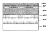
実施形態1の液晶表示装置は、画像表示用の液晶表示パネルである第1の液晶表示パネルLCD1と、透過光の屈折率を制御してレンズ(レンチキュラレンズ、シリンドリカルレンズアレイ)として機能する第2の液晶表示パネルLCD2とを備える構成となっている。この構成からなる実施形態1の液晶表示装置は、図1に示すように、バックライトユニット(バックライト装置)BLUから順番に、第1の液晶表示パネルLCD1、及び第2の液晶表示パネルLCD2がそれぞれ重ねて配置されている。すなわち、第1の液晶表示パネルLCD1の表示面側(観察者側)に第2の液晶表示パネルLCD2が配置されている。このとき、第1の液晶表示パネルLCD1と第2の液晶表示パネルLCD2との位置合わせがずれるのを防止するために、第1の液晶表示パネルLCD1と第2の液晶表示パネルLCD2とは接着部材ADHにより固定されている。なお、接着部材ADHとしては、周知の樹脂部材等からなり、第1基板SUB11,SUB21及び第2基板SUB12,SUB22として使用する透明基板(例えば、ガラス基板)と略同等の屈折率を有する部材を用いる。 The liquid crystal display device of Embodiment 1 has a first liquid crystal display panel LCD1 that is a liquid crystal display panel for image display, and a second that functions as a lens (lenticular lens, cylindrical lens array) by controlling the refractive index of transmitted light. The liquid crystal display panel LCD2 is provided. As shown in FIG. 1, the liquid crystal display device according to the first embodiment configured as described above includes a first liquid crystal display panel LCD1 and a second liquid crystal display panel LCD2 in order from a backlight unit (backlight device) BLU. They are placed one on top of the other. That is, the second liquid crystal display panel LCD2 is disposed on the display surface side (observer side) of the first liquid crystal display panel LCD1. At this time, the first liquid crystal display panel LCD1 and the second liquid crystal display panel LCD2 are bonded to each other in order to prevent misalignment between the first liquid crystal display panel LCD1 and the second liquid crystal display panel LCD2. It is fixed by ADH. The adhesive member ADH is a member made of a known resin member or the like and having a refractive index substantially equal to that of a transparent substrate (for example, a glass substrate) used as the first substrate SUB11, SUB21 and the second substrate SUB12, SUB22. Use.
実施形態1の第2の液晶表示パネルLCD2は、例えば、ねじれネマティック方式(以下、TN(Twisted Nematic)方式と記す)の液晶表示パネルで形成されており、各電極(短冊状電極)に電圧を印加しない状態で第1の液晶表示パネルLCD1からの出射光(表示画像)をそのままで透過(通過)させる2D表示となり、電圧の印加により第1の液晶表示パネルLCD1からの出射光(表示画像)を観察者の左右眼に別々入射させる両眼視差を与えるための視差障壁となるレンズ作用を行う3D表示となる。このように、実施形態1の第2の液晶表示パネルLCD2は、液晶に電界を印加しない状態においては入射光をそのまま透過させる液晶表示パネルであり、その詳細については後に詳述する。ただし、第2の液晶表示パネルLCD2はTN方式に限定されることはなく、他の方式であってもよい。 The second liquid crystal display panel LCD2 of the first embodiment is formed of, for example, a twisted nematic liquid crystal display panel (hereinafter referred to as TN (Twisted Nematic) system), and a voltage is applied to each electrode (strip-shaped electrode). In a state where no voltage is applied, 2D display is performed in which light (display image) emitted from the first liquid crystal display panel LCD1 is transmitted (passed) as it is, and light emitted from the first liquid crystal display panel LCD1 (display image) is applied by applying a voltage. Becomes a 3D display that performs a lens function as a parallax barrier for giving binocular parallax to separately enter the left and right eyes of the observer. As described above, the second liquid crystal display panel LCD2 of the first embodiment is a liquid crystal display panel that transmits incident light as it is when no electric field is applied to the liquid crystal, and details thereof will be described later. However, the second liquid crystal display panel LCD2 is not limited to the TN system, and may be another system.
また、第1の液晶表示パネルLCD1は、TN方式の液晶表示パネル、VA(Vertical Alignment)方式の液晶表示パネル、及びIPS(In-Plane Switching)方式の液晶表示パネル等の何れの方式の液晶表示パネルを用いる構成であってもよい。なお、第1の液晶表示パネルLCD1は周知の液晶表示パネルとなるので、拡散板等の光学シートや偏光板等は省略する。 The first liquid crystal display panel LCD1 is any type of liquid crystal display such as a TN liquid crystal display panel, a VA (Vertical Alignment) liquid crystal display panel, and an IPS (In-Plane Switching) liquid crystal display panel. The structure using a panel may be sufficient. Since the first liquid crystal display panel LCD1 is a well-known liquid crystal display panel, an optical sheet such as a diffusion plate, a polarizing plate, and the like are omitted.
〈第1の液晶表示パネルの構成〉
図2は本発明の実施形態1の表示装置を構成する第1の液晶表示パネルの概略構成を説明するための図、図3は実施形態1の第1の液晶表示パネルにおける第1基板側の薄膜トランジスタ構成を形成するための図、図4は実施形態1の第1の液晶表示パネルにおける画素構成を説明するための図である。ただし、図中に示すX,Yは、それぞれX軸,Y軸を示す。
<Configuration of first liquid crystal display panel>
FIG. 2 is a diagram for explaining a schematic configuration of a first liquid crystal display panel constituting the display device according to the first embodiment of the present invention. FIG. 3 is a diagram illustrating a first substrate side of the first liquid crystal display panel according to the first embodiment. FIG. 4 is a diagram for explaining a pixel configuration in the first liquid crystal display panel of the first embodiment. However, X and Y shown in the figure indicate the X axis and the Y axis, respectively.
図2に示すように、実施形態1の液晶表示パネルLCD1は周知の液晶表示パネルであり、液晶層LCを介して、ガラス基板等の周知の一対の透明基板(第1基板SUB11,第2基板SUB12)が対向配置される構成となっている。第1基板SUB11には周知の薄膜トランジスタや画素電極等が形成され、第2基板SUB12にはカラーフィルタや周知のブラックマトリクス等が形成されている。このとき、例えば、第1基板SUB11は第2基板SUB12よりも大きな透明基板で形成され、周辺部に外部との接続のための接続端子等が形成されている。また、第1基板SUB11と第2基板SUB12と固定及び液晶の封止は、第2基板SUB12の周辺部に沿って環状に塗布された周知のシール材で固定され、液晶も封止される。さらには、第1基板SUB11のバックライト装置側(液晶側の面と対向する面)には、第1の偏光板POL1が配置され、第2基板SUB12の表示面側(液晶側の面と対向する面)には、第2の偏光板POL2が配置され、第1の偏光板POL1と第2の偏光板POL2は偏光方向が90°をなすように配置されている。 As shown in FIG. 2, the liquid crystal display panel LCD1 of Embodiment 1 is a well-known liquid crystal display panel, and a pair of well-known transparent substrates (first substrate SUB11, second substrate) such as a glass substrate through a liquid crystal layer LC. SUB12) are arranged to face each other. A known thin film transistor, a pixel electrode, and the like are formed on the first substrate SUB11, and a color filter, a known black matrix, and the like are formed on the second substrate SUB12. At this time, for example, the first substrate SUB11 is formed of a transparent substrate larger than the second substrate SUB12, and a connection terminal for connection with the outside is formed in the peripheral portion. Further, the first substrate SUB11 and the second substrate SUB12 are fixed and the liquid crystal is sealed with a well-known sealing material applied in an annular shape along the periphery of the second substrate SUB12, and the liquid crystal is also sealed. Further, the first polarizing plate POL1 is disposed on the backlight device side (surface facing the liquid crystal side) of the first substrate SUB11, and the display surface side (facing the surface on the liquid crystal side) of the second substrate SUB12. The second polarizing plate POL2 is disposed on the surface of the first polarizing plate POL1, and the first polarizing plate POL1 and the second polarizing plate POL2 are disposed so that the polarization direction is 90 °.
ただし、実施形態1の液晶表示パネルLCD1では、液晶が封入された領域の内で、カラー表示用の赤(R),緑(G),青(B)の各副画素からなる画素領域(以下、画素と略記する)の形成される領域が表示領域となる。従って、液晶が封入されている領域内であっても、画素が形成されておらず表示に係わらない領域は表示領域とはならない。 However, in the liquid crystal display panel LCD1 according to the first embodiment, a pixel region (hereinafter, referred to as red (R), green (G), and blue (B) sub-pixels for color display within the region in which the liquid crystal is sealed. The region where the pixel is abbreviated as a pixel becomes a display region. Therefore, even in the region where the liquid crystal is sealed, a region where pixels are not formed and which is not involved in display is not a display region.
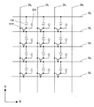
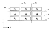
実施形態1の液晶表示パネルLCD1では、図3に示すように、第1基板SUB11の液晶側の面であって表示領域内には、図中X方向に延在しY方向に並設されるゲート線GLが形成されている。また、図中Y方向に延在しX方向に並設されるドレイン線DLが形成されている。ドレイン線DLとゲート線GLとで囲まれる矩形状の領域は、第2基板SUB12に形成される赤(R),緑(G),青(B)のカラーフィルタに対応しており、このRGBの3つの副画素SPLからなる各画素が、図4に示すように、表示領域内においてマトリックス状に配置される。なお、実施形態1においては、RGBの各副画素SPLがY方向に並設される構成としたが、これに限定されることはなく、RGBの各副画素SPLがX方向に並設される構成等の他の配列であってもよい。 In the liquid crystal display panel LCD1 of the first embodiment, as shown in FIG. 3, the liquid crystal side surface of the first substrate SUB11 extends within the display area in the X direction and is juxtaposed in the Y direction. A gate line GL is formed. In addition, a drain line DL extending in the Y direction and arranged in parallel in the X direction is formed. The rectangular region surrounded by the drain line DL and the gate line GL corresponds to the red (R), green (G), and blue (B) color filters formed on the second substrate SUB12. Each of the three sub-pixels SPL is arranged in a matrix in the display area as shown in FIG. In the first embodiment, the RGB subpixels SPL are arranged in the Y direction. However, the present invention is not limited to this, and the RGB subpixels SPL are arranged in the X direction. Other arrangements such as configuration may be used.
各副画素SPLは、例えば、ゲート線GLからの走査信号によってオンされる薄膜トランジスタTFTと、このオンされた薄膜トランジスタTFT及び該薄膜トランジスタTFTのソース線に接続されるコンタクトホールCHを介してドレイン線DLからの階調信号(階調電圧)が供給される図示しない画素電極と、隣接するゲート線GLとの間に形成される寄生容量Csとを備えている。また、IPS方式の液晶表示パネルの場合には、薄膜トランジスタTFTが形成される側の第1基板SUB11に、階調信号の電位に対して基準となる電位を有する共通信号が供給される図示しない共通電極を備える。また、VA方式やTN方式の液晶表示パネルの場合には、第2基板SUB12の側に、カラーフィルタ等と共に共通電極が形成される。 Each sub-pixel SPL includes, for example, a thin film transistor TFT that is turned on by a scanning signal from the gate line GL, and a drain line DL through the turned-on thin film transistor TFT and a contact hole CH connected to the source line of the thin film transistor TFT. The pixel electrode (not shown) to which the grayscale signal (grayscale voltage) is supplied and a parasitic capacitance Cs formed between the adjacent gate lines GL are provided. In the case of an IPS liquid crystal display panel, a common signal (not shown) is supplied to the first substrate SUB11 on the side where the thin film transistor TFT is formed. With electrodes. In the case of a VA mode or TN mode liquid crystal display panel, a common electrode is formed on the second substrate SUB12 side together with a color filter or the like.
〈第2の液晶表示パネルの構成〉
図5は本発明の表示装置における第2の液晶表示パネルの詳細構成を説明するための平面図、図6は図5に示すA−A’線での断面図であり、以下、図5及び図6に基づいて、実施形態1の第2の液晶表示パネルについて詳細に説明する。ただし、図中に示すX,Y,Zは、それぞれX軸,Y軸,Z軸を示す。
<Configuration of second liquid crystal display panel>
FIG. 5 is a plan view for explaining the detailed configuration of the second liquid crystal display panel in the display device of the present invention. FIG. 6 is a cross-sectional view taken along the line AA ′ shown in FIG. The second liquid crystal display panel of Embodiment 1 will be described in detail based on FIG. However, X, Y, and Z shown in the figure indicate an X axis, a Y axis, and a Z axis, respectively.
図5に示すように、実施形態1の第2の液晶表示パネルLCD2は、Y方向に延在しX方向に並設される複数の短冊状電極PXを備え、各短冊状電極PXの一端は第2の液晶表示パネルLCD2の長辺側の一方の辺縁部に沿ってX方向に延在して形成される配線部WRに接続される構成となっている。このとき、第2の液晶表示パネルLCD2における短冊状電極PXは、例えば、ITO(Indium Tin Oxide)やZnO(酸化亜鉛)系の透明電極で形成され、配線部WRは透明電極に限定されない。この構成により、後に詳述するように、実施形態1の第2の液晶表示パネルLCD2では、隣接して配置される一対の短冊状電極PXの間にY方向に延在するシリンドリカルレンズがX方向に並設され、レンチキュラル状にシリンドリカルレンズアレイが形成される。このとき、第2の液晶表示パネルLCD2のシリンドリカルレンズアレイが形成される領域は、第1の液晶表示パネルLCD1の表示領域に対応する位置である。その結果、実施形態1の液晶表示装置では、観察者の左右両眼がX方向に並んでいる場合に、異なる画素の光すなわち異なる視点の画像を観察者の左右両眼にそれぞれ振り分けることが可能となり、立体視が可能となる。 As shown in FIG. 5, the second liquid crystal display panel LCD2 of Embodiment 1 includes a plurality of strip electrodes PX extending in the Y direction and arranged in parallel in the X direction, and one end of each strip electrode PX is The second liquid crystal display panel LCD2 is configured to be connected to a wiring portion WR formed to extend in the X direction along one edge portion on the long side. At this time, the strip electrode PX in the second liquid crystal display panel LCD2 is formed of, for example, an ITO (Indium Tin Oxide) or ZnO (zinc oxide) based transparent electrode, and the wiring portion WR is not limited to the transparent electrode. With this configuration, as will be described in detail later, in the second liquid crystal display panel LCD2 of the first embodiment, the cylindrical lens extending in the Y direction between a pair of adjacent strip electrodes PX is disposed in the X direction. The cylindrical lens array is formed in a lenticular shape. At this time, the area where the cylindrical lens array of the second liquid crystal display panel LCD2 is formed is a position corresponding to the display area of the first liquid crystal display panel LCD1. As a result, in the liquid crystal display device of Embodiment 1, when the left and right eyes of the observer are aligned in the X direction, it is possible to distribute light of different pixels, that is, images of different viewpoints, to the left and right eyes of the observer. Thus, stereoscopic viewing is possible.
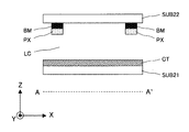
このとき、図6のA−A’線での断面図に示すように、実施形態1の第2の液晶表示パネルLCD2は、液晶(液晶層)LCを介して一対の透明基板(第1基板SUB21,第2基板SUB22)が対向配置される構成となっている。図中上側に配置される第2基板22の対向面側(液晶側の面)には、例えば、周知のブラックマトリクス等の樹脂部材からなり、Y方向に延在しX方向に並設される遮光部BMが形成されている。この遮光部BMの上層すなわち液晶側には、短冊状電極PXが形成されている。また、実施形態1の遮光部BMでは、短冊状電極PXの並設方向に対する幅が当該短冊状電極PXと同じ幅となる。 At this time, as shown in the cross-sectional view taken along the line AA ′ in FIG. 6, the second liquid crystal display panel LCD2 of the first embodiment has a pair of transparent substrates (first substrates) via the liquid crystal (liquid crystal layer) LC. The SUB21 and the second substrate SUB22) are arranged to face each other. The opposing surface side (liquid crystal side surface) of the second substrate 22 disposed on the upper side in the drawing is made of, for example, a resin member such as a known black matrix, and extends in the Y direction and is arranged in parallel in the X direction. A light shielding part BM is formed. A strip-shaped electrode PX is formed on the light shielding portion BM, that is, on the liquid crystal side. Further, in the light shielding part BM of the first embodiment, the width of the strip electrodes PX with respect to the juxtaposition direction is the same as that of the strip electrodes PX.
なお、前述のように、短冊状電極PXと遮光部BMとは近接して配置したほうが、視差が生じず透過率が高くなるために、近接して配置することが望ましいが、これに限定されることはなく、短冊状電極PXと遮光部BMを別々の透明基板(第1基板SUB21,第2基板SUB22)に形成する構成であってもよい。また、遮光部BMの形成材料は、ブラックマトリクス等と同様の樹脂材料に限定されることはなく、遮光性を有する他の材料であってもよい。さらには、短冊状電極PXの断面形状は矩形状に限定されることはなく、他の形状であってもよい。例えば、斜め方向に電界が生じるように、台形や円弧状としてもよい。 As described above, it is desirable to dispose the strip-shaped electrode PX and the light-shielding portion BM close to each other because the parallax does not occur and the transmittance increases. However, the arrangement is limited to this. The strip electrode PX and the light shielding part BM may be formed on separate transparent substrates (the first substrate SUB21 and the second substrate SUB22). Further, the material for forming the light shielding portion BM is not limited to the same resin material as that of the black matrix or the like, and may be another material having a light shielding property. Furthermore, the cross-sectional shape of the strip electrode PX is not limited to a rectangular shape, and may be another shape. For example, it may be trapezoidal or arcuate so that an electric field is generated in an oblique direction.
一方、第1基板SUB21の対向面側(液晶側の面)には、ITOやZnO等の透明導電膜で形成される平板状の電極(対向電極)CTが形成されている。このように、実施形態1の第2の液晶表示パネルLCD2では、短冊状電極PXと遮光部BMとを重ねて形成することにより、後に詳述するように、短冊状電極PXの形成個所における屈折率の乱れに伴うクロストークの影響を大幅に低減することが可能となるので、3D表示時における画質を大幅に向上することが可能となる。 On the other hand, a flat electrode (counter electrode) CT formed of a transparent conductive film such as ITO or ZnO is formed on the opposite surface side (liquid crystal side surface) of the first substrate SUB21. As described above, in the second liquid crystal display panel LCD2 of the first embodiment, the strip-shaped electrode PX and the light shielding portion BM are formed so as to overlap each other, and as described in detail later, the refraction at the portion where the strip-shaped electrode PX is formed. Since it is possible to significantly reduce the influence of crosstalk due to rate fluctuations, it is possible to greatly improve the image quality during 3D display.
〈第2の液晶表示パネルの詳細説明〉
次に、図7に従来の第2の液晶表示パネルにおける液晶分子の配向状態を説明するための図、図8に従来の第2の液晶表示パネルにおける短冊状電極位置と液晶レンズの屈折率との関係を説明するための図、図9に本発明の実施形態1の第2の液晶表示パネルにおける短冊状電極と液晶レンズの屈折率との関係説明するため図、図10に液晶レンズを用いた3D表示時の観察者と第1の液晶表示パネルとの関係を説明するため図を示し、以下、図7〜図10に基づいて、実施形態1の液晶表示装置による3D表示について説明する。ただし、図7(a)は短冊状電極と対向電極とに電界を印加した3D表示時における液晶レンズの形成部分での電界の状態を示す図であり、図7(b)は短冊状電極と対向電極とに電界を印加しない2D表示時における液晶レンズの形成部分での液晶分子の状態を示す図であり、図7(c)は短冊状電極と対向電極とに電界を印加した3D表示時における液晶レンズの形成部分での液晶分子の状態を示す図である。
<Detailed description of second liquid crystal display panel>
Next, FIG. 7 is a diagram for explaining the alignment state of the liquid crystal molecules in the conventional second liquid crystal display panel, and FIG. 8 is a diagram illustrating the position of the strip-shaped electrode and the refractive index of the liquid crystal lens in the conventional second liquid crystal display panel. FIG. 9 is a diagram for explaining the relationship, FIG. 9 is a diagram for explaining the relationship between the strip electrode and the refractive index of the liquid crystal lens in the second liquid crystal display panel of Embodiment 1 of the present invention, and FIG. 10 uses the liquid crystal lens. 3A and 3B are diagrams for explaining the relationship between the observer and the first liquid crystal display panel at the time of 3D display. Hereinafter, 3D display by the liquid crystal display device of Embodiment 1 will be described with reference to FIGS. However, FIG. 7A is a diagram showing the state of the electric field at the liquid crystal lens forming portion during 3D display in which an electric field is applied to the strip electrode and the counter electrode, and FIG. FIG. 7C is a diagram illustrating a state of liquid crystal molecules in a liquid crystal lens forming portion during 2D display in which an electric field is not applied to the counter electrode, and FIG. It is a figure which shows the state of the liquid crystal molecule | numerator in the formation part of the liquid crystal lens in.
図7(a)に示すように、従来の第2の液晶表示パネルLCD3は、観察者側に配置される第2基板SUB32の対向面側に透明導電材料からなる短冊状電極PXが形成され、液晶層LCを介して対向配置される第1基板SUB31の対向面側に透明導電材料からなる平板状の対向電極CTが形成されている。このような構成からなる従来の第2の液晶表示パネルLCD3を用いた液晶表示装置において、2D表示を行う場合には、第1の液晶表示パネルLCD1には2D表示に対応した画像、すなわち従来の2D表示と同じ画像が表示される。このときは、第1の液晶表示パネルLCD1の観察者側に配置される第2の液晶表示パネルLCD2では、短冊状電極PXと対向電極CTとには同じ電圧が印加され、その間には電界が生じない構成となる。その結果、図7(b)に示すように、液晶分子LCは初期配向状態のままとなり、第1の液晶表示パネルLCD1の全ての画素からの表示光が観察者の左右の目に到達し、2D表示の画像が認識されることとなる。
As shown in FIG. 7A, in the conventional second liquid crystal display panel LCD3, strip-like electrodes PX made of a transparent conductive material are formed on the opposite surface side of the second substrate SUB32 disposed on the viewer side. A plate-like counter electrode CT made of a transparent conductive material is formed on the opposite surface side of the first substrate SUB31 that is opposed to the liquid crystal layer LC. In the liquid crystal display device using the conventional second liquid crystal
一方、3D表示を行う場合には、実施形態1の第2の液晶表示パネルLCD2では、図7(a)に示すように、短冊状電極PXと対向電極CTとの間に矢印で示す電界EFを印加することによって、隣接配置される各短冊状電極PXとの間にY方向に延在しX方向に並設されるシリンドリカルレンズを形成する構成としている。すなわち、図7(c)に示すように、短冊状電極PXと対向電極CTとの間に印加される電界EFにより、液晶分子の配向方向を制御し、その屈折率を隣接する短冊状電極PXとの間で変化させ、シリンドリカルレンズを形成している。 On the other hand, when performing 3D display, in the second liquid crystal display panel LCD2 of Embodiment 1, as shown in FIG. 7A, an electric field EF indicated by an arrow between the strip electrode PX and the counter electrode CT. Is applied to form a cylindrical lens extending in the Y direction and juxtaposed in the X direction between each adjacent strip-shaped electrode PX. That is, as shown in FIG. 7C, the orientation direction of the liquid crystal molecules is controlled by the electric field EF applied between the strip electrode PX and the counter electrode CT, and the refractive index thereof is changed to the adjacent strip electrode PX. To form a cylindrical lens.
ここで、本願発明者は、図7(a)に示すように、短冊状電極PXが形成される領域では、電界EFの方向がX方向に対して反対方向となるために液晶分子LCの配向方向の制御が困難となり、点線Bで示す領域に液晶配向の乱れであるディスクリネーションが生じ、その結果、屈折率分布が乱れてしまうことを発見した。図8に示す従来構成の1つのシリンドリカルレンズを形成するための一対の短冊状電極PX間におけるX方向の屈折率の計測結果のグラフG1から明らかなように、隣接する短冊状電極PXとの間である区間P2〜区間P3においてはシリンドリカルレンズが形成される。これに対して、短冊状電極PXが形成される区間P1〜区間P2及び区間P3〜区間P4では、液晶レンズであるシリンドリカルレンズの屈折率が大きく乱れてしまい、その結果、クロストークが増大してしまうことが判明した。 Here, as shown in FIG. 7A, the inventor of the present application has the alignment of the liquid crystal molecules LC because the direction of the electric field EF is opposite to the X direction in the region where the strip electrode PX is formed. It has been found that the control of the direction becomes difficult, and disclination, which is a disorder of the liquid crystal alignment, occurs in the region indicated by the dotted line B. As a result, the refractive index distribution is disturbed. As is apparent from the graph G1 of the measurement result of the refractive index in the X direction between the pair of strip-shaped electrodes PX for forming one cylindrical lens having the conventional configuration shown in FIG. 8, it is between the adjacent strip-shaped electrodes PX. A cylindrical lens is formed in the section P2 to the section P3. On the other hand, in the section P1 to the section P2 and the section P3 to the section P4 where the strip-shaped electrode PX is formed, the refractive index of the cylindrical lens that is a liquid crystal lens is greatly disturbed, and as a result, crosstalk increases. It turned out to be.
このように、本願発明者らは液晶パネルを用いて形成したシリンドリカルレンズアレイの特性を計測し、隣接するレンズ(シリンドリカルレンズ)との境界部分で生じる液晶分子の配向乱れが最も大きな原因であることを突き止めた。すなわち、それぞれのシリンドリカルレンズを形成するための電界を印加する短冊状電極の内で、隣接するレンズ間に形成される電極部分では、短冊状電極と面状電極との間の領域にディスクリネーションすなわち液晶分子の配向乱れが発生し、この配向乱れにより屈折率分布がレンズ形状とならないために、クロストークが生じてしまう。 As described above, the inventors of the present application measured the characteristics of the cylindrical lens array formed using the liquid crystal panel, and the disorder of alignment of liquid crystal molecules generated at the boundary portion with the adjacent lens (cylindrical lens) is the largest cause. I found out. That is, among the strip electrodes that apply an electric field for forming each cylindrical lens, the electrode portion formed between adjacent lenses has a disclination in the region between the strip electrode and the planar electrode. That is, the alignment disorder of the liquid crystal molecules occurs, and this alignment disorder causes the refractive index distribution not to have a lens shape, thereby causing crosstalk.
従って、実施形態1の第2の液晶表示パネルLCD2では、前述する図6に示すように、短冊状電極PXに重畳して遮光部BMを形成する構成としているので、図9に示す実施形態1の第2の液晶表示パネルLCD2におけるシリンドリカルレンズを形成するための一対の短冊状電極PX間でのX方向の屈折率の計測結果のグラフG2から明らかなように、一対の短冊状電極PXとの間の区間P2〜区間P3においてはシリンドリカルレンズを形成することができると共に、短冊状電極PXが形成される区間P1〜区間P2及び区間P3〜区間P4の領域では屈折率の乱れた表示光を遮蔽している。その結果、実施形態1の第2の液晶表示パネルLCD2では、クロストークを低減させた視差障壁となるシリンドリカルレンズを形成することが可能となり、3D表示時における画質を向上させることが可能となる。このとき、従来の構成では6%のクロストークが生じていたが、実施形態1の液晶表示装置ではクロストークを3%に半減させることができる。なお、屈折率は、位置の二次関数で変化することが好ましいが、二次関数の屈折率からずれていてもクロストークが生じない程度に屈折率分布が生じていればよい。例えば、2視点の場合には、レンズ中心では屈折率変化が小さくてもクロストークは小さいからである。 Therefore, in the second liquid crystal display panel LCD2 of the first embodiment, as shown in FIG. 6 described above, the light shielding portion BM is formed so as to overlap the strip-shaped electrode PX, so that the first embodiment shown in FIG. As apparent from the graph G2 of the measurement result of the refractive index in the X direction between the pair of strip electrodes PX for forming the cylindrical lens in the second liquid crystal display panel LCD2, the relationship between the pair of strip electrodes PX and In the interval P2 to interval P3, a cylindrical lens can be formed, and display light with a disordered refractive index is shielded in the interval P1 to interval P2 and the interval P3 to interval P4 where the strip electrode PX is formed. doing. As a result, in the second liquid crystal display panel LCD2 of Embodiment 1, it is possible to form a cylindrical lens serving as a parallax barrier with reduced crosstalk, and to improve the image quality during 3D display. At this time, the crosstalk of 6% occurred in the conventional configuration, but the crosstalk can be reduced to half by 3% in the liquid crystal display device of the first embodiment. Note that the refractive index is preferably changed by a quadratic function of the position, but it is sufficient that the refractive index distribution is generated to such an extent that crosstalk does not occur even if the refractive index deviates from the refractive index of the quadratic function. For example, in the case of two viewpoints, even if the refractive index change is small at the center of the lens, the crosstalk is small.
また、実施形態1の表示装置では、観察者の両眼に視差を与えることによって裸眼3D表示を可能としているので、短冊状電極PXの間隔は、例えば、図10に示すように、観察者の右目REには第1の液晶表示パネルLCD1に表示される右目用画像Rが入射され、左目LEには左目用画像Lが入射されるように形成されている。ただし、短冊状電極PXの間隔は、観察者の視点位置に応じて変化することとなるので、左右の目の間隔B、第1の液晶表示パネルLCD1の画素ピッチP、第2の液晶表示パネルLCD2に形成されるレンズLZのピッチ(レンズピッチ)Qの間には、下記の式1に示す関係がある。 Further, in the display device of the first embodiment, since the naked eye 3D display is enabled by giving parallax to both eyes of the observer, the interval between the strip electrodes PX is, for example, as shown in FIG. A right eye image R displayed on the first liquid crystal display panel LCD1 is incident on the right eye RE, and a left eye image L is incident on the left eye LE. However, since the interval between the strip electrodes PX changes according to the viewpoint position of the observer, the interval B between the left and right eyes, the pixel pitch P of the first liquid crystal display panel LCD1, and the second liquid crystal display panel. Between the pitches (lens pitches) Q of the lenses LZ formed on the LCD 2, there is a relationship expressed by the following formula 1.
(数1)
Q=2P/(1+P/B) ・・・(式1)
従って、実施形態1の液晶表示装置を構成する第1の液晶表示パネルLCD1と第2の液晶表示パネルLCD2とは、予め設定した視点に対して、式1に従った画素ピッチP及びレンズピッチQを有する構成となっている。なお、実施形態1の液晶表示装置は2視点に限定されることはなく、2視点以上の他視点方式にも応用できるものである。
(Equation 1)
Q = 2P / (1 + P / B) (Formula 1)
Therefore, the first liquid crystal display panel LCD1 and the second liquid crystal display panel LCD2 constituting the liquid crystal display device of the first embodiment have a pixel pitch P and a lens pitch Q according to Equation 1 with respect to a preset viewpoint. It has composition which has. Note that the liquid crystal display device of Embodiment 1 is not limited to two viewpoints, and can be applied to other viewpoint systems with two or more viewpoints.
図11は本発明の表示装置である液晶表示装置における遮光部占有率とモアレ強度との計測結果を示す図、図12は本発明の表示装置である液晶表示装置における電極占有率とクロストークとの計測結果を示す図である。特に、図11に示すモアレ強度はモアレの見えやすさを示しており、遮光部占有率cは遮光部BMのX方向幅SとレンズピッチQとから、c=S/Qで定義される。また、図12に示す電極占有率rは、短冊状電極PXのX方向幅WとレンズピッチQとから、r=W/Qで定義される。 FIG. 11 is a diagram showing the measurement results of the light shielding portion occupancy and the moire intensity in the liquid crystal display device which is the display device of the present invention, and FIG. 12 is the electrode occupancy and crosstalk in the liquid crystal display device which is the display device of the present invention. It is a figure which shows the measurement result. In particular, the moiré intensity shown in FIG. 11 indicates the visibility of the moiré, and the light shielding portion occupation ratio c is defined by c = S / Q from the X-direction width S of the light shielding portion BM and the lens pitch Q. Further, the electrode occupation ratio r shown in FIG. 12 is defined by r = W / Q from the width W in the X direction of the strip electrode PX and the lens pitch Q.
図11のグラフG3から明らかなように、モアレの強度は、画素の輝度変化とレンズ電極による透過率変化の基本空間周波数における振幅に比例する。すなわち、電極幅を小さくすると、基本空間周波数での振幅が小さくなるためモアレが発生しにくくなる。従って、モアレを発生させないためには、遮光部BMの幅すなわち遮光幅は小さいことが望ましい。一方、モアレを気にならない程度に低減するためには、モアレ強度を0.3以下とする必要があり、グラフG3から遮光部占有率は0.1以下とすることが望ましい。また、バリア方式の3Dに用いられる電極占有率0.5のITO電極と同程度のモアレ強度0.15以下とするためには,遮光部占有率は0.05以下とすることが望ましい。 As is apparent from the graph G3 in FIG. 11, the intensity of the moire is proportional to the amplitude at the basic spatial frequency of the luminance change of the pixel and the transmittance change by the lens electrode. That is, when the electrode width is reduced, the amplitude at the basic spatial frequency is reduced, so that moire is less likely to occur. Therefore, in order not to generate moire, it is desirable that the width of the light shielding portion BM, that is, the light shielding width is small. On the other hand, in order to reduce the moire to such an extent that it does not matter, it is necessary to make the moire intensity 0.3 or less, and it is desirable from the graph G3 that the light shielding portion occupation ratio is 0.1 or less. Further, in order to make the moiré intensity 0.15 or less comparable to that of the ITO electrode having an electrode occupancy ratio of 0.5 used in 3D of the barrier method, it is desirable that the light shielding portion occupancy ratio is 0.05 or less.
また、図12に示す短冊状電極PXの幅と遮光部BMの幅とが同じ実施形態1においては、電極幅と遮光部幅とが同じ場合のグラフG6から明らかなように、電極占有率を0.05以上とすることが望ましい。 In the first embodiment in which the width of the strip-shaped electrode PX and the width of the light shielding portion BM shown in FIG. 12 are the same, as is apparent from the graph G6 when the electrode width and the light shielding portion width are the same, the electrode occupation ratio is It is desirable to set it as 0.05 or more.
以上説明したように、実施形態1の表示装置である液晶表示装置では、画像表示を行う第1の液晶表示パネルLCD1の表示面側に第2の液晶表示パネルLCD2を配置され、3D表示時には第2の液晶表示パネルLCD2に視差障壁となるシリンドリカルレンズを形成すると共に、第1の液晶表示パネルLCD1に3D表示に対応した映像を表示させる構成となっている。 As described above, in the liquid crystal display device that is the display device of the first embodiment, the second liquid crystal display panel LCD2 is arranged on the display surface side of the first liquid crystal display panel LCD1 that performs image display. A cylindrical lens serving as a parallax barrier is formed on the second liquid crystal display panel LCD2, and an image corresponding to 3D display is displayed on the first liquid crystal display panel LCD1.
また、第2の液晶表示パネルLCD2の一方の透明基板に短冊状電極PXが形成され、液晶層を介して対向配置される他方の透明基板に平板状の対向電極CTが形成され、3D表示時には短冊状電極PXと対向電極CTとの間に電界を印加して短冊状電極PXの延在方向に延在すると共に、その並設方向に並設されるシリンドリカルレンズを形成することにより、3D表示時における視差障壁としており、さらには、短冊状電極PXに沿って重ねて形成される遮光部が形成される構成となっているので、液晶分子の配向乱れに伴う屈折率分布の乱れる領域を通過する表示光を遮光することができるので、3D表示時におけるクロストークを大幅に低減させることが可能となり、その結果、3D表示画像を高画質で表示させることが可能となる。 Further, a strip-like electrode PX is formed on one transparent substrate of the second liquid crystal display panel LCD2, and a flat counter electrode CT is formed on the other transparent substrate opposed to each other via a liquid crystal layer. By applying an electric field between the strip electrode PX and the counter electrode CT to extend in the extending direction of the strip electrode PX, and forming a cylindrical lens arranged in parallel in the parallel direction, 3D display Since it is a parallax barrier at the time, and further, a light-shielding part is formed so as to overlap with the strip-shaped electrode PX, it passes through a region where the refractive index distribution is disturbed due to disorder of alignment of liquid crystal molecules Therefore, the crosstalk during 3D display can be greatly reduced, and as a result, a 3D display image can be displayed with high image quality.
また、実施形態1の第2の液晶表示パネルLCD2では、図13(a)に示すように、第2基板SUB22の表面に近い側に遮蔽部BMを形成し、該遮蔽部BMの上層に側に対向電極CTを形成する構成としたが、これに限定されることはない。例えば、図13(b)に示すように、第2基板SUB22に近い側に短冊状電極PXを形成し、該短冊状電極PXの上層に遮光部BMを形成する構成であってもよい。また、図13(c)に示すように、第2基板SUB22の側に平板状の対向電極CTを形成し、第1基板SUB21の側に遮光部BMと短冊状電極PXとをこの順番で形成する構成であってもよい。さらには、図13(d)に示すように、第2基板SUB22の側に平板状の対向電極CTを形成し、第1基板SUB21の側に短冊状電極PXと遮光部BMとをこの順番で形成する構成であってもよい。特に、図13(b)や図13(d)に示すように、短冊状電極PXよりも液晶層LCの側に遮光部BMを形成する場合には、遮光部BMをレジストとして短冊状電極PXをエッチングすることができるので、遮光部BMの形成に伴う製造工程の増加を防止することができるという格別の効果を得ることができる。 Further, in the second liquid crystal display panel LCD2 of the first embodiment, as shown in FIG. 13A, the shielding part BM is formed on the side close to the surface of the second substrate SUB22, and the upper side of the shielding part BM is on the side. However, the present invention is not limited to this. For example, as shown in FIG. 13B, a configuration in which the strip electrode PX is formed on the side close to the second substrate SUB22 and the light shielding portion BM is formed in the upper layer of the strip electrode PX may be employed. Further, as shown in FIG. 13C, the flat counter electrode CT is formed on the second substrate SUB22 side, and the light shielding portion BM and the strip electrode PX are formed in this order on the first substrate SUB21 side. It may be configured to. Furthermore, as shown in FIG. 13D, a flat counter electrode CT is formed on the second substrate SUB22 side, and the strip-like electrode PX and the light shielding portion BM are arranged in this order on the first substrate SUB21 side. The structure to form may be sufficient. In particular, as shown in FIGS. 13B and 13D, when the light shielding part BM is formed on the liquid crystal layer LC side of the strip electrode PX, the strip electrode PX is formed using the light shielding part BM as a resist. Therefore, it is possible to obtain a special effect that an increase in the manufacturing process accompanying the formation of the light shielding part BM can be prevented.
〈実施形態2〉
図14は本発明の実施形態2の表示装置である液晶表示装置の概略構成を説明するための図であり、以下、図14に基づいて実施形態2の液晶表示装置について説明する。ただし、実施形態2の液晶表示装置は、第2の液晶表示パネルLCD2に形成される遮光部BMの構成を除く他の構成は実施形態1と同様となる。従って、以下の説明では、遮光部BMと短冊状電極PXとについて詳細に説明する。また、説明を簡単にするために、図14は第2基板SUB22を図中下側にし、第1基板SUB21を図中上側としている。
<Embodiment 2>
FIG. 14 is a diagram for explaining a schematic configuration of a liquid crystal display device which is a display device according to the second embodiment of the present invention. Hereinafter, the liquid crystal display device according to the second embodiment will be described with reference to FIG. However, the configuration of the liquid crystal display device according to the second embodiment is the same as that of the first embodiment except for the configuration of the light shielding portion BM formed in the second liquid crystal display panel LCD2. Therefore, in the following description, the light shielding part BM and the strip electrode PX will be described in detail. For the sake of simplicity, FIG. 14 shows the second substrate SUB22 on the lower side in the drawing and the first substrate SUB21 on the upper side in the drawing.
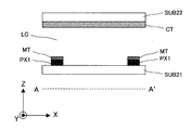
図14に示すように、実施形態2の第2の液晶表示パネルLCD2は、X方向すなわち短冊状電極PXの並設方向に対する遮光部BMの幅Sが当該短冊状電極PXの幅Wよりも小さい構成となっている。このとき、図14に示す遮光部BMのX方向側の辺縁部は短冊状電極PXのX方向側の辺縁部よりも中心に寄った構成となっている。すなわち、実施形態2の短冊状電極PXの幅Wは遮光部BMの幅Sよりも大きく形成され、当該遮光部BMのX方向に対向する辺縁部よりも短冊状電極PXの辺縁部が外側に形成されている。その結果、短冊状電極PXの液晶側面の一部が遮光部BMより露出する構成となっている。 As shown in FIG. 14, in the second liquid crystal display panel LCD2 according to the second embodiment, the width S of the light shielding part BM in the X direction, that is, the direction in which the strip-shaped electrodes PX are arranged side by side is smaller than the width W of the strip-shaped electrodes PX. It has a configuration. At this time, the edge part on the X direction side of the light shielding part BM shown in FIG. 14 is configured closer to the center than the edge part on the X direction side of the strip-shaped electrode PX. That is, the width W of the strip-shaped electrode PX of the second embodiment is formed larger than the width S of the light-shielding portion BM, and the edge portion of the strip-shaped electrode PX is larger than the edge portion facing the X direction of the light-shielding portion BM. It is formed on the outside. As a result, a part of the liquid crystal side surface of the strip electrode PX is exposed from the light shielding portion BM.
このような構成とすることにより、実施形態2の第2の液晶表示パネルLCD2では、透明電極からなる短冊状電極PXのX方向幅Wと遮光部BMのX方向幅Sとをそれぞれ異なる幅で形成することが可能となる。このとき、図12に示す透明電極のみで形成した場合の電極占有率とクロストークとの計測結果のグラフG4、及び遮光部占有率が0.06時の電極占有率とクロストークとの計測結果のグラフG5から明らかなように、電極占有率rが0.05以下、及び0.2以上の領域でクロストークが急激に増加することが分かる。電極占有率rが小さい場合は、屈折率分布の形成が不十分でクロストークが生じると考えられる。一方、電極占有率rが大きい場合は、短冊状電極PX上からクロストークが生じると考えられる。したがって、ITOの透明電極材料により短冊状電極PXを形成する場合、電極占有率rは0.05以上、又は0.2以下が望ましい。 With such a configuration, in the second liquid crystal display panel LCD2 of the second embodiment, the X-direction width W of the strip-shaped electrode PX made of a transparent electrode and the X-direction width S of the light shielding portion BM are different from each other. It becomes possible to form. At this time, the measurement result of the electrode occupancy and the crosstalk when the electrode occupancy and the crosstalk are formed with only the transparent electrode shown in FIG. 12, and the measurement result of the electrode occupancy and the crosstalk when the light shielding portion occupancy is 0.06. As can be seen from the graph G5, the crosstalk rapidly increases in the region where the electrode occupation ratio r is 0.05 or less and 0.2 or more. When the electrode occupation ratio r is small, it is considered that the refractive index distribution is not sufficiently formed and crosstalk occurs. On the other hand, when the electrode occupation ratio r is large, it is considered that crosstalk occurs from the strip electrode PX. Therefore, when the strip-shaped electrode PX is formed of the ITO transparent electrode material, the electrode occupation ratio r is desirably 0.05 or more or 0.2 or less.
すなわち、モアレの低減を重視する場合には、遮光部BMの幅Sを短冊状電極PXの幅Wよりも狭くすることが望ましい。また、遮光部BMによる遮光部占有率cは電極占有率rよりも小さく、0.1以下、特に、0.05以下とすることが望ましい。 That is, when emphasizing the reduction of moire, it is desirable to make the width S of the light-shielding portion BM narrower than the width W of the strip-shaped electrode PX. Further, the light shielding part occupation ratio c by the light shielding part BM is smaller than the electrode occupation ratio r, and is preferably 0.1 or less, particularly 0.05 or less.
ここで、実施形態2の液晶表示装置では、短冊状電極PXを透明電極材料で形成する構成としているので、グラフG4及びグラフG5並びに図11のグラフG3から明らかなように、遮光部の幅Sを狭くすることにより、モアレの発生を低減することができ、2D表示時の輝度を向上させることが可能となる。このとき、遮光部BMのX方向幅Sの下限は3D表示時のクロストークによって制約され、遮光部BMの幅の上限はモアレ及び2D表示時の輝度によって制約される。 Here, in the liquid crystal display device according to the second embodiment, since the strip-shaped electrode PX is formed of a transparent electrode material, the width S of the light-shielding portion is apparent from the graphs G4 and G5 and the graph G3 in FIG. By narrowing the width, the occurrence of moire can be reduced and the luminance during 2D display can be improved. At this time, the lower limit of the width S in the X direction of the light shielding part BM is restricted by crosstalk during 3D display, and the upper limit of the width of the light shielding part BM is restricted by moire and brightness during 2D display.
このように、実施形態2の液晶表示装置における第2の液晶表示パネルLCD2では、短冊状電極PXのX方向の幅Wよりも遮光部BMのX方向幅Sを小さくする構成となっているので、実施形態1の効果に加えて、2D表示時の輝度を向上させることが可能となる。 Thus, the second liquid crystal display panel LCD2 in the liquid crystal display device of Embodiment 2 has a configuration in which the X-direction width S of the light-shielding portion BM is smaller than the X-direction width W of the strip-shaped electrode PX. In addition to the effects of the first embodiment, the luminance during 2D display can be improved.
なお、実施形態2においては、短冊状電極PXが第2基板SUB22に近い側に形成される場合について説明したが、図13に示す実施形態1と同様に、短冊状電極PXよりも遮光部BMを第2基板SUB22に近い側に形成する構成であってもよい。さらには、第1基板SUB21に短冊状電極PXと遮光部BMとを形成し、第2基板SUB22に対向電極CTを形成する構成であってもよい。 In the second embodiment, the case where the strip-shaped electrode PX is formed on the side close to the second substrate SUB22 has been described. However, as in the first embodiment shown in FIG. May be formed on the side close to the second substrate SUB22. Further, the strip electrode PX and the light shielding part BM may be formed on the first substrate SUB21, and the counter electrode CT may be formed on the second substrate SUB22.
〈実施形態3〉
図15は本発明の実施形態3の表示装置における第2の液晶表示パネルLCD2の概略構成を説明するための図であり、特に、図15(a),(d)は短冊状電極PXと液晶分子LCのプレチルト角と初期配向方向とを示す図であり、図15(b),(e)は電界印加時の配向不良個所と短冊状電極PXとの関係を示す図であり、図15(c),(f)は短冊状電極PXと遮光部BMとの位置関係を示す図である。ただし、実施形態3の第2の液晶表示パネルLCD2は、短冊状電極PXと重ねて配置される遮光部BMのX方向の形成位置が異なるのみであり、他の構成は実施形態2と同様の構成である。従って、以下の説明では、遮光部BMの形成位置について詳細に説明する。
<
FIG. 15 is a diagram for explaining a schematic configuration of the second liquid crystal display panel LCD2 in the display device according to the third embodiment of the present invention. In particular, FIGS. 15 (a) and 15 (d) show the strip electrode PX and the liquid crystal. FIGS. 15B and 15E are diagrams showing a relationship between a misalignment portion and a strip-shaped electrode PX when an electric field is applied, and FIG. (c), (f) is a figure which shows the positional relationship of the strip electrode PX and the light-shielding part BM. However, the second liquid crystal display panel LCD2 of the third embodiment is different only in the formation position in the X direction of the light shielding portion BM arranged to overlap the strip-shaped electrode PX, and the other configuration is the same as that of the second embodiment. It is a configuration. Therefore, in the following description, the formation position of the light shielding part BM will be described in detail.
図15(a)に示すように、液晶分子LCの長軸方向がX方向に初期配向されると共に、当該液晶分子LCの長軸方向の図中右側が第2基板SUB22よりも持ち上がるようなプレチルト角を有する場合、短冊状電極PXと図示しない対向電極CTとの間に電界EFが印加されると、図15(b)に示すように、短冊状電極PXの図中左端側すなわち液晶分子LCの長軸方向の端部の内で持ち上がっていない側に配向不良個所DDPが形成される。従って、図15(c)に示すように、短冊状電極PXのX方向の図中左側端部に遮光部BMを形成することにより、前述する実施形態2の効果に加えて、遮光部BMのX方向幅を増加させることなく、効果的に配向不良個所すなわち屈折率分布が乱れる領域を遮光することができるという格別の効果を得ることが可能となる。 As shown in FIG. 15A, the pretilt in which the long axis direction of the liquid crystal molecules LC is initially aligned in the X direction and the right side of the liquid crystal molecules LC in the long axis direction is lifted from the second substrate SUB22. In the case of having a corner, when the electric field EF is applied between the strip electrode PX and the counter electrode CT (not shown), as shown in FIG. 15B, the left end side of the strip electrode PX in the drawing, that is, the liquid crystal molecule LC. The misaligned portion DDP is formed on the side of the end portion in the major axis direction that is not lifted. Therefore, as shown in FIG. 15C, by forming the light shielding part BM at the left end in the X direction of the strip-shaped electrode PX, in addition to the effect of the second embodiment, the light shielding part BM Without increasing the width in the X direction, it is possible to obtain a special effect that it is possible to effectively shield light from a poorly aligned portion, that is, a region where the refractive index distribution is disturbed.
同様にして、図15(d)に示すように、X方向に初期配向される液晶分子LCの長軸方向の図中左側が第2基板SUB22よりも持ち上がるようなプレチルト角を有する場合では、短冊状電極PXと対向電極CTとの間への電界EFの印加により、図15(e)に示すように、短冊状電極PXの図中右端側すなわち液晶分子LCの長軸方向の端部の内で持ち上がっていない側に配向不良個所DDPが形成される。従って、図15(f)に示すように、短冊状電極PXのX方向の図中右側端部に遮光部BMを形成することにより、前述する実施形態2の効果に加えて、遮光部BMのX方向幅を増加させることなく、効果的に配向不良個所すなわち屈折率分布が乱れる領域を遮光することが可能となる。 Similarly, as shown in FIG. 15D, in the case where the liquid crystal molecules LC initially aligned in the X direction have a pretilt angle such that the left side in the figure in the major axis direction is raised from the second substrate SUB22, By applying an electric field EF between the electrode PX and the counter electrode CT, as shown in FIG. 15 (e), the inside of the strip-shaped electrode PX on the right end side in the drawing, that is, the end in the major axis direction of the liquid crystal molecule LC. Thus, a misaligned portion DDP is formed on the side not lifted. Therefore, as shown in FIG. 15 ( f ), by forming the light shielding portion BM at the right end portion in the X direction of the strip-shaped electrode PX, in addition to the effects of the second embodiment, the light shielding portion BM Without increasing the width in the X direction, it is possible to effectively shield light from a poorly aligned portion, that is, a region where the refractive index distribution is disturbed.
なお、プレチルト角を有しない初期配向では、遮光部は短冊状電極PXの中央部付近に形成する。 In the initial alignment without a pretilt angle, the light shielding portion is formed in the vicinity of the central portion of the strip electrode PX.
〈実施形態4〉
図16は本発明の実施形態4の表示装置における第2の液晶表示パネルの概略構成を説明するための図であり、実施形態2とは異なり、短冊状電極PXのX方向幅Wが遮光部BMのX方向幅Sよりも小さい場合である。従って、以下の説明では、短冊状電極PXと遮光部BMとの構成について詳細に説明する。
<
FIG. 16 is a diagram for explaining a schematic configuration of the second liquid crystal display panel in the display device according to the fourth embodiment of the present invention. Unlike the second embodiment, the X-direction width W of the strip-shaped electrode PX is the light shielding portion. This is a case where it is smaller than the width S of the BM in the X direction. Therefore, in the following description, the configuration of the strip-shaped electrode PX and the light shielding part BM will be described in detail.
図16から明らかなように、実施形態4の短冊状電極PXのX方向幅Wが遮光部BMのX方向幅Sよりも小さい場合である。このとき、第2基板SUB22に近い側に短冊状電極PXが形成され、該短冊状電極PXの上層に重ねて遮光部BMを形成する構成となっているので、短冊状電極PXはX方向すなわち並設方向に対して遮光部BMに覆われる構成となる。 As is apparent from FIG. 16, the X-direction width W of the strip-shaped electrode PX of the fourth embodiment is smaller than the X-direction width S of the light shielding part BM. At this time, the strip-shaped electrode PX is formed on the side close to the second substrate SUB22, and the light-shielding portion BM is formed on the upper layer of the strip-shaped electrode PX. It becomes the structure covered with the light-shielding part BM with respect to the parallel arrangement direction.
実施形態4の液晶表示装置においても、前述する実施形態2の液晶表示装置と同様の構成となるので、図11及び図12のグラフG3〜G6から明らかなように、ITOの透明電極材料により短冊状電極PXを形成する場合、電極占有率rは0.05以上、又は0.2以下が望ましい。また、遮光部BMによる遮光部占有率cは、0.1以下、特に、0.05以下とすることが望ましい。さらには、電極占有率rは遮光部占有幅よりも大きくし,かつ0.05以上0.2以下とすることが望ましい。 Since the liquid crystal display device according to the fourth embodiment has the same configuration as that of the liquid crystal display device according to the second embodiment described above, it is apparent from the graphs G3 to G6 in FIGS. When the electrode PX is formed, the electrode occupation ratio r is preferably 0.05 or more or 0.2 or less. Further, it is desirable that the light shielding portion occupation ratio c by the light shielding portion BM is 0.1 or less, particularly 0.05 or less. Further, it is desirable that the electrode occupation ratio r is larger than the light shielding portion occupation width and is 0.05 to 0.2.
このとき、実施形態4の液晶表示装置では、遮光部BMのX方向幅Sを大きくすることが可能となるので、3D表示時におけるクロストークを大幅に低減させる、すなわち3D表示時における画質を大幅に向上させることが可能となる。
At this time, in the liquid crystal display device of
〈実施形態5〉
図17は本発明の実施形態5の表示装置である液晶表示装置の概略構成を説明するための図である。ただし、実施形態5の液晶表示装置では、第2の液晶表示パネルLCD2の短冊状電極PX1が遮光性を有する金属材料で形成される構成が異なるのみで、他の構成は実施形態1の第2の液晶表示パネルLCD2と同様となる。従って、以下の説明では、短冊状電極PX1について詳細に説明する。
<Embodiment 5>
FIG. 17 is a diagram for explaining a schematic configuration of a liquid crystal display device which is a display device according to Embodiment 5 of the present invention. However, in the liquid crystal display device of the fifth embodiment, only the configuration in which the strip-like electrode PX1 of the second liquid crystal display panel LCD2 is formed of a metal material having a light shielding property is different, and the other configuration is the second configuration of the first embodiment. This is the same as the liquid crystal display panel LCD2. Therefore, in the following description, the strip electrode PX1 will be described in detail.
図17に示すように、実施形態5の第2の液晶表示パネルLCD2においても、短冊状電極PX1はY方向に延在しX方向に並設される構成となっており、各短冊状電極PX1の一端は第2の液晶表示パネルLCD2の長辺側の一方の辺縁部に沿ってX方向に延在して形成される配線部WRに接続される構成となっている。実施形態5の第2の液晶表示パネルLCD2は、液晶(液晶層)LCを介して対向配置される一対のガラス基板等の透明基板(第1基板SUB21,第2基板SUB22)からなり、図中上側に配置される第2基板22の対向面側(液晶側の面)には、例えば、反射率の小さいCr(クロム),Mo(モリブデン),W(タングステン),Ta(タンタル),Nb(ニオブ)等又はその合金からなる金属電極材料により短冊状電極PX1が形成されている。 As shown in FIG. 17, also in the second liquid crystal display panel LCD2 of Embodiment 5, the strip electrodes PX1 extend in the Y direction and are arranged in parallel in the X direction, and each strip electrode PX1. One end of the second liquid crystal display panel LCD2 is connected to a wiring part WR formed to extend in the X direction along one long side of the second liquid crystal display panel LCD2. The second liquid crystal display panel LCD2 of Embodiment 5 includes a pair of transparent substrates (a first substrate SUB21 and a second substrate SUB22) such as a pair of glass substrates disposed to face each other via a liquid crystal (liquid crystal layer) LC. For example, Cr (chromium), Mo (molybdenum), W (tungsten), Ta (tantalum), and Nb (low reflectance) are provided on the opposite surface side (liquid crystal side surface) of the second substrate 22 disposed on the upper side. The strip electrode PX1 is formed of a metal electrode material made of niobium or the like or an alloy thereof.
従って、実施形態1と同様に、短冊状電極PX1のX方向幅が遮光領域の幅となるので、実施形態1の液晶表示装置と同様の効果を得ることが可能となる。さらには、遮光性を有する金属材料で短冊状電極PX1を形成しているので、遮光部BMを形成する工程が不要となり、製造工程を増加させることなく遮光領域を形成できるという格別の効果を得ることが可能となる。ただし、実施形態1と同様に、短冊状電極PX1の断面形状は矩形に限定されることはなく、他の形状であってもよい。例えば、斜め方向に電界が生じるように、台形や円弧状としてもよい。 Therefore, as in the first embodiment, the X-direction width of the strip-shaped electrode PX1 is the width of the light shielding region, so that the same effect as the liquid crystal display device of the first embodiment can be obtained. Furthermore, since the strip-shaped electrode PX1 is formed of a metal material having a light shielding property, a process for forming the light shielding part BM is not required, and a special effect that the light shielding region can be formed without increasing the manufacturing process is obtained. It becomes possible. However, as in the first embodiment, the cross-sectional shape of the strip-shaped electrode PX1 is not limited to a rectangle, and may be another shape. For example, it may be trapezoidal or arcuate so that an electric field is generated in an oblique direction.
また、第1基板SUB21の対向面側(液晶側の面)には、ITOやZnO等の透明導電膜で形成される平板状の電極(対向電極)CTが形成されている。 A flat electrode (counter electrode) CT formed of a transparent conductive film such as ITO or ZnO is formed on the opposite surface side (liquid crystal side surface) of the first substrate SUB21.
以上に説明した構成により、実施形態1と同様に、短冊状電極PX1の形成個所における屈折率の乱れに伴うクロストークの影響を大幅に低減することが可能となり、3D表示時における画質を大幅に向上することが可能となる。 With the configuration described above, as in the first embodiment, it is possible to greatly reduce the influence of crosstalk due to the refractive index disturbance at the location where the strip-shaped electrode PX1 is formed, and the image quality during 3D display is greatly improved. It becomes possible to improve.
また、短冊状電極PX1のX方向幅については、実施形態1と同様、図11のグラフG3から明らかなように、モアレを発生させないためには、遮光部BMの幅すなわち遮光幅は小さいことが望ましい。一方、モアレを気にならない程度に低減するためには、モアレ強度を0.3以下とする必要があるので、遮光部占有率は0.1以下とすることが望ましい。また、バリア方式の3Dに用いられる電極占有率0.5のITO電極と同程度のモアレ強度0.15以下とするためには,遮光部占有率は0.05以下とすることが望ましい。さらには、図12のグラフG6から明らかなように、電極占有率を0.05以上とすることが望ましい。 As is clear from the graph G3 in FIG. 11, the width of the light shielding portion BM, that is, the light shielding width is small in the X-direction width of the strip-shaped electrode PX1 as is clear from the graph G3 in FIG. desirable. On the other hand, in order to reduce the moire to such an extent that it does not matter, the moire intensity needs to be set to 0.3 or less, so that the light shielding portion occupation ratio is preferably set to 0.1 or less. Further, in order to make the moiré intensity 0.15 or less comparable to that of the ITO electrode having an electrode occupancy ratio of 0.5 used in 3D of the barrier method, it is desirable that the light shielding portion occupancy ratio is 0.05 or less. Furthermore, as is apparent from the graph G6 in FIG. 12, it is desirable that the electrode occupation ratio be 0.05 or more.
〈実施形態6〉
図18は本発明の実施形態6の表示装置における第2の液晶表示パネルの概略構成を説明するための図であり、実施形態6の第2の液晶表示パネルLCD2では、金属薄膜からなる第1の短冊状電極PX1と第2の短冊状電極PX2との間に誘電体層DSを設けることによって短冊状電極を形成している構成が異なるのみであり、他の構成は実施形態5と同様の構成である。従って、以下の説明では、短冊状電極の構成について詳細に説明する。
<Embodiment 6>
FIG. 18 is a diagram for explaining a schematic configuration of the second liquid crystal display panel in the display device according to the sixth embodiment of the present invention. In the second liquid crystal display panel LCD2 according to the sixth embodiment, the first thin film made of a metal thin film is used. The configuration in which the strip-shaped electrode is formed by providing the dielectric layer DS between the strip-shaped electrode PX1 and the second strip-shaped electrode PX2 is different, and the other configurations are the same as in the fifth embodiment. It is a configuration. Therefore, in the following description, the configuration of the strip electrode will be described in detail.
図18に示すように、実施形態6の第2の液晶表示パネルLCD2では、観察者側の基板である第2基板SUB22に短冊状電極を配置した構成となっており、第2基板SUB22側から金属材料からなる第1の短冊状電極PX1、誘電体材料からなる誘電体層DS、及び金属材料からなり第1の短冊状電極PX1よりも膜厚が厚く形成される第2の短冊状電極PX2が積層され、1つの短冊状電極が形成されている。この構成により、実施形態6では、金属材料を用いた短冊状電極の反射率を低下させ、観察者側の配置される第2基板SUB22に短冊状電極を形成した場合であっても、短冊状電極による外光等の反射に起因する画質低下を防止する構成としている。このとき、第1及び第2の短冊状電極PX1,PX2と誘電体層DSとのX方向の幅は、同じ幅で形成される。 As shown in FIG. 18, the second liquid crystal display panel LCD2 of Embodiment 6 has a configuration in which strip electrodes are arranged on the second substrate SUB22, which is the substrate on the viewer side, from the second substrate SUB22 side. A first strip electrode PX1 made of a metal material, a dielectric layer DS made of a dielectric material, and a second strip electrode PX2 made of a metal material and having a thickness greater than that of the first strip electrode PX1. Are stacked to form one strip-shaped electrode. With this configuration, in the sixth embodiment, even when the strip electrode is formed on the second substrate SUB22 disposed on the observer side by reducing the reflectance of the strip electrode using the metal material, It is configured to prevent deterioration in image quality due to reflection of external light or the like by the electrodes. At this time, the first and second strip electrodes PX1, PX2 and the dielectric layer DS have the same width in the X direction.
例えば、第1及び第2の短冊状電極PX1,PX2をCrで形成すると共に、誘電体層DSをSiN(窒化シリコン)で形成し、第1の短冊状電極PX1の膜厚を5nm、誘電体層DSの膜厚を65nm、第2の短冊状電極PX2の膜厚を100nmで形成した場合、電極の観察者側の反射率を2%に低減できる。特に、ITO等を短冊状電極とした場合の反射率と同じか、それ以下の反射率にするためには,反射率を3%以下とすることが望ましいので、実施形態6では画質の低下を防止できる。 For example, the first and second strip electrodes PX1 and PX2 are formed of Cr, the dielectric layer DS is formed of SiN (silicon nitride), and the thickness of the first strip electrode PX1 is 5 nm. When the film thickness of the layer DS is 65 nm and the film thickness of the second strip electrode PX2 is 100 nm, the reflectance on the observer side of the electrode can be reduced to 2%. In particular, in order to obtain a reflectance equal to or lower than that when ITO or the like is used as a strip-shaped electrode, it is desirable to set the reflectance to 3% or less. Can be prevented.
また、実施形態6の第2の液晶表示パネルLCD2では、第1の短冊状電極PX1よりも膜厚の厚い金属層である第2の短冊状電極PX2を液晶側(対向面側)に配することにより、前述する実施形態5の液晶表示装置の効果に加えて、第2の短冊状電極PX2との電気的なコンタクトが取りやすくできるという格別の効果を得ることができる。 In the second liquid crystal display panel LCD2 of the sixth embodiment, the second strip electrode PX2, which is a metal layer thicker than the first strip electrode PX1, is disposed on the liquid crystal side (opposite surface side). Thereby, in addition to the effect of the liquid crystal display device of the fifth embodiment described above, it is possible to obtain an exceptional effect that it is easy to make electrical contact with the second strip electrode PX2.
なお、第1及び第2の短冊状電極PX1,PX2を形成する金属材料としては、反射率の小さいCr,Mo,W,Ta,Nb等及びその合金が望ましい。また、誘電体層DSの材料としては、屈折率が高いことが望ましく、Si3N4(窒化シリコン),ZnS(硫化亜鉛),TiO2(酸化チタン),Ta2O5,等が適している。さらには、ITOを用いてもよい。 As the metal material for forming the first and second strip electrodes PX1 and PX2, Cr, Mo, W, Ta, Nb and the like having a low reflectance and alloys thereof are desirable. Moreover, as a material of the dielectric layer DS, it is desirable that the refractive index is high, and Si 3 N 4 (silicon nitride), ZnS (zinc sulfide), TiO 2 (titanium oxide), Ta 2 O 5 , etc. are suitable. Yes. Furthermore, ITO may be used.
〈実施形態7〉
図19は本発明の実施形態7の表示装置における第2の液晶表示パネルの概略構成を説明するための図である。ただし、実施形態7の表示装置は、第2の液晶表示パネルLCD2を形成する観察者側の透明基板である第2基板SUB22に対向電極CTが形成され、遠い側の透明基板である第1基板SUB21に短冊状電極が形成される構成、及び短冊状電極の構成を除く他の構成は実施形態5の表示装置と同様である。従って、以下の説明では、短冊状電極の構成について詳細に説明する。
<Embodiment 7>
FIG. 19 is a diagram for explaining a schematic configuration of a second liquid crystal display panel in the display device according to the seventh embodiment of the present invention. However, in the display device according to the seventh embodiment, the counter electrode CT is formed on the second substrate SUB22 that is the transparent substrate on the observer side that forms the second liquid crystal display panel LCD2, and the first substrate that is the transparent substrate on the far side. The configuration in which the strip-shaped electrode is formed on the SUB 21 and the configuration other than the configuration of the strip-shaped electrode are the same as those of the display device of the fifth embodiment. Therefore, in the following description, the configuration of the strip electrode will be described in detail.
図19から明らかなように、実施形態7では、金属材料からなる短冊状電極PX1の液晶側すなわち観察者側に、短冊状電極PX1とX方向の幅が同じであり、黒化金属からなり反射防止を行うための黒化金属層MTが重畳して形成されている。特に、実施形態7においては、短冊状電極PX1はCrで形成され、黒化金属層MTはCrを酸化させたCrOで形成する構成としている。このような構成とすることにより、観察者側からの外光等の反射率を低減させることが可能となり、画質の低下を防止することができるという格別の効果を得ることができる。 As is clear from FIG. 19, in the seventh embodiment, the strip-like electrode PX1 made of a metal material has the same width in the X direction as the strip-like electrode PX1 on the liquid crystal side, that is, the viewer side, and is made of a blackened metal and reflected. A blackened metal layer MT for preventing the overlap is formed. In particular, in the seventh embodiment, the strip electrode PX1 is formed of Cr, and the blackened metal layer MT is formed of CrO obtained by oxidizing Cr. With such a configuration, it is possible to reduce the reflectance of external light or the like from the observer side, and it is possible to obtain a special effect that image quality deterioration can be prevented.
また、黒化金属層MTにCrOを用いることにより、Crの酸化工程を追加するのみで黒化金属層MTを形成することが可能となるので、前述する実施形態5の液晶表示装置の効果に加えて、工程数の増加を最小限に抑えることができる。 In addition, by using CrO for the blackened metal layer MT, it is possible to form the blackened metal layer MT only by adding a Cr oxidation step. Therefore, the effect of the liquid crystal display device of Embodiment 5 described above can be achieved. In addition, an increase in the number of processes can be minimized.
なお、短冊状電極PX1及び黒化金属層MTの形成材料はCr及びCrOに限定されることはなく、例えば、短冊状電極PX1をAL(アルミニウム)で形成し、黒化金属層MTとしてブラックアルマイト処理でALを黒化したものを用いる等の他の金属材料で形成してもよい。 The material for forming the strip electrode PX1 and the blackened metal layer MT is not limited to Cr and CrO. For example, the strip electrode PX1 is formed of AL (aluminum), and the black alumite is used as the blackened metal layer MT. You may form with other metal materials, such as using what blackened AL by the process.
〈実施形態8〉
図20は本発明の実施形態8の表示装置における第2の液晶表示パネルの概略構成を説明するための図であり、誘電体層DS1の構成を除く他の構成は実施形態5の第2の液晶表示パネルLCD2と同様である。従って、以下の説明では、短冊状電極の構成について詳細に説明する。
<
FIG. 20 is a diagram for explaining a schematic configuration of the second liquid crystal display panel in the display device according to the eighth embodiment of the present invention. The configuration other than the configuration of the dielectric layer DS1 is the second configuration of the fifth embodiment. This is the same as the liquid crystal display panel LCD2. Therefore, in the following description, the configuration of the strip electrode will be described in detail.
図20から明らかなように、実施形態8の第2の液晶表示パネルLCD2を構成する第2基板SUB22の液晶層LCの側すなわち対向面側の全面に、誘電体材料からなる誘電体層DS1が形成され、該誘電体層DS1の上層に遮光性を有する金属材料からなる短冊状電極PX1が形成される構成となっている。このとき、例えば、誘電体層DS1は誘電材料であるSiNを膜厚50nmで形成し、短冊状電極PX1としてCrを100nmで形成した場合、誘電体層を設けずに第2基板SUB22に金属材料からなるCrの短冊状電極PX1を直接形成した場合の反射率が52%であったが、SiNの誘電体層DS1を形成しその上層に短冊状電極PX1を形成することにより反射率を34%に低減することが可能となった。
As is clear from FIG. 20, a dielectric layer DS1 made of a dielectric material is formed on the entire surface of the second substrate SUB22 constituting the second liquid crystal display panel LCD2 of
従って、実施形態8の表示装置は実施形態5の表示装置の効果に加えて、反射率を低下できるという格別の効果を得ることができる。また、実施形態8の第2の液晶表示パネルLCD2では、第2基板SUB22の全面に誘電体層DS1を形成する工程が追加するのみで金属材料からなる短冊状電極PX1の反射率を低減できるので、製造工程の増加を最小限に抑えることができるという効果も得ることができる。 Therefore, in addition to the effect of the display device of the fifth embodiment, the display device of the eighth embodiment can obtain a special effect that the reflectance can be lowered. Further, in the second liquid crystal display panel LCD2 of the eighth embodiment, the reflectance of the strip-shaped electrode PX1 made of a metal material can be reduced only by adding the step of forming the dielectric layer DS1 over the entire surface of the second substrate SUB22. Further, it is possible to obtain an effect that an increase in the manufacturing process can be minimized.
なお、短冊状電極PX1を形成する金属材料としては、反射率の小さいCr,Mo,W,Ta,Nb等及びその合金が望ましい。また、誘電体層DS1の材料としては、屈折率が高いことが望ましく、Si3N4(窒化シリコン),ZnS(硫化亜鉛),TiO2(酸化チタン),Ta2O5,等が適している。 In addition, as a metal material which forms the strip-shaped electrode PX1, Cr, Mo, W, Ta, Nb, etc. with small reflectance, and its alloy are desirable. The material of the dielectric layer DS1 desirably has a high refractive index, and Si 3 N 4 (silicon nitride), ZnS (zinc sulfide), TiO 2 (titanium oxide), Ta 2 O 5 , etc. are suitable. Yes.
〈実施形態9〉
図21は本発明の実施形態9の表示装置である液晶表示装置の概略構成を説明するための図であり、観察者側に配置される偏光板POL及び位相差板(λ/4板)RETを除く他の構成は実施形態5の構成と同様である。従って、以下の説明では、偏光板POL及び位相差板(λ/4板)RETについて詳細に説明する。
<Embodiment 9>
FIG. 21 is a diagram for explaining a schematic configuration of a liquid crystal display device which is a display device according to the ninth embodiment of the present invention. A polarizing plate POL and a retardation plate (λ / 4 plate) RET arranged on the viewer side. The other configuration except for is the same as the configuration of the fifth embodiment. Therefore, in the following description, the polarizing plate POL and the retardation plate (λ / 4 plate) RET will be described in detail.
図21から明らかなように、実施形態9ではλ/4板RETの観察者側に偏光板POLを配置することにより、λ/4板RETと偏光板POLとの組み合わせからなる円偏光板を形成するものである。このような構成とすることにより、金属材料からなる短冊状電極PX1による金属反射を見えなくすることが可能となるので、実施形態5の表示装置の効果に加えて、短冊状電極PX1での外光等の反射に伴う画質の低下を防止できるという格別の効果を得ることができる。 As is clear from FIG. 21, in the ninth embodiment, a circularly polarizing plate made of a combination of a λ / 4 plate RET and a polarizing plate POL is formed by disposing the polarizing plate POL on the viewer side of the λ / 4 plate RET. To do. By adopting such a configuration, it becomes possible to make the metal reflection due to the strip-shaped electrode PX1 made of a metal material invisible, so that in addition to the effect of the display device of the fifth embodiment, the outside of the strip-shaped electrode PX1 It is possible to obtain a special effect that it is possible to prevent deterioration in image quality due to reflection of light or the like.
〈実施形態10〉
図22は本発明の表示装置を備える実施形態10の情報機器の概略構成を説明するための図であり、図22(a)は本願発明の表示装置LCDを携帯情報端末MPに応用した場合を示しており、図22(b)は本願発明の表示装置DISをテレビ装置TVに応用した場合を示している。
<
FIG. 22 is a diagram for explaining a schematic configuration of the information equipment according to the tenth embodiment including the display device of the present invention. FIG. 22A shows a case where the display device LCD of the present invention is applied to the portable information terminal MP. FIG. 22 (b) shows a case where the display device DIS of the present invention is applied to a television set TV.
図22(a)に示すように、携帯ゲームや携帯電話等の携帯情報端末MPに本願発明の表示装置DISを適用することにより、2D表示時のモアレを低減させつつ、3D表示時のクロストークも低減させることができる。その結果、2D表示時と3D表示時の画質を向上させることが可能となる。同様にして、テレビ装置TVに本願発明の表示装置DISを適用した場合であっても2D表示時のモアレを低減させつつ、3D表示時のクロストークも低減させることができ、2D表示時と3D表示時の画質を向上させることが可能となる。 As shown in FIG. 22A, by applying the display device DIS of the present invention to a portable information terminal MP such as a portable game or a cellular phone, the crosstalk at the time of 3D display is reduced while reducing the moire at the time of 2D display. Can also be reduced. As a result, it is possible to improve image quality during 2D display and 3D display. Similarly, even when the display device DIS of the present invention is applied to the television apparatus TV, the moire during 2D display can be reduced, and the crosstalk during 3D display can also be reduced. The image quality at the time of display can be improved.
以上、本発明者によってなされた発明を、前記発明の実施形態に基づき具体的に説明したが、本発明は、前記発明の実施形態に限定されるものではなく、その要旨を逸脱しない範囲において種々変更可能である。 As mentioned above, the invention made by the present inventor has been specifically described based on the embodiment of the invention. However, the invention is not limited to the embodiment of the invention, and various modifications can be made without departing from the scope of the invention. It can be changed.
BLU……バックライトユニット、LCD1……第1の液晶表示パネル、LC……液晶
ADH……接着部材、LCD2,3……第2の液晶表示パネル、Cs……寄生容量
TFT……薄膜トランジスタ、GL……ゲート線、DL……ドレイン線、LZ……レンズ
CH……コンタクトホール、POL,POL1,POL2……偏光板、SPL……副画素
PX,PX1,2……短冊状電極、WR……配線部、BM……遮光部、CT……対向電極
DS,DS1……誘電体層、MT……黒化金属層、RET……位相差板(λ/4板)
MP……携帯情報端末、TV……テレビ装置、DIS……表示装置
SUB11,21,31……第1基板、SUB12,22,32……第2基板
BLU: Backlight unit, LCD1: First liquid crystal display panel, LC: Liquid crystal ADH ... Adhesive member, LCD2, 3 ... Second liquid crystal display panel, Cs ... Parasitic capacitance TFT ... Thin film transistor, GL ... Gate line, DL ... Drain line, LZ ... Lens CH ... Contact hole, POL, POL1, POL2 ... Polarizer, SPL ... Subpixel PX, PX1,2 ... Strip electrode, WR ... Wiring part, BM ... light shielding part, CT ... counter electrode DS, DS1 ... dielectric layer, MT ... blackened metal layer, RET ... retardation plate (λ / 4 plate)
MP …… Personal digital assistant, TV …… TV device, DIS …… Display device SUB11, 21,31 …… First substrate, SUB12, 22, 32 …… Second substrate
Claims (8)
2次元表示と3次元表示とを切り替えて画像表示させる表示装置であって、
前記第2の液晶表示パネルは、前記第1基板と前記第2基板とが液晶層を介して対向配置される一対の透明基板を備え、
前記第1基板は、面状の透明電極を備え、
前記第2基板は、透明電極材料からなり、前記第1の方向に延在し前記第2の方向に並設される透光性の短冊状電極と、
前記短冊状電極に重ねて形成され、前記第1の方向に延在してなる線状の遮光部とを備え、
前記遮光部の前記第2の方向の幅をS、前記短冊状電極の前記第2の方向の並設ピッチをQ、遮光部占有率をc=S/Q、
前記短冊状電極の前記第2の方向の幅をW、電極占有率をr=W/Qとした場合、
前記遮光部の前記第2の方向の幅Sが前記短冊状電極の前記第2の方向の幅W以下で形成されると共に、
前記電極占有率rは0.2≧r≧0.05、且つ、前記遮光部占有率cは0.1≧c、且つ、電極占有率rと前記遮光部占有率cとが、r≧cを満たすことを特徴とする表示装置。 A display panel that displays an image, and is refracted into a cylindrical lens that is disposed on the display surface side of the display panel, extends in a first direction, and is arranged in parallel in a second direction intersecting the first direction. A second liquid crystal display panel that controls the rate and forms a parallax barrier;
A display device that displays an image by switching between two-dimensional display and three-dimensional display,
The second liquid crystal display panel includes a pair of transparent substrates in which the first substrate and the second substrate are disposed to face each other through a liquid crystal layer,
The first substrate includes a planar transparent electrode,
The second substrate is made of a transparent electrode material, extends in the first direction, and is arranged in parallel in the second direction;
A linear light-shielding portion formed on the strip electrode and extending in the first direction,
The width of the light shielding portion in the second direction is S, the parallel pitch of the strip electrodes in the second direction is Q, the light shielding portion occupation ratio is c = S / Q,
When the width of the strip-shaped electrode in the second direction is W and the electrode occupation ratio is r = W / Q,
A width S in the second direction of the light-shielding portion is formed to be equal to or less than a width W in the second direction of the strip electrode,
The electrode occupation ratio r is 0.2 ≧ r ≧ 0.05, the light shielding portion occupation ratio c is 0.1 ≧ c, and the electrode occupation ratio r and the light shielding portion occupation ratio c are r ≧ c. A display device characterized by satisfying the above.
前記電極占有率rと前記遮光部占有率cは、r=cであり、
0.1≧c(=r)≧0.05
であることを特徴とする請求項1に記載の表示装置。 The width S in the second direction of the light-shielding portion and the width W in the second direction of the strip electrode are formed to have the same width,
The electrode occupation ratio r and the light shielding part occupation ratio c are r = c,
0.1 ≧ c (= r) ≧ 0.05
The display device according to claim 1, wherein:
前記液晶層を形成する液晶分子の初期配向時の長軸方向が前記第1の方向と交差すると共に、初期配向時における前記液晶分子の長軸の一方が前記第2基板より持ち上がるプレチルト角を有し、
前記液晶分子の長軸が前記第2基板から持ち上がらない側に、前記遮光部が寄せて形成されることを特徴とする請求項1又は2に記載の表示装置。 A width W of the strip-shaped electrode in the second direction is formed larger than a width S of the light-shielding portion in the second direction , and the light-shielding portion is moved toward the second direction of the strip-shaped electrode. Formed,
The major axis direction at the initial alignment of the liquid crystal molecules forming the liquid crystal layer intersects the first direction, and one of the major axes of the liquid crystal molecules at the initial alignment has a pretilt angle that rises from the second substrate. And
3. The display device according to claim 1 , wherein the light shielding portion is formed close to a side where a major axis of the liquid crystal molecule does not lift from the second substrate .
2次元表示と3次元表示とを切り替えて画像表示させる表示装置であって、
前記第2の液晶表示パネルは、前記第1基板と前記第2基板とが液晶層を介して対向配置される一対の透明基板を備え、
前記第1基板は、面状の透明電極を備え、
前記第2基板は、遮光性を有する金属材料からなり、前記第1の方向に延在し前記第2の方向に並設される短冊状電極を備え、
前記短冊状電極の前記第2の方向の並設ピッチをQ、前記短冊状電極の前記第2の方向の幅をW、遮光部占有率をc、電極占有率をrとした場合、
前記電極占有率rと前記遮光部占有率cは、c=r=W/Qであり、
0.1≧c(=r)≧0.05
を満たすことを特徴とする表示装置。 A display panel that displays an image, and is refracted into a cylindrical lens that is disposed on the display surface side of the display panel, extends in a first direction, and is arranged in parallel in a second direction intersecting the first direction. A second liquid crystal display panel that controls the rate and forms a parallax barrier;
A display device that displays an image by switching between two-dimensional display and three-dimensional display,
The second liquid crystal display panel includes a pair of transparent substrates in which the first substrate and the second substrate are disposed to face each other through a liquid crystal layer,
The first substrate includes a planar transparent electrode,
The second substrate is made of a light-shielding metal material, and includes strip-shaped electrodes that extend in the first direction and are arranged in parallel in the second direction ,
When the parallel pitch of the strip electrodes in the second direction is Q, the width of the strip electrodes in the second direction is W, the shading portion occupancy is c, and the electrode occupancy is r,
The electrode occupation ratio r and the light shielding part occupation ratio c are c = r = W / Q,
0.1 ≧ c (= r) ≧ 0.05
Viewing device you and satisfies the.
Priority Applications (7)
| Application Number | Priority Date | Filing Date | Title |
|---|---|---|---|
| JP2010254918A JP5378342B2 (en) | 2010-11-15 | 2010-11-15 | Display device |
| US13/292,233 US20120120331A1 (en) | 2010-11-15 | 2011-11-09 | Display device |
| KR1020110118329A KR101314476B1 (en) | 2010-11-15 | 2011-11-14 | Display device |
| TW100141466A TWI474077B (en) | 2010-11-15 | 2011-11-14 | Display device |
| CN201110368955.9A CN102540527B (en) | 2010-11-15 | 2011-11-14 | Display device |
| EP11189183.4A EP2453291B1 (en) | 2010-11-15 | 2011-11-15 | Display device |
| US14/197,881 US8988619B2 (en) | 2010-11-15 | 2014-03-05 | Display device with display panel forming image display and LCD panel having strip-shaped electrodes and light shielding portion |
Applications Claiming Priority (1)
| Application Number | Priority Date | Filing Date | Title |
|---|---|---|---|
| JP2010254918A JP5378342B2 (en) | 2010-11-15 | 2010-11-15 | Display device |
Publications (2)
| Publication Number | Publication Date |
|---|---|
| JP2012108194A JP2012108194A (en) | 2012-06-07 |
| JP5378342B2 true JP5378342B2 (en) | 2013-12-25 |
Family
ID=45023680
Family Applications (1)
| Application Number | Title | Priority Date | Filing Date |
|---|---|---|---|
| JP2010254918A Active JP5378342B2 (en) | 2010-11-15 | 2010-11-15 | Display device |
Country Status (6)
| Country | Link |
|---|---|
| US (2) | US20120120331A1 (en) |
| EP (1) | EP2453291B1 (en) |
| JP (1) | JP5378342B2 (en) |
| KR (1) | KR101314476B1 (en) |
| CN (1) | CN102540527B (en) |
| TW (1) | TWI474077B (en) |
Families Citing this family (26)
| Publication number | Priority date | Publication date | Assignee | Title |
|---|---|---|---|---|
| KR20130053103A (en) * | 2011-11-15 | 2013-05-23 | 삼성디스플레이 주식회사 | Display panel and display apparatus having the same |
| JP5802571B2 (en) | 2012-02-20 | 2015-10-28 | 株式会社ジャパンディスプレイ | Display device |
| CN102722044B (en) * | 2012-06-07 | 2015-05-20 | 深圳市华星光电技术有限公司 | Stereoscopic display system |
| CN102981343B (en) | 2012-11-21 | 2015-01-07 | 京东方科技集团股份有限公司 | Conversion lens and its preparation method, two-dimensional-three-dimensional display substrate and display device |
| JP6132281B2 (en) | 2013-01-07 | 2017-05-24 | Nltテクノロジー株式会社 | Liquid crystal lens element, display device and terminal |
| TWI479199B (en) * | 2013-01-21 | 2015-04-01 | Au Optronics Corp | 2d and 3d switchable display device and liquid crystal lenticular lens thereof |
| JP2014149321A (en) * | 2013-01-30 | 2014-08-21 | Japan Display Inc | Display device |
| JP2014174449A (en) * | 2013-03-12 | 2014-09-22 | Japan Display Inc | Display device |
| CN103631022A (en) * | 2013-03-21 | 2014-03-12 | 葛美玲 | Display method for both clearness of stereoscopic image and tiny image-text |
| CN103235462B (en) * | 2013-05-06 | 2015-09-30 | 中航华东光电有限公司 | Liquid crystal lens and driving method, 3 d display device when carrying out 3D display |
| JP2015084079A (en) | 2013-09-20 | 2015-04-30 | パナソニックIpマネジメント株式会社 | Image display device |
| JPWO2015045251A1 (en) * | 2013-09-27 | 2017-03-09 | パナソニックIpマネジメント株式会社 | Autostereoscopic image device |
| CN103487963B (en) * | 2013-09-30 | 2016-03-30 | 深圳超多维光电子有限公司 | 2D/3D display switching device and driving method |
| JP6200789B2 (en) * | 2013-11-27 | 2017-09-20 | 株式会社ジャパンディスプレイ | Display device |
| KR102153605B1 (en) | 2013-11-27 | 2020-09-09 | 삼성디스플레이 주식회사 | Three dimensional image display device |
| US20150146115A1 (en) * | 2013-11-28 | 2015-05-28 | Shenzhen China Star Optoelectronics Technology Co. Ltd. | Dispaly device and liquid crystal prism cell panel |
| CN103744248A (en) * | 2013-11-28 | 2014-04-23 | 深圳市华星光电技术有限公司 | Display device and liquid crystal box lens panel |
| US10171798B2 (en) | 2014-02-14 | 2019-01-01 | Nlt Technologies, Ltd. | Liquid crystal lenticular lens element, driving method therefor, stereoscopic display device, and terminal device |
| CN106338871A (en) * | 2016-11-10 | 2017-01-18 | 武汉华星光电技术有限公司 | Liquid Crystal Lens and Three-dimensional Display Device |
| CN106842712A (en) * | 2017-04-01 | 2017-06-13 | 深圳市华星光电技术有限公司 | Bore hole 3D liquid crystal display panels and bore hole 3D liquid crystal display devices |
| NL2022327B1 (en) | 2018-12-29 | 2020-07-23 | Zhangjiagang Kangde Xin Optronics Mat Co Ltd | Process for driving a 2d/3d switchable autostereoscopic display device |
| US20210297647A1 (en) * | 2020-01-09 | 2021-09-23 | Jerry Nims | 2d image capture system, transmission & display of 3d digital image |
| US12106501B2 (en) * | 2020-01-09 | 2024-10-01 | JUC Holdings Limited | Subsurface imaging and display of 3D digital image and 3D image sequence |
| US11917119B2 (en) * | 2020-01-09 | 2024-02-27 | Jerry Nims | 2D image capture system and display of 3D digital image |
| US12108015B2 (en) | 2020-01-09 | 2024-10-01 | JUC Holdings Limited | 2D digital image capture system, frame speed, and simulating 3D digital image sequence |
| US12126896B2 (en) * | 2021-05-28 | 2024-10-22 | Jerry Nims | 2D digital image capture system and simulating 3D digital image and sequence |
Family Cites Families (14)
| Publication number | Priority date | Publication date | Assignee | Title |
|---|---|---|---|---|
| JP3940725B2 (en) * | 2003-02-06 | 2007-07-04 | 株式会社東芝 | Stereoscopic image display device |
| KR100540109B1 (en) | 2003-02-06 | 2006-01-10 | 가부시끼가이샤 도시바 | Stereoscopic image display apparatus |
| GB2411735A (en) * | 2004-03-06 | 2005-09-07 | Sharp Kk | Control of liquid crystal alignment in an optical device |
| KR100718966B1 (en) * | 2004-08-20 | 2007-05-16 | 엘지전자 주식회사 | Green sheet for manufacturing bus electrode of plasma display panel and manufacturing method of bus electrode using same |
| KR100688357B1 (en) * | 2005-11-30 | 2007-03-02 | 삼성에스디아이 주식회사 | Stereoscopic video display |
| US8493440B2 (en) | 2005-12-20 | 2013-07-23 | Koninklijke Philips N.V. | Autostereoscopic display device |
| KR101500969B1 (en) * | 2007-04-17 | 2015-03-10 | 코닌클리케 필립스 엔.브이. | Beam-shaping device |
| KR101362158B1 (en) * | 2007-07-05 | 2014-02-13 | 엘지디스플레이 주식회사 | Liquid Crystal Lens Electrically driven and Stereoscopy Display Device |
| KR101362157B1 (en) * | 2007-07-05 | 2014-02-13 | 엘지디스플레이 주식회사 | Liquid Crystal Lens Electrically Driven and Display Device Using the Same |
| KR101429906B1 (en) * | 2007-07-11 | 2014-08-14 | 엘지디스플레이 주식회사 | Liquid Crystal Lens Electrically Driven and Stereoscopy Display Device |
| KR101222990B1 (en) * | 2007-10-22 | 2013-01-18 | 엘지디스플레이 주식회사 | Liquid Crystal Lens Electrically driven and Stereoscopy Display Device |
| KR101419234B1 (en) * | 2007-12-18 | 2014-07-15 | 엘지디스플레이 주식회사 | Liquid crystal electric field lens and stereoscopic display device using the same |
| KR100922355B1 (en) * | 2008-03-07 | 2009-10-21 | 삼성모바일디스플레이주식회사 | Electronic imaging equipment |
| CN101571656B (en) * | 2009-06-04 | 2011-05-04 | 友达光电股份有限公司 | Three-dimensional display and liquid crystal lens thereof |
-
2010
- 2010-11-15 JP JP2010254918A patent/JP5378342B2/en active Active
-
2011
- 2011-11-09 US US13/292,233 patent/US20120120331A1/en not_active Abandoned
- 2011-11-14 CN CN201110368955.9A patent/CN102540527B/en active Active
- 2011-11-14 KR KR1020110118329A patent/KR101314476B1/en active Active
- 2011-11-14 TW TW100141466A patent/TWI474077B/en active
- 2011-11-15 EP EP11189183.4A patent/EP2453291B1/en active Active
-
2014
- 2014-03-05 US US14/197,881 patent/US8988619B2/en active Active
Also Published As
| Publication number | Publication date |
|---|---|
| JP2012108194A (en) | 2012-06-07 |
| EP2453291A2 (en) | 2012-05-16 |
| KR20120052177A (en) | 2012-05-23 |
| TW201239468A (en) | 2012-10-01 |
| US20140192283A1 (en) | 2014-07-10 |
| CN102540527A (en) | 2012-07-04 |
| TWI474077B (en) | 2015-02-21 |
| US20120120331A1 (en) | 2012-05-17 |
| EP2453291B1 (en) | 2016-04-20 |
| CN102540527B (en) | 2014-12-24 |
| KR101314476B1 (en) | 2013-10-07 |
| EP2453291A3 (en) | 2012-07-11 |
| US8988619B2 (en) | 2015-03-24 |
Similar Documents
| Publication | Publication Date | Title |
|---|---|---|
| JP5378342B2 (en) | Display device | |
| JP5596625B2 (en) | Display device | |
| JP7415062B2 (en) | liquid crystal display device | |
| TWI479198B (en) | Display device | |
| US9030392B2 (en) | Display device | |
| US20110304785A1 (en) | Displays with minimized curtain mura | |
| KR20120007389A (en) | Stereoscopic image display device | |
| TWI485475B (en) | Display device | |
| JP5568409B2 (en) | 3D display device | |
| US20140362315A1 (en) | Stereoscopic display device | |
| JP2018106074A (en) | Liquid crystal display device |
Legal Events
| Date | Code | Title | Description |
|---|---|---|---|
| A977 | Report on retrieval |
Free format text: JAPANESE INTERMEDIATE CODE: A971007 Effective date: 20121031 |
|
| A131 | Notification of reasons for refusal |
Free format text: JAPANESE INTERMEDIATE CODE: A131 Effective date: 20121204 |
|
| A521 | Request for written amendment filed |
Free format text: JAPANESE INTERMEDIATE CODE: A523 Effective date: 20130131 |
|
| TRDD | Decision of grant or rejection written | ||
| A01 | Written decision to grant a patent or to grant a registration (utility model) |
Free format text: JAPANESE INTERMEDIATE CODE: A01 Effective date: 20130910 |
|
| A61 | First payment of annual fees (during grant procedure) |
Free format text: JAPANESE INTERMEDIATE CODE: A61 Effective date: 20130925 |
|
| R150 | Certificate of patent or registration of utility model |
Ref document number: 5378342 Country of ref document: JP Free format text: JAPANESE INTERMEDIATE CODE: R150 Free format text: JAPANESE INTERMEDIATE CODE: R150 |
|
| R250 | Receipt of annual fees |
Free format text: JAPANESE INTERMEDIATE CODE: R250 |
|
| R250 | Receipt of annual fees |
Free format text: JAPANESE INTERMEDIATE CODE: R250 |
|
| R250 | Receipt of annual fees |
Free format text: JAPANESE INTERMEDIATE CODE: R250 |
|
| R250 | Receipt of annual fees |
Free format text: JAPANESE INTERMEDIATE CODE: R250 |
|
| R250 | Receipt of annual fees |
Free format text: JAPANESE INTERMEDIATE CODE: R250 |
|
| R250 | Receipt of annual fees |
Free format text: JAPANESE INTERMEDIATE CODE: R250 |
|
| R250 | Receipt of annual fees |
Free format text: JAPANESE INTERMEDIATE CODE: R250 |
|
| R250 | Receipt of annual fees |
Free format text: JAPANESE INTERMEDIATE CODE: R250 |
|
| R250 | Receipt of annual fees |
Free format text: JAPANESE INTERMEDIATE CODE: R250 |
|
| S111 | Request for change of ownership or part of ownership |
Free format text: JAPANESE INTERMEDIATE CODE: R313113 |
|
| R350 | Written notification of registration of transfer |
Free format text: JAPANESE INTERMEDIATE CODE: R350 |
|
| R250 | Receipt of annual fees |
Free format text: JAPANESE INTERMEDIATE CODE: R250 |