JP5361346B2 - Semiconductor integrated circuit - Google Patents
Semiconductor integrated circuit Download PDFInfo
- Publication number
- JP5361346B2 JP5361346B2 JP2008297619A JP2008297619A JP5361346B2 JP 5361346 B2 JP5361346 B2 JP 5361346B2 JP 2008297619 A JP2008297619 A JP 2008297619A JP 2008297619 A JP2008297619 A JP 2008297619A JP 5361346 B2 JP5361346 B2 JP 5361346B2
- Authority
- JP
- Japan
- Prior art keywords
- voltage
- node
- transistor
- circuit
- pmos transistor
- Prior art date
- Legal status (The legal status is an assumption and is not a legal conclusion. Google has not performed a legal analysis and makes no representation as to the accuracy of the status listed.)
- Expired - Fee Related
Links
- 239000004065 semiconductor Substances 0.000 title claims abstract description 20
- 238000007599 discharging Methods 0.000 claims abstract description 13
- 238000012546 transfer Methods 0.000 abstract description 4
- 239000003990 capacitor Substances 0.000 description 49
- 230000010355 oscillation Effects 0.000 description 27
- 238000010586 diagram Methods 0.000 description 13
- 230000007423 decrease Effects 0.000 description 5
- 239000000758 substrate Substances 0.000 description 4
- 230000003111 delayed effect Effects 0.000 description 2
- 230000006866 deterioration Effects 0.000 description 2
- 230000001771 impaired effect Effects 0.000 description 2
- 239000012212 insulator Substances 0.000 description 2
- 238000000034 method Methods 0.000 description 2
- VYPSYNLAJGMNEJ-UHFFFAOYSA-N Silicium dioxide Chemical compound O=[Si]=O VYPSYNLAJGMNEJ-UHFFFAOYSA-N 0.000 description 1
- XUIMIQQOPSSXEZ-UHFFFAOYSA-N Silicon Chemical compound [Si] XUIMIQQOPSSXEZ-UHFFFAOYSA-N 0.000 description 1
- 238000007792 addition Methods 0.000 description 1
- 230000032683 aging Effects 0.000 description 1
- 230000003321 amplification Effects 0.000 description 1
- 230000001419 dependent effect Effects 0.000 description 1
- 238000013461 design Methods 0.000 description 1
- 230000002542 deteriorative effect Effects 0.000 description 1
- 239000002784 hot electron Substances 0.000 description 1
- 238000012423 maintenance Methods 0.000 description 1
- 238000004519 manufacturing process Methods 0.000 description 1
- 238000012986 modification Methods 0.000 description 1
- 230000004048 modification Effects 0.000 description 1
- 238000003199 nucleic acid amplification method Methods 0.000 description 1
- 230000036632 reaction speed Effects 0.000 description 1
- 230000000630 rising effect Effects 0.000 description 1
- 229910052710 silicon Inorganic materials 0.000 description 1
- 239000010703 silicon Substances 0.000 description 1
- 229910052814 silicon oxide Inorganic materials 0.000 description 1
- 230000000087 stabilizing effect Effects 0.000 description 1
Images
Classifications
-
- H—ELECTRICITY
- H02—GENERATION; CONVERSION OR DISTRIBUTION OF ELECTRIC POWER
- H02M—APPARATUS FOR CONVERSION BETWEEN AC AND AC, BETWEEN AC AND DC, OR BETWEEN DC AND DC, AND FOR USE WITH MAINS OR SIMILAR POWER SUPPLY SYSTEMS; CONVERSION OF DC OR AC INPUT POWER INTO SURGE OUTPUT POWER; CONTROL OR REGULATION THEREOF
- H02M3/00—Conversion of dc power input into dc power output
- H02M3/02—Conversion of dc power input into dc power output without intermediate conversion into ac
- H02M3/04—Conversion of dc power input into dc power output without intermediate conversion into ac by static converters
- H02M3/06—Conversion of dc power input into dc power output without intermediate conversion into ac by static converters using resistors or capacitors, e.g. potential divider
- H02M3/07—Conversion of dc power input into dc power output without intermediate conversion into ac by static converters using resistors or capacitors, e.g. potential divider using capacitors charged and discharged alternately by semiconductor devices with control electrode, e.g. charge pumps
- H02M3/073—Charge pumps of the Schenkel-type
-
- H—ELECTRICITY
- H01—ELECTRIC ELEMENTS
- H01G—CAPACITORS; CAPACITORS, RECTIFIERS, DETECTORS, SWITCHING DEVICES, LIGHT-SENSITIVE OR TEMPERATURE-SENSITIVE DEVICES OF THE ELECTROLYTIC TYPE
- H01G5/00—Capacitors in which the capacitance is varied by mechanical means, e.g. by turning a shaft; Processes of their manufacture
- H01G5/16—Capacitors in which the capacitance is varied by mechanical means, e.g. by turning a shaft; Processes of their manufacture using variation of distance between electrodes
Landscapes
- Engineering & Computer Science (AREA)
- Power Engineering (AREA)
- Semiconductor Integrated Circuits (AREA)
- Micromachines (AREA)
- Dc-Dc Converters (AREA)
Abstract
Description
本発明は、半導体集積回路、より詳しくは、マイクロエレクトロメカニカルシステム(MEMS:Micro Electro Mechanical Systems)を用いた可変容量キャパシタ(以下、MEMS型可変容量キャパシタという)を制御するための半導体集積回路に関する。 The present invention relates to a semiconductor integrated circuit, and more particularly to a semiconductor integrated circuit for controlling a variable capacitor using a micro electro mechanical system (MEMS) (hereinafter referred to as a MEMS variable capacitor).
MEMS型可変容量キャパシタは、MEMS構造の相対的可動部分にキャパシタの電極を形成し、この可動部分を変形させることにより2つの電極間の距離を物理的に変化させて電極間の容量を変化させることができるキャパシタである(例えば、特許文献1)。 In the MEMS type variable capacitor, a capacitor electrode is formed on a relatively movable part of the MEMS structure, and the distance between the two electrodes is physically changed by changing the movable part to change the capacitance between the electrodes. This is a capacitor that can be used (for example, Patent Document 1).
たとえば、キャパシタの電極(主電極)以外に、変形・容量変化のために設けられた駆動電極が設けられ、この駆動電極間に電圧(変形電圧Vact)を印加することで、クーロン力によりキャパシタの電極間の距離を縮め、これによりキャパシタの静電容量を増加させることができる。逆に、駆動電極間への電圧印加を停止すると、可動分の変形を戻そうとする弾性力が働き、キャパシタ電極は元の位置に戻り、キャパシタの静電容量も元の値まで減少する。 For example, in addition to the capacitor electrode (main electrode), a drive electrode provided for deformation / capacitance change is provided. By applying a voltage (deformed voltage Vact) between the drive electrodes, the Coulomb force causes the capacitor The distance between the electrodes can be reduced, thereby increasing the capacitance of the capacitor. On the contrary, when the voltage application between the drive electrodes is stopped, an elastic force is applied to restore the deformation of the movable part, the capacitor electrode returns to the original position, and the capacitance of the capacitor also decreases to the original value.
電極間の距離を縮めた後、キャパシタの静電容量を一定に維持したい場合には、駆動電極間にある一定電圧(維持電圧Vhold)を印加し続けて、そのキャパシタの電極の間の距離を一定に保つ必要がある。また、この維持電圧(Vhold)は電極間の距離を縮める時の変形電圧(Vact)に比べて低い電圧である。 When it is desired to keep the capacitance of the capacitor constant after reducing the distance between the electrodes, a constant voltage (maintenance voltage Vhold) between the drive electrodes is continuously applied, and the distance between the electrodes of the capacitor is reduced. It is necessary to keep it constant. The sustain voltage (Vhold) is lower than the deformation voltage (Vact) when the distance between the electrodes is reduced.
この維持電圧Vholdは、駆動電極間に挟まれる絶縁体の中にトラップされる電荷量を小さくし(いわゆる「スティクション」と呼ばれる状態を回避し)MEMS型可変容量キャパシタの信頼性を高めるため、また、消費電力を抑えるため、できるだけ低い電圧に設定される。また、電極間の距離を元に戻すには、駆動電極間の電圧を0Vに戻せばよい。 This sustain voltage Vhold reduces the amount of charge trapped in the insulator sandwiched between the drive electrodes (avoids the so-called “stiction” state) and increases the reliability of the MEMS variable capacitor. In order to reduce power consumption, the voltage is set as low as possible. In order to restore the distance between the electrodes, the voltage between the drive electrodes may be returned to 0V.
このような静電アクチュエータでは、高電圧である変形電圧Vactを供給する状態から、これよりも低い維持電圧Vholdを供給する状態への切り替えが行われる。この場合、切り替えに用いられるスイッチング用のトランジスタに大きな電圧が印加され、経年劣化により信頼性が損なわれるという問題があった。
本発明は、スイッチング素子の信頼性を維持し、適切な電圧供給が可能な半導体集積回路を提供することを目的とする。 An object of the present invention is to provide a semiconductor integrated circuit capable of maintaining the reliability of a switching element and supplying an appropriate voltage.
本発明の一の態様に係る半導体集積回路は、電源電圧を第1電圧まで昇圧させる第1昇圧回路と、電源電圧を第2電圧まで昇圧させる第2昇圧回路と、前記第1電圧が出力される第1ノードに一端が接続され前記第1電圧を出力端子に転送する第1トランジスタと、前記第2電圧が出力される第2ノードに一端が接続され前記第2電圧を前記出力端子に転送する第2トランジスタと、前記第1電圧を更に昇圧させた第3電圧を前記第1トランジスタの制御端子に供給して前記第1トランジスタを導通させる第3昇圧回路と、前記第2電圧を更に昇圧させた第4電圧を前記第2トランジスタの制御端子に供給して前記第2トランジスタを導通させる第4昇圧回路と、前記第1ノードの電圧を所定の電圧まで放電させる第1ディスチャージ回路と、前記出力端子の電圧を所定の電圧まで放電させる第2ディスチャージ回路とを備え、前記第3昇圧回路は、前記第1ノードの放電が開始された後の時点において、前記第1トランジスタの制御端子に供給する電圧を引き下げて前記第1トランジスタを非導通とし、前記第4昇圧回路は、前記第1トランジスタが非導通とされた後、前記第3昇圧回路からの信号に従い前記第2トランジスタの制御端子に供給する電圧を引き上げて第2トランジスタを導通状態に切り換えることを特徴とする。 In a semiconductor integrated circuit according to one aspect of the present invention, a first booster circuit that boosts a power supply voltage to a first voltage, a second booster circuit that boosts a power supply voltage to a second voltage, and the first voltage is output. A first transistor having one end connected to the first node and transferring the first voltage to an output terminal; and one end connected to a second node from which the second voltage is output and transferring the second voltage to the output terminal. A second transistor for boosting, a third voltage obtained by further boosting the first voltage to a control terminal of the first transistor to make the first transistor conductive, and further boosting the second voltage A fourth booster circuit for supplying the controlled fourth voltage to the control terminal of the second transistor to make the second transistor conductive; a first discharge circuit for discharging the voltage of the first node to a predetermined voltage; A second discharge circuit that discharges the voltage of the output terminal to a predetermined voltage, and the third booster circuit is connected to the control terminal of the first transistor at a time after the discharge of the first node is started. The voltage supplied is lowered to make the first transistor non-conductive, and the fourth booster circuit has a control terminal for the second transistor in accordance with a signal from the third booster circuit after the first transistor is made non-conductive. The second transistor is switched to a conductive state by raising the voltage supplied to the transistor.
また、この発明の一態様に係る半導体集積回路は、電源電圧を第1電圧まで昇圧させる第1昇圧回路と、電源電圧を第2電圧まで昇圧させる第2昇圧回路と、前記第1電圧が出力される第1ノードに一端が接続され前記第1電圧を出力端子に転送する第1トランジスタと、前記第2電圧が出力される第2ノードに一端が接続され前記第2電圧を前記出力端子に転送する第2トランジスタと、前記第1電圧を更に昇圧させた第3電圧を前記第1トランジスタの制御端子に供給して前記第1トランジスタを導通させる第3昇圧回路と、前記第2電圧を更に昇圧させた第4電圧を前記第2トランジスタの制御端子に供給して前記第2トランジスタを導通させる第4昇圧回路と、前記第1ノードの電圧を所定の電圧まで放電させる第1ディスチャージ回路と、前記出力端子の電圧を所定の電圧まで放電させる第2ディスチャージ回路と、前記第1ノードの電圧に対応する電圧と基準電位との比較の結果に基づいて、前記第1昇圧回路の動作を停止させるリミッタ信号を出力するリミッタ回路と、前記基準電位を発生させるための基準電位発生回路とを備え、前記基準電位発生回路は、第3ノードと接地電位との間に第1のpMOSトランジスタ、第1の抵抗及び第1のダイオードをその順に直列接続してなる第1電流経路と、前記第3ノードと接地電位との間に第2のpMOSトランジスタ、第2の抵抗、第3の抵抗及びN個の並列接続ダイオードをその順に直列接続してなる第2電流経路と、前記第3ノードと接地電位との間に第3のpMOSトランジスタ及び第1の可変抵抗を直列接続してなる第3の電流経路と、第3ノードと電源電圧と間に接続された第4のpMOSトランジスタと、前記第1、第2、及び第3のpMOSトランジスタのゲートを第1入力端子に接続される一方前記第1のpMOSトランジスタと前記第1の抵抗との接続点を第2入力端子に接続されてその差動信号を前記第4のpMOSトランジスタのゲートに出力する第1の差動増幅器とを備え、前記第1の可変抵抗は、前記第1ノードの電圧が前記第1の電圧に達した後の時点において第1の値からこの第1の値よりも低い第2の値に切り換えられるように構成されたことを特徴としたものである。 The semiconductor integrated circuit according to one aspect of the present invention includes a first booster circuit that boosts the power supply voltage to the first voltage, a second booster circuit that boosts the power supply voltage to the second voltage, and the first voltage output A first transistor having one end connected to the first node and transferring the first voltage to an output terminal; and one end connected to a second node from which the second voltage is output and connecting the second voltage to the output terminal. A second transistor to be transferred; a third voltage obtained by further boosting the first voltage; supplying a third voltage to the control terminal of the first transistor to make the first transistor conductive; and further providing the second voltage. A fourth booster circuit for supplying the boosted fourth voltage to the control terminal of the second transistor to make the second transistor conductive; and a first discharge for discharging the voltage of the first node to a predetermined voltage. And a second discharge circuit for discharging the voltage of the output terminal to a predetermined voltage, and an operation of the first booster circuit based on a result of comparison between a voltage corresponding to the voltage of the first node and a reference potential. And a reference potential generating circuit for generating the reference potential, the reference potential generating circuit including a first pMOS transistor between a third node and a ground potential. , A first current path formed by serially connecting a first resistor and a first diode in that order, and a second pMOS transistor, a second resistor, and a third resistor between the third node and the ground potential. And a second current path formed by connecting N parallel-connected diodes in series in that order, and a third pMOS transistor and a first variable resistor connected in series between the third node and the ground potential. And a third pMOS transistor connected between the third node and the power supply voltage, and gates of the first, second, and third pMOS transistors connected to the first input terminal. On the other hand, a connection point between the first pMOS transistor and the first resistor is connected to a second input terminal, and a differential signal is output to the gate of the fourth pMOS transistor. And the first variable resistor switches from a first value to a second value lower than the first value at a time after the voltage of the first node reaches the first voltage. It is characterized by being configured.
また、本発明の別の態様に係る半導体集積回路は、電源電圧を第1電圧まで昇圧させる第1昇圧回路と、電源電圧を第2電圧まで昇圧させる第2昇圧回路と、前記第1電圧が出力される第1ノードに一端が接続され前記第1電圧を出力端子に転送する第1トランジスタと、前記第2電圧が出力される第2ノードに一端が接続され前記第2電圧を前記出力端子に転送する第2トランジスタと、前記第1電圧を更に昇圧させた第3電圧を前記第1トランジスタの制御端子に供給して前記第1トランジスタを導通させる第3昇圧回路と、前記第2電圧を更に昇圧させた第4電圧を前記第2トランジスタの制御端子に供給して前記第2トランジスタを導通させる第4昇圧回路と、前記第1ノードの電圧を所定の電圧まで放電させる第1ディスチャージ回路と、前記出力端子の電圧を所定の電圧まで放電させる第2ディスチャージ回路と前記第1ノードの電圧に対応する電圧と基準電位との比較の結果に基づいて、前記第1昇圧回路の動作を停止させるリミッタ信号を出力するリミッタ回路と、前記基準電位を発生させるための基準電位発生回路とを備え、前記基準電位発生回路は、第3ノードと接地電位との間に第1のpMOSトランジスタ、第1の抵抗及び第1のダイオードをその順に直列接続してなる第1電流経路と、前記第3ノードと接地電位との間に第2のpMOSトランジスタ、第2の抵抗、第3の抵抗及びN個の並列接続ダイオードをその順に直列接続してなる第2電流経路と、前記第3ノードと接地電位との間に第3のpMOSトランジスタ及び第1の可変抵抗を直列接続すると共に第4ノードと前記第3のpMOSトランジスタのドレインとの間に第4のpMOSトランジスタを接続してなる第3の電流経路と、前記第3ノードと接地電位との間に第5のpMOSトランジスタ及び第2の可変抵抗を直列接続すると共に前記第4ノードと前記第5のPMOSトランジスタのドレインとの間に第6のpMOSトランジスタを接続してなる第4の電流経路と、前記第3ノードと第5ノードとの間に第7のpMOSトランジスタを接続する一方前記第4ノードと前記第5ノードとの間に第8のpMOSトランジスタを接続し、且つ前記第5ノードと接地電位との間に第4の抵抗とダイオード接続された第1のnMOSトランジスタをその順に接続してなる第5の電流経路と、前記第4ノードと接地電位との間に第9のpMOSトランジスタ及び第5の抵抗をその順に直列接続してなる第6の電流経路と、第3ノードと電源電圧と間に接続された第10のpMOSトランジスタと、前記第1、第2、第3、第5及び第7のpMOSトランジスタのゲートを第1入力端子に接続される一方前記第1のpMOSトランジスタと前記第1の抵抗との接続点である第6ノードを第2入力端子に接続されてその差動信号を前記第10のpMOSトランジスタのゲートに出力する第1の差動増幅器と、前記第6ノードを第1入力端子に接続される一方前記第9のpMOSトランジスタ及び前記第5の抵抗の接続点である第7ノードを第2入力端子に接続されその差動信号を前記第4、第5、第8、及び第9のpMOSトランジスタのゲートに出力する第2の差動増幅器とを備え、前記第1の可変抵抗は、前記第1ノードの電圧が前記第1の電圧に達した後の時点において第1の値からこの第1の値よりも低い第2の値に切り換えられるように構成されたことを特徴としたものである。 The semiconductor integrated circuit according to another aspect of the present invention includes a first booster circuit that boosts the power supply voltage to the first voltage, a second booster circuit that boosts the power supply voltage to the second voltage, and the first voltage is A first transistor having one end connected to the output first node and transferring the first voltage to an output terminal; and one end connected to the second node from which the second voltage is output and connecting the second voltage to the output terminal; A second transistor for transferring to the first transistor, a third voltage obtained by further boosting the first voltage, supplying a third voltage to the control terminal of the first transistor to make the first transistor conductive, and the second voltage Further, a fourth boost circuit for supplying the boosted fourth voltage to the control terminal of the second transistor to make the second transistor conductive, and a first discharge for discharging the voltage of the first node to a predetermined voltage. And the second discharge circuit for discharging the voltage of the output terminal to a predetermined voltage, and the operation of the first booster circuit based on the result of the comparison between the voltage corresponding to the voltage of the first node and the reference potential. A limiter circuit that outputs a limiter signal to be stopped, and a reference potential generation circuit for generating the reference potential, the reference potential generation circuit including a first pMOS transistor between a third node and a ground potential, A first current path formed by serially connecting a first resistor and a first diode in that order; and a second pMOS transistor, a second resistor, a third resistor, and the like between the third node and the ground potential. A second pMOS transistor and a first variable resistor are connected in series between the second current path formed by connecting N parallel-connected diodes in series in that order, and the third node and the ground potential. And a third current path formed by connecting a fourth pMOS transistor between the fourth node and the drain of the third pMOS transistor, and a fifth pMOS transistor between the third node and the ground potential. And a fourth current path formed by connecting a sixth pMOS transistor between the fourth node and the drain of the fifth PMOS transistor, and a third variable resistor connected in series to the second variable resistor, A seventh pMOS transistor is connected between the fifth node and an eighth pMOS transistor is connected between the fourth node and the fifth node, and between the fifth node and the ground potential. A ninth pM is connected between the fourth node and the ground potential by a fifth current path formed by connecting the fourth resistor and the first nMOS transistor diode-connected in this order. A sixth current path formed by serially connecting an OS transistor and a fifth resistor in that order; a tenth pMOS transistor connected between the third node and the power supply voltage; and the first, second, and third transistors The gates of the fifth and seventh pMOS transistors are connected to the first input terminal, while the sixth node, which is the connection point between the first pMOS transistor and the first resistor, is connected to the second input terminal. A first differential amplifier that outputs the differential signal to the gate of the tenth pMOS transistor, and the ninth pMOS transistor and the fifth pMOS transistor that are connected to the first input terminal of the sixth node. A second differential amplifier connected to a second input terminal of a seventh node, which is a connection point of resistors, and outputting a differential signal to the gates of the fourth, fifth, eighth, and ninth pMOS transistors; With The first variable resistor is configured to be switched from a first value to a second value lower than the first value at a time after the voltage of the first node reaches the first voltage. It is characterized by that.
この発明によれば、スイッチング素子の信頼性を維持し、適切な電圧供給が可能な半導体集積回路を提供することができる。 According to the present invention, it is possible to provide a semiconductor integrated circuit capable of maintaining the reliability of the switching element and supplying an appropriate voltage.
次に、本発明の実施の形態を、図面を参照して詳細に説明する。 Next, embodiments of the present invention will be described in detail with reference to the drawings.
[第1の実施の形態]
まず、本発明の第1の実施の形態に係る半導体集積回路を、図面を参照して説明する。図1に、本発明の第1の実施の形態に係る半導体集積回路の構成の概略を示す。この半導体集積回路は、MEMS型可変容量キャパシタ10と、これを制御するためのドライバIC20とを備えている。MEMS型可変容量キャパシタ10と、ドライバIC20とは、同一のシリコン基板(図示せず)上に形成し得る。ただし、両者を別の基板上に形成して配線で接続することも可能である。
[First Embodiment]
First, a semiconductor integrated circuit according to a first embodiment of the present invention will be described with reference to the drawings. FIG. 1 shows an outline of the configuration of a semiconductor integrated circuit according to the first embodiment of the present invention. This semiconductor integrated circuit includes a
[MEMS型可変容量キャパシタ10の構造]
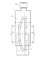
図1にMEMS型可変容量キャパシタ10の構造の一例を示す。
[Structure of MEMS Variable Capacitance Capacitor 10]
FIG. 1 shows an example of the structure of the
このMEMS型可変容量キャパシタ10は、基板(図示せず)に対し固定のアンカー部11から延びる可動部12と固定部13とを有し、可動部12に上部電極14を、固定部13に下部電極15を形成してなる。下部電極15の表面には、上部電極14との短絡を防ぐため、シリコン酸化膜等からなる絶縁膜16が形成されている。
This
上部電極14が形成される可動部12はアンカー部11(基板)に対し弾性力を持って可動に構成されている。このため、上部電極14は下部電極15に対し物理的に移動することが可能である。上部電極14と下部電極15とで構成されるキャパシタの静電容量Crfは、両電極間の距離dに応じて変化する。このキャパシタは、可変容量を必要とする回路に接続される。固定部13は梁部11に対して固定されている。
The
上部電極14、下部電極15は、電荷を保持するための主電極14a、15aに加え、主電極14a、15a間の距離を縮め又は維持するための補助電極14b、15bを備えている。補助電極14b、15b間に、距離dを縮めるための電圧(変形電圧Vact)を印加することで、クーロン力により主電極14a、15a間の距離dを縮めることができる。
The
逆に、補助電極14b、15bの間への電圧印加を止めると、可動部12は、元の位置に戻そうとする弾性力により、元の位置に戻る。したがって、主電極14a、15a間の距離dを縮めた後は、補助電極14b、15b間にある一定電圧(維持電圧Vhold)を印加し続けて、その距離dを一定に保つことで増加した容量Crfを維持することができる。
On the contrary, when the voltage application between the
また、この維持電圧Vholdは変形電圧Vactに比べて低い電圧となっている。主電極14a、15a間の静電引力は距離dの2乗に反比例するので、弾性力に抗して距離dを維持するため、変形電圧Vactほど高い電圧は必要ないからである。維持電圧Vholdを変形電圧Vactに比べて低い電圧にすることで、補助電極14b、15b間に挟まれる絶縁体16の中にトラップされる電荷量を小さくし、信頼性を高めている。このような補助電極14b、15bに印加する電圧をドライバIC20内の昇圧回路により生成する。
The sustain voltage Vhold is lower than the deformation voltage Vact. This is because the electrostatic attractive force between the
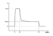
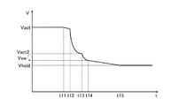
図2に、距離dを変化・維持させる場合において、ドライバIC20が生成し補助電極14b、15b間に供給する電圧の時間変化を示す。はじめに、時刻t1において、補助電極14b、15b間に、距離dを縮めるため、前述の変形電圧Vactを印加する。
FIG. 2 shows the time change of the voltage generated by the
その後、距離dを縮めた後、時刻t2において、これを一定に保つのに必要な電圧として、補助電極14b、15b間にVactよりも低い維持電圧Vholdを印加する。これにより、距離dが小さくなったことにより増加した容量Crfを高い状態に維持することができる。
Thereafter, after the distance d is shortened, at time t2, a sustain voltage Vhold lower than Vact is applied between the
その後、距離dの維持が不要になった場合、時刻t3において電圧を0Vに戻す。なお、MEMS型可変容量キャパシタ10の信頼性を維持する観点、及び消費電力を低減する観点から、変形電圧Vactを印加する時間は短いのが好ましく、例えば20μS以下が推奨される。
After that, when it becomes unnecessary to maintain the distance d, the voltage is returned to 0 V at time t3. From the viewpoint of maintaining the reliability of the MEMS
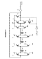
[ドライバIC20の全体構成]
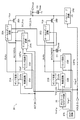
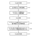
次に、ドライバIC20の具体的な構成を図3のブロック図を参照して説明する。このドライバIC20は、変形電圧Vactを生成・供給するための構成として、ポンプ回路21A、発振回路22A、リミッタ回路23A、ディスチャージ回路24A、ローカルポンプ回路25A及びnMOSトランジスタ26Aを備えている。
[Overall Configuration of Driver IC 20]
Next, a specific configuration of the
加えて、このドライバIC20は、維持電圧Vholdを生成・供給するための構成として、ポンプ回路21B、発振回路22B、リミッタ回路23B、ディスチャージ回路24B、ローカルポンプ回路25B及びnMOSトランジスタ26Bを備えている。
In addition, the
維持電圧Vholdは、変形電圧Vactに比べ印加時間が圧倒的に長い。このため、ポンプ回路22B、発振回路22B、リミッタ回路22B、ローカルポンプ回路25Bに関しては、低消費電力のものが用いられる。さらにこのドライバIC20は、リミッタ回路23A、23Bに対し基準電圧を供給するためのバンドギャップリファレンス回路27を有している。
The sustain voltage Vhold has an overwhelmingly longer application time than the deformation voltage Vact. For this reason, the
また、nMOSトランジスタ26AとnMOSトランジスタ26Bとは相補的に導通状態とされ、これにより、ポンプ回路21Aで生成された電圧、またはポンプ回路21Bで生成された電圧が選択的に出力端子OUTに供給されるようになっている。
In addition, the
このように、本実施の形態のICドライバ20では、変形電圧Vactを生成・供給するための回路群と、維持電圧Vholdを生成・供給するための回路群とが別々に設けられている。そして、MEMS型可変容量キャパシタ10の変形のため変形電圧Vactが印加されている間においては、nMOSトランジスタ26Aが導通し、nMOSトランジスタ26Bは非導通状態とされる。また、印加電圧を変形電圧Vactから維持電圧Vholdに変化させる場合、nMOSトランジスタ26Aは導通状態から非導通状態に切り替わり、代わりにnMOSトランジスタ26Bが非導通状態から導通状態に切り替わる。
As described above, in the
このように変形電圧Vactを生成・供給するための回路群と、維持電圧Vholdを生成・供給するための回路群とを別々に設けられ、トランジスタ26A、26Bのスイッチング動作が実行される構成をとることにより、低消費電力化を図ることができる。変形電圧Vactと、維持電圧holdとを1系統の回路群(1つのチャージポンプ回路、1つの発振器、1つのリミッタ回路)から供給する構成では、電圧の供給能力の向上と消費電力の低減とを両立することが難しい。すなわち、高電圧である変形電圧Vactを供給するためには、チャージポンプ回路の段数を多くする必要があるが、このような電圧Vactの生成のための多段チャージポンプ回路により維持電圧Vholdも生成することとすると、消費電力を低くすることができない。このため、本実施の形態では、変形電圧vactの供給回路群と、維持電圧Vholdの供給回路群とを別々に設け、スイッチング動作を行うことにより、電圧の供給能力の向上と消費電力の低減とを両立を図っているものである。
In this way, a circuit group for generating and supplying the deformed voltage Vact and a circuit group for generating and supplying the sustain voltage Vhold are separately provided, and the switching operation of the
このドライバIC20は、上記の各回路ブロックが以下に詳細に説明するように構成されていることにより、変形電圧Vact及び維持電圧Vholdを、電源電圧の変動、周囲温度の変化及び製造プロセスのバラツキに拘わらず略一定とすることを可能としている。
The
ただし、この図3のような構成の場合、nMOSトランジスタ26A及びnMOSトランジスタ26Bのドレイン−ソース間電圧が大きく変化し、nMOSトランジスタ26A、26Bの経年変化による信頼性の問題が生じる虞がある。後述の説明から明らかとなるように、本実施の形態では、MEMS型可変容量キャパシタ10に印加する電圧を変形電圧Vactから維持電圧Vholdに切り換える場合において、トランジスタ26A、26Bの劣化および信頼性の問題が生じることを回避している。
However, in the case of the configuration shown in FIG. 3, the drain-source voltages of the
ポンプ回路21Aは、制御信号ACT_Enに従って、発振回路22Aから供給されるクロック信号CLKaの立ち上がり毎に電源電圧を昇圧させ、昇圧電圧を出力ノードACTNODEに出力する動作を行う。リミッタ回路23Aは、バンドギャップリファレンス回路27から与えられる基準電圧Vbgr1に基づき、出力ノードACTNODEの出力電圧が所定の上限値を超えたか否かを検出し、この上限値を超えた場合にリミッタ信号LMTaを出力して発振回路22Aの動作を停止させる。ディスチャージ回路24Aは、制御信号ACT_Enが”L”に変化してから所定時間経過後に出力ノードACTNODEをディスチャージする動作を開始するように構成されている。
In accordance with the control signal ACT_En, the
ローカルポンプ回路25Aは、出力ノードACTNODEの電圧を、クロック信号CLKaに従って更に昇圧させる。nMOSトランジスタ26Aは、ゲート電圧Vgaにより導通し、出力ノードACTNODEの電圧を出力ノードOUTに転送する機能を有する。ここで、ゲート電圧Vgaは、転送すべき出力ノードACTNODEの電圧Vactよりも、トランジスタ26Aの閾値電圧の分だけ高い電圧である。なお、出力ノードOUTと接地電位との間には、電位安定化のためキャパシタC2(容量値Cload)が設けられている。
The
ポンプ回路21Bは、制御信号HOLD_Enに従って、発振回路22Bから供給されるクロック信号CLKbの立ち上がり毎に、電源電圧を昇圧させて昇圧電圧を出力ノードHOLDNODEに出力する動作を行う。発振回路22Bは、バンドギャップリファレンス回路27からボルテージフォロワ回路28を介して供給される電圧Vref_oscに基づき前述のクロック信号CLKbを供給する。このクロック信号CLKbは、クロック信号CLKaよりも小さい周波数で構わない。これは、維持電圧Vholdは、変形電圧Vactに比べ小さいためである。
The
リミッタ回路23Bは、バンドギャップリファレンス回路27から与えられる基準電圧Vbgr2に基づき、ポンプ回路21Bの出力ノードHOLDNODEの出力電圧が所定の上限値を超えたか否かを検出し、この上限値を超えた場合にリミッタ信号LMTbを出力して発振回路22Bの動作を停止させる。なお、出力ノードHOLDNODEと接地電位との間には、電位安定化のためのキャパシタC1(容量値Chold)が設けられている。ディスチャージ回路24Bは、維持電圧Vholdの印加動作の終了後、出力端子OUTに接続されたキャパシタC2の電荷を引き抜いて出力端子OUTの電圧を0Vに戻す動作を行う。
The
ローカルポンプ回路25Bは、出力ノードHOLDNODEの電圧を、クロック信号CLKbに従って更に昇圧させる。なお、ローカルポンプ回路25Bは、ローカルポンプ回路25Aからのイネーブル信号DC_Enbを受けて動作を開始するように構成されている。nMOSトランジスタ26Bは、ゲート電圧Vgbにより導通し、出力ノードHOLDNODEの電圧を出力ノードOUTに転送する機能を有する。ここで、ゲート電圧Vgbは、転送すべき出力ノードHOLDNODEの電圧Vholdよりも、トランジスタ26Bの閾値電圧の分だけ高い電圧である。バンドギャップリファレンス回路27は、温度に依存せず電源電圧に依存しない基準電圧Vref_pおよびVref_nを出力する。ボルテージフォロワ回路28は、この基準電圧Vref_p及びVref_nを入力して出力電圧Vref_oscを出力する回路である。
The
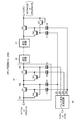
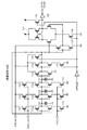
[ポンプ回路21A、21B]
図4は、ポンプ回路21A、21Bの具体的構成を示す回路図である。図4に示すように、ポンプ回路21A、21Bは、複数段(図4では3段)の昇圧回路31、32、33、及びパルス波形生成回路34を備えている。昇圧回路31、32、33はそれぞれ、nMOSトランジスタQ1〜Q4、及びキャパシタC3〜C6を備えている。
[
FIG. 4 is a circuit diagram showing a specific configuration of the
nMOSトランジスタQ1は、制御信号ACT_En又はHOLD_Enの入力端子であるノードN1とノードN2との間に電流経路を有するように接続され、転送トランジスタとして機能する。nMOSトランジスタQ2は、ノードN1とnMOSトランジスタQ1のゲートとの間に電流経路を有するように接続され、そのゲートはノードN2に接続されている。このnMOSトランジスタQ2は、トランジスタQ1のゲートを昇圧するためのプリチャージ用トランジスタとして機能するものである。 The nMOS transistor Q1 is connected so as to have a current path between the node N1 and the node N2, which are input terminals of the control signal ACT_En or HOLD_En, and functions as a transfer transistor. The nMOS transistor Q2 is connected so as to have a current path between the node N1 and the gate of the nMOS transistor Q1, and the gate thereof is connected to the node N2. The nMOS transistor Q2 functions as a precharging transistor for boosting the gate of the transistor Q1.
nMOSトランジスタQ3は、ノードN2とノードN3との間に電流経路を有するように接続され、転送トランジスタとして機能する。nMOSトランジスタQ4は、ノードN2とnMOSトランジスタQ3のゲートとの間に電流経路を有するように接続され、そのゲートはノードN3に接続されている。このnMOSトランジスタQ4は、トランジスタQ3のゲートを昇圧するためのプリチャージ用トランジスタとして機能するものである。 The nMOS transistor Q3 is connected so as to have a current path between the node N2 and the node N3, and functions as a transfer transistor. The nMOS transistor Q4 is connected to have a current path between the node N2 and the gate of the nMOS transistor Q3, and the gate is connected to the node N3. The nMOS transistor Q4 functions as a precharging transistor for boosting the gate of the transistor Q3.
また、キャパシタC3、C5はそれぞれnMOSトランジスタQ1、Q3のゲートにその一端が接続され、キャパシタC4、C6はそれぞれノードN2、N3にその一端が接続されている。トランジスタC3〜C6の他端は、パルス生成回路34からパルス信号B1〜B4を供給される。パルス信号B1〜B4は、位相が90度ずつ異なる4相信号である。
Capacitors C3 and C5 have their one ends connected to the gates of nMOS transistors Q1 and Q3, respectively, and capacitors C4 and C6 have their one ends connected to nodes N2 and N3, respectively. The other ends of the transistors C3 to C6 are supplied with pulse signals B1 to B4 from the
なお、昇圧回路33の後段に形成されるnMOSトランジスタQ5、Q6、及びキャパシタC7、C8も昇圧回路を構成する。nMOSトランジスタQ5は、昇圧回路33の出力端子と出力ノードOUT21(出力ノードACTNODEまたはHOLDNODE)の間に電流経路を有するように接続され、一方、nMOSトランジスタQ6は、昇圧回路33の出力端子とnMOSトランジスタQ5のゲートとの間に電流経路を有するように接続されている。また、キャパシタC7、C8はそれぞれnMOSトランジスタQ6、Q5のゲートにその一端が接続されている。トランジスタC7、C8の他端は、パルス生成回路34からパルス信号B1、B4を供給される。また、出力ノードOUT21とnMOSトランジスタQ6のゲートとの間には、ダイオード接続されたnMOSトランジスタQ7が接続されている。このnMOSトランジスタQ7は、nMOSトランジスタQ6のゲートをプリチャージするためのプリチャージ用トランジスタとして機能する。
The nMOS transistors Q5 and Q6 and the capacitors C7 and C8 formed at the subsequent stage of the booster circuit 33 also constitute a booster circuit. The nMOS transistor Q5 is connected to have a current path between the output terminal of the booster circuit 33 and the output node OUT21 (output node ACTNODE or HOLDNODE), while the nMOS transistor Q6 is connected to the output terminal of the booster circuit 33 and the nMOS transistor. A current path is connected to the gate of Q5. Capacitors C7 and C8 have one ends connected to the gates of nMOS transistors Q6 and Q5, respectively. The other ends of the transistors C7 and C8 are supplied with pulse signals B1 and B4 from the
なお、維持電圧Vholdは変形電圧Vactよりも小さく、しかも維持電圧Vholdの印加時にはキャパシタC2は充電済みであるため、ポンプ回路21Bに含まれる昇圧回路の段数は、ポンプ回路21Aに含まれる昇圧回路の段数よりも少なくすることができる。
Since sustain voltage Vhold is smaller than deformation voltage Vact and capacitor C2 is charged when sustain voltage Vhold is applied, the number of stages of the booster circuit included in
[発振回路22A]
次に、発振回路22Aの具体的な構成を図5を参照して説明する。この発振回路22Aは、複数のCMOSインバータ41をリング状(閉ループ状)に接続したリングオシレータである。CMOSインバータ41の間には、電荷保持用のキャパシタ42(容量値C)が接続され、キャパシタ42の一端は接地されている。また、各CMOSインバータ41を構成するpMOSトランジスタとnMOSトランジスタの間には抵抗46(抵抗値R)が接続される。この抵抗値Rと、容量値Cにより決まる遅延量により、発振回路22Aが出力するクロック信号CLKaの周波数が決定される。
[
Next, a specific configuration of the
最後尾のインバータ41中の出力端子と電源端子との間には、pMOSトランジスタ43が接続される。また、最後尾のインバータ41中のnMOSトランジスタのソースと接地端子との間には、nMOSトランジスタ44が接続されている。両トランジスタ43、44のゲートには、インバータ45を介してリミッタ信号LMTa又はLMTbが入力される。リミッタ信号LMTa、LMTbは、リミッタ回路23A、23Bから出力される。このPMOSトランジスタ43、nMOSトランジスタ44が導通することにより、発振回路22Aは発振動作を停止する。
A
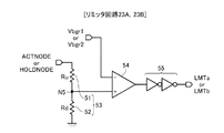
[リミッタ回路23A、23B]
次に、リミッタ回路23A、23Bの具体的構成を図6を参照して説明する。このリミッタ回路23A、23Bは、同一の構成を有し、それぞれ抵抗51(抵抗値Ru)、52(抵抗値Rd)を接続ノードN5にて直列接続してなる分割抵抗53、差動増幅器54、及びインバータ55を備えている。
[
Next, a specific configuration of the
抵抗51の一端はポンプ回路21A又は21Bの出力端子OUT(ノードACTNODE、HOLDNODE)に接続されている。また、抵抗52の一端は接地端子に接続されている。
One end of the
差動増幅器54は、反転入力端子にバンドギャップリファレンス回路27で発生させた参照電位Vbgr1又はVbgr2を、非反転入力端子に接続ノードN5の電圧を供給されている。この差動増幅器54の出力信号がインバータ55に入力される。インバータ55の出力信号が、前述したリミッタ信号LMTである。すなわち、分割抵抗53の接続ノードN5の電圧が参照電位Vbgr1またはVbgr2以上となった場合に、リミッタ信号LMTが”L”から”H”に立ち上がり、発振回路22Aの動作が停止される。なお、リミッタ回路23Aと23Bとでは、分割抵抗53の分割抵抗比が異なっており、後者のそれは前者のそれよりも小さくされている。
In the
また、分割抵抗53の抵抗値(Ru+Rd)を大きくすることにより、リミッタ回路23A、23Bを流れるバイアス電流を小さくすることができる。しかし、バイアス電流を小さくした場合、リミッタ回路23A、23Bの反応速度が遅くなり、このため、出力ノードACTNODE、HOLDNODEの電圧のリプルが大きくなる。ただしこの場合でも、キャパシタC1の容量Choldを大きくすることにより、リプルを抑えることができる。
Also, by increasing the resistance value (Ru + Rd) of the dividing
[ディスチャージ回路24A]
次に、ディスチャージ回路24Aの具体的構成を図7を参照して説明する。このディスチャージ回路24Aは、前述のように、ディスチャージ回路24Aは、制御信号ACT_Enが”L”に変化してから所定時間経過後に出力ノードACTNODEをディスチャージする動作を開始するように構成されている。
[
Next, a specific configuration of the
このディスチャージ回路24Aは、インバータ60、ANDゲート61、インバータ62、フリップフロップ63、インバータ64、及びフリップフロップ65を有する。インバータ60の入力端子には、制御信号ACT_Enが入力され、その出力端子はANDゲート61の1つの入力端子に接続される。ANDゲート61の他方の入力端子には、クロック信号CLKaが入力される。ANDゲート61の出力端子は、フリップフロップ63の1つの入力端子に接続されている。
The
インバータ62の入力端子はフリップフロップ63の出力端子と接続され、その出力端子はフリップフロップ63のもう1つの入力端子に接続されている。インバータ64とフリップフロップ65も同様に接続されている。フリップフロップ63の出力端子は、フリップフロップ65の入力端子に接続されている。制御信号ACT_Enは、フリップフロップ63、65のリセット端子にも供給される。これにより、インバータ62、64及びフリップフロップ63、65は、制御信号ACT_Enの立ち上がり後、クロック信号CLKaよりも所定時間遅延した信号をインバータ70に出力する。
The input terminal of the
また、フリップフロップ63、65の出力端子は、それぞれインバータ67、70を介してラッチ回路68、71の1つの入力端子に接続されている。
The output terminals of the flip-
ラッチ回路68のもう1つの入力端子は、インバータ66により制御信号ACT_Enの反転信号/ACT_Enを供給されている。また、ラッチ回路71のもう1つの入力端子も同様に、インバータ66により制御信号ACT_Enの反転信号/ACT_Enを供給されている。ラッチ回路68、71の出力信号の反転信号は、それぞれインバータ69、72を介してトランジスタQ14、Q16に供給されている。
The other input terminal of the
出力ノードACTNODEと接地端子との間には、nMOSトランジスタQ11〜Q14が直列接続されると共に、nMOSトランジスタQ15、Q16が直列接続されている。nMOSトランジスタQ11、Q12はダイオード接続されており、nMOSトランジスタQ13、Q15は所定の電源電圧をゲートに供給されている。ラッチ回路68、71の状態に応じて、nMOSトランジスタQ14、Q16が導通し、出力ノードACTNODEが放電される。nMOSトランジスタQ14はQ16よりも先に導通し、出力ノードACTNODEを所定の電位まで放電する。次いで、nMOSトランジスタQ16が導通し、出力ノードACTNODEを接地電位まで放電する。
Between the output node ACTNODE and the ground terminal, nMOS transistors Q11 to Q14 are connected in series, and nMOS transistors Q15 and Q16 are connected in series. The nMOS transistors Q11 and Q12 are diode-connected, and the nMOS transistors Q13 and Q15 are supplied with a predetermined power supply voltage at their gates. Depending on the state of
また、前述のリミッタ信号LMTaは、インバータ73に入力される。インバータ73の出力端子は、ANDゲート74の1つの入力端子に接続される。また、ANDゲート74の他方の入力端子には、ラッチ回路68の出力信号の反転信号がインバータ69から入力される。ANDゲート74の出力端子は、インバータ75に入力され、インバータ75の出力端子はラッチ回路76の1つの入力端子に接続される。ラッチ回路76の出力信号は、2つのインバータ77、78を介して、出力信号DC_Enaとしてローカルポンプ回路25Aに出力される。
Further, the aforementioned limiter signal LMTa is input to the
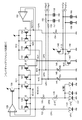
[ローカルポンプ回路25A]
次に、ローカルポンプ回路25Aの具体的構成を図8を参照して説明する。図8のローカルポンプ回路25Aは、出力ノードACTNODEの電圧を昇圧して、nMOSトランジスタ26Aのゲートに入力するゲート電圧Vgaを生成し、もpってnMOSトランジスタ26Aの導通を制御するためのチャージポンプ回路である。また、このローカルポンプ回路25Aは、ディスチャージ回路24Aからの出力信号DC_Ena=”L”の入力後、出力ノードACTNODEの電圧を昇圧して昇圧電圧Vgaを生成する動作を停止すると共に、所定時間経過後に出力端子OUTLPaをディスチャージするように構成されている。出力端子OUTLPaをディスチャージするタイミングは、ディスチャージ回路24Aにより出力ノードACTNODEがディスチャージするタイミングよりも遅くされている。これにより、nMOSトランジスタ26Aのドレイン−ソース間に高電圧が印加されることを防止し、nMOSトランジスタ26Aの特性劣化を防止している。
[
Next, a specific configuration of the
すなわち、ローカルポンプ回路25Aは、出力ノードACTNODEと出力端子OUTLPaとの間に直列接続されたnMOSトランジスタQ21〜Q24を備えている。これらのnMOSトランジスタQ21〜Q24は出力ノードACTNODE側から出力端子OUTLPaに向かう方向が順方向となるようにダイオード接続されており、そのゲートには、キャパシタC21〜C24が接続されている。また、出力ノードACTNODEと出力端子OUTLPaとの間には、nMOSトランジスタQ25、Q26が、出力端子OUTLPaから出力ノードACTNODEに向かう方向が順方向となるようにダイオード接続されている。
That is, the
また、クロック信号CLKaに基づく信号をキャパシタC21〜C24の他端に入力しチャージポンプ動作を行うための構成として、NANDゲート81、インバータ82、83が設けられている。NANDゲート81の1つの入力端子にはクロック信号CLKaが入力され、他方の入力端子にはディスチャージ回路24Aからの出力信号である出力信号DC_Enaが入力される。
Further, a
インバータ82の入力端子には、NANDゲート81の出力端子が接続されている。インバータ82の出力端子は、キャパシタC22、C24の他端に接続されている。また、インバータ83の入力端子は、インバータ82の出力端子に接続されており、インバータ83の出力端子は、キャパシタC21、キャパシタC23の他端に接続されている。
The output terminal of the
クロック信号CLKaが入力されることにより、出力ノードACTNODEの電圧がトランジスタQ21〜Q24を介して転送され、出力端子OUTLPaの電圧Vgaが昇圧される。出力端子OUTLPaの電圧Vgaが高くなりすぎた場合には、電荷がトランジスタQ26,Q25を介して出力ノードACTNODEに戻されて、出力端子OUTLPaの電圧Vgaが下げられる。 When the clock signal CLKa is input, the voltage of the output node ACTNODE is transferred through the transistors Q21 to Q24, and the voltage Vga of the output terminal OUTLPa is boosted. If the voltage Vga at the output terminal OUTLPa becomes too high, the charge is returned to the output node ACTNODE via the transistors Q26 and Q25, and the voltage Vga at the output terminal OUTLPa is lowered.
また、このローカルポンプ回路25Aは、インバータ84、ANDゲート85、インバータ86、フリップフロップ87、インバータ88、フリップフロップ89、インバータ90、及びフリップフロップ91を有する。
The
インバータ84の入力端子には、出力信号DC_Enaが入力され、その出力端子はANDゲート85の1つの入力端子に接続される。ANDゲート85の他方の入力端子には、クロック信号CLKaが入力される。ANDゲート85の出力端子は、フリップフロップ87の1つの入力端子に接続されている。
An output signal DC_Ena is input to the input terminal of the
インバータ86の入力端子はフリップフロップ87の出力端子と接続され、その出力端子はフリップフロップ87のもう1つの入力端子に接続されている。インバータ88とフリップフロップ89も同様に接続されており、また、インバータ90とフリップフロップ91も同様に接続されている。フリップフロップ87の出力端子は、フリップフロップ89の入力端子に接続されている。フリップフロップ89の出力端子は、フリップフロップ91の入力端子に接続されている。また、出力信号DC_Enaは、フリップフロップ87、89、91のリセット端子にも供給される。これにより、インバータ86,88,90及びフリップフロップ87,89,91は、出力信号DC_Enaの立ち上がり後、クロック信号CLKaよりも所定時間遅延した信号をインバータ105に出力する。
The input terminal of the
また、フリップフロップ87、89の出力端子は、それぞれインバータ93、96を介してラッチ回路94、97の1つの入力端子に接続されている。ラッチ回路94、97のもう1つの入力端子は、インバータ92により制御信号DC_Enaの反転信号/DC_Enaを供給されている。ラッチ回路94,97の出力信号の反転信号は、インバータ95,98を介してトランジスタQ24、Q26に供給されている。
The output terminals of the flip-
出力端子OUTLPaと接地端子との間には、nMOSトランジスタQ31〜Q34が直列接続されると共に、nMOSトランジスタQ35、Q36が直列接続されている。nMOSトランジスタQ31、Q32はダイオード接続されており、nMOSトランジスタQ33、Q35は所定の電源電圧をゲートに供給されている。ラッチ回路93,96の状態に応じて、nMOSトランジスタQ34、Q36が導通し、出力端子OUTLPaが放電される。
Between the output terminal OUTLPa and the ground terminal, nMOS transistors Q31 to Q34 are connected in series, and nMOS transistors Q35 and Q36 are connected in series. The nMOS transistors Q31 and Q32 are diode-connected, and the nMOS transistors Q33 and Q35 are supplied with a predetermined power supply voltage at their gates. Depending on the states of the
nMOSトランジスタQ34はnMOSトランジスタQ36よりも先に導通し、nMOSトランジスタQ36はnMOSトランジスタQ34よりも遅れて導通する。nMOSトランジスタQ34が導通した場合、ダイオード接続されたnMOSトランジスタQ31、nMOSトランジスタQ32の存在のため、出力端子OUTLPaの電圧は、ダイオードの順方向電圧の2倍程度まで低下する。続いてnMOSトランジスタQ36が導通すると、出力端子OUTLPaの電圧は接地電位まで低下する。 The nMOS transistor Q34 conducts before the nMOS transistor Q36, and the nMOS transistor Q36 conducts later than the nMOS transistor Q34. When the nMOS transistor Q34 is turned on, the voltage at the output terminal OUTLPa drops to about twice the forward voltage of the diode because of the presence of the diode-connected nMOS transistor Q31 and nMOS transistor Q32. Subsequently, when the nMOS transistor Q36 is turned on, the voltage at the output terminal OUTLPa drops to the ground potential.
また、インバータ105の出力信号、及び出力信号DC_Enaの反転信号を入力端子に供給されるラッチ回路106と、このラッチ回路106の出力信号を反転するインバータ107とが設けられている。インバータ107の出力信号は、出力信号DC_Enbとして、後述するローカルポンプ回路25Bに供給される。
Further, a
[発振回路22B]
次に、発振回路22Bの具体的構成を図9を参照して説明する。図9の発振回路22Bは、図5の発振回路22Aと同様に、複数のCMOSインバータ111(a〜e)がリング状に形成されたリングオシレータである。また、複数のCMOSインバータ111a〜111dの間のノードには、接地端子との間にキャパシタ114が接続されている。
[
Next, a specific configuration of the
ただし、この実施の形態では、各CMOSインバータ111が図5のような抵抗46を有しておらず、代わりに定電流源からカレントミラー回路を用いて定電流を流す定電流回路を備えており、また、バンドギャップリファレンス回路27から供給された定電圧に基づいてボルテージフォロワ回路28で生成された電圧Vref_osc、及びVref_p_oscにより駆動されている。これにより、遅延時間が電源電圧、温度、及びプロセス等に依存し難い発振回路となっており、電圧Vholdの安定性が担保されている。複数のインバータ111の一部(図9Aでは、前段の3つのインバータ111a〜c)は、その一端にpMOSトランジスタ112を接続されている一方、その他端にnMOSトランジスタ113を接続されている。pMOSトランジスタ112のソースは、ボルテージフォロワ回路28から供給された電圧Vref_oscを共通に与えられており、nMOSトランジスタ113のソースはいずれも接地されている。
However, in this embodiment, each CMOS inverter 111 does not have the
また、pMOSトランジスタ112のゲートには、ボルテージフォロワ回路28から供給される電圧Vref_p_oscが供給され、nMOSトランジスタ113のゲートには電圧Vref_nが供給されている。
Further, the voltage Vref_p_osc supplied from the
また、4段目のCMOSインバータ111dは、pMOSトランジスタ112を有さず直接電圧Vref_oscを供給され、他端は接地されている。また、最後尾のCMOSインバータ111eも、直接Vref_oscを供給され、他端はnMOSトランジスタ115のドレインに接続されている。nMOSトランジスタ115のソースは接地されている。また、インバータ111eの出力端子と電圧Vref_oscの出力端子との間には、pMOSトランジスタ116が接続されている。
The fourth-
nMOSトランジスタ115のゲート及びpMOSトランジスタ116のゲートは、リミッタ信号LMTbの反転信号を供給されている。すなわち、この発振回路22bは、出力ノードHOLDNODEの電圧が上限値を超えた場合に、その発振動作を停止するように構成されている。
The gate of the
また、この最後尾のCMOSインバータ111eには、レベルシフタ117が接続されている。このレベルシフタ119の出力端子にはインバータ120が接続されており、このインバータ120の出力信号がクロック信号CLKbとして出力される。なお、pMOSトランジスタ119は、リミッタ信号LMTbに基づいて、レベルシフタ119の出力端子を電源電位に固定するためのpMOSトランジスタである。また、インバータ111fは、最後尾のCMOSインバータ111eの出力信号の反転信号を生成して、レベルシフタ119の1つの入力端子に供給するものである。
A
[ローカルポンプ回路25B]
次に、ローカルポンプ回路25Bの具体的構成を図10を参照して説明する。図10のローカルポンプ回路25Bは、ローカルポンプ回路25Aからの出力信号DC_Enbの立ち上がり後、出力ノードHOLDNODEの電圧を昇圧して昇圧電圧VGbを出力端子OUTLPbから出力するチャージポンプ回路である。具体的な構成は、フリップフロップ回路91、インバータ105,107及びラッチ回路106を備えていない点においてローカルポンプ回路25Aと異なり、その他は同一である。図10において、図8と同一の構成要素については同一の符号を付しているので、これらについての詳細な説明は省略する。
[
Next, a specific configuration of the
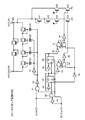
[バンドギャップリファレンス回路27]
次に、バンドギャップリファレンス回路27の具体的構成を、図11を参照して説明する。バンドギャップリファレンス回路27は、上述のように、電源電圧、周囲温度及びプロセス等に依存しない出力電圧Vbgr1、Vbgr2を出力するように設計されているものである。このバンドギャップリファレンス回路27は、ノードN11とノードN12を有し、これらノードN11又はN12と接地端子との間に複数の電流経路CP1〜CP6を有している。
[Band Gap Reference Circuit 27]
Next, a specific configuration of the band gap reference circuit 27 will be described with reference to FIG. As described above, the band gap reference circuit 27 is designed to output the output voltages Vbgr1 and Vbgr2 independent of the power supply voltage, the ambient temperature, the process, and the like. The band gap reference circuit 27 has a node N11 and a node N12, and a plurality of current paths CP1 to CP6 between the node N11 or N12 and the ground terminal.
まず、第1の電流経路CP1は、pMOSトランジスタ131、抵抗132(抵抗値R6)、及びダイオード133(順方向電圧VF1)が直列接続されて形成される。
First, the first current path CP1 is formed by connecting a
pMOSトランジスタ131のゲート(ノードN13)は、差動増幅器138の非反転入力端子に接続され、ドレイン(ノードN14)は差動増幅器139の反転入力端子に接続されている。
The gate (node N13) of the
差動増幅器138の出力端子はpMOSトランジスタ139のゲートに接続されている。pMOSトランジスタ139のソースは電源電圧を供給され、ドレインはノードN11に接続されている。差動増幅器138はノードN13、N14の電圧が等しくなるようにpMOSトランジスタ139のゲート電圧を制御する。なお、pMOSトランジスタ131に流れる電流をI1と定義し、ダイオード133の順方向電圧をVF1と定義する。
The output terminal of the
また、第2の電流経路CP2は、pMOSトランジスタ134、抵抗135(抵抗値R7)、抵抗136(抵抗値R1)、及び並列接続ダイオード137(N個:順方向電圧VF2)が直列接続されて形成される。
The second current path CP2 is formed by connecting a
pMOSトランジスタ134のドレイン及びゲートはノードN13に接続され、これによりpMOSトランジスタ134はpMOSトランジスタ131と共にカレントミラー回路を構成している。なお、pMOSトランジスタ134に流れる電流をI2と定義すると共に、ダイオード137の順方向電圧をVF2と定義する。
The drain and gate of the
また、ダイオード133の順方向電圧VF1とダイオード1137の順方向電圧VF2との差に基づき抵抗136に印加される電圧をΔVF(=VF1−VF2)と定義する。
A voltage applied to the
なお、抵抗132と135が存在することにより、差動増幅器138に入力される電圧の大きさを高くすることができ、これにより、差動増幅器138内のトランジスタを飽和領域で動作させることができ、電圧変動に対するゲインを低減することができる。抵抗132と135のマッチングばらつきの影響が生じるが、ノードN14に対するノイズの増幅機能を抑制することもできる。このため、抵抗132、135を形成することにより、全体としてバンドギャップリファレンス回路27の出力電圧Vbgr1のバラツキを低減することができる。
Note that the presence of the
また、第3の電流経路CP3は、pMOSトランジスタ140、151及び可変抵抗144(抵抗値R2a)により形成されている。pMOSトランジスタ140はノードN11とノードN15の間に電流経路を有するよう接続され、ゲートはノードN13に接続されている。これにより、pMOSトランジスタ140は、pMOSトランジスタ131及び134と共にカレントミラー回路を構成している。なお、このpMOSトランジスタ140に流れる電流をI3と定義する。
The third current path CP3 is formed by the
一方、pMOSトランジスタ151はノードN12とノードN15の間に電流経路を有するよう接続され、ゲートはノードN20に接続されている。このpMOSトランジスタ151に流れる電流をI4と定義する。
On the other hand, the
また、抵抗144の抵抗値R2aは、出力ノードACTNODEの電圧が変形電圧Vactに達した後のある時点において、図示しない制御回路により、第1の値R2a1からこれよりも小さい第2の値R2a2(<R2a1)に切り換えられる。これにより、バンドギャップリファレンス回路27が出力する電圧Vbgr1が、抵抗144の抵抗値の変更前と比較して小さい値に変更される。なお、ノードN15と接地端子との間には抵抗155を介してキャパシタ157が接続されている。
Further, the resistance value R2a of the resistor 144 is changed from a first value R2a1 to a second value R2a2 (which is smaller than this) by a control circuit (not shown) at a certain point after the voltage of the output node ACTNODE reaches the deformed voltage Vact. <R2a1). As a result, the voltage Vbgr1 output from the band gap reference circuit 27 is changed to a smaller value than before the resistance value of the resistor 144 is changed. A
ノードN13は差動増幅器138の非反転入力端子に接続されている。また、pMOSトランジスタ151のゲートはノードN20に接続されている。ノードN20は、差動増幅器153の出力端子にも接続されている。可変抵抗144はノードN15と接地端子との間に接続されている。
Node N13 is connected to the non-inverting input terminal of
また、第4の電流経路CP4は、pMOSトランジスタ141、pMOSトランジスタ150及び可変抵抗145(抵抗値R2b)により形成されている。pMOSトランジスタ141はノードN11とノードN16の間に電流経路を有するよう接続され、pMOSトランジスタ150はノードN12とノードN16の間に電流経路を有するよう接続されている。
The fourth current path CP4 is formed by a
また、pMOSトランジスタ141のゲートはノードN13に接続され、pMOSトランジスタ150のゲートはノードN20に接続されている。従って、pOSトランジスタ141は、pMOSトランジスタ131,134、140と共にカレントミラー回路を構成し、pMOSトランジスタ150は、pMOSトランジスタ151と共にカレントミラー回路を構成する。
The gate of the
また、可変抵抗145はノードN16と接地端子との間に接続されている。なお、ノードN16と接地端子との間には抵抗155を介してキャパシタ158が接続されている。
The variable resistor 145 is connected between the node N16 and the ground terminal. A
更に、第5の電流経路CP5は、pMOSトランジスタ142、143、抵抗46及びnMOSトランジスタ147により形成されている。pMOSトランジスタ142はノードN11とノードN17の間に電流経路を有するように接続され、pMOSトランジスタ131、134、140、141と同様に、ゲートにノードN13が接続され、これらと共にカレントミラー回路を構成している。
Further, the fifth current path CP5 is formed by the
pMOSトランジスタ143はノードN12とN17の間に電流経路を有するよう接続され、そのゲートはノードN20に接続され、pMOSトランジスタ151、152と共にカレントミラー回路を構成している。
The
抵抗146とnMOSトランジスタ147とは、ノードN17と接地端子との間に直列接続されている。nMOSトランジスタ147はダイオード接続されている。また、ダイオード接続されたpMOSトランジスタ148とnMOSトランジスタ149とが電源電圧端子と接地端子との間において直列接続されている。
The
nMOSトランジスタ149のゲート(ノードN18)は、nMOSトランジスタ147のゲート及びドレインと接続されている。ノードN18、及びN19には、電圧Vref_p、Vref_nを出力するための端子が接続されている。なお、ノードN18、ノードN19と接地端子との間には、キャパシタ159、160が接続されている。
The gate (node N18) of the
また、pMOSトランジスタ152と、これに直列接続された抵抗154(抵抗値RX)により、第6の電流経路CP6が形成されている。pMOSトランジスタ152は、ノードN12とノードN21の間に電流経路を有するように接続されている。また、pMOSトランジスタ152は、pMOSトランジスタ150、151と同様に、そのゲートがノードN20に接続され、これらのトランジスタと共にカレントミラー回路を構成している。
The sixth current path CP6 is formed by the
なお、ノードN21は、差動増幅器153の非反転入力端子に接続されている。差動増幅器153の反転入力端子は、ノードN14に接続されている。差動増幅器153は、ノードN21の電圧VCがノードN14の電圧VAと等しくなるよう、ノードN20の電圧を制御する。
The node N21 is connected to the non-inverting input terminal of the
ここで、図11に示すバンドギャップリファレンス回路27の動作について説明する。 Here, the operation of the band gap reference circuit 27 shown in FIG. 11 will be described.
1つのダイオード133にかかる電圧をVF1、N個並列接続されたダイオード137にかかる電圧をVF2とした場合、電流経路CP1とCP2を流れる電流I1と12の間には、次の式が成り立つ。
When the voltage applied to one

ここで、Isはダイオードの逆方向飽和電流、VT=kT/q、VF1及びVF2はダイオード133、137の順方向電圧を示している。I1とI2、nMOSトランジスタ131、134のサイズにより決まり、両者が同一のサイズであればI1=I2となる。抵抗132,135の抵抗値を各々R6、R7と定義した場合、R6*I1=R7*I2の関係が成り立つような設計がなされる。
Here, Is is the reverse saturation current of the diode, VT = kT / q, VF1 and VF2 are the forward voltages of the
差動増幅器138は、ノードN13の電位とノードN14の電位が等しくなるようにその出力電圧を制御し、電流I1、I2の大きさを制御する。また、抵抗136には、電圧VF1とVF2の差であるΔVF(=VF1−VF2)が印加される。電圧ΔVFは、以下の数式により表現される。
The
ここで、バンドギャップリファレンス回路27の出力電圧Vbgr1を生成する電流の一部である電流I3をI1=I3の関係式が成り立つように設計すると(トランジスタ131と140を同一のサイズとして)、電流I3は、次の数式により表現される。
Here, when the current I3 that is a part of the current that generates the output voltage Vbgr1 of the bandgap reference circuit 27 is designed so that the relational expression of I1 = I3 holds (with the
一方、出力電圧Vbgr1を生成する電流の一部である電流I4についても、I4=I5の関係式が成り立つように設計する。ノードN14の電圧VAは、次の数式で表現され得る。 On the other hand, the current I4 that is a part of the current that generates the output voltage Vbgr1 is also designed so that the relational expression of I4 = I5 holds. The voltage VA of the node N14 can be expressed by the following formula.
また、ノードN21の電圧をVCとした場合、
VA=VCであるから、電流I4は、次の式で表現される。
Further, when the voltage of the node N21 is VC,
Since VA = VC, the current I4 is expressed by the following equation.
出力電圧Vbgr1は、電流I3のI4の和の電流が流れ込む抵抗144により生成され、次の式で表現される。 The output voltage Vbgr1 is generated by a resistor 144 into which a current that is the sum of I4 of current I3 flows, and is expressed by the following equation.
となる。また、出力電圧Vbgr1の温度係数が0となる条件は、
であり、この時、出力電圧Vbgr1は、次式により表現される。 At this time, the output voltage Vbgr1 is expressed by the following equation.
このように図11のバンドギャップリファレンス回路27の出力電圧Vbgr1は、温度依存性を有さず、且つ可変抵抗144の抵抗値R2aを制御することにより、その値を変更することができる。この出力電圧Vbgr1が、ドライバIC20からの出力電圧を変形電圧Vactから維持電圧Vholdに切り換える段階において、出力電圧Vbgr1を低い電圧値に切り替えることにより、トランジスタ26A及び26Bに与える負荷を小さくすることができる。
As described above, the output voltage Vbgr1 of the band gap reference circuit 27 of FIG. 11 does not have temperature dependence, and can be changed by controlling the resistance value R2a of the variable resistor 144. When the output voltage Vbgr1 switches the output voltage from the
また、このバンドギャップリファレンス回路27では、出力電圧Vbgr1を、出力段の電流経路CP3においてダイオードを使用することなく出力している。また、抵抗も可変抵抗144の1つのみである。このため、ダイオードの特性バラツキや抵抗のマッチング特性のバラツキ等により出力電圧Vbgr1が変動することを抑制することができる。 In the band gap reference circuit 27, the output voltage Vbgr1 is output without using a diode in the current path CP3 of the output stage. Further, the resistance is only one of the variable resistances 144. For this reason, it is possible to suppress the output voltage Vbgr1 from fluctuating due to variations in the characteristics of the diodes and variations in the matching characteristics of the resistors.
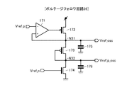
[ボルテージフォロワ回路28]
次に、ボルテージフォロワ回路28の具体的構成を図12を参照して説明する。
[Voltage follower circuit 28]
Next, a specific configuration of the
このボルテージフォロワ回路28は、差動増幅器171、pMOSトランジスタ172、173、nMOSトランジスタ174、及びキャパシタ175、176を備えて構成されている。
The
差動増幅器171は、一方の入力端子に、前述の出力電圧Vref_pを入力され、他方の入力端子はその出力端子(ノードN31)と接続されている。ノードN31は、出力電圧Vref_oscの出力端子である。また、トランジスタ172〜174は、電源端子と接地端子との間において、その順に直列接続されている。
In the
pMOSトランジスタ172のゲートは、前述の差動増幅器171の出力端子に接続されている。また、pMOSトランジスタ173のゲート(ノードN32)は、そのドレインと短絡されており、これが出力電圧Vref_p_oscの出力端子とされている。キャパシタ175、176は、ノードN31、N32と接地端子との間に接続されている。
The gate of the
これにより、このボルテージフォロワ回路28は、バンドギャップリファレンス回路27の出力電圧Vref_p、Vref_nを入力電圧として、出力電圧Vref_osc、Vref_p_oscを出力する機能を有する。
Thus, the
[動作]
次に、図13及び図14を参照して、このICドライバ20の動作を説明する。特に、出力電圧が変形電圧Vactから維持電圧Vholdに切り替わる段階における動作を詳しく説明する。
[Operation]
Next, the operation of the
MEMS型可変容量キャパシタ10の主電極14a、15a間の距離dを縮める場合には、制御信号ACT_Enが立ち上がり、これによりポンプ回路21Aが動作を開始し、出力ノードACTNODEの電圧が変形電圧Vactまで昇圧される(図13のステップS11)。ローカルポンプ回路25Aは、nMOSトランジスタ26Aを導通させるためのゲート電圧Vgaを出力し、これにより、変形電圧Vactは出力端子OUTに供給される。
When the distance d between the
なお、これと同時に、ポンプ回路21B、発振回路22B、リミッタ回路23B等も動作を開始し、出力ノードHOLDNODEの電圧を維持電圧Vholdまで充電する。ただし、ローカルポンプ回路25Bはゲート電圧Vgbを出力しておらず、従ってnMOSトランジスタ26Bは非導通状態とされている。
At the same time, the
その後、バンドギャップリファレンス回路27の抵抗144の抵抗値R2aが小さい値に変更されると、出力電圧Vbgr1がVvgr1´へと降圧を開始する(ステップS12、図14の時刻t11)。その後、ディスチャージ回路24Aが動作し、出力ノードACTNODEの電圧の電圧Vact2への低下が開始される(S13、時刻t12)。
Thereafter, when the resistance value R2a of the resistor 144 of the bandgap reference circuit 27 is changed to a small value, the output voltage Vbgr1 starts to step down to Vvgr1 ′ (step S12, time t11 in FIG. 14). Thereafter, the
こうして、出力ノードACTNODEの電圧が次の式で示される電圧Vact2まで低下し(ステップS14、時刻t13)、このディスチャージ回路24Aの動作開始から所定時間が経過した場合(ステップS15)、ディスチャージ回路24Aから制御信号DC_Ena=”L”が出力され、これにより、ローカルポンプ回路25Aの動作が停止(ディセーブル)されると共に、出力端子OUTLPaの電圧がディスチャージされる。
Thus, the voltage of the output node ACTNODE decreases to the voltage Vact2 expressed by the following equation (step S14, time t13), and when a predetermined time has elapsed from the start of the operation of the
これと同時に、ローカルポンプ回路25Bの動作が開始(イネーブル)される。これにより、nMOSトランジスタ26Aが非導通状態に切り替わる一方、nMOSトランジスタ26Bがこれに代わって導通状態に切り替わる。
At the same time, the operation of the
なお、出力ノードACTNODEの電圧がVactからVact2に低下するときの速度は、キャパシタC2の容量Cload、リミッタ回路23A内の抵抗53に流れるバイアス電流の値によって異なる。容量Cloadが大きく、リミッタ回路23Aのバイアス電流の値が小さい場合には、出力ノードACTNODEの電圧の変化する速度は遅くなる。一方、容量Cloadが小さく、リミッタ回路23Aのバイアス電流の値が大きい場合には、出力ノードACTNODEの電圧が変化する速度は速くなる。ステップS14とステップS15は、場合により前後が逆になる場合もある。
Note that the speed at which the voltage of the output node ACTNODE decreases from Vact to Vact2 varies depending on the capacitance Cload of the capacitor C2 and the value of the bias current flowing through the
このようにしてnMOSトランジスタ26Aが非導通状態に切り替わるが、このとき、nMOSトランジスタ26Aのソース−ドレイン間には、次の式であらわされる電圧Vswが印加される。
In this way, the
しかし、この実施の形態では、nMOSトランジスタ26Aの非導通状態への切り替わりの前に、出力ノードACTNODEのディスチャージ動作が開始されるので、この電圧Vswを小さくすることができる。これにより、nMOSトランジスタ26Aのチャネルホットエレクトロンによる特性劣化(閾値電圧の変化)により信頼性が損なわれる問題を回避できる。
However, in this embodiment, since the discharge operation of the output node ACTNODE is started before the
なお、電圧Vact2の値は、バンドギャップリファレンス回路27により任意に変更することができる。 The value of the voltage Vact2 can be arbitrarily changed by the band gap reference circuit 27.
[第2の実施の形態]
次に、本発明の第2の実施の形態に係る半導体集積回路を、図面を参照して説明する。この実施の形態の半導体集積回路の全体構成は、図1のと同様であり、また、ドライバIC20の構成も、図3に示すのと同様である。更に、ドライバIC20を構成する各回路の構成も、図4〜図12に示すのと同様である。
[Second Embodiment]
Next, a semiconductor integrated circuit according to a second embodiment of the present invention will be described with reference to the drawings. The overall configuration of the semiconductor integrated circuit of this embodiment is the same as that of FIG. 1, and the configuration of the
この実施の形態では、バンドギャップリファレンス回路27の構成が第1の実施の形態とは異なっている。ただし、異なる点は、電流I6とI7の大きさが次の数式で表現されるように設定されている点が第1の実施の形態とは異なるのみであるので、以下では、図11を参照しつつ説明を行う。 In this embodiment, the configuration of the band gap reference circuit 27 is different from that of the first embodiment. However, the only difference is that the currents I6 and I7 are set so that the magnitudes of the currents I6 and I7 can be expressed by the following mathematical formulas. However, an explanation will be given.
このような電流I6とI7の合計である電流Irefは、抵抗146を流れる。
この電流Irefは、発振回路22Aにおける発振周波数の安定化のため、電源電圧・温度・ばらつきに対して依存しにくい電流であることが要求される。
A current Iref that is the sum of the currents I6 and I7 flows through the
This current Iref is required to be a current that does not easily depend on the power supply voltage, temperature, and variations in order to stabilize the oscillation frequency in the
ここで、電流I1、I5は、次の式により表現される。 Here, the currents I1 and I5 are expressed by the following equations.
従って、電流Irefは、次の式で表現される。 Therefore, the current Iref is expressed by the following equation.
ここで、電流Irefの温度依存性を零にするためには、次の条件が満たされることが必要となる。 Here, in order to make the temperature dependence of the current Iref zero, it is necessary to satisfy the following condition.
このような条件を満たす、又は略満たすmの値となるよう、各回路要素のパラメータの設計を行う。ここで、抵抗が正の温度係数を持つとする。電流I5は、温度が上がるほど小さくなる。これは、抵抗154の抵抗値が上がるからである。これに対し、電流I1は、温度が上がるほど大きくなる。これは、抵抗132の抵抗値も大きくなるが、それ以上にダイオード133が電流を流しやすくするためである。従って、電流I1とI5について、各抵抗とダイオードの温度係数に合わせて設計した値mを用いて作成する電流Irefは温度依存に強い基準電流源となる。
The parameters of each circuit element are designed so that the value of m that satisfies or substantially satisfies such a condition. Here, it is assumed that the resistance has a positive temperature coefficient. The current I5 decreases as the temperature increases. This is because the resistance value of the
以上、発明の実施の形態を説明したが、本発明はこれらに限定されるものではなく、発明の趣旨を逸脱しない範囲内において、種々の変更、追加等が可能である。 Although the embodiments of the invention have been described above, the present invention is not limited to these embodiments, and various modifications and additions can be made without departing from the spirit of the invention.
10・・・MEMS型可変容量キャパシタ、 20・・・ドライバIC、 11・・・アンカー部、 12・・・可動部、 13・・・固定部、 14・・・上部電極、15・・・下部電極、 21A、21B・・・ポンプ回路、 22A、22B・・・発振回路、 23A、23B・・・リミッタ回路、 24A、24B・・・ディスチャージ回路、 25A、25B・・・ローカルポンプ回路、 26A、26B・・・nMOSトランジスタ。
DESCRIPTION OF
Claims (5)
電源電圧を第2電圧まで昇圧させる第2昇圧回路と、
前記第1電圧が出力される第1ノードに一端が接続され前記第1電圧を出力端子に転送する第1トランジスタと、
前記第2電圧が出力される第2ノードに一端が接続され前記第2電圧を前記出力端子に転送する第2トランジスタと、
前記第1電圧を更に昇圧させた第3電圧を前記第1トランジスタの制御端子に供給して前記第1トランジスタを導通させる第3昇圧回路と、
前記第2電圧を更に昇圧させた第4電圧を前記第2トランジスタの制御端子に供給して前記第2トランジスタを導通させる第4昇圧回路と、
前記第1ノードの電圧を所定の電圧まで放電させる第1ディスチャージ回路と、
前記出力端子の電圧を所定の電圧まで放電させる第2ディスチャージ回路と
を備え、
前記第3昇圧回路は、前記第1ノードの放電が開始された後の時点において、前記第1トランジスタの制御端子に供給する電圧を引き下げて前記第1トランジスタを非導通とし、
前記第4昇圧回路は、前記第1トランジスタが非導通とされた後、前記第3昇圧回路からの信号に従い前記第2トランジスタの制御端子に供給する電圧を引き上げて第2トランジスタを導通状態に切り換える
ことを特徴とする半導体集積回路。 A first booster circuit for boosting the power supply voltage to the first voltage;
A second booster circuit for boosting the power supply voltage to the second voltage;
A first transistor having one end connected to a first node from which the first voltage is output and transferring the first voltage to an output terminal;
A second transistor having one end connected to a second node from which the second voltage is output and transferring the second voltage to the output terminal;
A third booster circuit that further boosts the first voltage to supply a control terminal of the first transistor to make the first transistor conductive;
A fourth booster circuit that further boosts the second voltage to supply a control terminal of the second transistor to make the second transistor conductive;
A first discharge circuit for discharging the voltage of the first node to a predetermined voltage;
A second discharge circuit for discharging the voltage of the output terminal to a predetermined voltage,
The third booster circuit lowers the voltage supplied to the control terminal of the first transistor at a time after the discharge of the first node is started to make the first transistor non-conductive,
The fourth booster circuit switches the second transistor to a conductive state by raising the voltage supplied to the control terminal of the second transistor in accordance with a signal from the third booster circuit after the first transistor is turned off. A semiconductor integrated circuit.
前記基準電位を発生させるための基準電位発生回路を備え、
前記基準電位発生回路は、
電源電圧に依存しない電流を発生させる電流発生回路と、
前記電流を流す可変抵抗と
を備え、
前記可変抵抗の抵抗値を変化させることにより前記基準電圧の値を変更可能に構成された
ことを特徴とする請求項1記載の半導体集積回路。 A limiter circuit that outputs a limiter signal for stopping the operation of the first booster circuit based on a result of comparison between a voltage corresponding to the voltage of the first node and a reference potential;
A reference potential generating circuit for generating the reference potential;
The reference potential generation circuit includes:
A current generation circuit for generating a current independent of the power supply voltage;
A variable resistor for passing the current, and
2. The semiconductor integrated circuit according to claim 1, wherein the value of the reference voltage can be changed by changing a resistance value of the variable resistor.
電源電圧を第2電圧まで昇圧させる第2昇圧回路と、
前記第1電圧が出力される第1ノードに一端が接続され前記第1電圧を出力端子に転送する第1トランジスタと、
前記第2電圧が出力される第2ノードに一端が接続され前記第2電圧を前記出力端子に転送する第2トランジスタと、
前記第1電圧を更に昇圧させた第3電圧を前記第1トランジスタの制御端子に供給して前記第1トランジスタを導通させる第3昇圧回路と、
前記第2電圧を更に昇圧させた第4電圧を前記第2トランジスタの制御端子に供給して前記第2トランジスタを導通させる第4昇圧回路と、
前記第1ノードの電圧を所定の電圧まで放電させる第1ディスチャージ回路と、
前記出力端子の電圧を所定の電圧まで放電させる第2ディスチャージ回路と
前記第1ノードの電圧に対応する電圧と基準電位との比較の結果に基づいて、前記第1 昇圧回路の動作を停止させるリミッタ信号を出力するリミッタ回路と、
前記基準電位を発生させるための基準電位発生回路と
を備え、
前記基準電位発生回路は、
第3ノードと接地電位との間に第1のpMOSトランジスタ、第1の抵抗及び第1のダイオードをその順に直列接続してなる第1電流経路と、
前記第3ノードと接地電位との間に第2のpMOSトランジスタ、第2の抵抗、第3の抵抗及びN個の並列接続ダイオードをその順に直列接続してなる第2電流経路と、
前記第3ノードと接地電位との間に第3のpMOSトランジスタ及び第1の可変抵抗を直列接続してなる第3の電流経路と、
第3ノードと電源電圧と間に接続された第4のpMOSトランジスタと、
前記第1、第2、及び第3のpMOSトランジスタのゲートを第1入力端子に接続される一方前記第1のpMOSトランジスタと前記第1の抵抗との接続点を第2入力端子に接続されてその差動信号を前記第4のpMOSトランジスタのゲートに出力する第1の差動増幅器と
を備え、
前記第1の可変抵抗は、前記第1ノードの電圧が前記第1の電圧に達した後の時点において第1の値からこの第1の値よりも低い第2の値に切り換えられるように構成された
ことを特徴とする半導体集積回路。 A first booster circuit for boosting the power supply voltage to the first voltage;
A second booster circuit for boosting the power supply voltage to the second voltage;
A first transistor having one end connected to a first node from which the first voltage is output and transferring the first voltage to an output terminal;
A second transistor having one end connected to a second node from which the second voltage is output and transferring the second voltage to the output terminal;
A third booster circuit that further boosts the first voltage to supply a control terminal of the first transistor to make the first transistor conductive;
A fourth booster circuit that further boosts the second voltage to supply a control terminal of the second transistor to make the second transistor conductive;
A first discharge circuit for discharging the voltage of the first node to a predetermined voltage;
A second discharge circuit that discharges the voltage of the output terminal to a predetermined voltage, and a limiter that stops the operation of the first booster circuit based on a result of comparison between a voltage corresponding to the voltage of the first node and a reference potential A limiter circuit for outputting a signal;
A reference potential generation circuit for generating the reference potential,
The reference potential generation circuit includes:
A first current path formed by connecting a first pMOS transistor, a first resistor, and a first diode in series between the third node and the ground potential in that order;
A second current path formed by serially connecting a second pMOS transistor, a second resistor, a third resistor, and N parallel-connected diodes in that order between the third node and the ground potential;
A third current path formed by connecting a third pMOS transistor and a first variable resistor in series between the third node and the ground potential;
A fourth pMOS transistor connected between the third node and the power supply voltage;
The gates of the first, second and third pMOS transistors are connected to a first input terminal, while the connection point of the first pMOS transistor and the first resistor is connected to a second input terminal. A first differential amplifier that outputs the differential signal to the gate of the fourth pMOS transistor;
The first variable resistor is configured to be switched from a first value to a second value lower than the first value at a time after the voltage of the first node reaches the first voltage. A semiconductor integrated circuit characterized by that.
電源電圧を第2電圧まで昇圧させる第2昇圧回路と、
前記第1電圧が出力される第1ノードに一端が接続され前記第1電圧を出力端子に転送する第1トランジスタと、
前記第2電圧が出力される第2ノードに一端が接続され前記第2電圧を前記出力端子に転送する第2トランジスタと、
前記第1電圧を更に昇圧させた第3電圧を前記第1トランジスタの制御端子に供給して前記第1トランジスタを導通させる第3昇圧回路と、
前記第2電圧を更に昇圧させた第4電圧を前記第2トランジスタの制御端子に供給して前記第2トランジスタを導通させる第4昇圧回路と、
前記第1ノードの電圧を所定の電圧まで放電させる第1ディスチャージ回路と、
前記出力端子の電圧を所定の電圧まで放電させる第2ディスチャージ回路と
前記第1ノードの電圧に対応する電圧と基準電位との比較の結果に基づいて、前記第1ディスチャージ回路を動作させるためのリミッタ信号を出力するリミッタ回路と、
前記基準電位を発生させるための基準電位発生回路を備え、
前記基準電位発生回路は、
第3ノードと接地電位との間に第1のpMOSトランジスタ、第1の抵抗及び第1のダイオードをその順に直列接続してなる第1電流経路と、
前記第3ノードと接地電位との間に第2のpMOSトランジスタ、第2の抵抗、第3の抵抗及びN個の並列接続ダイオードをその順に直列接続してなる第2電流経路と、
前記第3ノードと接地電位との間に第3のpMOSトランジスタ及び第1の可変抵抗を直列接続すると共に第4ノードと前記第3のpMOSトランジスタのドレインとの間に第4のpMOSトランジスタを接続してなる第3の電流経路と、
前記第3ノードと接地電位との間に第5のpMOSトランジスタ及び第2の可変抵抗を直列接続すると共に前記第4ノードと前記第5のPMOSトランジスタのドレインとの間に第6のpMOSトランジスタを接続してなる第4の電流経路と、
前記第3ノードと第5ノードとの間に第7のpMOSトランジスタを接続する一方前記第4ノードと前記第5ノードとの間に第8のpMOSトランジスタを接続し、且つ前記第5ノードと接地電位との間に第4の抵抗とダイオード接続された第1のnMOSトランジスタをその順に接続してなる第5の電流経路と、
前記第4ノードと接地電位との間に第9のpMOSトランジスタ及び第5の抵抗をその順に直列接続してなる第6の電流経路と、
第3ノードと電源電圧と間に接続された第10のpMOSトランジスタと、
前記第1、第2、第3、第5及び第7のpMOSトランジスタのゲートを第1入力端子に接続される一方前記第1のpMOSトランジスタと前記第1の抵抗との接続点である第6ノードを第2入力端子に接続されてその差動信号を前記第10のpMOSトランジスタのゲートに出力する第1の差動増幅器と、
前記第6ノードを第1入力端子に接続される一方前記第9のpMOSトランジスタ及び前記第5の抵抗の接続点である第7ノードを第2入力端子に接続されその差動信号を前記第4、第5、第8、及び第9のpMOSトランジスタのゲートに出力する第2の差動増幅器と
を備え、
前記第1の可変抵抗は、前記第1ノードの電圧が前記第1の電圧に達した後の時点において第1の値からこの第1の値よりも低い第2の値に切り換えられるように構成された
ことを特徴とする半導体集積回路。 A first booster circuit for boosting the power supply voltage to the first voltage;
A second booster circuit for boosting the power supply voltage to the second voltage;
A first transistor having one end connected to a first node from which the first voltage is output and transferring the first voltage to an output terminal;
A second transistor having one end connected to a second node from which the second voltage is output and transferring the second voltage to the output terminal;
A third booster circuit that further boosts the first voltage to supply a control terminal of the first transistor to make the first transistor conductive;
A fourth booster circuit that further boosts the second voltage to supply a control terminal of the second transistor to make the second transistor conductive;
A first discharge circuit for discharging the voltage of the first node to a predetermined voltage;
A second discharge circuit for discharging the voltage at the output terminal to a predetermined voltage; and a limiter for operating the first discharge circuit based on a result of comparison between a voltage corresponding to the voltage at the first node and a reference potential. A limiter circuit for outputting a signal;
A reference potential generating circuit for generating the reference potential;
The reference potential generation circuit includes:
A first current path formed by connecting a first pMOS transistor, a first resistor, and a first diode in series between the third node and the ground potential in that order;
A second current path formed by serially connecting a second pMOS transistor, a second resistor, a third resistor, and N parallel-connected diodes in that order between the third node and the ground potential;
A third pMOS transistor and a first variable resistor are connected in series between the third node and the ground potential, and a fourth pMOS transistor is connected between the fourth node and the drain of the third pMOS transistor. And a third current path,
A fifth pMOS transistor and a second variable resistor are connected in series between the third node and the ground potential, and a sixth pMOS transistor is connected between the fourth node and the drain of the fifth PMOS transistor. A connected fourth current path;
A seventh pMOS transistor is connected between the third node and the fifth node, while an eighth pMOS transistor is connected between the fourth node and the fifth node, and the fifth node and the ground. A fifth current path formed by connecting, in that order, a first nMOS transistor that is diode-connected to a fourth resistor between the potential and
A sixth current path in which a ninth pMOS transistor and a fifth resistor are connected in series in that order between the fourth node and the ground potential;
A tenth pMOS transistor connected between the third node and the power supply voltage;
The gates of the first, second, third, fifth and seventh pMOS transistors are connected to the first input terminal, while the sixth pMOS transistor is a connection point between the first pMOS transistor and the first resistor. A first differential amplifier having a node connected to a second input terminal and outputting the differential signal to the gate of the tenth pMOS transistor;
The sixth node is connected to the first input terminal, while the seventh node, which is the connection point of the ninth pMOS transistor and the fifth resistor, is connected to the second input terminal, and the differential signal is sent to the fourth input terminal. A second differential amplifier that outputs to the gates of the fifth, eighth, and ninth pMOS transistors,
The first variable resistor is configured to be switched from a first value to a second value lower than the first value at a time after the voltage of the first node reaches the first voltage. A semiconductor integrated circuit characterized by that.
Priority Applications (2)
| Application Number | Priority Date | Filing Date | Title |
|---|---|---|---|
| JP2008297619A JP5361346B2 (en) | 2008-11-21 | 2008-11-21 | Semiconductor integrated circuit |
| US12/556,937 US7834681B2 (en) | 2008-11-21 | 2009-09-10 | Semiconductor integrated circuit |
Applications Claiming Priority (1)
| Application Number | Priority Date | Filing Date | Title |
|---|---|---|---|
| JP2008297619A JP5361346B2 (en) | 2008-11-21 | 2008-11-21 | Semiconductor integrated circuit |
Publications (2)
| Publication Number | Publication Date |
|---|---|
| JP2010123837A JP2010123837A (en) | 2010-06-03 |
| JP5361346B2 true JP5361346B2 (en) | 2013-12-04 |
Family
ID=42195665
Family Applications (1)
| Application Number | Title | Priority Date | Filing Date |
|---|---|---|---|
| JP2008297619A Expired - Fee Related JP5361346B2 (en) | 2008-11-21 | 2008-11-21 | Semiconductor integrated circuit |
Country Status (2)
| Country | Link |
|---|---|
| US (1) | US7834681B2 (en) |
| JP (1) | JP5361346B2 (en) |
Families Citing this family (7)
| Publication number | Priority date | Publication date | Assignee | Title |
|---|---|---|---|---|
| US9237296B2 (en) * | 2009-06-01 | 2016-01-12 | Lg Electronics Inc. | Image display apparatus and operating method thereof |
| JP5537180B2 (en) * | 2010-02-16 | 2014-07-02 | 株式会社東芝 | Electrostatic actuator device |
| JP5591629B2 (en) * | 2010-08-30 | 2014-09-17 | 株式会社東芝 | Semiconductor device and driving method of electrostatic actuator |
| JP2012186784A (en) * | 2010-12-24 | 2012-09-27 | Renesas Electronics Corp | Crystal oscillation device and semiconductor device |
| WO2014186656A1 (en) * | 2013-05-17 | 2014-11-20 | Cavendish Kinetics, Inc | Method and technique to control mems dvc control waveform for lifetime enhancement |
| FR3045982B1 (en) * | 2015-12-18 | 2019-06-14 | Commissariat A L'energie Atomique Et Aux Energies Alternatives | LOGIC CELL WITH LOW CONSUMPTION |
| KR20220148518A (en) * | 2021-04-29 | 2022-11-07 | 에스케이하이닉스 주식회사 | Monitoring circuit monitoring performance of transistors |
Family Cites Families (12)
| Publication number | Priority date | Publication date | Assignee | Title |
|---|---|---|---|---|
| DE69327164T2 (en) * | 1993-09-30 | 2000-05-31 | St Microelectronics Srl | Booster circuit for generating positive and negative increased voltages |
| JP3167904B2 (en) * | 1994-12-27 | 2001-05-21 | 日本鋼管株式会社 | Voltage booster circuit |
| JP3586073B2 (en) * | 1997-07-29 | 2004-11-10 | 株式会社東芝 | Reference voltage generation circuit |
| JP3910765B2 (en) * | 1999-09-08 | 2007-04-25 | 株式会社東芝 | Voltage generation circuit and voltage transfer circuit using the same |
| US6255896B1 (en) * | 1999-09-27 | 2001-07-03 | Intel Corporation | Method and apparatus for rapid initialization of charge pump circuits |
| JP3872927B2 (en) * | 2000-03-22 | 2007-01-24 | 株式会社東芝 | Booster circuit |
| FI109155B (en) * | 2000-04-13 | 2002-05-31 | Nokia Corp | Method and arrangement for controlling a micromechanical element |
| JP2002074956A (en) * | 2000-09-04 | 2002-03-15 | Mitsubishi Electric Corp | Semiconductor device |
| JP4109831B2 (en) * | 2001-01-15 | 2008-07-02 | 株式会社東芝 | Semiconductor device |
| US7595682B2 (en) * | 2005-02-24 | 2009-09-29 | Macronix International Co., Ltd. | Multi-stage charge pump without threshold drop with frequency modulation between embedded mode operations |
| US7248521B2 (en) * | 2005-07-12 | 2007-07-24 | Micron Technology, Inc. | Negative voltage discharge scheme to improve snapback in a non-volatile memory |
| JP4808069B2 (en) * | 2006-05-01 | 2011-11-02 | 富士通セミコンダクター株式会社 | Reference voltage generator |
-
2008
- 2008-11-21 JP JP2008297619A patent/JP5361346B2/en not_active Expired - Fee Related
-
2009
- 2009-09-10 US US12/556,937 patent/US7834681B2/en not_active Expired - Fee Related
Also Published As
| Publication number | Publication date |
|---|---|
| US20100127764A1 (en) | 2010-05-27 |
| US7834681B2 (en) | 2010-11-16 |
| JP2010123837A (en) | 2010-06-03 |
Similar Documents
| Publication | Publication Date | Title |
|---|---|---|
| JP5361346B2 (en) | Semiconductor integrated circuit | |
| US7304530B2 (en) | Utilization of device types having different threshold voltages | |
| US7199641B2 (en) | Selectably boosted control signal based on supply voltage | |
| JP4288434B2 (en) | High voltage generation circuit | |
| KR101194940B1 (en) | Ldo regulators for integrated applications | |
| US7893778B2 (en) | Flexible low current oscillator for multiphase operations | |
| JP4424546B2 (en) | Pulse width modulation circuit | |
| US20090195227A1 (en) | Constant voltage circuit | |
| US8981750B1 (en) | Active regulator wake-up time improvement by capacitive regulation | |
| JP6376961B2 (en) | DC / DC converter | |
| JP2014206825A (en) | Bias circuit | |
| KR20100020208A (en) | Negative supply voltage generating circuit and semiconductor integrated circuit having the same | |
| US10476383B2 (en) | Negative charge pump circuit | |
| TWI672572B (en) | Voltage Regulator | |
| JP4824599B2 (en) | Triangular wave generation circuit | |
| US20150214837A1 (en) | Charge pump circuit | |
| US11139004B2 (en) | Charge pump circuit and auxiliary power supply | |
| JP2012227588A (en) | Comparison circuit and analog-digital conversion circuit | |
| EP2587649A1 (en) | Control signal generating circuit, charge pump drive circuit, clock driver, and method of driving charge pump | |
| WO2022045106A1 (en) | Comparator, oscillator, and power converter | |
| TWI436593B (en) | High-precision oscillator systems with feed forward compensation for ccfl driver systems and methods thereof | |
| JPH09294367A (en) | Voltage supply circuit | |
| TW201534029A (en) | Initialization device, integrated circuit, and method of operating a charge pump | |
| CN113169667B (en) | Charge pump circuit and voltage conversion method | |
| CN111181385B (en) | Negative voltage circuit |
Legal Events
| Date | Code | Title | Description |
|---|---|---|---|
| A621 | Written request for application examination |
Free format text: JAPANESE INTERMEDIATE CODE: A621 Effective date: 20110314 |
|
| RD01 | Notification of change of attorney |
Free format text: JAPANESE INTERMEDIATE CODE: A7421 Effective date: 20130221 |
|
| A977 | Report on retrieval |
Free format text: JAPANESE INTERMEDIATE CODE: A971007 Effective date: 20130424 |
|
| A131 | Notification of reasons for refusal |
Free format text: JAPANESE INTERMEDIATE CODE: A131 Effective date: 20130430 |
|
| A521 | Written amendment |
Free format text: JAPANESE INTERMEDIATE CODE: A523 Effective date: 20130627 |
|
| TRDD | Decision of grant or rejection written | ||
| A01 | Written decision to grant a patent or to grant a registration (utility model) |
Free format text: JAPANESE INTERMEDIATE CODE: A01 Effective date: 20130806 |
|
| A61 | First payment of annual fees (during grant procedure) |
Free format text: JAPANESE INTERMEDIATE CODE: A61 Effective date: 20130903 |
|
| LAPS | Cancellation because of no payment of annual fees |