JP5345956B2 - System and apparatus for diagnostic monitoring of optical modulation amplitude using automatic gain control in an optical receiver - Google Patents
System and apparatus for diagnostic monitoring of optical modulation amplitude using automatic gain control in an optical receiver Download PDFInfo
- Publication number
- JP5345956B2 JP5345956B2 JP2010008865A JP2010008865A JP5345956B2 JP 5345956 B2 JP5345956 B2 JP 5345956B2 JP 2010008865 A JP2010008865 A JP 2010008865A JP 2010008865 A JP2010008865 A JP 2010008865A JP 5345956 B2 JP5345956 B2 JP 5345956B2
- Authority
- JP
- Japan
- Prior art keywords
- optical
- signal
- output
- signal level
- circuit
- Prior art date
- Legal status (The legal status is an assumption and is not a legal conclusion. Google has not performed a legal analysis and makes no representation as to the accuracy of the status listed.)
- Active
Links
Images


Classifications
-
- H—ELECTRICITY
- H04—ELECTRIC COMMUNICATION TECHNIQUE
- H04B—TRANSMISSION
- H04B10/00—Transmission systems employing electromagnetic waves other than radio-waves, e.g. infrared, visible or ultraviolet light, or employing corpuscular radiation, e.g. quantum communication
- H04B10/07—Arrangements for monitoring or testing transmission systems; Arrangements for fault measurement of transmission systems
- H04B10/075—Arrangements for monitoring or testing transmission systems; Arrangements for fault measurement of transmission systems using an in-service signal
- H04B10/077—Arrangements for monitoring or testing transmission systems; Arrangements for fault measurement of transmission systems using an in-service signal using a supervisory or additional signal
- H04B10/0779—Monitoring line transmitter or line receiver equipment
Description
従来の光通信システムが図1に例示されている。この光通信システム1は、送信機10、光媒体20(例えば、光ファイバー、導波路、自由空間、など)、及び受信機30から構成されている。光通信システム1は、接続部5の入力データを受け取り、接続部35に与えられた出力データを発生する。送信機10は、データ入力12と光出力14を備えている。受信機30は、光入力32とデータ出力34を備えている。光媒体20は、光出力14に接続されている第1の端部22と、光入力32に接続されている第2の端部24を有している。送信機10は電気的フォーマットでデータを受け取り、光媒体20上で振幅変調された光表示(optical representation)データと結合している。受信機30は、振幅変調された光表示データを光媒体20から受け取り、そのデータを受信されたデータの電気的表現あるいは表示(representation)に変換する。
A conventional optical communication system is illustrated in FIG. The
データ信号の光変調振幅(OMA: optical modulation amplitude)は、ディジタル通信システムで使用される光リンクの性能を規定する場合に用いられる重要なパラメータである。所定の受信機の雑音レベル(noise floor)では、OMAは通信システムのビットエラー率(BER)に直接関係する。 An optical modulation amplitude (OMA) of a data signal is an important parameter used when defining the performance of an optical link used in a digital communication system. For a given receiver noise floor, OMA is directly related to the bit error rate (BER) of the communication system.
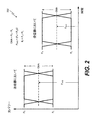
バイポーラの非ゼロ復帰(NRZ)光信号方式では、わずか2つの別個の光パワーレベル、ハイレベルすなわちPH及びローレベルすなわちPL、しか使用されない。図2は、図1の送信機10と受信機30の両方に対する光パワー対時間のプロット200を示している。図2に例示されているように、OMAはハイとローのパワーレベル間の差として定義され、これは数学的に下記のように表すことができる。
OMA=PH−PL 式1
平均信号パワーは、ハイ及びローのパワーレベルを単純に平均したものである。すなわち、
PAVG=(PH+PL)/2 式2
消光比(ER: extinction ratio)は、ハイ及びローのパワーレベル間の比である。
ER=PH/PL 式3
式1、式2、及び式3から、次の関係式を引き出すことができる。
OMA=2PAVG[(ER−1)/(ER+1)] 式4
In a non-return-to-zero (NRZ) optical signaling bipolar, only two discrete light power level, a high level i.e. P H and a low level i.e. P L, only be used. FIG. 2 shows a
OMA = P H -P L Formula 1
The average signal power is simply the average of the high and low power levels. That is,
P AVG = (P H + P L ) / 2
The extinction ratio (ER) is the ratio between high and low power levels.
ER = P H / P L Formula 3
From
OMA = 2P AVG [(ER-1) / (ER + 1)] Equation 4
OMAとERは、それらがそれぞれパワーレベルの差と比率を規定するため、それら自身は相対的な数値である。OMA又はERから絶対数値を得るためには、PAVG、PH、又はPLなどの付加的な基準点が必要である。式3及び式4によって定義されたそれぞれの関係式は、これらの付加的な基準点の1つに依存する。 OMA and ER are themselves relative numbers because they define the power level difference and ratio, respectively. In order to obtain absolute values from OMA or ER, additional reference points such as P AVG , P H , or P L are required. Each relation defined by Equation 3 and Equation 4 depends on one of these additional reference points.
例えば、100μWのOMAは、PAVG、PH、又はPLに対して無数の可能な値に対応することができる。PHは、PLが0μWに等しい場合は100μW、又はPLが50μWの場合は、PHは150μW、又はPLが99.9mWの場合は、PHは100mWとすることができる。 For example, 100 μW OMA can correspond to innumerable possible values for P AVG , P H , or P L. P H is, 100 .mu.W if P L is equal to 0MyuW, or if P L is 50 W, P H is 150MyuW, or P L is 99.9mW is, P H may be 100 mW.
ERの代わりの場合には、ER=10を用いる同様の実施例が、PAVG、PH、又はPLに対して無数の可能な値に対応することができる。PLが10μWの場合、PHは100μW、又はPLが15μWの場合、PHは150μW、又はPLが10mWの場合、PHは100mWにすることができる。 In the alternative case of ER, a similar embodiment using ER = 10 may correspond to the myriad possible values for P AVG , P H , or P L. If P L is 10 .mu.W, P H is 100 .mu.W, or P L is 15MyuW, if P H is 150MyuW, or P L is 10 mW, P H can be 100 mW.
OMA及びERに加えてPAVG=100μWの基準点が指定される場合、あいまいさが取り除かれる。OMAが100μWでかつPAVG=100μWの場合、PHは150μW、PLは50μWの値しか取ることができない。ERが10で、かつPAVG=100μWの場合、PHは182μW、PLは18.2μWの値しか取ることができない。 If a reference point of P AVG = 100 μW is specified in addition to OMA and ER, the ambiguity is removed. If OMA is a and P AVG = 100μW 100μW, P H is 150μW, P L can not take only the value of 50 W. ER is at 10, and if the P AVG = 100μW, P H is 182μW, P L can not take only the value of 18.2MyuW.
OMAとERはほぼ等価であることが明白のように思えるが、相違が存在する。これらの相違の1つは、信号が光通信システムを通って伝搬するときに、OMAとERが変化する方法である。光通信システムが2点間で線形の減衰を示すと仮定すると、ERは信号が減衰されるため一定にとどまるが、OMAは減衰に等しいファクタで変化する。例えば、減衰が0.3dB/kmで10km以上の光ファイバーの場合、10kmの全減衰量は3dBであり、これは1/2に相当する。PHが1mW及びPLが0.1mWで開始する光ファイバーを通って送信される信号は、光ファイバーの入力では、ERは1/0.1=10であり、OMA=1−0.1=0.90mWである。光ファイバーの出力では、PHは0.5mWであり、PLは0.05mWである(両方とも1/2に減少される)。このため、ERは0.5/0.05=10であり、OMA=0.5−0.05=0.45mWである。従って、ERは同じ値であるが、OMAは1/2に低減される。一旦ERが分かると、光通信システム内のどこからでも、平均電力を測定することにより、PH、PL及びOMAを計算するための十分な情報がもたらされる。他方においては、システム内の任意の点におけるOMAを測定しても、減衰の大きさを知ること又は付加的なパラメータ(PAVG、PH、又はPLなど)を測定することを行わない場合は、システム内の別の点におけるOMAを決定するための十分な情報は提供されない。 Although it seems obvious that OMA and ER are almost equivalent, there are differences. One of these differences is how the OMA and ER change as the signal propagates through the optical communication system. Assuming that the optical communication system exhibits linear attenuation between two points, ER remains constant as the signal is attenuated, but OMA varies with a factor equal to attenuation. For example, in the case of an optical fiber with attenuation of 0.3 dB / km and 10 km or more, the total attenuation of 10 km is 3 dB, which corresponds to 1/2. Signal P H is 1mW and P L are transmitted through the optical fiber starts at 0.1mW, in the input optical fiber, ER is 1 / 0.1 = 10, OMA = 1-0.1 = 0 .90mW. The output of the optical fiber, P H is 0.5 mW, P L is (are reduced to 1/2 both) a is 0.05 mW. For this reason, ER is 0.5 / 0.05 = 10 and OMA = 0.5-0.05 = 0.45 mW. Therefore, ER is the same value, but OMA is reduced to 1/2. Once the ER is known, measuring the average power from anywhere in the optical communication system provides enough information to calculate P H , P L and OMA. On the other hand, measuring OMA at any point in the system does not know the magnitude of the attenuation or measure additional parameters (such as P AVG , P H , or P L ) Does not provide enough information to determine the OMA at another point in the system.
光通信リンクのBER性能を最適化するためには、OMAはできるだけ大きくなければならない。光通信リンクでは、PAVGとOMAに上限と下限がある。光受信機では、受け取ることができる光パワーには上限がある。受信された光パワーがこの上限を超えると、飽和効果がBER性能を劣化することになる。最適な受信機のBER性能に関して、OMAはパワーの上限を避けながら、できるだけ大きいことが必要であり、これはPLがゼロで、かつPHがパワーの上限の直ぐ下にある場合に発生する。光源にレーザを使用する光送信機に関しては、PLをゼロに低減することは困難である。レーザが完全にオフ状態からオン状態に切り換えられる場合、ターンオン遅延と弛張発振が通信リンクに悪影響を与える。レーザがそのしきい値レベル以上にバイアスされて、それが常にオンである場合、ターンオン遅延と弛張発振の問題は減少される。このため、実際的なレーザ送信機は、PLで幾分かの光パワーを放射する。複雑にする要素は、レーザのしきい値が温度で大きく変化するため、バイアスとしきい値との間の差を一定に維持することが困難になることである。広い温度範囲にわたってバイアス電流を正確に制御することは、光送信機に対して相当な複雑性と費用を加えることになる。 In order to optimize the BER performance of the optical communication link, the OMA must be as large as possible. In an optical communication link, there are upper and lower limits for PAVG and OMA. In an optical receiver, there is an upper limit to the optical power that can be received. If the received optical power exceeds this upper limit, the saturation effect will degrade the BER performance. With respect to optimal receiver BER performance, OMA while avoiding the upper limit of power, it is necessary that as large as possible, which occurs when the P L is zero, and P H is just below the upper limit of power . For the optical transmitter using a laser as a light source, it is difficult to reduce the P L to zero. When the laser is completely switched from the off state to the on state, the turn-on delay and relaxation oscillation adversely affect the communication link. If the laser is biased above its threshold level and it is always on, turn-on delay and relaxation oscillation problems are reduced. Thus, a practical laser transmitter emits some optical power at P L. The complicating factor is that the laser threshold varies greatly with temperature, making it difficult to keep the difference between the bias and threshold constant. Accurate control of the bias current over a wide temperature range adds considerable complexity and cost to the optical transmitter.
比較的低損失のマルチモード・ファイバーを通信媒体として使用する従来の光通信リンクに対して、送信機におけるERと平均パワーの組合せにより、通信リンクの品質に適切な基準が提供されてきた。コアが大きいファイバー(例えば、ポリマー光ファイバー(POF))を使用する光通信用アプリケーションに対して、送信機におけるERと平均パワーの組合せは、光通信リンクの品質に対して十分な手段を提供していない。POFは安価であり、一般的なツールや普通の研磨紙を用いて容易に終端させることができるが、シリカで作られた同じ長さの光ファイバーと比較すると、POFは減衰量が大きくかつ帯域幅が狭い。POFを用いる通信リンクは、信号速度が高速電気通信用アプリケーションで使用されるものよりも遙かに遅い産業用制御アブレーション、ロボット、及び自動車用アプリケーションで使用されている。単純で安価な発光ダイオード(LED)ベースの送信機を可能にする比較的遅い信号速度は、POF通信ベースのシステムを市場が受け入れる及び市場に浸透する場合の重要な要因となることが証明されている。しかしながら、産業用オートメーションの用途では、最大長さ50メートルのPOFリンク及び最大長さ100メートルのハード・クラッデド・シリカ(HCS: hard cladded silica)リンクに対して、ファースト・イーサネット(登録商標)・データ送信プロトコル(Fast Ethernet data transfer protocol)(100Mbps)を使用するという要求がある。これらの距離を超える場合、標準的な開口数(NA: numerical aperture)が0.5のPOF及びNAが0.37のHCSリンクの帯域幅は、ファースト・イーサネット(登録商標)通信に対応していない。POF及びHCSを用いる通信リンクの帯域幅が限定されているため、望ましい最大の距離においてさえ、送信機におけるERと平均パワーの組合せが、通信リンクの品質の指標(measure)として役に立たないものにされてしまう。これは、受信された平均光パワーは公称値とすることができるが、通信媒体におけるモード分散(modal dispersion)が、受信機におけるハイとローの信号レベル間の差を減少させることがあるためである。ハイとローの信号レベル間の差がそのように減少することにより、通信リンクのBER性能がひどく劣化される可能性がある。 For conventional optical communication links that use relatively low loss multimode fiber as the communication medium, the combination of ER and average power at the transmitter has provided an appropriate reference to the quality of the communication link. For optical communications applications that use large core fibers (eg, polymer optical fiber (POF)), the combination of ER and average power at the transmitter provides a sufficient means for the quality of the optical communications link. Absent. Although POF is inexpensive and can be easily terminated using common tools and ordinary abrasive paper, POF has a higher attenuation and bandwidth compared to an optical fiber of the same length made of silica. Is narrow. Communication links using POF are used in industrial control ablation, robotic, and automotive applications where the signal speed is much slower than that used in high speed telecommunications applications. The relatively slow signal speed that enables simple and inexpensive light emitting diode (LED) based transmitters has proven to be an important factor in the market acceptance and penetration of POF communication based systems. Yes. However, in industrial automation applications, Fast Ethernet data for POF links up to 50 meters in length and hard claded silica (HCS) links up to 100 meters in length. There is a requirement to use a Fast Ethernet data transfer protocol (100 Mbps). When these distances are exceeded, the bandwidth of POF with a standard numerical aperture (NA) of 0.5 and HCS link with NA of 0.37 is compatible with Fast Ethernet communication. Absent. Due to the limited bandwidth of communication links using POF and HCS, the combination of ER and average power at the transmitter is useless as a measure of communication link quality, even at the desired maximum distance. End up. This is because the average optical power received can be nominal, but modal dispersion in the communication medium can reduce the difference between high and low signal levels at the receiver. is there. Such a reduction in the difference between the high and low signal levels can severely degrade the BER performance of the communication link.
光受信機システムの実施形態が、受信機の信号出力以外の場所でOMAの診断用評価値(diagnostic measure)を提供する。この光受信機システムは、入力の光信号に対応する電流を発生する光検出器に接続された入力を備えている。光受信機システムは、トランスインピーダンス増幅器及び回路をさらに備えている。このトランスインピーダンス増幅器は電流を受け取り、増幅された電圧を発生する。トランスインピーダンス増幅器は、自動利得制御を用いてトランスインピーダンス増幅器の出力が確実に制限されないようにする。すなわち、この自動利得制御は、トランスインピーダンス増幅器が確実に飽和されないようにする。回路は、トランスインピーダンス増幅器によって与えられた増幅された電圧と利得に関する指示を受け取る。この回路は、トランスインピーダンス増幅器によって与えられた電流と利得の関数として、第1の信号レベルと第2の信号レベルとの差を発生する。この回路は、OMAの診断用評価値を提供する。 Embodiments of the optical receiver system provide an OMA diagnostic measure at locations other than the signal output of the receiver. The optical receiver system includes an input connected to a photodetector that generates a current corresponding to the input optical signal. The optical receiver system further comprises a transimpedance amplifier and a circuit. The transimpedance amplifier receives the current and generates an amplified voltage. The transimpedance amplifier uses automatic gain control to ensure that the output of the transimpedance amplifier is not limited. That is, this automatic gain control ensures that the transimpedance amplifier is not saturated. The circuit receives an indication regarding the amplified voltage and gain provided by the transimpedance amplifier. This circuit produces a difference between the first signal level and the second signal level as a function of the current and gain provided by the transimpedance amplifier. This circuit provides a diagnostic evaluation value for OMA.
光受信機システムの別の実施形態は、受信機の信号出力以外の場所でOMAに関する診断用評価値を提供する。この光受信機システムは、入力の光信号に対応する電流を発生する光検出器に接続された入力を備えている。この光受信機システムは、信号ミラー(signal mirror)、トランスインピーダンス増幅器及び回路をさらに備えている。信号ミラーは電流に接続され、電流の第1及び第2の表示あるいは表現(representation)を信号ミラーのそれぞれの出力に転送する。トランスインピーダンス増幅器は電流を受信して、増幅された電圧を発生する。回路は、回路の入力で電流の表示を受け取り、第1の信号レベルの平均と第2の信号レベルの第2の平均との間の差を発生する。この差が、回路の出力においてOMAの診断用評価値を提供する。 Another embodiment of the optical receiver system provides diagnostic evaluation values for OMA at locations other than the signal output of the receiver. The optical receiver system includes an input connected to a photodetector that generates a current corresponding to the input optical signal. The optical receiver system further includes a signal mirror, a transimpedance amplifier, and a circuit. The signal mirror is connected to the current and transfers first and second representations or representations of the current to respective outputs of the signal mirror. A transimpedance amplifier receives the current and generates an amplified voltage. The circuit receives an indication of current at the input of the circuit and generates a difference between an average of the first signal level and a second average of the second signal level. This difference provides a diagnostic evaluation value for OMA at the output of the circuit.
自動利得制御を利用する光受信機において、OMAの診断用評価値を提供する方法の実施形態には、光検出器の出力の表示(representation)を、第1の信号レベルと第2の信号レベルとの間の差を測定する回路に与えるステップ、及び回路から受信された第1の信号レベルと第2の信号レベルとの間の差をバッファリングするステップが含まれる。 In an optical receiver that utilizes automatic gain control, an embodiment of a method for providing a diagnostic evaluation value for OMA includes a representation of a photodetector output, a first signal level and a second signal level. And providing a circuit for measuring a difference between the first and second signal levels received from the circuit and buffering the difference between the first signal level and the second signal level received from the circuit.
下記の図面及び詳細な説明は完全なものではない。開示された実施形態は例示されまた説明されて、当業者が光受信機及びOMAの評価値を提供する方法を作りかつ使用することができるようにする。光受信機及び方法の他の実施形態、特徴及び利点は、下記の図面及び詳細な説明を考察すれば、当業者には明らかになるであろう。全てのそのような付加的な実施形態、特徴及び利点は、添付した特許請求の範囲の中で定義されたシステム及び方法の範囲の中に含まれる。 The following drawings and detailed description are not complete. The disclosed embodiments are illustrated and described to enable those skilled in the art to make and use methods for providing optical receiver and OMA evaluation values. Other embodiments, features and advantages of the optical receiver and method will be apparent to those of ordinary skill in the art in view of the following drawings and detailed description. All such additional embodiments, features and advantages are included within the scope of the system and method as defined in the appended claims.
自動利得制御を使用する光受信機においてOMAの診断モニタリングを行うシステム及び方法は、下記の図面を参照することによりより良く理解することができる。図面内の構成要素は、必ずしも寸法どおりではなく、トランスインピーダンス増幅器が飽和することを避けるために、自動利得制御を用いる光受信機の出力において、OMAの評価値を提供する原理を明確に例示することに重点を置いている。さらに、図面において、同じ参照番号は種々の図面全体を通して対応する部品を示している。 A system and method for performing OMA diagnostic monitoring in an optical receiver using automatic gain control can be better understood with reference to the following drawings. The components in the drawings are not necessarily to scale and clearly illustrate the principle of providing an OMA estimate at the output of an optical receiver using automatic gain control to avoid saturating the transimpedance amplifier. The emphasis is on that. Moreover, in the drawings, like reference numerals designate corresponding parts throughout the different views.
光受信機は、受信された光信号のOMAを示す電圧をモニタ及び出力する。この電圧は、上流の送信機、光媒体及び光受信機によって定義された光通信リンクの品質の診断用評価値である。この電圧は、通信リンクの品質を特徴付けるために、基準点の1つ以上の測定値や上流の送信機のERを使用する間接的な計算ではなく、信号強度の直接的な測定値を提供する。通信リンクの品質の直接的な測定値は、送信機の立上り/立下り時間の増加、送信機のERの減少及びファイバー媒体の拡散効果の増加などによって引き起こされるシンボル間干渉(ISI: inter-symbol interference)による垂直アイクロージャ(vertical eye closure)を追跡する能力を提供する。前述されたように、OMAに基づいた診断モニタリングは、平均光入力パワーの測定を用いるモニタよりも、光通信リンクのBER性能に、より良く相関する。これは特に、帯域幅が限定された送信機、帯域幅が限定された及び/又はポリマー光ファイバー(POF)やハード・クラッデド・シリカ(HCS)ファイバーのような損失が比較的高いファイバー媒体を使用する光通信リンクに当てはまる。 The optical receiver monitors and outputs a voltage indicating OMA of the received optical signal. This voltage is a diagnostic evaluation value of the quality of the optical communication link defined by the upstream transmitter, optical medium and optical receiver. This voltage provides a direct measure of signal strength rather than an indirect calculation using one or more measurements of the reference point or the upstream transmitter's ER to characterize the quality of the communication link. . Direct measurements of communication link quality include inter-symbol interference (ISI) caused by increased transmitter rise / fall times, decreased transmitter ER, and increased fiber media spreading effects. Provides the ability to track vertical eye closure due to interference. As described above, diagnostic monitoring based on OMA correlates better with the BER performance of an optical communication link than a monitor using measurement of average optical input power. This in particular uses a bandwidth limited transmitter, bandwidth limited and / or relatively lossy fiber media such as polymer optical fiber (POF) or hard clad silica (HCS) fiber. Applicable to optical communication links.
光受信機は自動利得制御を使用して、POFやHCS通信媒体のダイナミックレンジをサポートし(1mW〜1μW又は0dBm〜−30dBm)、また信号出力以外の場所でOMAの診断用評価値を提供する。2つの実施形態が提示される。第1の実施形態では、実際のトランスインピーダンス利得設定と組み合わせた入力における信号制限増幅器(signal-limiting amplifier)(又は、ポストアンプ(post amplifier))に対する信号スイング(signal swing)に基づいて、OMAが専用の受信機出力に提供される。低速回路(すなわち、kHzの範囲以下の速度で動作する回路)がハイ信号ピークの平均とロー信号ピークの平均を記録する。これにより、この低速回路は、入力における信号制限増幅器に対するピークツーピーク信号スイングの大きさを提供する。この低速回路は、ピークツーピーク信号スイングの大きさをトランスインピーダンス増幅器の利得と組み合わせて、受信機におけるOMAの絶対的な評価値を発生する。 The optical receiver uses automatic gain control to support the dynamic range of POF and HCS communication media (1 mW to 1 μW or 0 dBm to -30 dBm), and provides diagnostic evaluation values for OMA outside the signal output . Two embodiments are presented. In the first embodiment, the OMA is based on a signal swing for a signal-limiting amplifier (or post amplifier) at the input combined with the actual transimpedance gain setting. Provided for dedicated receiver output. A low speed circuit (ie, a circuit operating at a speed below the kHz range) records the average of the high signal peaks and the average of the low signal peaks. This slow circuit thus provides a peak-to-peak signal swing magnitude for the signal limiting amplifier at the input. This slow circuit combines the magnitude of the peak-to-peak signal swing with the gain of the transimpedance amplifier to generate an absolute estimate of OMA at the receiver.
例えば、光検出器における光度が極めて低い場合、トランスインピーダンス利得の設定は最大利得の設定になる。これらの動作状態のもとでは、トランスインピーダンス増幅器の出力における信号スイングは光検出器における光信号スイングを示すことになる。光度が増加して、トランスインピーダンス増幅器の自動利得制御が始動し、トランスインピーダンス増幅器の出力が確実に制限を受けない(すなわち、トランスインピーダンス増幅器が飽和されない)ように信号を減衰させる点に達すると、低速回路の出力がトランスインピーダンス増幅器で与えられた利得によって調整されて、光検出器の光信号スイングに正確に追従するようになる。ドライバは、受信機の非データ出力(non-data output)においてアナログ電圧を与える。このアナログ電圧は、リンク品質の評価値に関係付けることができる。このため、特定の受信機に関し、アナログ電圧とOMAスイングとの間の関係を設定することができる。さらに、受信機のノイズレベルの大きさが記録又は特徴付けられると、通信リンクに対するOMAスイングとBERとの間の関係を提供することができる。 For example, when the light intensity at the photodetector is very low, the transimpedance gain setting is the maximum gain setting. Under these operating conditions, the signal swing at the output of the transimpedance amplifier will indicate the optical signal swing at the photodetector. When the light intensity increases and automatic gain control of the transimpedance amplifier is triggered and reaches a point where the signal is attenuated to ensure that the output of the transimpedance amplifier is not limited (ie, the transimpedance amplifier is not saturated) The output of the low speed circuit is adjusted by the gain provided by the transimpedance amplifier to accurately follow the optical signal swing of the photodetector. The driver provides an analog voltage at the non-data output of the receiver. This analog voltage can be related to the link quality evaluation value. Thus, the relationship between the analog voltage and the OMA swing can be set for a specific receiver. Furthermore, when the magnitude of the noise level of the receiver is recorded or characterized, a relationship between OMA swing and BER for the communication link can be provided.
第2の実施形態では、入力におけるトランスインピーダンス増幅器に対する信号スイングによるOMAが、専用の受信機の出力において提供される。信号ミラーすなわち電流ミラーが、光検出器とトランスインピーダンス増幅器との間に挿入される。ここで、トランスインピーダンス増幅器は自動利得制御を利用して、自身の出力が確実に制限されないようにしている。信号ミラーの第1の出力は、トランスインピーダンス増幅器に接続される。信号ミラーの第2の出力は、固定利得増幅器に接続される。この固定利得増幅器は、自身の出力が受信機と平均ピークツーピーク信号スイングを発生する低速回路のダイナミックレンジにわたって飽和しないようにする利得を有している。この第2の実施形態による光受信機は、1つの基板上に成形された信号ミラー、トランスインピーダンス増幅器、固定利得増幅器、低速回路及びバッファから構成されることが好ましい。低速回路は、固定利得増幅器の出力における ピークツーピーク信号スイングの大きさを規定する。低速回路の出力に接続されたドライバは、受信機の非データ出力におけるアナログ電圧を提供する。このアナログ電圧は、リンク品質の評価値に関係付けることができる。 In the second embodiment, OMA with signal swing to the transimpedance amplifier at the input is provided at the output of the dedicated receiver. A signal or current mirror is inserted between the photodetector and the transimpedance amplifier. Here, the transimpedance amplifier uses automatic gain control to ensure that its output is not limited. The first output of the signal mirror is connected to a transimpedance amplifier. The second output of the signal mirror is connected to a fixed gain amplifier. This fixed gain amplifier has a gain that prevents its output from saturating over the dynamic range of a low speed circuit that produces an average peak-to-peak signal swing with the receiver. The optical receiver according to the second embodiment is preferably composed of a signal mirror, a transimpedance amplifier, a fixed gain amplifier, a low speed circuit, and a buffer formed on one substrate. The low speed circuit defines the magnitude of the peak-to-peak signal swing at the output of the fixed gain amplifier. A driver connected to the output of the low speed circuit provides an analog voltage at the non-data output of the receiver. This analog voltage can be related to the link quality evaluation value.
ここで図面に戻ると、同じ参照番号は図面の全体にわたって対応する部品を指定している。図3を参照すると、この図には改良された光受信機300の実施形態の概略図が示されている。この光受信機300は、光検出器310、プリアンプ320、及びポストアンプ(post-amplifier)330の一連の配列を備えている。光受信機300は、光媒体20の第2の端部すなわち出力端部24で光信号を受け取り、接続体333上でDATAと名付けられた第1の電気信号を発生する。この電気信号は、入力302で受信された光データ信号の増幅バージョンである。接続体333上の第1の電気信号と接続体335上の相補信号は、論理ハイ電圧と論理ロー電圧との間に制限すなわちクランプされる。第1及び第2の電気信号に加えて、光受信機300は接続体339(OMAとラベル表示されている)上に電圧を発生する。この電圧は、入力302における光変調振幅の大きさである。
Returning now to the drawings, like reference numerals designate corresponding parts throughout the drawings. Referring to FIG. 3, a schematic diagram of an embodiment of an improved
光検出器310は、光結合機構305を介して入力302に接続されている。この光結合機構305は、突き合わせ結合、屈折結合、ファイバー・スタブ(fiber stub)などとすることができる。光検出器310は、接続体315を介してプリアンプ320にさらに接続される。この光検出器310は、光−電気信号変換器である。すなわち、接続体315上の電流は、入力302及び光結合機構305を介して受け取られた時間変動する光信号に対応する。
The
トランスインピーダンス増幅器322は接続体315上の電流を受け取り、この電流をプリアンプ出力接続体325上で時間変動する電圧に変換する。この接続体325は、ポストアンプ330の信号入力に接続される。利得の指示(indication)は、接続体323上でポストアンプ330に対して与えられる。このプリアンプ320は、自動利得制御を備えたトランスインピーダンス増幅器322を具備する。プリアンプ320は、プリアンプの出力における接続体325上の増幅された電圧が、トランスインピーダンス増幅器322を飽和させずに、入力302における時間変動する光信号スイングを正確に反映することを確実にするように自動利得制御を動的に適合させるように構成される。
信号制限ポストアンプ332は接続体325上で増幅された電圧を受け取り、DATAと名付けられた第1の電気信号を接続体333上に発生し、またその相補信号(すなわち、第2の電気信号)を接続体335上に発生する。比較的低速の回路336は、増幅された電圧を接続体325上で受け取り、またトランスインピーダンス増幅器322によって与えられた利得の指示を接続体323上で受け取る。低速回路336は、第1の信号レベルと第2の信号レベルとの差を発生する。この第1の信号レベルと第2の信号レベルとの差は、接続体337を介して接続体339に接続されたドライバすなわちバッファ338に転送される。低速回路336は、kHzの範囲以下で動作する。この低速回路336は、プリアンプ320の出力における平均ハイ信号レベルと平均ロー信号レベルを決定して、これらの平均信号レベルの差をその出力に転送する。光受信機300の入力302における光信号スイングを正確に示すようにするために、低速回路336の出力がトランスインピーダンス増幅器322で適用された利得によって調整される。例えば、出力電圧が確実に制限されないように、0.1の利得係数がトランスインピーダンス増幅器322において適用され、また回路336によって測定された平均ピークツーピーク電圧スイングが40mVの場合、回路336は利得の逆数にピークツーピーク電圧スイングを掛けて、接続体337上に400mVの出力信号を発生する。バッファ338が設けられて、外部のモニタリング装置が接続体339上でOMAの診断用評価値に確実に悪影響を与えないようにする。
The
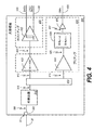
図4は、改良された光受信機の別の実施形態の回路図である。光受信機400は、光検出器310、信号ミラー410、プリアンプ420及びポストアンプ430の配列を備えている。この光受信機400は、光媒体20の第2の端部すなわち出力端部24で光信号を受け取り、接続体433でDATAと名付けられた第1の電気信号を発生する。この第1の電気信号は、入力302で受け取られた光データ信号の増幅されたバージョンである。接続体433上の第1の電気信号と接続体435上の相補信号は、論理ハイ電圧と論理ロー電圧との間に制限すなわちクランプされる。第1及び第2の電気信号に加えて、光受信機400は接続体429(OMAとラベル表示されている)上に、入力302における光変調振幅の大きさの電圧を発生する。
FIG. 4 is a circuit diagram of another embodiment of an improved optical receiver. The
光検出器310は、光結合機構305を介して入力302に接続されている。この光検出器310は、接続体315を介して信号ミラー410にさらに接続される。この光検出器310は、光−電気信号変換器である。すなわち、接続体315上の電流は、入力302及び光結合機構305を介して受け取られた時間変動する光信号に対応する。
The
信号ミラーすなわち電流ミラー410は、接続体413上に第1のプリアンプ用入力を、接続体415上に第2のプリアンプ用入力を提供する。この信号ミラー410は、回路の別の能動素子の電流を制御することによって、1つの能動素子を通して電流をコピーするように設計された回路である。信号ミラー410は、接続体413及び接続体415上の出力電流を、プリアンプ及びポストアンプの負荷(例えあるとしても)に関係なく一定に維持する。信号ミラー410は、光検出器310によって与えられた電流表示(representation)を接続体413及び接続体415上に提供する。
A signal or
接続体413上の第1のプリアンプ入力はトランスインピーダンス増幅器422に接続され、トランスインピーダンス増幅器422は接続体413上の電流を受け取り、この電流をプリアンプ出力接続体423上の時間変動する電圧に変換し、プリアンプ出力接続体423はポストアンプ430の単一入力に接続される。トランスインピーダンス増幅器422は動的に自動利得制御を用いて、プリアンプ420の出力における接続体423上の増幅された電圧が確実に、トランスインピーダンス増幅器422を飽和させることなく、入力302において時間変動する光信号スイングを正確に反映するようにする。
The first preamplifier input on
プリアンプ420内の光信号モニタリング経路は、固定利得増幅器424、低速回路426、及びドライバすなわちバッファ428の配列を備えている。固定利得増幅器424は、接続体415上で第2のプリアンプ入力を受け取り、時間変動する増幅された電圧を接続体425に転送する。この固定利得増幅器424は、光受信機400のダイナミックレンジにわたって制限されない、時間変動する増幅された電圧を提供するように構成される。低速回路は接続体425上の増幅された電圧を受け取り、平均ハイ信号レベルと平均ロー信号レベルの差を発生する。この平均ハイ信号レベルと平均ロー信号レベルの差は接続体427を経由して、接続体427に接続されたバッファ428に転送される。低速回路426は、kHzの範囲以下で動作する。バッファ428は、光受信機400の信号出力以外の場所にOMAの評価値を提供する。バッファ428はさらに、どのような外部モニタリング装置も接続体429上で確実にOMAの診断用評価値に悪影響を与えないようにする。
The optical signal monitoring path within the
信号制限ポストアンプ432は接続体423上で増幅された電圧を受け取り、DATAと名付けられた第1の電気信号を接続体433上に及びその相補信号(すなわち、第2の電気信号)を接続体435上に発生する。この方法では、ポストアンプ430は、入力302で受け取られた光信号に対する制限された、すなわちクランプされたバージョンを発生する。接続体433及び接続体435上の第1及び第2の電気信号は、それぞれ論理ハイ及び論理ローに対応する電圧レベルに制限すなわちクランプされる。
The
図5は、自動利得制御を使用する光受信機において、OMAの診断用評価値を提供する方法500を例示するフローチャートである。この方法500はブロック502で開始する。このブロック502では、光検出器の出力の表示が第1の信号レベルと第2の信号レベルとの間の差を測定する回路に与えられる。その後、ブロック504に示されているように、回路によって与えられた第1の信号レベルと第2の信号レベルとの間の差がバッファリングされる。このバッファリングされた第1の信号レベルと第2の信号レベルの差がOMAの診断用評価値である。
FIG. 5 is a flowchart illustrating a
図6は、自動利得制御を使用する光受信機において、OMAの診断用評価値を提供する方法600の実施形態を例示するフローチャートである。この方法600は、ブロック602で開始する。このブロック602では、光検出器の出力が、自動利得制御を用いるトランスインピーダンス増幅器に与えられる。ブロック604では、光受信機は、トランスインピーダンス増幅器の出力を第1の信号レベルと第2の信号レベルとの間の差を測定する回路に与えることによって、OMAの評価値を発生する。さらに、この回路は、トランスインピーダンス増幅器で使用された利得と第1の信号レベルと第2の信号レベルとの間の差の関数として、OMAの評価値を発生する。前述されたように、利得係数と差の積が、受信機の光検出器におけるOMAの評価値である。
FIG. 6 is a flowchart illustrating an embodiment of a
その後、ブロック606に示されているように、アナログ電圧で示されたOMAがバッファリングされる。ブロック608では、バッファリングされたOMA信号が、バッファに入力されたOMA信号を1つ以上のしきい値と比較する外部装置に接続される。ブロック610では、電圧レベルを絶対OMAに関連付けるキャリブレーション情報が提供される。
Thereafter, as shown in
図7は、自動利得制御を使用する光受信機において、OMAの診断用評価値を提供する方法700の別の実施形態のフローチャートである。この方法700は、ブロック702に示されるように開始する。このブロック702では、光受信機で受け取られた光に対応する電気信号が、第1及び第2の信号ミラー用出力信号を発生する信号ミラーに送られる。ブロック704では、第1の信号ミラー用出力信号の第1の表示が、光受信機のダイナミックレンジにわたって飽和されないようにする固定利得増幅器を用いて発生される。ブロック706では、第1の信号ミラーの第1の表示の中で、平均ハイ信号レベルと平均ロー信号レベルの差が測定される。この後で、ブロック708に示されているように、OMAの評価値が、平均ハイ信号レベルと平均ロー信号レベルの差をバッファリングすることによって発生される。ブロック710では、第2の信号ミラー用出力信号の第2の表示が、自動利得制御を使用するトランスインピーダンス増幅器を用いて発生される。ブロック712では、第2の表示を信号制限増幅器に与えることによって、電気信号に対応する差動出力信号が発生される。ブロック714では、OMAの評価値が1つ以上しきい値を使用する外部装置(すなわち、光受信機以外の装置)に接続されて、光通信リンクの品質の評価値を発生する。ブロック716では、OMAの評価値を光受信機における絶対OMAに関連付けるキャリブレーション情報が提供される。ブロック702〜712内のステップ又は機能の特定のシーケンスは、例証するために示されている。ブロック702〜712内のステップ又は機能の順序は、他の任意の適当な順序で実行できることに理解されたい。ブロック714及びブロック716のステップ又は機能は、選択自由である。
FIG. 7 is a flowchart of another embodiment of a
自動利得制御を使用する光受信機においてOMAの評価値を提供する光受信機のシステム及び方法に関する種々の実施形態が説明されたが、本開示内容の範囲に入るさらに多くの実施形態や具体例が考えられることは当業者には明らかであろう。従って、自動利得制御を使用する光受信機においてOMAの診断用評価値を提供する説明された光受信機のシステム及び方法は、添付された特許請求の範囲やそれらと等価なものに照らし合わせる場合を別にすれば、制限されたり限定されることはない。 While various embodiments of optical receiver systems and methods for providing OMA estimates in optical receivers using automatic gain control have been described, more embodiments and examples falling within the scope of this disclosure are described. It will be apparent to those skilled in the art that Accordingly, the described optical receiver system and method for providing diagnostic evaluation values for OMA in an optical receiver using automatic gain control is in light of the appended claims and their equivalents. Apart from that, there is no limit or limitation.
1 光通信システム
5、35 接続部
10 送信機
12 データ入力
14 光出力
20 光媒体
22 第1の端部
24 第2の端部
30 受信機
32 光入力
34 データ出力
300 光受信機
305 光結合機構
310 光検出器
315、323、325、333、335、337、339、413、415、425、427、429、433、435 接続体
320、420 プリアンプ
322、422 トランスインピーダンス増幅器
330、430 ポストアンプ
332、432 信号制限ポストアンプ
336、426 低速回路
338、428 バッファ
410 信号ミラー
423 プリアンプ出力接続体
424 固定利得増幅器
DESCRIPTION OF
Claims (12)
光検出器の出力の表示を、第1の平均信号レベルと第2の平均信号レベルとの間の差の絶対値を測定する回路に与えるステップと、
前記回路から受信された前記第1の平均信号レベルと前記第2の平均信号レベルとの間の前記差の絶対値をバッファリングするステップと、
を含む方法。 In an optical receiver using a transimpedance amplifier with automatic gain control, a method for providing a diagnostic evaluation value for optical modulation amplitude comprising:
Providing an indication of the output of the photodetector to a circuit for measuring an absolute value of the difference between the first average signal level and the second average signal level;
A step of buffering the absolute value of the difference between the received first average signal level and the second average signal level from the circuit,
Including methods.
前記トランスインピーダンス増幅器の入力、及び、前記信号ミラーと前記回路との間に挿入された固定利得増幅器の入力に、前記信号ミラーの第1の出力を与えるステップであって、前記固定利得増幅器が、前記光受信機のダイナミックレンジにわたって制限されない前記光検出器の出力の増幅された表示を提供する、前記信号ミラーの第1の出力を与えるステップと
を含む、請求項1に記載の方法。 Inserting a signal mirror at the output of the photodetector;
Providing a first output of the signal mirror to an input of the transimpedance amplifier and an input of a fixed gain amplifier inserted between the signal mirror and the circuit, the fixed gain amplifier comprising: Providing a first output of the signal mirror that provides an amplified display of the output of the photodetector that is not limited over the dynamic range of the optical receiver.
トランスインピーダンス増幅器入力において電流を受け取るように構成されると共に、増幅された電圧を発生するように構成されたトランスインピーダンス増幅器と、
前記増幅された電圧を受け取り、及び第1の平均信号レベルと該第1の平均信号レベルとは異なる第2の平均信号レベルとの間の差の絶対値を測定するように構成された回路であって、該回路が光変調振幅の診断用評価値を該回路の出力に提供する、回路と
を具備する光受信機システム。 An input coupled to the photodetector, the photodetector can it generate current in response to the optical signal of the input, and input,
A transimpedance amplifier with be configured to receive current, which is configured to generate an amplified voltage in the transimpedance amplifier circuit input,
Receiving said amplified voltage, and the first average signal level and the circuitry configured to measure the absolute value of the difference between the different second average signal level and the first average signal level a, the said circuit provides a diagnostic evaluation value of the optical modulation amplitude at the output of the circuit, an optical receiver system that includes a circuit with.
Applications Claiming Priority (2)
| Application Number | Priority Date | Filing Date | Title |
|---|---|---|---|
| US12/355,919 US8200100B2 (en) | 2009-01-19 | 2009-01-19 | Systems and methods for diagnostic monitoring of optical modulation amplitude at an optical receiver using automatic gain control |
| US12/355,919 | 2009-01-19 |
Publications (3)
| Publication Number | Publication Date |
|---|---|
| JP2010166567A JP2010166567A (en) | 2010-07-29 |
| JP2010166567A5 JP2010166567A5 (en) | 2012-07-19 |
| JP5345956B2 true JP5345956B2 (en) | 2013-11-20 |
Family
ID=42263114
Family Applications (1)
| Application Number | Title | Priority Date | Filing Date |
|---|---|---|---|
| JP2010008865A Active JP5345956B2 (en) | 2009-01-19 | 2010-01-19 | System and apparatus for diagnostic monitoring of optical modulation amplitude using automatic gain control in an optical receiver |
Country Status (3)
| Country | Link |
|---|---|
| US (2) | US8200100B2 (en) |
| JP (1) | JP5345956B2 (en) |
| DE (1) | DE102010000982B4 (en) |
Families Citing this family (12)
| Publication number | Priority date | Publication date | Assignee | Title |
|---|---|---|---|---|
| US20100150561A1 (en) * | 2008-12-12 | 2010-06-17 | Seung-Hyun Cho | Optical receiver, optical line terminal and method of recovering received signals |
| US8463137B2 (en) * | 2010-09-27 | 2013-06-11 | Titan Photonics, Inc. | System and method for transmissions via RF over glass |
| EP2833567B1 (en) * | 2012-03-27 | 2016-08-17 | Huawei Technologies Co., Ltd. | Optical fiber testing method, apparatus and passive optical network system |
| US8879909B2 (en) * | 2012-04-25 | 2014-11-04 | Source Photonics, Inc. | Circuits and methods for monitoring power parameters in an optical transceiver |
| US8901474B2 (en) | 2012-06-19 | 2014-12-02 | Source Photonics, Inc. | Enhanced received signal power indicators for optical receivers and transceivers, and methods of making and using the same |
| US9350447B1 (en) * | 2012-06-22 | 2016-05-24 | Adtran, Inc. | Systems and methods for protecting optical networks from rogue optical network terminals |
| US10564357B2 (en) | 2013-07-30 | 2020-02-18 | The Boeing Company | Plastic optical fiber bus network using tapered mixing rods |
| US11300730B2 (en) * | 2013-07-30 | 2022-04-12 | The Boeing Company | Plastic and glass optical fiber bus network having plural line replaceable units transmitting to a mixing rod |
| US9778419B1 (en) * | 2016-06-23 | 2017-10-03 | The Boeing Company | Fiber optical system with fiber end face area relationships |
| US11005573B2 (en) * | 2018-11-20 | 2021-05-11 | Macom Technology Solutions Holdings, Inc. | Optic signal receiver with dynamic control |
| US11658630B2 (en) | 2020-12-04 | 2023-05-23 | Macom Technology Solutions Holdings, Inc. | Single servo loop controlling an automatic gain control and current sourcing mechanism |
| WO2022200124A1 (en) * | 2021-03-26 | 2022-09-29 | Signify Holding B.V. | Method and apparatus for avoiding saturation in optical wireless point-to-point systems |
Family Cites Families (14)
| Publication number | Priority date | Publication date | Assignee | Title |
|---|---|---|---|---|
| GB8728853D0 (en) * | 1987-12-10 | 1988-01-27 | Bt & D Technologies Ltd | Transimpedance pre-amplifier & receiver including pre-amplifier |
| US5402433A (en) | 1994-01-05 | 1995-03-28 | Alcatel Network Systems, Inc. | Apparatus and method for laser bias and modulation control |
| JP2004056150A (en) * | 2002-07-19 | 2004-02-19 | Matsushita Electric Ind Co Ltd | Method and program for controlling lma and er of laser diode generating burst signal, laser diode drive circuit, integrated circuit, transmitter and communications system |
| US7539423B2 (en) * | 2003-01-10 | 2009-05-26 | Avago Technologies Fiber Ip (Singapore) Pte. Ltd. | Loss of signal detection and programmable behavior after error detection |
| US6891866B2 (en) * | 2003-01-10 | 2005-05-10 | Agilent Technologies, Inc. | Calibration of laser systems |
| US6922231B1 (en) | 2003-01-23 | 2005-07-26 | Opnext, Inc. | Receiver optical sub-assembly with diagnostic signal |
| US7463674B2 (en) | 2003-04-09 | 2008-12-09 | Avago Technologies Fiber Ip (Singapore) Pte. Ltd. | Tables for determining the signal strength of a received signal in a fibre optics transceiver |
| US7045752B2 (en) | 2003-06-30 | 2006-05-16 | Intel Corporation | Illuminated and non-illuminated photodiodes for monitoring and controlling AC and DC components of a laser beam |
| US7853149B2 (en) * | 2005-03-08 | 2010-12-14 | Clariphy Communications, Inc. | Transmitter frequency peaking for optical fiber channels |
| US7199666B2 (en) * | 2005-03-10 | 2007-04-03 | Avago Technologies Fiber Ip (Singapore) Pte. Ltd. | Construction and use of preamps having discrete gain states |
| US7826739B2 (en) | 2006-09-14 | 2010-11-02 | Finisar Corporation | Determination and adjustment of laser modulation current in an optical transmitter |
| JP2008135974A (en) * | 2006-11-28 | 2008-06-12 | Sumitomo Electric Ind Ltd | Optical receiving circuit |
| JP4704367B2 (en) * | 2007-01-18 | 2011-06-15 | 富士通テレコムネットワークス株式会社 | Optical wavelength division multiplexing equipment |
| US20080226288A1 (en) | 2007-03-14 | 2008-09-18 | Miller Frederick W | Method and apparatus for performing receiver sensitivity testing and stressed receive sensitivity testing in a transceiver |
-
2009
- 2009-01-19 US US12/355,919 patent/US8200100B2/en active Active
-
2010
- 2010-01-18 DE DE102010000982.2A patent/DE102010000982B4/en active Active
- 2010-01-19 JP JP2010008865A patent/JP5345956B2/en active Active
-
2012
- 2012-05-11 US US13/469,179 patent/US8346101B2/en active Active
Also Published As
| Publication number | Publication date |
|---|---|
| DE102010000982B4 (en) | 2020-01-02 |
| US8200100B2 (en) | 2012-06-12 |
| JP2010166567A (en) | 2010-07-29 |
| US20100183296A1 (en) | 2010-07-22 |
| US8346101B2 (en) | 2013-01-01 |
| US20120219286A1 (en) | 2012-08-30 |
| DE102010000982A8 (en) | 2010-11-11 |
| DE102010000982A1 (en) | 2010-07-22 |
Similar Documents
| Publication | Publication Date | Title |
|---|---|---|
| JP5345956B2 (en) | System and apparatus for diagnostic monitoring of optical modulation amplitude using automatic gain control in an optical receiver | |
| US7147387B2 (en) | Transmitter preemphasis in fiber optic links | |
| JP4465010B2 (en) | System and method for providing diagnostic information using an EDC transceiver | |
| US7680421B2 (en) | Multimode optical fibre communication system | |
| US6738584B1 (en) | Method for optical fiber communication, and terminal device and system for use in carrying out the method | |
| ES2245469T3 (en) | OPTICAL TRANSMISSION PROCEDURE AND SYSTEM TO COMPENSATE DISPERSION IN OPTICAL TRANSMISSION TRAJECTS. | |
| US8901474B2 (en) | Enhanced received signal power indicators for optical receivers and transceivers, and methods of making and using the same | |
| JP4876735B2 (en) | Optical pulse tester | |
| US7945159B2 (en) | Diagnostic method and diagnostic chip for determining the bandwidth of optical fibers | |
| US9172209B2 (en) | Resistive heating element for enabling laser operation | |
| KR20000077077A (en) | Optical transmitter/receiver and method of optical transmission and reception | |
| JP2008042493A (en) | Optical receiving circuit and its identification level control method | |
| JP2007173908A (en) | Burst optical signal receiver and gain setting method thereof | |
| Atef et al. | An integrated optical receiver for multilevel data communication over large core step index plastic optical fiber | |
| KR20110067777A (en) | Optical transmitting/receiving control apparatus | |
| JP2008218897A (en) | Optical signal transmitter, output control circuit and output control method | |
| Sun et al. | Transmission of 28-Gb/s duobinary signals over 45-km SSMF Using 1.55-µm directly modulated laser | |
| JP2009168833A (en) | Bias circuit of external modulator | |
| JP2008141498A (en) | Optical transmitter | |
| CN217276797U (en) | Optical fiber time delay measuring device | |
| Atef et al. | An optical receiver for eight-level data communication over step index plastic optical fiber | |
| US7319820B2 (en) | Method of manufacturing optical communication system | |
| CN114088346A (en) | Optical fiber time delay measuring device | |
| JP4957567B2 (en) | Optical receiver | |
| JP4069036B2 (en) | Mark rate evaluation system |
Legal Events
| Date | Code | Title | Description |
|---|---|---|---|
| RD03 | Notification of appointment of power of attorney |
Free format text: JAPANESE INTERMEDIATE CODE: A7423 Effective date: 20110711 |
|
| A521 | Request for written amendment filed |
Free format text: JAPANESE INTERMEDIATE CODE: A523 Effective date: 20120605 |
|
| A621 | Written request for application examination |
Free format text: JAPANESE INTERMEDIATE CODE: A621 Effective date: 20120605 |
|
| A711 | Notification of change in applicant |
Free format text: JAPANESE INTERMEDIATE CODE: A712 Effective date: 20130718 |
|
| A977 | Report on retrieval |
Free format text: JAPANESE INTERMEDIATE CODE: A971007 Effective date: 20130731 |
|
| TRDD | Decision of grant or rejection written | ||
| A01 | Written decision to grant a patent or to grant a registration (utility model) |
Free format text: JAPANESE INTERMEDIATE CODE: A01 Effective date: 20130813 |
|
| A61 | First payment of annual fees (during grant procedure) |
Free format text: JAPANESE INTERMEDIATE CODE: A61 Effective date: 20130815 |
|
| R150 | Certificate of patent or registration of utility model |
Ref document number: 5345956 Country of ref document: JP Free format text: JAPANESE INTERMEDIATE CODE: R150 Free format text: JAPANESE INTERMEDIATE CODE: R150 |
|
| R250 | Receipt of annual fees |
Free format text: JAPANESE INTERMEDIATE CODE: R250 |
|
| R250 | Receipt of annual fees |
Free format text: JAPANESE INTERMEDIATE CODE: R250 |
|
| R250 | Receipt of annual fees |
Free format text: JAPANESE INTERMEDIATE CODE: R250 |
|
| S111 | Request for change of ownership or part of ownership |
Free format text: JAPANESE INTERMEDIATE CODE: R313111 |
|
| R350 | Written notification of registration of transfer |
Free format text: JAPANESE INTERMEDIATE CODE: R350 |
|
| R250 | Receipt of annual fees |
Free format text: JAPANESE INTERMEDIATE CODE: R250 |
|
| R250 | Receipt of annual fees |
Free format text: JAPANESE INTERMEDIATE CODE: R250 |
|
| R250 | Receipt of annual fees |
Free format text: JAPANESE INTERMEDIATE CODE: R250 |
|
| R250 | Receipt of annual fees |
Free format text: JAPANESE INTERMEDIATE CODE: R250 |
|
| R250 | Receipt of annual fees |
Free format text: JAPANESE INTERMEDIATE CODE: R250 |