JP5343727B2 - Digital camera device - Google Patents
Digital camera device Download PDFInfo
- Publication number
- JP5343727B2 JP5343727B2 JP2009146500A JP2009146500A JP5343727B2 JP 5343727 B2 JP5343727 B2 JP 5343727B2 JP 2009146500 A JP2009146500 A JP 2009146500A JP 2009146500 A JP2009146500 A JP 2009146500A JP 5343727 B2 JP5343727 B2 JP 5343727B2
- Authority
- JP
- Japan
- Prior art keywords
- signal processing
- analog signal
- ccd
- shutter key
- digital camera
- Prior art date
- Legal status (The legal status is an assumption and is not a legal conclusion. Google has not performed a legal analysis and makes no representation as to the accuracy of the status listed.)
- Expired - Fee Related
Links
Images


Classifications
-
- H—ELECTRICITY
- H04—ELECTRIC COMMUNICATION TECHNIQUE
- H04N—PICTORIAL COMMUNICATION, e.g. TELEVISION
- H04N23/00—Cameras or camera modules comprising electronic image sensors; Control thereof
- H04N23/60—Control of cameras or camera modules
- H04N23/65—Control of camera operation in relation to power supply
- H04N23/651—Control of camera operation in relation to power supply for reducing power consumption by affecting camera operations, e.g. sleep mode, hibernation mode or power off of selective parts of the camera
-
- H—ELECTRICITY
- H04—ELECTRIC COMMUNICATION TECHNIQUE
- H04N—PICTORIAL COMMUNICATION, e.g. TELEVISION
- H04N23/00—Cameras or camera modules comprising electronic image sensors; Control thereof
- H04N23/60—Control of cameras or camera modules
- H04N23/667—Camera operation mode switching, e.g. between still and video, sport and normal or high- and low-resolution modes
-
- H—ELECTRICITY
- H04—ELECTRIC COMMUNICATION TECHNIQUE
- H04N—PICTORIAL COMMUNICATION, e.g. TELEVISION
- H04N23/00—Cameras or camera modules comprising electronic image sensors; Control thereof
- H04N23/60—Control of cameras or camera modules
- H04N23/67—Focus control based on electronic image sensor signals
- H04N23/673—Focus control based on electronic image sensor signals based on contrast or high frequency components of image signals, e.g. hill climbing method
-
- H—ELECTRICITY
- H04—ELECTRIC COMMUNICATION TECHNIQUE
- H04N—PICTORIAL COMMUNICATION, e.g. TELEVISION
- H04N25/00—Circuitry of solid-state image sensors [SSIS]; Control thereof
- H04N25/40—Extracting pixel data from image sensors by controlling scanning circuits, e.g. by modifying the number of pixels sampled or to be sampled
- H04N25/42—Extracting pixel data from image sensors by controlling scanning circuits, e.g. by modifying the number of pixels sampled or to be sampled by switching between different modes of operation using different resolutions or aspect ratios, e.g. switching between interlaced and non-interlaced mode
-
- H—ELECTRICITY
- H04—ELECTRIC COMMUNICATION TECHNIQUE
- H04N—PICTORIAL COMMUNICATION, e.g. TELEVISION
- H04N25/00—Circuitry of solid-state image sensors [SSIS]; Control thereof
- H04N25/40—Extracting pixel data from image sensors by controlling scanning circuits, e.g. by modifying the number of pixels sampled or to be sampled
- H04N25/44—Extracting pixel data from image sensors by controlling scanning circuits, e.g. by modifying the number of pixels sampled or to be sampled by partially reading an SSIS array
- H04N25/445—Extracting pixel data from image sensors by controlling scanning circuits, e.g. by modifying the number of pixels sampled or to be sampled by partially reading an SSIS array by skipping some contiguous pixels within the read portion of the array
-
- H—ELECTRICITY
- H04—ELECTRIC COMMUNICATION TECHNIQUE
- H04N—PICTORIAL COMMUNICATION, e.g. TELEVISION
- H04N25/00—Circuitry of solid-state image sensors [SSIS]; Control thereof
- H04N25/50—Control of the SSIS exposure
- H04N25/53—Control of the integration time
Abstract
Description
本発明は、CCD等の電荷転送型の固体撮像素子を備えたデジタルカメラ装置に関するものである。 The present invention relates to a digital camera apparatus provided with a charge transfer type solid-state imaging device such as a CCD.
従来、撮像装置の消費電力を削減するための技術として以下の技術が提案されている。例えば下記の特許文献1には、撮像装置に、撮像素子を駆動しているときのブランキング期間中には、相関二重サンプリング処理のためのサンプルホールドのタイミングを示すタイミング信号を停止させて、ブランキング期間中に相関二重サンプリング処理を停止させる動作を行わせる技術が提案されている。また、下記の特許文献2には、撮像装置に、長時間露光が行われた場合、長時間露光により得られた撮像信号が固体撮像素子から出力されるまでの期間は、CDSとPGAとアナログデジタル変換回路とからなるAFEを停止させる動作を行わせる技術が提案されている。さらに、下記の特許文献3には、撮像装置に、画像をくり返し撮像する際に、画像信号の読み出し期間以外の期間中は、AFEを停止させる動作を行わせる技術が提案されている。
Conventionally, the following techniques have been proposed as techniques for reducing the power consumption of an imaging apparatus. For example, in Patent Document 1 below, the timing signal indicating the timing of the sample hold for the correlated double sampling process is stopped during the blanking period when the imaging device is driven in the imaging device, A technique for performing an operation of stopping the correlated double sampling process during the blanking period has been proposed. Further, in
しかしながら、上記の各技術によれば撮像期間中における撮像装置の消費電力を削減することができるが、上記の各技術をデジタルカメラ装置に採用したとしても、ユーザによって撮影操作が行われている間における消費電力の削減効果が未だ十分とはいえないという問題があった。 However, according to each of the above technologies, the power consumption of the imaging device during the imaging period can be reduced. However, even if each of the above technologies is adopted in the digital camera device, the user can perform a shooting operation. There has been a problem that the effect of reducing the power consumption is still not sufficient.
本発明は、かかる従来の課題に鑑みてなされたものであり、デジタルカメラ装置において、撮影操作が行われている間の消費電力を従来に比べ一層削減することを目的とする。 The present invention has been made in view of such a conventional problem, and an object of the present invention is to further reduce power consumption during a photographing operation in a digital camera device as compared with the conventional art.
本発明の第1の観点に係るデジタルカメラ装置にあっては、被写体像を光電変換することによって、被写体像を表すアナログ信号を出力する固体撮像素子と、前記固体撮像素子から出力されるアナログ信号に対してアナログ信号処理を施す信号処理手段と、半押しと全押しの2段階での操作が可能なシャッターキーと、前記シャッターキーが押されていない時に、前記信号処理手段によるアナログ信号処理後の信号からなる画像情報を、ライブビュー画像として表示手段に表示させる表示制御手段と、前記シャッターキーが半押しされた時に、前記信号処理手段によるアナログ信号処理後の信号からなる画像情報に基づき、被写体にピントを合わせるためのフォーカス制御を行うフォーカス制御手段と、前記シャッターキーが全押しされた時に、前記信号処理手段によるアナログ信号処理後の信号からなる画像情報を記録媒体に保存するための記録制御を行う記録制御手段と、前記シャッターキーが押されていない時を除いて、前記シャッターキーが半押し又は全押しされた時の前記フォーカス制御又は前記記録制御の最中における、画素情報として使用されない所定の電荷からなるアナログ信号が、画素情報として使用される電荷からなるアナログ信号よりも高速に前記固体撮像素子から掃き出される高速掃き出し期間中に、前記信号処理手段によるアナログ信号処理を停止させる停止制御手段とを備えたことを特徴とする。 In the digital camera device according to the first aspect of the present invention, a solid-state image sensor that outputs an analog signal representing a subject image by photoelectrically converting the subject image, and an analog signal output from the solid-state image sensor. Signal processing means for performing analog signal processing on the shutter, a shutter key that can be operated in two steps of half-pressing and full-pressing, and after analog signal processing by the signal processing means when the shutter key is not pressed Based on the image information consisting of the signal after the analog signal processing by the signal processing means when the shutter key is pressed halfway, the display control means for displaying the image information consisting of the signal of the signal on the display means as a live view image, Focus control means that performs focus control to focus on the subject and when the shutter key is fully pressed A recording control means for performing recording control for storing image information consisting of signals after analog signal processing by the signal processing means, and the shutter key except when the shutter key is not pressed. During the focus control or the recording control when half-pressed or fully pressed, an analog signal composed of a predetermined charge not used as pixel information is faster than an analog signal composed of a charge used as pixel information. wherein in the solid state imaging device fast swept out from the sweep-out period, characterized by comprising a stop control means for stopping the analog signal processing by the signal processing means.
本発明の第2の観点に係るプログラムにあっては、被写体像を光電変換することによって、被写体像を表すアナログ信号を出力する固体撮像素子と、前記固体撮像素子から出力されるアナログ信号に対してアナログ信号処理を施す信号処理手段と、半押しと全押しの2段階での操作が可能なシャッターキーとを備えたデジタルカメラ装置が有するコンピュータを、前記シャッターキーが押されていない時に、前記信号処理手段によるアナログ信号処理後の信号からなる画像情報を、ライブビュー画像として表示手段に表示させる表示制御手段、前記シャッターキーが半押しされた時に、前記信号処理手段によるアナログ信号処理後の信号からなる画像情報に基づき、被写体にピントを合わせるためのフォーカス制御を行うフォーカス制御手段、前記シャッターキーが全押しされた時に、前記信号処理手段によるアナログ信号処理後の信号からなる画像情報を記録媒体に保存するための記録制御を行う記録制御手段、前記シャッターキーが押されていない時を除いて、前記シャッターキーが半押し又は全押しされた時の前記フォーカス制御又は前記記録制御の最中における、画素情報として使用されない所定の電荷からなるアナログ信号が、画素情報として使用される電荷からなるアナログ信号よりも高速に前記固体撮像素子から掃き出される高速掃き出し期間中に、前記信号処理手段によるアナログ信号処理を停止させる停止制御手段として機能させることを特徴とする。 In the program according to the second aspect of the present invention, a solid-state image sensor that outputs an analog signal representing a subject image by photoelectrically converting the subject image, and an analog signal output from the solid-state image sensor. A digital camera device having a signal processing means for performing analog signal processing and a shutter key that can be operated in two steps of half-pressing and full-pressing , when the shutter key is not pressed, Display control means for displaying image information consisting of signals after analog signal processing by the signal processing means on the display means as a live view image, and signals after analog signal processing by the signal processing means when the shutter key is half-pressed Focus control means for performing focus control for focusing on a subject based on image information consisting of Recording control means for performing recording control for storing image information consisting of signals after analog signal processing by the signal processing means in a recording medium when the shutter key is fully pressed, and when the shutter key is not pressed Except that the analog signal consisting of a predetermined charge not used as pixel information during the focus control or the recording control when the shutter key is half-pressed or fully pressed is a charge used as pixel information. during high-speed sweep period are swept from the solid-state imaging device in higher speed than the analog signal consisting, characterized in that to function as stop control means for stopping the analog signal processing by the signal processing means.
本発明によれば、デジタルカメラ装置において、撮影操作が行われている間の消費電力を従来に比べ一層削減することが可能となる。 According to the present invention, in the digital camera device, it is possible to further reduce the power consumption during the shooting operation as compared with the related art.
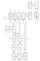
以下、本発明を適用した実施形態について、図を参照しながら説明する。図1は、本発明の実施形態として例示するデジタルカメラ装置1のハードウェア構成の概略を示すブロック図である。 Embodiments to which the present invention is applied will be described below with reference to the drawings. FIG. 1 is a block diagram showing an outline of a hardware configuration of a digital camera device 1 exemplified as an embodiment of the present invention.
デジタルカメラ装置1は、CPU(Central Processing Unit)2によってシステムの全体を制御される構成である。デジタルカメラ装置1は、フォーカスレンズを含む光学系とメカニカルシャッターからなるレンズブロック3と、レンズブロック3内における光学系、メカニカルシャッターをそれぞれ駆動するためのモータ等のアクチュエータ4とを有している。そして、アクチュエータ4を駆動するための各種のドライバにより構成されるドライバブロック5がバス6を介して接続されている。
The digital camera device 1 has a configuration in which the entire system is controlled by a CPU (Central Processing Unit) 2. The digital camera device 1 includes a
また、デジタルカメラ装置1は、被写体を撮像するための固体撮像素子としてCCD(Charge Coupled Device)7を有している。CCD7は公知の電荷転送型の固体撮像素子であり、図示しないが、水平及び垂直方向に多数配置されて各々が画素を構成する多数のフォトダイオードが設けられるとともに、フォトダイオードの各列に複数の垂直転送CCDの列が隣接し、最後の行の垂直転送CCDに隣接して水平転送CCDが1本設けられた構造である。
The digital camera device 1 also has a CCD (Charge Coupled Device) 7 as a solid-state imaging device for imaging a subject. The
ドライバ8は、TG(Timing Generator)9が生成した垂直CCD駆動タイミング信号と、水平CCD駆動タイミング信号と、電子シャッタタイミング信号とに従い、CCD駆動信号を生成する。そして、ドライバ8は、生成したCCD駆動信号をCCD7へ供給してCCD7を駆動する。
The driver 8 generates a CCD drive signal according to a vertical CCD drive timing signal, a horizontal CCD drive timing signal, and an electronic shutter timing signal generated by a TG (Timing Generator) 9. Then, the driver 8 supplies the generated CCD drive signal to the
TG9は、上記の垂直CCD駆動タイミング信号と、水平CCD駆動タイミング信号と、電子シャッタタイミング信号とからなる駆動タイミング信号を、CPU2により設定された駆動モードに応じて生成する。CCD7の駆動モードは、ドラフトモードとAFモードとキャプチャーモードとの3種類である。TG9は、CCD7の駆動モードの種類を示す設定値を記憶するレジスタを内部に有しており、上記設定値がCPU2により設定されることにより、各々の駆動モードに応じた上記の駆動タイミング信号(垂直CCD駆動タイミング信号、水平CCD駆動タイミング信号、電子シャッタタイミング信号)を生成する。
The TG 9 generates a drive timing signal composed of the vertical CCD drive timing signal, the horizontal CCD drive timing signal, and the electronic shutter timing signal according to the drive mode set by the
CCD7は、ドライバ8によって駆動されることにより、レンズブロック3の光学系において結像された被写体の光学像(被写体像)を光電変換することによって、被写体像を表すアナログの撮像信号をAFE(Analog Front End)10に供給する。
The
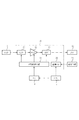
図2は、AFE10の構成を示した図である。AFE10は、CDS(Correlated Double Sampling)51と、PGA(Programmable Gain Amp)52、ADC(Analog-to-Digital converter)53、AFE制御回路54、給電スイッチ55から構成され、信号処理手段として機能する。
FIG. 2 is a diagram illustrating the configuration of the
CDS51は、CCD7から供給されたアナログの撮像信号に含まれるノイズを相関二重サンプリングによって除去し、ノイズ除去後の撮像信号をPGA52へ供給する。PGA52は、ノイズ除去後の撮像信号を増幅し、増幅後の撮像信号をADC53へ供給する。ADC53は、増幅後の撮像信号をデジタルの撮像信号に変換し、変換後のデジタル撮像信号をDSP(Digital Signal Processor)11へ出力する。CDS51による撮像信号からのノイズ除去と、PGA52による撮像信号の増幅と、ADC53による撮像信号のデジタル変換とからなる一連の信号処理がAFE10のアナログ信号処理である。
The
AFE制御回路54は、TG9から供給されるAFE駆動信号を受け取る。AFE駆動信号とは、AFE10におけるアナログ信号処理の処理タイミングを規定する信号である。AFE制御回路54は、AFE駆動信号が示すタイミングでCDS51とPGA52とADC53との各アナログ回路の駆動を制御する。給電スイッチ55は、電源回路18から上記の各アナログ回路へ供給される駆動電流を、CPU2から供給される駆動開始信号および駆動停止信号に従いオン・オフ制御する。各アナログ回路へ供給される駆動電流は、各アナログ回路を駆動するための電流である。
The
DSP11は、入力した撮像信号に対しペデスタルクランプ等の処理を施してRGBデータに変換し、さらにRGBデータを輝度(Y)成分及び色差(UV)成分からなるYUVデータに変換する。また、DSP11は、YUVデータにオートホワイトバランス、輪郭強調、画素補間などの画品質向上のためのデジタル信号処理を施し、順次SDRAM12に記憶させる。
The DSP 11 performs processing such as pedestal clamping on the input imaging signal to convert it into RGB data, and further converts the RGB data into YUV data composed of a luminance (Y) component and a color difference (UV) component. Further, the DSP 11 performs digital signal processing for improving image quality such as auto white balance, contour emphasis, and pixel interpolation on the YUV data, and sequentially stores them in the
撮影用の記録モードでは、SDRAM12に1フレーム分(1画面分)のYUVデータ(画像データ)が蓄積される毎に、YUVデータが液晶モニタ13へ送られてライブビュー画像として画面表示される。また、シャッターキーが押された撮影時には、CPU2がSDRAM12に一時記憶されるYUVデータを圧縮し、所定のフォーマットの画像ファイルとして外部メモリ14に記録する。外部メモリ14は、図示しないカードインターフェイスを介してカメラ本体に接続された着脱自在なメモリカードである。
In the recording mode for shooting, whenever one frame (one screen) of YUV data (image data) is stored in the
再生モードにおいてCPU2は、外部メモリ14に記録された画像ファイルをユーザの選択操作に応じて読み出して伸張し、YUVデータとしてSDRAM12に展開させた後、液晶モニタ13に表示させる。
CPU2 in the reproduction mode, extends reads in accordance with image files recorded in the
フラッシュメモリ15は、CPU2にカメラ全体を制御させるための複数種のプログラムやデータが記憶されているプログラム格納用メモリである。フラッシュメモリ15に記憶されているプログラムには、レンズブロック3の光学系を、公知のコントラスト検出方式によって被写体にピントが合うフォーカス位置へ自動制御するAF(auto focus)制御を行うためのAF制御プログラムが含まれる。
The
CPU2によるAF制御は、画角内の中央部分に存在する被写体にピントを合わせる中央重点方式である。AF制御に際してCPU2は、レンズブロック3の光学系を移動させながら、CCD2の有効画素領域101における予め決められている中央部分102(図4参照)に相当する画像データにおけるコントラストを逐次検出し、コントラストが最大となる位置、つまりフォーカス位置に光学系を移動させるものである。
The AF control by the
一方、CPU2にはサブCPU16が接続されている。サブCPU16には電源ボタンや撮影を指示するためのシャッターキー、ズーム操作ボタン、モード切替キー等のスイッチ類から構成されるキー入力部17と電源回路18が接続されている。キー入力部17におけるシャッターキーは、半押し操作(ハーフシャッター)と全押し操作との2段階操作が可能な所謂ハーフシャッター機能を備えたものであり、記録モードではシャッターキーの半押し操作がCPU2によるAF制御の開始トリガとなる。
On the other hand, a
サブCPU16は、キー入力部17におけるスイッチ類の操作状態を定常的にスキャンし、ユーザによるスイッチ操作の内容に応じた操作信号をCPU2へ送る。電源回路18は、カメラ本体に収容されたバッテリ19を電源として、デジタルカメラ装置1の基準電圧、及び前述した各部が必要とする電圧を生成し各部に供給する。
The
図3は、デジタルカメラ装置1に記録モードが設定されているとき、CPU2が、フラッシュメモリ15に記憶されている前述したプログラムに基づき動作することにより実現される機能の一部を示した機能ブロック図である。記録モードにおいてCPU2は、停止制御部2a、駆動モード設定部2b、AF制御部2c、撮影処理部2dとして機能する。そして、記録モードにおいては停止制御部2aが必要に応じて前述したAFE10の動作を停止させる。また、駆動モード設定部2bが、デジタルカメラ装置1の動作に応じてCCD7の駆動モードを設定し、設定した駆動モードに応じた駆動タイミング信号をTG9に生成させる。また、AF制御部2cが、ドライバブロック5を制御することによりレンズブロック3の光学系を移動させる。また、撮影処理部2dが、デジタルカメラ装置1における上記以外の種々の動作を制御する。
FIG. 3 is a functional block diagram showing a part of functions realized by the
ここで、前述したCCD7の駆動モードについて説明する。CCD7の駆動モードは、ドラフトモードとAFモードとキャプチャーモードとの3種類である。
Here, the drive mode of the
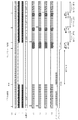
ドラフトモードは、液晶モニタ13がライブビュー画像を表示している間に設定される駆動モードである。図5は、ドラフトモードにおいてドライバ8が出力するCCD駆動信号を示したタイミングチャートである。垂直同期信号VDは、1画面周期のタイミング信号、つまりCCD7に蓄積された1フレーム分の電荷の読み出し開始タイミングを示す信号である。水平同期信号HDは、1ライン周期のタイミング信号、つまりCCD7に蓄積された1ライン分の電荷の読み出し開始タイミングを示す信号である。ここで、1ラインとは、CCD7において水平及び垂直方向に配置されているフォトダイオードが並ぶ水平方向の各々の行(水平方向に連なる一列分の画素)である。
The draft mode is a drive mode that is set while the liquid crystal monitor 13 displays a live view image. FIG. 5 is a timing chart showing CCD drive signals output from the driver 8 in the draft mode. The vertical synchronization signal VD is a timing signal for one screen cycle, that is, a signal indicating the readout start timing of charges for one frame accumulated in the
ドライバ8は、図5に示したように、垂直同期信号VDの出力間隔である1画面周期において、電荷の垂直転送用の電圧を印加するための電極数(ここでは4電極)に応じた4相の垂直CCD駆動パルスV1〜V4と、電荷の水平転送用の電圧を印加するための電極数(ここでは2電極)に応じた2相の水平CCD駆動パルスH1,H2と、電子シャッタパルスSUBを出力する。 As shown in FIG. 5, the driver 8 has 4 corresponding to the number of electrodes (four electrodes in this case) for applying a voltage for vertical transfer of charges in one screen cycle that is an output interval of the vertical synchronization signal VD. Two-phase horizontal CCD drive pulses H1 and H2 according to the number of phases of vertical CCD drive pulses V1 to V4, the number of electrodes (two electrodes in this case) for applying a horizontal transfer voltage, and an electronic shutter pulse SUB Is output.
CCD7のフォトダイオードに蓄積された各画素の電荷は、1画面周期内において、垂直同期信号VDの立ち上がり直後の電荷読み出し期間(図5で「電荷読み出し」)に垂直転送CCDへ転送される。さらに、水平同期信号HDの出力間隔である1ライン周期毎に、垂直CCD駆動パルスV1〜V4によって、垂直転送CCD(転送経路)へ転送された各ラインの電荷が水平転送CCD(水平転送路)へ順に垂直転送されて、1ライン分の電荷が水平転送CCDへ転送される。そして、水平転送CCDへ転送された1ライン分の電荷が、水平CCD駆動パルスH1,H2に同期して順にCCD7から出力される。また、ドライバ8は、垂直CCD駆動パルスV1〜V4を出力する期間、水平CCD駆動パルスH1,H2の出力を停止する。水平CCD駆動パルスH1,H2が停止している期間(図5で「HB」)はHブランキング期間と呼ばれる。 Charge of each pixel stored in the photodiode of CCD7, in one screen period, are transferred to the charge readout period immediately after the rise of the vertical synchronizing signal VD ( "charge readout" in FIG. 5) to the vertical transfer CCD. Further, for each line period which is the output interval of the horizontal synchronizing signal HD, the vertical CCD driving pulses V1-V4, the charge of the respective lines are transferred to the vertical transfer CCD (transfer path) horizontal transfer CCD (horizontal transfer path) It is sequentially vertically transferred to the charge of one line is transferred to the horizontal transfer CCD. The charge for one line transferred to the horizontal transfer CCD is output from the CCD7 sequentially in synchronism with the horizontal CCD drive pulse H1, H2. Further, the driver 8 stops outputting the horizontal CCD drive pulses H1 and H2 during a period in which the vertical CCD drive pulses V1 to V4 are output. The period during which the horizontal CCD drive pulses H1 and H2 are stopped (“HB” in FIG. 5) is called an H blanking period.
そして、1画面周期にCCD7の全画素分(1フレーム分)の電荷が撮像信号として出力され、複数ライン分の蓄積電荷の画素データ、つまり図5に示した有効データに基づきライブビュー画像が生成される。なお、1画面周期はCCD7の全画素分の蓄積電荷の出力にかかる時間よりも長く設定されており、全画面分の蓄積電荷が出力し終わるとCCD7からは無効な蓄積電荷が出力される。この無効な蓄積電荷が出力される期間(図5で「Vブランキング」)は、一般にVブランキング期間と呼ばれる。
Then, the charge for all pixels (one frame) of the
また、前述したAFモードは、CPU2がAF制御を行っているAF制御期間、より具体的にはユーザによりシャッターキーの半押し操作が行われた直後から、レンズブロック3の光学系がフォーカス位置に移動するまでの期間に設定される駆動モードである。図6は、ドライバ8が、CCD7をAFモードで駆動している間の1画面周期内に出力するCCD駆動信号を示したタイミングチャートである。
In the AF mode described above, the optical system of the
前述したようにCPU2によるAF制御はコントラスト検出方式で、かつ中央重点方式であるため、画面の中央部分の画素データのみがAF制御に必要であり、中央部分を除く他の部分の画素データはAF制御に不要である。そのためAFモードでの1画面周期内においてドライバ8は、図4に示したCCD7の有効画素領域101の中央部分102の上側の上側画素領域101aと、中央部分102の下側の下側画素領域101cとに配置されているフォトダイオードの蓄積電荷を掃き捨てる。そして、上側画素領域101aと下側画素領域101cとに挟まれた中央部分102を含む中間画素領域101bに配置されているフォトダイオードの蓄積電荷のみをCCD7から出力させる。
As described above, since the AF control by the
すなわち1画面周期内にドライバ8は、図4に示したCCD7の有効画素領域101の上側画素領域101aと下側画素領域101cの蓄積電荷を読み出す複数ライン分のライン周期内に、垂直CCD駆動パルスV1〜V4と水平CCD駆動パルスH1,H2を同時に出力する高速掃き出し駆動という駆動を行う。すなわちドライバ8は、上側画素領域101aと下側画素領域101cをそれぞれ構成する複数ライン分の蓄積電荷をフォトダイオードから垂直転送CCDに転送した後、一気に垂直転送して水平転送CCDに送る。さらに、ドライバ8は、水平転送CCDに溜まった(加算された)複数ライン分の電荷を一気に水平転送して掃き出させる。
That is, within one screen period, the driver 8 performs vertical CCD drive pulses within a line period for a plurality of lines for reading out the accumulated charges in the
ドライバ8が高速掃き出し駆動を行う期間が図6に示した高速掃き出し期間である。すなわち高速掃き出し期間は、CCD7の有効画素領域101の上側画素領域101aと下側画素領域101cとにおける、AF制御において画素情報として使用されない所定の画素の電荷を、CCD7の有効画素領域101の中間画素領域101bにおけるAF制御において画素情報として使用される画素よりも高速で掃き出させる駆動期間である。
The period during which the driver 8 performs high-speed sweep driving is the high-speed sweep period shown in FIG. That is, in the high-speed sweep period, the charge of a predetermined pixel that is not used as pixel information in the AF control in the
また、ドライバ8は、高速掃き出し期間を除く、図4に示したCCD7の有効画素領域101の中間画素領域101bに対応する複数ライン分のライン周期、つまり図6に示した有効データ掃き出し期間には、ドラフトモードの場合と同様の垂直CCD駆動パルスV1〜V4と水平CCD駆動パルスH1,H2とを出力する。そして、ドライバ8は、CCD7の有効画素領域101の中間画素領域101bの連続する複数ライン分の蓄積電荷、すなわちフォーカス制御時に画素情報として使用される画素の電荷を1ライン分ずつ水平転送CCDに垂直転送した後、1ライン毎に水平転送して水平転送CCDから掃き出させる。
In addition, the driver 8 performs a line cycle corresponding to the
そして、AF制御期間においては、CPU2によって、CCD7の有効画素領域101の中間画素領域101bにおいて隣接する複数ライン分の蓄積電荷の画素データ、つまり図6に示した有効データのみに基づいたAF制御が行われる。
In the AF control period, the
また、キャプチャーモードは、ユーザによりシャッターキーの全押し操作が行われた直後から、シャッター速度に応じて露光時間が経過した後、露光時間内にフォトダイオードに蓄積された全画素分の蓄積電荷のCCD7からの掃き出しが完了するまでの期間に設定される駆動モードである。図7は、キャプチャーモードにおいてドライバ8が出力するCCD駆動信号を示したタイミングチャートである。
In the capture mode, the accumulated charge of all the pixels accumulated in the photodiode within the exposure time after the exposure time has elapsed according to the shutter speed immediately after the user fully presses the shutter key. This is a drive mode set in a period until the sweeping out from the
キャプチャーモードにおける図5に示したドラフトモードとの違いは、以下の通りである。すなわちキャプチャーモードにおいてドライバ8は、露光期間中はメカニカルシャッターを使用するため、垂直CCD駆動パルスV1〜V4と水平CCD駆動パルスH1,H2の出力を停止する。 The difference between the capture mode and the draft mode shown in FIG. 5 is as follows. That is, in the capture mode, the driver 8 uses the mechanical shutter during the exposure period, and therefore stops outputting the vertical CCD drive pulses V1 to V4 and the horizontal CCD drive pulses H1 and H2.
また、露光期間終了後にドライバ8は、垂直CCD駆動パルスV1〜V4と水平CCD駆動パルスH1,H2とを出力することによって、露光期間中に各フォトダイオードに蓄積された全画素分(複数ライン分)の電荷を、1フィールドを単位として水平転送CCDから掃き出させる。 In addition, after the exposure period, the driver 8 outputs vertical CCD drive pulses V1 to V4 and horizontal CCD drive pulses H1 and H2, so that all the pixels accumulated in each photodiode during the exposure period (for multiple lines) are output. ) Is discharged from the horizontal transfer CCD in units of one field.
ここで、1フィールド分のアナログ信号(撮像信号)はnライン間隔の複数ラインに属する画素の電荷により構成される。例えば「n=3」の場合には、水平転送CCDに接するラインを1番目として、1フィールド目が1番目、4番目、7番目、・・・の各ラインで構成され、2フィールド目が2番目、5番目、8番目、・・・の各ラインで構成され、3フィールド目が3番目、6番目、9番目、・・・の各ラインで構成される。 Here, an analog signal (imaging signal) for one field is constituted by charges of pixels belonging to a plurality of lines with an n-line interval. For example, when “n = 3”, the line in contact with the horizontal transfer CCD is the first, the first field is composed of the first, fourth, seventh,... The third field is composed of the third, sixth, ninth,... Lines.
上記の例に従い具体的に説明すると、ドライバ8は、まず1フィールド目の複数ライン(1番目、4番目、7番目、・・・の各ライン)のフォトダイオードの蓄積電荷を垂直転送CCDに転送し、垂直転送CCDに転送した各ラインの電荷を水平転送CCDに順に垂直転送した後、1ライン毎に水平転送して水平転送CCDから掃き出させる。次に、2フィールド目の複数ライン(2番目、5番目、8番目、・・・の各ライン)のフォトダイオードの蓄積電荷を上記と同様の手順の転送動作によって水平転送CCDから順に掃き出させる。さらに、3フィールド目の複数ライン(3番目、6番目、9番目、・・・の各ライン)のフォトダイオードの蓄積電荷を上記と同様の手順の転送動作によって水平転送CCD7から順に掃き出させる。
Specifically, according to the above example, the driver 8 first transfers the accumulated charges of the photodiodes of the plurality of lines (first, fourth, seventh,...) Of the first field to the vertical transfer CCD. Then, the charges of each line transferred to the vertical transfer CCD are transferred vertically to the horizontal transfer CCD in order, and then transferred horizontally for each line to be swept from the horizontal transfer CCD. Next, the charges accumulated in the photodiodes on the second line (second, fifth, eighth,...) Are sequentially swept from the horizontal transfer CCD by the transfer operation in the same procedure as described above. . Further, the charges accumulated in the photodiodes of the plurality of lines (third, sixth, ninth,...) In the third field are sequentially swept from the
つまり上記の例では、ドライバ8は、複数ライン分のライン周期からなるフィールド単位の転送動作を3回繰り返すことによって、全画素分の電荷を水平転送CCDから掃き出させる。図7に示したフィールド掃き出し期間がドライバ8による各フィールドの蓄積電荷の掃き出しが行われる期間である。 That is, in the above example, the driver 8 sweeps the charges for all the pixels from the horizontal transfer CCD by repeating the field-unit transfer operation consisting of a line cycle for a plurality of lines three times. The field sweep-out period shown in FIG. 7 is a period during which the accumulated charge in each field is swept out by the driver 8.
また、キャプチャーモードにおいては、露光期間の終了直後と1フィールド目のフィールド掃き出し期間との間、及びその後における相前後する各々のフィールド掃き出し期間の間に高速掃き出し期間が存在する。そして、ドライバ8は、各々の高速掃き出し期間には、垂直CCD駆動パルスV1〜V4と水平CCD駆動パルスH1,H2を同時に出力する高速掃き出し駆動を行う。 In the capture mode, a high-speed sweep period exists immediately after the end of the exposure period and the field sweep period of the first field, and between each subsequent field sweep period. The driver 8 performs high-speed sweep driving that simultaneously outputs the vertical CCD drive pulses V1 to V4 and the horizontal CCD drive pulses H1 and H2 during each high-speed sweep period.
ただし、キャプチャーモードにおける高速掃き出し駆動は、図6に示したAFモードにおける高速掃き出し駆動とは次の点で異なる。すなわち、キャプチャーモードにおける高速掃き出し駆動に際してドライバ8は、全ての垂直転送CCDに蓄積されている電荷を一気に水平転送CCDに転送した後、水平転送CCDに溜まった(加算された)全てのライン分の電荷を一気に水平転送して掃き出させる。ここで、前述した全てのラインの垂直転送CCDに蓄積されている電荷は、垂直転送CCDに時間の経過とともに蓄積される暗電流と呼ばれる、固定パターンノイズの原因となる電荷である。 However, the high-speed sweep drive in the capture mode differs from the high-speed sweep drive in the AF mode shown in FIG. That is, in the high-speed sweep driving in the capture mode, the driver 8 transfers the charges accumulated in all the vertical transfer CCDs to the horizontal transfer CCD at once, and then stores all the lines accumulated (added) in the horizontal transfer CCD. The charge is horizontally transferred at once to be swept away. Here, the charges accumulated in the vertical transfer CCDs of all the lines described above are charges that cause fixed pattern noise called dark current accumulated in the vertical transfer CCDs over time.
つまりキャプチャーモードでの駆動中における高速掃き出し期間は、AFモードでの駆動中における高速掃き出し期間とは異なり、画素情報として使用されない垂直転送CCDにおいて蓄積された見かけ上の画素の電荷(暗電流)を、フォトダイオードで蓄積されて画素情報として使用される実際の画素の電荷よりも高速で掃き出させる駆動期間である。 In other words, the high-speed sweep period during driving in the capture mode differs from the high-speed sweep period during driving in the AF mode, and apparent pixel charges (dark current) accumulated in the vertical transfer CCD that is not used as pixel information. This is a drive period in which the charges are swept out at a higher speed than the actual pixel charge accumulated in the photodiode and used as pixel information.
次に、図3に示したCPU2の各機能部分によって実現される記録モードでのCPU2の処理内容を図8のフローチャートに従い説明する。
Next, the processing content of the
記録モードにおいては、まず撮影処理部2dが、CCD7の駆動モードをドラフトモードに設定する(ステップS1)。すなわち撮影処理部2dは、ドラフトモードに応じた駆動タイミング信号をTG9に生成させ、ドライバ8に図5に示したCCD7のドラフトモードでの駆動を開始させる。
In the recording mode, first, the
また、撮影処理部2dは、CCD7のドラフトモードでの駆動開始と並行してAFE10を動作状態とする(ステップS2)。ここで、AFE10における動作状態とは、AFE10が、CDS51とPGA52とADC53とによる一連のアナログ信号処理を行う状態である。係るステップS2の処理において撮影処理部2dは、TG9に、AFE駆動信号の生成、及びAFE制御回路54へのAFE駆動信号の出力を開始させる。同時に、撮影処理部2dは、給電スイッチ55に駆動開始信号を送ることによって、CDS51とPGA52とADC53の各アナログ回路への駆動電流の供給を開始する。
In addition, the photographing
以後、撮影処理部2dは、ユーザによるシャッターキーの半押し操作の有無、及びシャッターキーの全押し操作の有無を逐次確認する(ステップS3、ステップS11)。そして、ユーザによるシャッターキーの半押し操作、及びシャッターキーの全押し操作が検出できない間は(ステップS3:NO、ステップS11:NO)、そのままCCD7をドラフトモードで駆動する。
Thereafter, the
その後、CPU2においては、CCD7をドラフトモードで駆動している間に、撮影処理部2dがシャッターキーの半押し操作を検出すると(ステップS3:YES)、駆動モード設定部2bが、直ちにCCD7の駆動モードをAFモードに設定する(ステップS4)。すなわち駆動モード設定部2bは、AFモードに応じた駆動タイミング信号をTG9に生成させ、ドライバ8に図6に示したCCD7のAFモードでの駆動を開始させる。
Thereafter, in the
また、CPU2においては、CCD7のAFモードでの駆動開始と並行して、停止制御部2aが、AFE10をいったん停止状態とする(ステップS5)。ここで、AFE10における停止状態とは、AFE10がCDS51とPGA52とADC53とによる一連のアナログ信号処理を停止した状態である。係るステップS5の処理において停止制御部2aは、TG9に、AFE駆動信号の生成を停止させる。同時に、停止制御部2aは、給電スイッチ55に駆動停止信号を送ることによって、CDS51とPGA52とADC53の各アナログ回路への駆動電流の供給を停止する。なお、図示しないがCPU2においては、ステップS5の処理と並行して撮影処理部2dが前述したAF制御を開始する。
Further, in the
その後、撮影処理部2dは、CCD7をAFモードで駆動しているとき、前述したいずれかの1画面周期内における有効データ掃き出し期間の開始タイミングが到来する直前までの間、つまり前述した高速掃き出し期間は(ステップS6:NO)、AFE10を停止状態に保持する。やがて、撮影処理部2dは、有効データ掃き出し期間の開始直前のタイミングが到来したら(ステップS6:YES)、有効データ掃き出し期間の開始直前のタイミングに同期してAFE10を動作状態とする(ステップS7)。係るステップS7の処理における具体的な処理内容は、前述したステップS2の処理と同様である。
After that, when the
なお、撮影処理部2dが、AFE10を停止状態から動作状態とするタイミングが有効データ掃き出し期間の開始タイミングではなく、開始直前のタイミングであるのは以下の理由による。すなわちCPU2がAFE10を動作状態としてから、AFE10の前述した各アナログ回路における信号処理動作が安定するまでには一定時間が必要であるためである。
Note that the timing at which the
引き続き、撮影処理部2dは、有効データ掃き出し期間の終了タイミング、つまり高速掃き出し期間の開始タイミングが到来するまでは(ステップS8:NO)、AFE10を動作状態に保持する。やがて、有効データ掃き出し期間の終了タイミング(高速掃き出し期間の開始タイミング)が到来すると(ステップS8:YES)、停止制御部2aが、有効データ掃き出し期間の終了タイミングに同期してAFE10を再び停止状態とする(ステップS9)。係るステップS9の処理における具体的な処理内容は、前述したステップS5の処理と同様である。
Subsequently, the
以後、CPU2においては、AF制御が完了するまでの間は(ステップS10:NO)、ステップS6の処理に戻り、前述したステップS6〜S9の各処理を繰り返し行う。そして、AF制御が完了した時点で(ステップS10:YES)、前述したステップS1の処理に戻って、撮影処理部2dが、CCD7の駆動モードを再びドラフトモードに設定し、かつAFE10を再び動作状態とする(ステップS2)。
Thereafter, until the AF control is completed (step S10: NO), the
一方、CPU2においては、CCD7をドラフトモードで駆動している間に、撮影処理部2dがシャッターキーの全押し操作を検出すると(ステップS3:NO、ステップS11:YES)、駆動モード設定部2bが、直ちにCCD7の駆動モードをキャプチャーモードに設定する(ステップS12)。すなわち駆動モード設定部2bは、キャプチャーモードに応じた駆動タイミング信号をTG9に生成させ、ドライバ8に図7に示したCCD7のキャプチャーモードでの駆動を開始させる。
On the other hand, in the
また、CCD7のキャプチャーモードでの駆動開始と並行して、停止制御部20aがAFE10をいったん停止状態とする(ステップS13)。係るステップS13の処理における具体的な処理内容は、前述したステップS5,S9の処理と同様である。なお、図示しないがCPU2においては、ステップS12及びステップS13の処理と並行して、撮影処理部2dがCCD7の露光時間のカウントを開始する。
In parallel with the start of driving of the
その後、撮影処理部2dが、CCD7をキャプチャーモードで駆動しているとき、最初の前述したフィールド掃き出し期間、すなわち1フィールド分の画素の電荷を掃き出させる駆動期間が到来する直前までの間、言い換えると、前述した露光期間と、露光期間に続いて垂直転送CCDに蓄積されている暗電流を高速に掃き出させる高速掃き出し期間は(ステップS14:NO)、AFE10を停止状態に保持する。やがて、フィールド掃き出し期間の開始直前のタイミングが到来すると(ステップS14:YES)、停止制御部20aが、フィールド掃き出し期間の開始直前のタイミングに同期してAFE10を動作状態とする(ステップS15)。係るステップS15の処理における具体的な処理内容は、前述したステップS2,S7の処理と同様である。
After that, when the
引き続き、CPU2においては、撮影処理部2dが、フィールド掃き出し期間の終了タイミング、つまり2回目の高速掃き出し期間の開始タイミングが到来するまでは(ステップS16:NO)、AFE10を動作状態に保持する。やがて、撮影処理部2dは、フィールド掃き出し期間の終了タイミング(高速掃き出し期間の開始タイミング)が到来したら(ステップS16:YES)、停止制御部20aが、フィールド掃き出し期間の終了タイミングに同期してAFE10を再び停止状態とする(ステップS17)。係るステップS17の処理における具体的な処理内容は、前述したステップS5,S9,S13の処理と同様である。
Subsequently, in the
以後、CPU2においては、CCD7から1フレーム分のアナログ信号(撮像信号)の読み出しが完了するまでの間は(ステップS18:NO)、ステップS14の処理に戻り、前述したステップS14〜S17の各処理を繰り返し行う。そして、全フレームデータの読み出しが完了した時点で(ステップS18:YES)、前述したステップS1の処理に戻って、撮影処理部2dが、CCD7の駆動モードを再びドラフトモードに設定し、かつAFE10を再び動作状態とする(ステップS2)。
Thereafter, the
そして、CPU2においては、デジタルカメラ装置1に記録モードが設定されている間、撮影処理部2dが、ユーザによるシャッターキーの半押し操作、又は全押し操作を検出する毎に前述したステップS3以降の処理を繰り返し実行する。
In the
以上述べたようにCPU2は、記録モードにおいてCCD7をAFモード、及びキャプチャーモードで駆動しているとき、各々の駆動モードにおける高速掃き出し期間には、AFE10のアナログ信号処理を停止した状態とする。つまりCPU2は、AFモードでは、AF制御において画素情報として使用されない所定の画素の電荷をCCD7から高速に掃き出させている駆動期間にAFE10のアナログ信号処理を停止させる。また、CPU2は、キャプチャーモードでは、画素情報として使用されない、垂直転送CCDにおいて蓄積された見かけ上の画素の電荷(暗電流)をCCD7から高速に掃き出させている駆動期間にAFE10のアナログ信号処理を停止させる。なお、CPU2は、CCD7をキャプチャーモードで駆動している間、露光期間においてもAFE10のアナログ信号処理を停止させる。
CPU2 As base mentioned above, AF mode CCD7 in the recording mode, and when driving in the capture mode, the high-speed sweep period in each drive mode, the state-like stopping the analog signal processing AFE10. That is, in the AF mode, the
したがって、本実施形態のデジタルカメラ装置1においては、記録モードが設定された状態において前述した高速掃き出し期間のAFE10における無用の動作、すなわち画素情報として使用されない所定の画素の電荷からなるアナログ信号に対するアナログ信号処理による電力消費をなくすことができる。よって、撮影操作を行っている間の消費電力を従来に比べてより一層削減することができる。なお、画素情報として使用されない所定の画素の電荷とは、アナログ信号としてCCD7から出力される電荷のうちで被写体像の表現(再現)に寄与しない電荷である。
Therefore, in the digital camera device 1 of the present embodiment, in the state where the recording mode is set, the above-described unnecessary operation in the
ここで、本実施形態のデジタルカメラ装置1には、高速掃き出し期間にAFE10を停止状態とするとき、CDS51とPGA52とADC53の各アナログ回路の全ての動作を停止させる構成を採用した。しかし、本発明の実施に際しては、例えばデジタルカメラ装置1の構成を、AFE10の何れか1つ、または何れか2つのアナログ回路の動作を停止させる構成に変更することができる。つまりAFE10の少なくとも何れか1つの動作を高速掃き出し期間に停止させる構成であっても、撮影操作を行っている間の消費電力を従来に比べてより一層削減することができる。
Here, the digital camera device 1 of the present embodiment employs a configuration in which all operations of the analog circuits of the
また、本実施形態のデジタルカメラ装置1には、AFE10の各アナログ回路の動作を停止させるとき、TG9に、AFE10へ供給するAFE駆動信号の生成を停止させ、同時に、AFE10の各アナログ回路への駆動電流の供給を停止させる構成を採用した。しかし、例えばデジタルカメラ装置1の構成を、AFE10の各アナログ回路の動作を停止させるとき、TG9におけるAFE駆動信号の生成の停止か、またはAFE10の各アナログ回路への駆動電流の供給の停止の何れか一方のみを実施する構成に変更しても構わない。
In addition, when the operation of each analog circuit of the
また、本実施形態では、CPU2によるAF制御が中央重点方式であり、撮像した画像の中央領域のみの画像情報(コントラスト)に基づきピントを合わせる構成について説明した。しかし、CPU2によるAF制御は、撮像した画像の中央領域以外の他の領域(1又は複数の領域)の画像情報に基づくものに変更することができる。ただし、撮像した画像の中央領域以外の他の領域の画像情報に基づくAF制御を行う構成では、CCD7をAFモードで駆動するとき、ドライバ8には、中央領域以外の他の領域に応じた駆動期間に高速掃き出し駆動を行わせる必要がある。
In the present embodiment, the AF control by the
また、前述したデジタルカメラ装置1は、記録モードにおいてCCD7がAFモード、又はキャプチャーモードのいずれか一方の駆動モードに設定されているときだけ、高速掃き出し期間にAFE10を動作状態とする構成とすることもできる。AFモード、又はキャプチャーモードにおける高速掃き出し期間にAFE10を動作状態とする構成であっても、撮影操作を行っている間の消費電力は従来に比べてより一層削減することができる。
The digital camera device 1 described above is,
また、本実施形態においてCPU2により実現される停止制御部2aの機能は、必要に応じて他のハードウェア構成によって実現させる構成に適宜変更することができる。
In addition, the function of the
1 デジタルカメラ
2 CPU
3 レンズブロック
5 ドライバブロック
7 CCD
8 ドライバ
9 TG
10 AFE
11 DSP
18 電源回路
19 バッテリ
51 CDS
52 PGA
53 ADC
54 AFE制御回路
55 給電スイッチ
1
3
8 Driver 9 TG
10 AFE
11 DSP
18
52 PGA
53 ADC
54
Claims (7)
前記固体撮像素子から出力されるアナログ信号に対してアナログ信号処理を施す信号処理手段と、
半押しと全押しの2段階での操作が可能なシャッターキーと、
前記シャッターキーが押されていない時に、前記信号処理手段によるアナログ信号処理後の信号からなる画像情報を、ライブビュー画像として表示手段に表示させる表示制御手段と、
前記シャッターキーが半押しされた時に、前記信号処理手段によるアナログ信号処理後の信号からなる画像情報に基づき、被写体にピントを合わせるためのフォーカス制御を行うフォーカス制御手段と、
前記シャッターキーが全押しされた時に、前記信号処理手段によるアナログ信号処理後の信号からなる画像情報を記録媒体に保存するための記録制御を行う記録制御手段と、
前記シャッターキーが押されていない時を除いて、前記シャッターキーが半押し又は全押しされた時の前記フォーカス制御又は前記記録制御の最中における、画素情報として使用されない所定の電荷からなるアナログ信号が、画素情報として使用される電荷からなるアナログ信号よりも高速に前記固体撮像素子から掃き出される高速掃き出し期間中に、前記信号処理手段によるアナログ信号処理を停止させる停止制御手段と
を備えたことを特徴とするデジタルカメラ装置。 A solid-state imaging device that outputs an analog signal representing the subject image by photoelectrically converting the subject image;
Signal processing means for performing analog signal processing on an analog signal output from the solid-state imaging device;
A shutter key that can be operated in two stages, half-press and full-press,
Display control means for displaying image information consisting of signals after analog signal processing by the signal processing means on the display means as a live view image when the shutter key is not pressed;
A focus control unit that performs focus control for focusing on a subject based on image information including a signal after analog signal processing by the signal processing unit when the shutter key is half-pressed;
Recording control means for performing recording control for storing image information consisting of signals after analog signal processing by the signal processing means in a recording medium when the shutter key is fully pressed;
An analog signal composed of a predetermined charge not used as pixel information during the focus control or the recording control when the shutter key is half-pressed or fully pressed except when the shutter key is not pressed. but during high-speed sweep period are swept from the solid-state imaging device in higher speed than the analog signal comprising a charge to be used as pixel information, and a stop control means for stopping the analog signal processing by the signal processing means A digital camera device characterized by that.
ことを特徴とする請求項1記載のデジタルカメラ装置。 The stop control means shuts off the supply of electric power for the signal processing means to process the analog signal output from the solid-state imaging device, whereby the analog signal of the analog signal composed of the predetermined charge by the signal processing means The digital camera device according to claim 1, wherein the processing is stopped.
ことを特徴とする請求項1又は2記載のデジタルカメラ装置。 The predetermined charge that is not used as the pixel information is a specific pixel area in the entire pixel area of the solid-state imaging device, and is a charge of a pixel that is not used as pixel information during focus control by the focus control unit. The digital camera device according to claim 1 or 2 .
前記画素情報として使用されない所定の電荷とは、各画素の電荷の転送経路に時間の経過とともに蓄積される暗電流である
ことを特徴とする請求項1乃至3いずれか記載のデジタルカメラ装置。 The solid-state imaging device is a charge transfer type,
Wherein a is not predetermined charge that is used as pixel information, the digital camera device according to any one of claims 1 to 3, characterized in that a dark current accumulated with time in the transfer path of the charge of each pixel.
ことを特徴とする請求項1乃至4いずれか記載のデジタルカメラ装置。The digital camera device according to claim 1, wherein the digital camera device is a digital camera device.
前記シャッターキーが押されていない時に、前記信号処理手段によるアナログ信号処理後の信号からなる画像情報を、ライブビュー画像として表示手段に表示させる表示制御手段、
前記シャッターキーが半押しされた時に、前記信号処理手段によるアナログ信号処理後の信号からなる画像情報に基づき、被写体にピントを合わせるためのフォーカス制御を行うフォーカス制御手段、
前記シャッターキーが全押しされた時に、前記信号処理手段によるアナログ信号処理後の信号からなる画像情報を記録媒体に保存するための記録制御を行う記録制御手段、
前記シャッターキーが押されていない時を除いて、前記シャッターキーが半押し又は全押しされた時の前記フォーカス制御又は前記記録制御の最中における、画素情報として使用されない所定の電荷からなるアナログ信号が、画素情報として使用される電荷からなるアナログ信号よりも高速に前記固体撮像素子から掃き出される高速掃き出し期間中に、前記信号処理手段によるアナログ信号処理を停止させる停止制御手段
として機能させることを特徴とするプログラム。 By photoelectrically converting an object image, a solid-state imaging device for outputting an analog signal representing the image of the subject, a signal processing means for performing analog signal processing on the analog signal output from the solid-state imaging device, a half-press the entire A computer having a digital camera device having a shutter key that can be operated in two stages of pressing ;
Display control means for displaying image information consisting of signals after analog signal processing by the signal processing means on the display means as a live view image when the shutter key is not pressed;
A focus control unit that performs focus control for focusing on a subject based on image information including a signal after analog signal processing by the signal processing unit when the shutter key is half-pressed;
Recording control means for performing recording control for storing image information consisting of signals after analog signal processing by the signal processing means in a recording medium when the shutter key is fully pressed;
An analog signal composed of a predetermined charge not used as pixel information during the focus control or the recording control when the shutter key is half-pressed or fully pressed except when the shutter key is not pressed. but during high-speed sweep period are swept from the solid-state imaging device in higher speed than the analog signal comprising a charge to be used as pixel information, it is made to function as stop control means for stopping the analog signal processing by the signal processing means A program characterized by
ことを特徴とする請求項6記載のプログラム。The program according to claim 6.
Priority Applications (3)
| Application Number | Priority Date | Filing Date | Title |
|---|---|---|---|
| JP2009146500A JP5343727B2 (en) | 2009-06-19 | 2009-06-19 | Digital camera device |
| US12/794,930 US20100321516A1 (en) | 2009-06-19 | 2010-06-07 | Digital camera apparatus and recording medium for recording computer program for such apparatus |
| CN201010206175XA CN101931745B (en) | 2009-06-19 | 2010-06-17 | Digital camera apparatus |
Applications Claiming Priority (1)
| Application Number | Priority Date | Filing Date | Title |
|---|---|---|---|
| JP2009146500A JP5343727B2 (en) | 2009-06-19 | 2009-06-19 | Digital camera device |
Publications (3)
| Publication Number | Publication Date |
|---|---|
| JP2011004246A JP2011004246A (en) | 2011-01-06 |
| JP2011004246A5 JP2011004246A5 (en) | 2012-08-02 |
| JP5343727B2 true JP5343727B2 (en) | 2013-11-13 |
Family
ID=43353992
Family Applications (1)
| Application Number | Title | Priority Date | Filing Date |
|---|---|---|---|
| JP2009146500A Expired - Fee Related JP5343727B2 (en) | 2009-06-19 | 2009-06-19 | Digital camera device |
Country Status (3)
| Country | Link |
|---|---|
| US (1) | US20100321516A1 (en) |
| JP (1) | JP5343727B2 (en) |
| CN (1) | CN101931745B (en) |
Families Citing this family (7)
| Publication number | Priority date | Publication date | Assignee | Title |
|---|---|---|---|---|
| US9509282B2 (en) * | 2011-12-20 | 2016-11-29 | Nec Corporation | Digital filter circuit and digital filter processing method |
| JP6141001B2 (en) * | 2012-01-13 | 2017-06-07 | キヤノン株式会社 | Imaging apparatus, lens unit, and control method thereof |
| KR102037283B1 (en) | 2013-06-18 | 2019-10-28 | 삼성전자주식회사 | Image sensor, image signal processor and electronic device including the same |
| JP6335482B2 (en) * | 2013-11-13 | 2018-05-30 | キヤノン株式会社 | Imaging apparatus, control method therefor, and program |
| JP6314477B2 (en) * | 2013-12-26 | 2018-04-25 | ソニー株式会社 | Electronic devices |
| JP2020065231A (en) * | 2018-10-19 | 2020-04-23 | ソニーセミコンダクタソリューションズ株式会社 | Solid-state imaging apparatus and electronic apparatus |
| CN117730294A (en) * | 2021-04-26 | 2024-03-19 | 索尼半导体解决方案公司 | Dynamic voltage and frequency scaling for image sensor applications |
Family Cites Families (28)
| Publication number | Priority date | Publication date | Assignee | Title |
|---|---|---|---|---|
| JP3046100B2 (en) * | 1991-07-22 | 2000-05-29 | 株式会社フォトロン | Image recording device |
| JP2888719B2 (en) * | 1993-02-15 | 1999-05-10 | 株式会社東芝 | Driving method of solid-state imaging device |
| JPH11275445A (en) * | 1998-03-20 | 1999-10-08 | Nec Corp | Image input device |
| US6747696B1 (en) * | 1999-03-26 | 2004-06-08 | Casio Computer Co., Ltd. | Camera capable of canceling noise in image data and signal processing method thereof |
| JP2000354189A (en) * | 1999-06-11 | 2000-12-19 | Canon Inc | Image pickup unit, its control method and storage medium |
| JP2001078097A (en) * | 1999-06-29 | 2001-03-23 | Sony Corp | Image pickup device |
| JP2001054019A (en) * | 1999-08-05 | 2001-02-23 | Canon Inc | Image pickup device |
| JP3998229B2 (en) * | 1999-09-08 | 2007-10-24 | カシオ計算機株式会社 | Imaging apparatus and signal processing method thereof |
| JP2001324672A (en) * | 2000-05-15 | 2001-11-22 | Fuji Photo Film Co Ltd | Automatic focusing control method and automatic focusing device |
| US20030193600A1 (en) * | 2002-03-28 | 2003-10-16 | Minolta Co., Ltd | Image capturing apparatus |
| JP4497946B2 (en) * | 2004-02-03 | 2010-07-07 | キヤノン株式会社 | Imaging device |
| JP2006081048A (en) * | 2004-09-13 | 2006-03-23 | Sanyo Electric Co Ltd | Imaging apparatus |
| JP4591325B2 (en) * | 2005-01-28 | 2010-12-01 | カシオ計算機株式会社 | Imaging apparatus and program |
| JP4548156B2 (en) * | 2005-03-08 | 2010-09-22 | カシオ計算機株式会社 | Camera device and automatic focus control method of camera device |
| JP2007074363A (en) * | 2005-09-07 | 2007-03-22 | Konica Minolta Photo Imaging Inc | Imaging apparatus |
| JP4845466B2 (en) * | 2005-10-04 | 2011-12-28 | 富士フイルム株式会社 | Solid-state imaging device |
| US20070086067A1 (en) * | 2005-10-13 | 2007-04-19 | Fujifilm Corporation | Imaging apparatus having output circuits selectably operative dependant upon usage and a method therefor |
| JP4774348B2 (en) * | 2006-09-11 | 2011-09-14 | 富士フイルム株式会社 | Digital camera and solid-state image sensor |
| JP2008160369A (en) * | 2006-12-22 | 2008-07-10 | Fujifilm Corp | Imaging apparatus |
| JP2008187614A (en) * | 2007-01-31 | 2008-08-14 | Sanyo Electric Co Ltd | Photographing apparatus |
| US20080259214A1 (en) * | 2007-04-17 | 2008-10-23 | Matsushita Electric Industrial Co., Ltd. | Video signal processing device, integrated circuit, and imaging apparatus |
| JP2009159205A (en) * | 2007-12-26 | 2009-07-16 | Panasonic Corp | Imaging device and semiconductor integrated circuit |
| JP2009267836A (en) * | 2008-04-25 | 2009-11-12 | Panasonic Corp | Solid-state imaging device, driving method thereof, and camera |
| JP2010130235A (en) * | 2008-11-26 | 2010-06-10 | Sony Corp | Image capturing apparatus |
| JP5282543B2 (en) * | 2008-11-28 | 2013-09-04 | ソニー株式会社 | Solid-state imaging device, driving method of solid-state imaging device, and imaging device |
| KR101460667B1 (en) * | 2008-12-24 | 2014-11-13 | 삼성전자주식회사 | Method for reducing consumption power in image capturing system and digital camera using the same |
| JP2010268387A (en) * | 2009-05-18 | 2010-11-25 | Panasonic Corp | Reference voltage generation circuit, a/d converter and d/a converter |
| JP4807440B2 (en) * | 2009-06-19 | 2011-11-02 | カシオ計算機株式会社 | Video signal processing circuit, imaging apparatus, and video signal processing method |
-
2009
- 2009-06-19 JP JP2009146500A patent/JP5343727B2/en not_active Expired - Fee Related
-
2010
- 2010-06-07 US US12/794,930 patent/US20100321516A1/en not_active Abandoned
- 2010-06-17 CN CN201010206175XA patent/CN101931745B/en not_active Expired - Fee Related
Also Published As
| Publication number | Publication date |
|---|---|
| CN101931745B (en) | 2013-03-13 |
| US20100321516A1 (en) | 2010-12-23 |
| CN101931745A (en) | 2010-12-29 |
| JP2011004246A (en) | 2011-01-06 |
Similar Documents
| Publication | Publication Date | Title |
|---|---|---|
| JP5207853B2 (en) | Still image and moving image imaging apparatus | |
| JP5343727B2 (en) | Digital camera device | |
| JP5088395B2 (en) | Electronic camera | |
| JP2008016976A (en) | Imaging apparatus, its controlling method, and imaging system | |
| JP2013223054A (en) | Image sensor, image sensor control method, and image pickup device | |
| JP5107799B2 (en) | Imaging device | |
| JP2005057378A (en) | Imaging apparatus | |
| JP2011004246A5 (en) | ||
| JP4616429B2 (en) | Image processing device | |
| JP4540650B2 (en) | Imaging device | |
| JP2001275028A (en) | Digital camera | |
| US8314875B2 (en) | Image capturing apparatus in which pixel charge signals are divided and output in a different order than an arrangement of pixels on an image capturing element, stored in units of a horizontal line, and read in a same order that corresponding pixels are arranged on the image capturing element, and method thereof | |
| JP4445662B2 (en) | Electronic camera | |
| JP4464006B2 (en) | Imaging apparatus and exposure method | |
| JP2011029879A (en) | Imaging apparatus and imaging method | |
| JP4199381B2 (en) | Solid-state imaging device and solid-state imaging device driving method | |
| JP4738667B2 (en) | Imaging device | |
| JP2000013685A (en) | Image pickup device | |
| JP2003153093A (en) | Solid-state imaging device, electronic still camera, method for driving solid-state image pickup element and control program for driving the solid-state image pickup element | |
| JP2005012403A (en) | Digital camera and picture information acquisition method | |
| JP4999958B2 (en) | Imaging device | |
| JP2011061672A (en) | Imaging apparatus and program for the same | |
| JP4824467B2 (en) | Solid-state imaging device | |
| JP5287636B2 (en) | Image data recording apparatus and image data recording program | |
| JP2004088703A (en) | Digital still camera |
Legal Events
| Date | Code | Title | Description |
|---|---|---|---|
| A521 | Request for written amendment filed |
Free format text: JAPANESE INTERMEDIATE CODE: A523 Effective date: 20120614 |
|
| A621 | Written request for application examination |
Free format text: JAPANESE INTERMEDIATE CODE: A621 Effective date: 20120614 |
|
| A977 | Report on retrieval |
Free format text: JAPANESE INTERMEDIATE CODE: A971007 Effective date: 20130215 |
|
| A131 | Notification of reasons for refusal |
Free format text: JAPANESE INTERMEDIATE CODE: A131 Effective date: 20130226 |
|
| A521 | Request for written amendment filed |
Free format text: JAPANESE INTERMEDIATE CODE: A523 Effective date: 20130418 |
|
| TRDD | Decision of grant or rejection written | ||
| A01 | Written decision to grant a patent or to grant a registration (utility model) |
Free format text: JAPANESE INTERMEDIATE CODE: A01 Effective date: 20130716 |
|
| A61 | First payment of annual fees (during grant procedure) |
Free format text: JAPANESE INTERMEDIATE CODE: A61 Effective date: 20130729 |
|
| R150 | Certificate of patent or registration of utility model |
Free format text: JAPANESE INTERMEDIATE CODE: R150 |
|
| LAPS | Cancellation because of no payment of annual fees |