JP5317445B2 - Liquid crystal display device and manufacturing method thereof - Google Patents
Liquid crystal display device and manufacturing method thereof Download PDFInfo
- Publication number
- JP5317445B2 JP5317445B2 JP2007231345A JP2007231345A JP5317445B2 JP 5317445 B2 JP5317445 B2 JP 5317445B2 JP 2007231345 A JP2007231345 A JP 2007231345A JP 2007231345 A JP2007231345 A JP 2007231345A JP 5317445 B2 JP5317445 B2 JP 5317445B2
- Authority
- JP
- Japan
- Prior art keywords
- liquid crystal
- layer
- substrate
- sealing material
- display device
- Prior art date
- Legal status (The legal status is an assumption and is not a legal conclusion. Google has not performed a legal analysis and makes no representation as to the accuracy of the status listed.)
- Active
Links
Images


Description
本発明は、液晶表示装置及びその製造方法に関する。 The present invention relates to a liquid crystal display device and a manufacturing method thereof.
薄膜トランジスタ(TFT)素子が形成されたTFT基板と、カラーフィルタ(CF)が形成されたCF基板と、これらの2枚の基板で挟まれた液晶と、で構成される液晶表示装置のパネルがある。また、このようなパネルの液晶充填方法として、2枚の基板間に液晶を挟持するべく表示領域周辺に熱硬化樹脂などのシール材による液晶を封入するための封入口をもつパターンを形成し、シール材を硬化した後、液晶を封入口より充填、封口する方法が取られている。しかし、液晶を封入するための時間がかかるなどの理由により、これを解決する方法として液晶滴下法(ODF:One Drop Filling)が知られている(特許文献1参照)。 There is a panel of a liquid crystal display device including a TFT substrate on which a thin film transistor (TFT) element is formed, a CF substrate on which a color filter (CF) is formed, and a liquid crystal sandwiched between these two substrates. . In addition, as a liquid crystal filling method for such a panel, a pattern having a sealing opening for sealing liquid crystal with a sealing material such as a thermosetting resin is formed around the display region in order to sandwich the liquid crystal between two substrates, After curing the sealing material, a method of filling and sealing the liquid crystal from the sealing port is taken. However, a liquid crystal dropping method (ODF: One Drop Filling) is known as a method for solving this because of the time taken to enclose the liquid crystal (see Patent Document 1).
液晶滴下法では、一方の基板に、ディスペンサまたはスクリーン印刷により、シールパターンを形成する。そして、シールパターンを形成した基板に、所定量の液晶を滴下し、もう一方の基板を真空中でアライメントして重ね合わせ、圧着する。 In the liquid crystal dropping method, a seal pattern is formed on one substrate by dispenser or screen printing. Then, a predetermined amount of liquid crystal is dropped onto the substrate on which the seal pattern has been formed, and the other substrate is aligned and superposed in a vacuum, followed by pressure bonding.
ところで、液晶を封入する方式では、シール材が硬化した後に液晶を封入するため、液晶がシール材に入り込んだり、シール材を越えるような不良が発生することは無かった。一方、液晶滴下法では、シール材が未硬化の軟らかい状態で液晶を滴下し、シール材が硬化するまでの間に、基板を貼り合わせて、大気圧にて圧着する。したがって、パネル内の液晶が2枚の基板により押されるために、滴下量が過剰であると、液晶がシール材に入り込む現象や、シール材を越えて漏れ出すといった現象が生じる。この点、特許文献1には、インラインで液晶滴下量を制御およびその余剰分を回収することにより、過剰の液晶の漏れを防止することが記載されている。 By the way, in the method of enclosing the liquid crystal, since the liquid crystal is encapsulated after the sealing material is cured, the liquid crystal does not enter the sealing material or cause a defect that exceeds the sealing material. On the other hand, in the liquid crystal dropping method, the liquid crystal is dropped in a soft state in which the sealing material is uncured, and the substrates are bonded and pressure-bonded at atmospheric pressure until the sealing material is cured. Accordingly, since the liquid crystal in the panel is pushed by the two substrates, if the amount of dripping is excessive, a phenomenon that the liquid crystal enters the sealing material or a phenomenon that leaks beyond the sealing material occurs. In this regard, Patent Document 1 describes that the liquid crystal dropping amount is controlled inline and the excess amount is recovered to prevent excessive liquid crystal leakage.
しかし、インラインでの液晶滴下量の制御および余剰な滴下液晶の回収を行うと、それに要する設備投資の増大、工程の増大を生じ、不利である。 However, controlling the amount of dropped liquid crystal in-line and recovering excess dropped liquid crystal is disadvantageous because it increases the capital investment required and the number of processes.
本発明は、上記課題を解決すべくなされたものであり、表示領域を制限することなく、過剰な液晶のシール部への入り込みや漏れを抑制することを目的とする。 The present invention has been made to solve the above-described problems, and an object of the present invention is to suppress excessive entry of liquid crystal into the seal portion and leakage without limiting the display area.
上記課題を解決すべく、本発明者らは、シール材の層の厚さを薄くした方が、過剰な液晶のシール部への入り込みを抑制できることを見出した。そこで、本発明では、2つの基板を張り合わせたときのシール材の層の厚さを、表示領域に相当する部分の液晶層の厚さと同じかそれより狭くなるようにする。そのために、例えば、少なくとも一方の基板に、シール材を塗布するための台座層を設ける。 In order to solve the above-mentioned problems, the present inventors have found that it is possible to suppress excessive entry of liquid crystal into the seal portion when the thickness of the sealing material layer is reduced. Therefore, in the present invention, the thickness of the sealing material layer when the two substrates are bonded to each other is set to be equal to or smaller than the thickness of the liquid crystal layer corresponding to the display region. For this purpose, for example, a pedestal layer for applying a sealing material is provided on at least one of the substrates.
例えば、本願発明の第1の態様は、第1の基板と第2の基板とで液晶を挟んでなる液晶表示装置であって、前記第1の基板と前記第2の基板とは、前記液晶の充填領域を囲うように設けられたシール材により接着されており、前記第1の基板は、その基板上にカラーフィルタ層を有するカラーフィルタ基板であり、前記第1の基板は、その上に前記シール材を備える台座層を有し、前記シール材には、ギャップ材が含まれており、前記台座層はその上に、溝と、当該溝よりも表示領域側に設けられた内側土手と、を有するとともに、前記シール材は、前記溝の内部及び前記内側土手の上に設けられており、前記ギャップ材は、前記溝の内部に設けられており、前記台座層の厚さは、表示領域に対応する前記カラーフィルタ層の厚さよりも厚く、かつ前記液晶の層の厚さよりも厚く、前記シール材の層の厚さは、表示領域に相当する部分の液晶の層の厚さ以下であり、前記カラーフィルタ層より厚い台座層と前記液晶の層よりも薄いシール材とが、前記表示領域の全周にわたって形成されている。 For example, a first aspect of the present invention is a liquid crystal display device in which a liquid crystal is sandwiched between a first substrate and a second substrate, wherein the first substrate and the second substrate are the liquid crystal The first substrate is a color filter substrate having a color filter layer on the substrate, and the first substrate is formed on the first substrate. has a pedestal layer comprising the sealing material, the sealing material includes a gap material, the pedestal layer thereon, grooves and the inner bank provided in Table display region side of the groove And the sealing material is provided inside the groove and on the inner bank, the gap material is provided inside the groove, and the thickness of the pedestal layer is Thicker than the thickness of the color filter layer corresponding to the display area And wherein greater than the thickness of the liquid crystal layer, the thickness of the layer of the sealing material is less than the thickness of the liquid crystal layer of the portion corresponding to the display area, the said color filter layer is thicker than the base layer the liquid crystal A sealing material thinner than the layer is formed over the entire circumference of the display region.
また、本願発明の第2の態様は、第1の基板と、第2の基板とを備え、前記第1の基板と前記第2の基板とで液晶を挟んでなり、前記第1の基板は、その基板上にカラーフィルタ層を有するカラーフィルタ基板である液晶表示装置の製造方法であって、前記第1の基板上に形成され、溝と、それより内側の内側土手とを有する台座層上に前記液晶の充填領域を囲むように、ギャップ材を含むシール材を塗布するステップと、前記台座層と前記シール材の内側に液晶を充填するステップと、前記液晶の充填後に、前記第1の基板と前記第2の基板とを貼り合わせるステップとを有し、前記シール材は、前記第1の基板と前記第2の基板とを貼り合わせたときには、前記溝内と前記内側土手上に設けられるとともに、その層の厚さが、前記カラーフィルタ層が設けられた表示領域に相当する部分の液晶の層の厚さ以下になるように形成され、前記ギャップ材は、前記溝の内部に設けられ、前記台座層の厚さは、表示領域に対応する前記カラーフィルタ層の厚さよりも厚く、かつ前記液晶の層の厚さよりも厚く、前記カラーフィルタ層より厚い台座層と前記液晶の層よりも薄いシール材とが、前記表示領域の全周にわたって形成されている。 According to a second aspect of the present invention, a first substrate and a second substrate are provided, and a liquid crystal is sandwiched between the first substrate and the second substrate, and the first substrate is A method of manufacturing a liquid crystal display device, which is a color filter substrate having a color filter layer on the substrate, on the pedestal layer formed on the first substrate and having a groove and an inner bank on the inner side thereof A step of applying a sealing material including a gap material so as to surround the liquid crystal filling region, a step of filling a liquid crystal inside the pedestal layer and the sealing material, and after the filling of the liquid crystal, Bonding the substrate and the second substrate, and the sealing material is provided in the groove and on the inner bank when the first substrate and the second substrate are bonded together. And the thickness of the layer is The thickness of the liquid crystal layer of the portion where filter layer corresponds to a display region provided is formed so as to be below the gap material is provided inside of the groove, the thickness of the pedestal layer, the display area A pedestal layer that is thicker than the color filter layer and thicker than the color filter layer, and thinner than the liquid crystal layer, and a sealing material thinner than the liquid crystal layer. It is formed over the circumference.
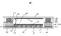
図1は、本発明の一実施形態が適用された液晶表示装置の断面図である。図示するように、液晶表示装置は、第1の基板10と、第2の基板20と、液晶層30と、シール部60とからなる。
FIG. 1 is a cross-sectional view of a liquid crystal display device to which an embodiment of the present invention is applied. As shown in the figure, the liquid crystal display device includes a
第1の基板10は、いわゆるカラーフィルタ基板である。第1の基板10は、第2の基板20に対向する面に、ブラックマトリックス層11と、R(赤)、G(緑)、B(青)の着色レジスト層12と、着色レジスト層12を平坦化するためのオーバコート層13と、配向膜14とを有している。
The
なお、図1の液晶表示装置は、IPS(In−Plane−Switching)方式であるため、第1の基板10に透明電極層が存在しない。しかし、本発明は、IPS方式以外の液晶表示装置にも適用可能であり、その場合は、第1の基板10のオーバコート層13と、配向膜14との間に、透明電極層が存在することになる。
1 is an IPS (In-Plane-Switching) system, the transparent electrode layer does not exist on the
第2の基板20は、いわゆるTFT基板であり、第1の基板に対向する面に、配向膜21を有している。
The
液晶層30は、第1の基板10と第2の基板20とに挟持され、配向膜14及び配向膜21により配向している。
The
シール部60は、第1の基板10と第2の基板20との間に挟まれた液晶30を密封するために設けられている。シール部60は、液晶表装置を上面からみたとき、液晶30の充填領域を囲うような、矩形状の閉曲線で表される(図2(C)、(D)の斜視図を参照
)。シール部60は、シール材台座層40と、シール材50とからなる。
The
シール材台座層40は、第1の基板10と第2の基板20とを貼り合わせるときに塗布されるシール材50の台座である。シール材台座層40は、シール材50の層の厚さ(シールギャップ)nを、液晶30の表示領域に相当する部分の厚さ(セルギャップ)mと同じか又はmより狭くするために設けられている。シール材台座層40の厚さL1は、第1の
基板10上に形成されたカラーフィルタ層の表示領域に相当する部分の厚さL2と同じか又はL2より厚くする。
The sealing
シール材台座層40の厚さL1は、例えば、1〜4μmの範囲であり、カラーフィルタ層の厚さL2比べて、0〜3μm程度、厚いのが好ましい。
The thickness L1 of the sealing
シール材台座層40の材質には特に制限はないが、カラーフィルタを形成する工程で同時に形成した場合、ブラックマトリックス11と同じ材料の層41、着色レジスト層12と同じ材料の層42、オーバコート層13と同じ材料の層43とが積層して形成される。
The material of the sealing
シール材50は、シール台座層40と第2の基板20とを接着する。シール材台座層40の存在により、シール材50の層の厚さ(シールギャップ)nは、液晶30の表示領域に
相当する部分の厚さ(セルギャップ)mと同じか又はmより狭い。
The sealing
セルギャップmは、通常、3〜5μmの範囲であるので、シールギャップnは、1〜5μmの範囲であるのが好ましい。シールギャップnが大きすぎると、シール材50への液晶30の入り込み現象が生じやすくなり、小さすぎると、接着信頼性が低下する。
Since the cell gap m is usually in the range of 3 to 5 μm, the seal gap n is preferably in the range of 1 to 5 μm. If the seal gap n is too large, the phenomenon of the
シール材50の材料は、液晶表示装置の基板の貼り合わせに一般的に用いられるものが使用できる。シール材50には、所望のシールギャップnを確保するために、スペーサ部材(ギャップ材)52が含まれている。スペーサ部材52は、絶縁体の微粒子で変形しないものが好ましい。例えば、径1μmのシリカビーズやシリカファイバである。
As the material of the sealing
次に、上記のように構成される液晶表示装置のパネルの製造方法について説明する。なお、本実施形態の製造方法は、2枚の基板の貼り合わせ工程に特徴がある。それ以外のパネル製造工程については、公知の方法を採用できるので、説明を省略する。 Next, the manufacturing method of the panel of the liquid crystal display device comprised as mentioned above is demonstrated. In addition, the manufacturing method of this embodiment has the characteristics in the bonding process of two board | substrates. Since the other panel manufacturing process can employ a known method, the description thereof is omitted.
本実施形態では、液晶の充填方法として、液晶滴下法を用いる。そして、その際のシール材の塗布に工夫をしている。 In this embodiment, a liquid crystal dropping method is used as a liquid crystal filling method. And it is devised in the application of the sealing material in that case.
図2は、第1の基板10と第2の基板20とを貼り合わせるまでの工程を説明するための図である。
FIG. 2 is a diagram for explaining a process until the
本実施形態の製造方法は、液晶滴下量のばらつきの影響を受け易い小型パネルの製造に好適である。例えば、パネルサイズ(対角寸法)は、0.8〜12インチのパネルである。基板サイズには制限が無く、その主面への小型パネルの多面付けが可能である。 The manufacturing method of this embodiment is suitable for manufacturing a small panel that is easily affected by variations in the amount of liquid crystal dripping. For example, the panel size (diagonal dimension) is a 0.8 to 12 inch panel. The substrate size is not limited, and multiple panels can be attached to the main surface.
なお、第1の基板には、対向する第2の基板との間隔を適切に保持するための高さ約4μmのギャップ材(スペーサ)が配置されているとする。 It is assumed that a gap material (spacer) having a height of about 4 μm is disposed on the first substrate in order to appropriately maintain a distance from the opposing second substrate.
第1の基板10に、シール台座層40を形成する(図2(A),(B)参照)。シール台座層40は、液晶30の充填領域を囲うように形成する。また、液晶が漏れないようにする必要があるので、閉曲線となるように形成する。線幅は約0.8mmである。なお、シール台座層40の上に塗布されるシール材50の線幅は、約0.65mmである。シール材50のパターニング精度が±0.1mmであるとすると、シール台座層40の線幅は、シール材50の線幅よりも0.1mm以上広くなるようにすると良い。
A
シール台座層40は、カラーフィルタ層の形成工程を利用して形成することができる。すなわち、フォトリソグラフィにより、ブラックマトリックス層11、RGBの着色レジスト層12、オーバコート層14を順に形成する際に、シール部60に相当する位置にも、これらに対応する層41、42、43を積層させる。これにより、表示領域のカラーフィルタ層より、3μm程度高いシール台座層40が形成できる。
The
例えば、セルギャップ3.0μmの液晶表示装置を作製する場合、カラーフィルタ層およびシール台座層40を構成する層の膜厚を次のようにすることができる。
着色レジスト層12(対応する層42)の膜厚=0.7μm
ブラックマトリクス層11(対応する層41)の膜厚=1.0μm
オーバーコート層13(対応する層43)の膜厚=1.1μm
かかる場合、シール台座層40の膜厚L1=4.1μmとなる。このとき、m+L2=3.0μm+2.1μm=5.1μmである。そこで、n=5.1μm−4.1μm+0.1μm=1.1μmとなるスペーサ部材(ギャップ材)52をシール材50へ添加してシールパターンを形成すればよい。
For example, when a liquid crystal display device having a cell gap of 3.0 μm is manufactured, the thicknesses of the layers constituting the color filter layer and the
Film thickness of the colored resist layer 12 (corresponding layer 42) = 0.7 μm
Film thickness of black matrix layer 11 (corresponding layer 41) = 1.0 μm
Film thickness of overcoat layer 13 (corresponding layer 43) = 1.1 μm
In such a case, the film thickness L1 of the
また、上記のような各層の厚さのままセルギャップ4.0μmの液晶表示装置を形成するには、n=2.1μmとなるスペーサ部材(ギャップ材)52をシール材へ添加してシールパターンを形成すればよい。 In addition, in order to form a liquid crystal display device having a cell gap of 4.0 μm with the thickness of each layer as described above, a spacer member (gap material) 52 with n = 2.1 μm is added to the sealing material to form a sealing pattern. May be formed.
一方、2.0μmの液晶表示装置を作製する場合、シール台座層40に形成する着色レジスト層12の内の一色分の層42を除き、L1=3.4μmとする。m+L2=2.0μm+2.1μm=4.1μmであるので、n=0.8μmとなるスペーサ部材(ギャップ材)52をシール材50へ添加してシールパターンを形成すればよい。
On the other hand, when a 2.0 μm liquid crystal display device is manufactured, L1 = 3.4 μm, except for the
なお、シール台座層40は、カラーフィルタ層の形成後に、単独で樹脂前駆体を硬化させて形成することもできる。例えば、シール部60に相当する位置に、ホトリソグラフィ、ディスペンサやスクリーン印刷法により、シール台座層40の材料でパターンを形成する。かかる場合のシール台座層40の材料としては、アクリレート樹脂などを用いることができる。樹脂前駆体で形成されたシール台座層40は、シール材50のパターニング以前に硬化するものが好ましく、常温では流動しないものがよい。
The
こうして、シール台座層40を形成すると、次に、配向膜14を形成する。その後、ディスペンサやスクリーン印刷法により、シール台座層40上に、シール材50のパターンを形成する(図2(C)参照)。
After the
なお、配向膜14は、0.1μm程度である。そこで、配向膜14を形成する工程を利用して、シール台座層40に、配向膜14に対応する層をさらに積層させてもよい。そして、配向膜14の層を積層したシール台座層40上に、シール材50のパターンを形成するようにしてもよい。
The alignment film 14 is about 0.1 μm. Therefore, a layer corresponding to the alignment film 14 may be further laminated on the
このとき、第1の基板10に、外縁に沿った外周シール枠80も設けてもよい。外周シール枠80を設けるのは、2枚の基板を貼り合わせたときに、外周シール枠80と内側のシール材50のパターンとの間の領域を真空に封止するためである。この領域を真空にすれば、大気圧に戻したときに、大気圧を利用して、確実に圧着を行うことができる。外周シール枠80は、面取り工程において、切り捨てられる部分であり、液晶を封止するシール材80のパターンとその役目が実質的に異なる。なお、このような機能を持った外周シール枠80は、複数設けてもよい。
At this time, the outer
シール材50の材料は、液晶表示装置の基板の貼り合わせに通常用いられるものでよい。例えば、アクリレート樹脂、変性エポキシ樹脂などの紫外線硬化性樹脂である。シール材50には、2枚の基板を貼り合わせたときのシール材50の層を所望の厚さに確保するために、スペーサ部材(ギャップ材)が配合してある。スペーサ部材は、絶縁体の微粒子が好ましい。例えば、径1μm程度のビーズやシリコンファイバが0.5〜5%配合されている。
The material of the sealing
なお、シール材50のパターンは、第2の基板20のシール部60に対応する位置に形成してもよい。
Note that the pattern of the sealing
次に、真空中で、表示領域に、液晶30を1,2滴、滴下し、2枚の基板を貼り合わせて封着する(図2(D)参照)。そして、大気圧に戻した後、紫外線照射を行い、さらに加熱炉で120℃程度で、約1時間加熱してシール材50を硬化させる。
Next, in a vacuum, one or two drops of the
以上、2枚の基板を貼り合わせ、液晶を充填する工程について説明した。その後は、公知の製造プロセス(洗浄、面取り工程、偏光板張付け工程など)により、液晶表示装置が完成する。 The process of bonding two substrates and filling the liquid crystal has been described above. Thereafter, the liquid crystal display device is completed by a known manufacturing process (cleaning, chamfering step, polarizing plate pasting step, etc.).
以上、本発明の一実施形態が適用された液晶表示装置及びその製造方法について説明した。 The liquid crystal display device to which the embodiment of the present invention is applied and the manufacturing method thereof have been described above.
上記実施形態によれば、過剰量の液晶30が滴下された場合における、液晶30のシール部60への入り込みや漏れを抑制できる。すなわち、図3で示されるような、液晶30がシール材50に入り込んでしまう現象を抑制できる。図中、符号51は、シール材50に入り込んでしまった液晶30を示す。上記実施形態によれば、このような入り込み51の度合いkを抑制できる。すなわち、従来の方法にくらべ、滴下量がより”おおざっぱ”であっても、仕様として許容されるセルギャップを備えたパネルを製造することができる。
According to the embodiment, it is possible to prevent the
本発明は、上記実施形態に制限されることない。上記実施形態は、様々な変形が可能である。 The present invention is not limited to the above embodiment. The above embodiment can be variously modified.
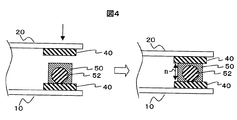
例えば、シール材台座層40は、第1の基板10と第2の基板20の少なくとも一方に設けられていればよい。すなわち、第2の基板20に設けるようにしてもよい。
For example, the sealing
また、図4(液晶表示装置の端部の断面図)に示すように、二つの基板の両方にシール材台座層40を設けるようにしてもよい。このようにしてもシールギャップnを狭くすることができる。
Further, as shown in FIG. 4 (a cross-sectional view of the end portion of the liquid crystal display device), a sealing
また、図5(液晶表示装置の端部の断面図)に示すように、シール台座層40に、ギャップ材52が嵌まり込むことが可能な溝40hを設けてもよい。このような溝は、両側に土手となる樹脂層をフォトリソグラフィなどで形成すれば、形成できる。こうすれば、ギャップ材52を確実にシール台座層40の所定の位置に留め置くことができ、所望のシールギャップnを容易に達成することができる。ギャップ材52は、溝40hに完全に埋もれることがないよういな大きさである。具体的には、ギャップ材52の高さ(ビーズの場合、直径)/溝40hの深さは1.1以上であるのが好ましい。1.1よりも小さい場合、ギャップ材52とシール台座層40の高さが近接してしまい、シール台座層40と対向基板(第2の基板20)とが接触することがある。その場合、シール台座層40の上面は平面であるため、シール材50がシール台座層40と対向基板間に残存する。このとき、シール材50の残存量が部分的に異なるとセルギャップのばらつきの原因となる。
Further, as shown in FIG. 5 (a cross-sectional view of the end portion of the liquid crystal display device), a
また、図6(液晶表示装置の端部の断面図)に示すように、シール台座層40の形状を、断面が円弧(いいかえれば、かまぼこ型)で、盛り上がるように形成してもよい。このように、天頂40tが曲面になるようにすれば、対向する基板と、面ではなく、線により、接触するようになるので、密着性が向上する。すなわち、天頂が平面の場合、シール台座層40と対向基板(第2の基板20)との間に存在するシール材50の残存量のばらつきを低減でき、ギャップのばらつきを抑えることができる。
Further, as shown in FIG. 6 (cross-sectional view of the end portion of the liquid crystal display device), the shape of the
<実施例>
以下に、本発明の実施例を説明するが、本発明はこれに限定されるものではない。
<Example>
Examples of the present invention will be described below, but the present invention is not limited thereto.
本実施例では、図1に示した液晶表示装置を、図2に示した製造工程により作製した。具体的には、42×31.5の2インチサイズの小型液晶ディスプレイパネルを作製した。なお、ギャップ材として、直径4μmのポリスチレンビーズを使用した。 In this example, the liquid crystal display device shown in FIG. 1 was manufactured by the manufacturing process shown in FIG. Specifically, a 42 × 31.5 2-inch small liquid crystal display panel was produced. As the gap material, polystyrene beads having a diameter of 4 μm were used.
第1の基板(カラーフィルタ基板)10を作製する際、シール部60に相当する位置に、ブラックマトリックス層、R,G、Bの着色レジスト層を重ね、更にその上にオーバコート層を成膜した。そして、表示領域の層の厚さL2よりも厚さL1が3μm厚いシール材台座層40を作製した。このときのブラックマトリックス11は、約1μmの樹脂である。
When the first substrate (color filter substrate) 10 is manufactured, a black matrix layer, R, G, and B colored resist layers are overlaid on the position corresponding to the
次に、第1の基板10の表示領域に配向膜14を成膜した後、ディスペンサによりシール材台座層40上にシール材50を塗布した。シール材50は、紫外線硬化性樹脂であり、径1μmのシリカファイバ52を0.5%配合してある。
Next, after the alignment film 14 was formed in the display area of the
次に、液晶30を2滴、表示領域に滴下し、第2の基板(TFT基板)10を位置あわせして、真空チャンバの中で貼り合わせた。
Next, two drops of the
チャンバ内を大気圧に戻した後、貼り合わせた基板を取り出し、紫外線照射を行い、さらに加熱炉で120℃で、1時間加熱してシール材50を硬化させた。その後、基板を切断して、液晶表示装置のパネルが完成した。
After returning the inside of the chamber to atmospheric pressure, the bonded substrates were taken out, irradiated with ultraviolet rays, and further heated at 120 ° C. for 1 hour in a heating furnace to cure the sealing
完成したパネルにおいては、液晶漏れは発生せず、また図3に示したような内部の液晶30がシール材50に入り込む現象も見られなかった。
In the completed panel, liquid crystal leakage did not occur, and the phenomenon that the
以上、本願発明の実施形態及び実施例について説明した。 Heretofore, the embodiments and examples of the present invention have been described.
最後に、本願発明に含まれるシール台座層40の形状及び配置についてまとめる。
Finally, the shape and arrangement of the
図7〜図14は、シール部の断面図である。それぞれ、2つの基板10、20の貼り合わせ前後の様子(「左の図」は、貼り合わせ前である。「右の図」は、貼り合わせ後である。)を示している。それぞれの図において、シール部の左側は、液晶30が充填され表示領域となるパネルの内部(inside)である。
7 to 14 are sectional views of the seal portion. Each shows a state before and after the bonding of the two
図7(A)に示すように、第1の基板(カラーフィルタ基板)10に、シール台座層40を形成することができる。これは、上記実施形態で説明した態様である。かかる場合、シール台座層40は、カラーフィルタ(着色レジスト層、ブラックマトリックス層)の形成に使用する材料により、カラーフィルタを形成する層の形成とともに、形成することができる。
As shown in FIG. 7A, the
また、図7(B)に示すように、第2の基板(TFT基板)20に、シール台座層40を形成することもできる。かかる場合、シール台座層40は、TFT(配線膜、絶縁膜、保護膜等)の形成に使用する材料により、TFTを形成する層の形成とともに、形成することができる。
Further, as shown in FIG. 7B, a
また、図7(C)に示すように、第1の基板10及び第2の基板20の両方に、シール台座層40a、40bをそれぞれ形成してもよい。かかる場合、シール台座層40a、40bのそれぞれを厚膜にする必要がなく、製造工程が簡略化できる。
Further, as shown in FIG. 7C, seal pedestal layers 40a and 40b may be formed on both the
また、図8(A)に示すように、シール台座層40は、内側と外側に2つの土手40mと40nを備え、その間に、溝40hを形成していてもよい。土手40m及び40nは、表示領域を囲うような閉ループを描いている。溝40hに、ギャップ材52を含むシール材50が塗布される。これは、上述の図5に対応する。かかる場合、シールギャップnを極めて狭めることができ、液晶30に接触するシール材50の面積を少なくでき、シール材50の汚染を抑制できる。
Further, as shown in FIG. 8A, the
また、図8(B)に示すように、シール台座層40は、内側の土手40mのみを備えていてもよい。かかる場合でも、シールギャップnを極めて狭めることができ、液晶30に接触するシール材50の面積を少なくでき、シール材50の汚染を抑制できる。
Further, as shown in FIG. 8B, the
また、必要に応じて、図8(C)に示すように、シール台座層40は、外側の土手40nのみを備えていてもよい。
Moreover, as shown in FIG.8 (C), the
また、図9(A)に示すように、第1の基板10に、土手40m及び土手40nを形成し、その間に溝40hを形成してもよい。そして、第2の基板20には、土手40m、溝40h、及び土手40nを覆うように、一連のシール台座層40aを形成する。土手40m及び40nは、表示領域を囲うような閉ループを描いている。溝40hに、ギャップ材52を含むシール材50が塗布される。こうすれば、それぞれの層を厚膜とする必要がない。また、シールギャップnを極めて狭めることができ、液晶30に接触するシール材50の面積を少なくでき、シール材50の汚染を抑制できる。
Further, as shown in FIG. 9A, a
また、図9(B)に示すように、上記図9(A)における土手40nを設けない態様も、実施可能である。かかる場合でも、シールギャップnを極めて狭めることができ、液晶30に接触するシール材50の面積を少なくでき、シール材50の汚染を抑制できる。
Further, as shown in FIG. 9B, a mode in which the
また、必要に応じて、図9(C)に示すように、上記図9(A)における土手40mを設けない態様も、実施可能である。
Moreover, as shown in FIG.9 (C), the aspect which does not provide the
また、図10(A)及び図10(B)に示すように、上記図8Aにおける土手40m及び土手40nの幅を非対称にしてもよい。また、図10(C)及び図10(D)に示すように、図9(A)における土手40m及び40nの幅を非対称にしてもよい。例えば、内側の土手40mの幅を外側の土手40nの幅より太くする。または、内側の土手40mの幅を外側の土手40nの幅より狭くする。いずれにするかは、設計思想に基づいて適宜選択すればよい。
Further, as shown in FIGS. 10A and 10B, the widths of the
また、土手40m、40nの幅は一定でなくてもよい。土手40m、40nが形成されている基板(第1の基板10又は第2の基板20)からの距離に応じてその幅が変化するように形成してもよい。図11〜図14は、かかる場合の例を示す。
Further, the widths of the
図11(A)、図11(B)、図11(C)、及び図11(D)は、それぞれ上記の図8(A)、図8(B)、図8(C)、及び図9(A)に対応する。土手40m、40nの、シール材50を塗布する位置から遠い面(土手40mの場合、表示領域側の面。土手40nの場合、表示領域側の逆側の面。)は、基板におよそ垂直である。一方、シール材50を塗布する位置に近い面(土手40mの場合、表示領域側の逆側の面。土手40nの場合、表示領域側の面。)は、階段状または斜面となっている。すなわち、土手40m、40nは、その幅が第1の基板10から遠くなるほど狭くなるように形成されている。図11(A)では、溝40hは、深い部分ほど、その幅が狭くなる。
11 (A), FIG. 11 (B), FIG. 11 (C), and FIG. 11 (D) are the above-mentioned FIG. 8 (A), FIG. 8 (B), FIG. 8 (C), and FIG. Corresponds to (A). The surfaces of the
図12(A)、図12(B)、図12(C)、及び図12(D)は、それぞれ上記の図8(A)、図8(B)、図8(C)、及び図9(A)に対応する。土手40m、40nの、シール材50を塗布する位置から近い面(土手40mの場合、表示領域側の逆側の面。土手40nの場合、表示領域側の面。)は、基板におよそ垂直である。一方、シール材50を塗布する位置に遠い面(土手40mの場合、表示領域側の面。土手40nの場合、表示領域側の逆側の面。)は、階段状または斜面となっている。
FIGS. 12A, 12B, 12C, and 12D are respectively the same as FIGS. 8A, 8B, 8C, and 9 described above. Corresponds to (A). The surfaces of the
図13(A)、図13(B)、及び図13(C)は、それぞれ上記の図8(A)、図8(B)、及び図8(C)に対応する。土手40m、40nは、シール材50を塗布する位置から近い面(土手40mの場合、表示領域側の逆側の面。土手40nの場合、表示領域側の面。)、及びシール材50を塗布する位置に遠い面(土手40mの場合、表示領域側の面。土手40nの場合、表示領域側の逆側の面。)の両方の面において、階段状または斜面となっている。
FIGS. 13A, 13B, and 13C correspond to FIGS. 8A, 8B, and 8C, respectively. The
図14(A)、図14(B)、及び図14(C)は、それぞれ上記の図9(A)、図9(B)、及び図9(C)に対応する。土手40m、40nは、シール材50を塗布する位置から近い面(土手40mの場合、表示領域側の逆側の面。土手40nの場合、表示領域側の面。)、及びシール材50を塗布する位置に遠い面(土手40mの場合、表示領域側の面。土手40nの場合、表示領域側の逆側の面。)の両方の面において、階段状または斜面となっている。
14A, 14B, and 14C correspond to the above-described FIGS. 9A, 9B, and 9C, respectively. The
10・・・第1の基板(カラーフィルタ基板)
11・・・ブラックマトリックス、12・・・着色レジスト、13・・・オーバコート層
、
14・・・配向膜
20・・・第2の基板(TFT基板)、21・・・配向膜、
30・・・液晶
40・・・シール材台座層
50・・・シール材
52・・・ギャップ材
10: First substrate (color filter substrate)
11 ... Black matrix, 12 ... Color resist, 13 ... Overcoat layer,
14 ...
30 ...
Claims (8)
前記第1の基板と前記第2の基板とは、前記液晶の充填領域を囲うように設けられたシール材により接着されており、
前記第1の基板は、その基板上にカラーフィルタ層を有するカラーフィルタ基板であり、
前記第1の基板は、その上に前記シール材を備える台座層を有し、
前記シール材には、ギャップ材が含まれており、
前記台座層はその上に、溝と、当該溝よりも表示領域側に設けられた内側土手と、を有するとともに、前記シール材は、前記溝の内部及び前記内側土手の上に設けられており、前記ギャップ材は、前記溝の内部に設けられており、
前記台座層の厚さは、表示領域に対応する前記カラーフィルタ層の厚さよりも厚く、かつ前記液晶の層の厚さよりも厚く、
前記シール材の層の厚さは、表示領域に相当する部分の液晶の層の厚さ以下であり、
前記カラーフィルタ層より厚い台座層と前記液晶の層よりも薄いシール材とが、前記表示領域の全周にわたって形成されている
ことを特徴とする液晶表示装置。 A liquid crystal display device in which a liquid crystal is sandwiched between a first substrate and a second substrate,
The first substrate and the second substrate are bonded by a sealing material provided so as to surround the liquid crystal filling region,
The first substrate is a color filter substrate having a color filter layer on the substrate;
The first substrate has a pedestal layer provided with the sealing material thereon,
The sealing material includes a gap material,
The pedestal layer thereon, a groove, an inner bank provided in Table display region side than the groove, which has a, the sealing material is provided on the inside and the inner bank of the groove The gap material is provided inside the groove,
The thickness of the pedestal layer is thicker than the thickness of the color filter layer corresponding to the display area and thicker than the thickness of the liquid crystal layer,
The thickness of the sealing material layer is equal to or less than the thickness of the liquid crystal layer corresponding to the display region,
A liquid crystal display device, wherein a pedestal layer thicker than the color filter layer and a sealing material thinner than the liquid crystal layer are formed over the entire periphery of the display region.
前記台座層は、
前記第1の基板のカラーフィルタ層を形成する層と同様の層で形成されている
ことを特徴とする液晶表示装置。 The liquid crystal display device according to claim 1,
The pedestal layer is
A liquid crystal display device comprising: a layer similar to the layer forming the color filter layer of the first substrate.
前記台座層は、
前記第1の基板のカラーフィルタ層を形成する層とは別の層で形成されている
ことを特徴とする液晶表示装置。 The liquid crystal display device according to claim 1,
The pedestal layer is
A liquid crystal display device comprising: a layer different from a layer forming the color filter layer of the first substrate.
前記溝の外側の前記台座層上に、外側土手を有し、
前記シール材は、前記外側土手上にも設けられている
ことを特徴とする液晶表示装置。 The liquid crystal display device according to claim 1 ,
On the pedestal layer outside the groove, has an outer bank,
The liquid crystal display device, wherein the sealing material is also provided on the outer bank.
前記第1の基板上に形成され、溝と、それより内側の内側土手とを有する台座層上に前記液晶の充填領域を囲むように、ギャップ材を含むシール材を塗布するステップと、
前記台座層と前記シール材の内側に液晶を充填するステップと、
前記液晶の充填後に、前記第1の基板と前記第2の基板とを貼り合わせるステップとを有し、
前記シール材は、
前記第1の基板と前記第2の基板とを貼り合わせたときには、前記溝内と前記内側土手上に設けられるとともに、その層の厚さが、前記カラーフィルタ層が設けられた表示領域に相当する部分の液晶の層の厚さ以下になるように形成され、
前記ギャップ材は、前記溝の内部に設けられ、
前記台座層の厚さは、表示領域に対応する前記カラーフィルタ層の厚さよりも厚く、かつ前記液晶の層の厚さよりも厚く、
前記カラーフィルタ層より厚い台座層と前記液晶の層よりも薄いシール材とが、前記表示領域の全周にわたって形成されている
ことを特徴とする液晶表示装置の製造方法。 A color comprising a first substrate and a second substrate, wherein the first substrate and the second substrate sandwich a liquid crystal, and the first substrate has a color filter layer on the substrate. A method of manufacturing a liquid crystal display device which is a filter substrate,
Applying a sealing material including a gap material on the pedestal layer formed on the first substrate and having a groove and an inner bank on the inner side thereof, so as to surround the liquid crystal filling region;
Filling liquid crystal inside the pedestal layer and the sealing material;
Bonding the first substrate and the second substrate after filling with the liquid crystal,
The sealing material is
When the first substrate and the second substrate are bonded together, the first substrate and the second substrate are provided in the groove and on the inner bank, and the thickness of the layer corresponds to the display region provided with the color filter layer. Formed to be less than the thickness of the liquid crystal layer
The gap material is provided inside the groove,
The thickness of the pedestal layer is thicker than the thickness of the color filter layer corresponding to the display area and thicker than the thickness of the liquid crystal layer,
A manufacturing method of a liquid crystal display device, wherein a pedestal layer thicker than the color filter layer and a sealing material thinner than the liquid crystal layer are formed over the entire periphery of the display region.
前記台座層は、
前記第1の基板のカラーフィルタ層を形成する層と同様の層で形成される
ことを特徴とする液晶表示装置の製造方法。 It is a manufacturing method of the liquid crystal display device according to claim 5 ,
The pedestal layer is
A method of manufacturing a liquid crystal display device, comprising: forming a layer similar to the layer forming the color filter layer of the first substrate.
前記台座層は、
前記第1の基板のカラーフィルタ層を形成する層とは別の層で形成される
ことを特徴とする液晶表示装置の製造方法。 It is a manufacturing method of the liquid crystal display device according to claim 5 ,
The pedestal layer is
A method for manufacturing a liquid crystal display device, comprising: a layer different from a layer forming a color filter layer of the first substrate.
前記溝の外側の前記台座層上に、外側土手を有し、
前記シール材は、前記外側土手上にも設けられている
ことを特徴とする液晶表示装置の製造方法。 It is a manufacturing method of the liquid crystal display device according to claim 5 ,
On the pedestal layer outside the groove, has an outer bank,
The method for manufacturing a liquid crystal display device, wherein the sealing material is also provided on the outer bank.
Priority Applications (1)
| Application Number | Priority Date | Filing Date | Title |
|---|---|---|---|
| JP2007231345A JP5317445B2 (en) | 2006-09-07 | 2007-09-06 | Liquid crystal display device and manufacturing method thereof |
Applications Claiming Priority (3)
| Application Number | Priority Date | Filing Date | Title |
|---|---|---|---|
| JP2006242602 | 2006-09-07 | ||
| JP2006242602 | 2006-09-07 | ||
| JP2007231345A JP5317445B2 (en) | 2006-09-07 | 2007-09-06 | Liquid crystal display device and manufacturing method thereof |
Publications (3)
| Publication Number | Publication Date |
|---|---|
| JP2008090294A JP2008090294A (en) | 2008-04-17 |
| JP2008090294A5 JP2008090294A5 (en) | 2010-06-03 |
| JP5317445B2 true JP5317445B2 (en) | 2013-10-16 |
Family
ID=39374445
Family Applications (1)
| Application Number | Title | Priority Date | Filing Date |
|---|---|---|---|
| JP2007231345A Active JP5317445B2 (en) | 2006-09-07 | 2007-09-06 | Liquid crystal display device and manufacturing method thereof |
Country Status (1)
| Country | Link |
|---|---|
| JP (1) | JP5317445B2 (en) |
Families Citing this family (4)
| Publication number | Priority date | Publication date | Assignee | Title |
|---|---|---|---|---|
| JP5261300B2 (en) * | 2009-07-08 | 2013-08-14 | 株式会社ジャパンディスプレイ | Liquid crystal display |
| JP2012073356A (en) * | 2010-09-28 | 2012-04-12 | Mitsubishi Electric Corp | Liquid crystal display device |
| JP5942555B2 (en) * | 2012-04-11 | 2016-06-29 | 三菱電機株式会社 | Manufacturing method of liquid crystal display device |
| JP5492326B2 (en) * | 2013-04-26 | 2014-05-14 | 株式会社ジャパンディスプレイ | Manufacturing method of liquid crystal display device |
Family Cites Families (5)
| Publication number | Priority date | Publication date | Assignee | Title |
|---|---|---|---|---|
| JPH07230095A (en) * | 1994-02-17 | 1995-08-29 | Matsushita Electric Ind Co Ltd | Liquid crystal display panel |
| JPH07311378A (en) * | 1994-05-18 | 1995-11-28 | Toppan Printing Co Ltd | Liquid crystal display device |
| JP2000056317A (en) * | 1998-08-11 | 2000-02-25 | Toshiba Corp | Liquid crystal display device and production of the same |
| JP3937304B2 (en) * | 2002-01-10 | 2007-06-27 | 鹿児島日本電気株式会社 | Manufacturing method of liquid crystal display panel |
| KR20060028536A (en) * | 2004-09-24 | 2006-03-30 | 삼성전자주식회사 | Color filter array panel and liquid crystal display include the same |
-
2007
- 2007-09-06 JP JP2007231345A patent/JP5317445B2/en active Active
Also Published As
| Publication number | Publication date |
|---|---|
| JP2008090294A (en) | 2008-04-17 |
Similar Documents
| Publication | Publication Date | Title |
|---|---|---|
| JP5934797B2 (en) | Display panel | |
| US8120743B2 (en) | Liquid crystal display device and production method thereof | |
| US10509255B2 (en) | Liquid crystal panel comprising a composite polarizing layer having a first polarizing layer and a second polarizing layer that covers a groove formed in a black matrix in a non-display area and liquid crystal display device | |
| JP4850612B2 (en) | Liquid crystal display | |
| WO2016061850A1 (en) | Manufacturing method for curved liquid crystal panel | |
| KR20020093984A (en) | A liquid crystal display device | |
| WO2018166133A1 (en) | Display substrate and display panel | |
| JP2001209060A (en) | Method of producing liquid crystal display panel | |
| US7929103B2 (en) | Display and method of manufacturing display | |
| WO2020087658A1 (en) | Display panel and display device | |
| JP2011053308A (en) | Display device and method of manufacturing the same | |
| WO2021007951A1 (en) | Substrate and liquid crystal display panel | |
| JP2016164617A (en) | Method for manufacturing liquid crystal cell, method for manufacturing dimming material, and method for manufacturing glass laminate | |
| JP4335632B2 (en) | Manufacturing method of liquid crystal display device | |
| JP5317445B2 (en) | Liquid crystal display device and manufacturing method thereof | |
| WO2018148991A1 (en) | Liquid crystal display panel | |
| WO2013183216A1 (en) | Display panel and method for manufacturing same | |
| WO2017063394A1 (en) | Liquid crystal cell, method for preparing liquid crystal cell, and display panel | |
| JP2016161862A (en) | Method for manufacturing liquid crystal cell, method for manufacturing dimming material, and method for manufacturing glass laminate | |
| JP4851651B2 (en) | Liquid crystal display element | |
| JPH05323337A (en) | Liquid crystal display panel and its production | |
| JP2010224491A (en) | Liquid crystal display panel | |
| JP4320339B2 (en) | Manufacturing method of liquid crystal panel | |
| JP2001318387A (en) | Liquid crystal display panel and its manufacturing method | |
| JP2009128799A (en) | Liquid crystal display and method for manufacturing the same |
Legal Events
| Date | Code | Title | Description |
|---|---|---|---|
| A521 | Request for written amendment filed |
Free format text: JAPANESE INTERMEDIATE CODE: A523 Effective date: 20100303 |
|
| A621 | Written request for application examination |
Free format text: JAPANESE INTERMEDIATE CODE: A621 Effective date: 20100303 |
|
| A521 | Request for written amendment filed |
Free format text: JAPANESE INTERMEDIATE CODE: A523 Effective date: 20100419 |
|
| A711 | Notification of change in applicant |
Free format text: JAPANESE INTERMEDIATE CODE: A712 Effective date: 20110228 |
|
| RD03 | Notification of appointment of power of attorney |
Free format text: JAPANESE INTERMEDIATE CODE: A7423 Effective date: 20110228 |
|
| A977 | Report on retrieval |
Free format text: JAPANESE INTERMEDIATE CODE: A971007 Effective date: 20111228 |
|
| A131 | Notification of reasons for refusal |
Free format text: JAPANESE INTERMEDIATE CODE: A131 Effective date: 20120131 |
|
| A521 | Request for written amendment filed |
Free format text: JAPANESE INTERMEDIATE CODE: A523 Effective date: 20120330 |
|
| RD02 | Notification of acceptance of power of attorney |
Free format text: JAPANESE INTERMEDIATE CODE: A7422 Effective date: 20120330 |
|
| RD04 | Notification of resignation of power of attorney |
Free format text: JAPANESE INTERMEDIATE CODE: A7424 Effective date: 20120409 |
|
| A131 | Notification of reasons for refusal |
Free format text: JAPANESE INTERMEDIATE CODE: A131 Effective date: 20121023 |
|
| A521 | Request for written amendment filed |
Free format text: JAPANESE INTERMEDIATE CODE: A523 Effective date: 20121218 |
|
| TRDD | Decision of grant or rejection written | ||
| A01 | Written decision to grant a patent or to grant a registration (utility model) |
Free format text: JAPANESE INTERMEDIATE CODE: A01 Effective date: 20130702 |
|
| A61 | First payment of annual fees (during grant procedure) |
Free format text: JAPANESE INTERMEDIATE CODE: A61 Effective date: 20130709 |
|
| R150 | Certificate of patent or registration of utility model |
Ref document number: 5317445 Country of ref document: JP Free format text: JAPANESE INTERMEDIATE CODE: R150 Free format text: JAPANESE INTERMEDIATE CODE: R150 |
|
| R250 | Receipt of annual fees |
Free format text: JAPANESE INTERMEDIATE CODE: R250 |
|
| R250 | Receipt of annual fees |
Free format text: JAPANESE INTERMEDIATE CODE: R250 |
|
| R250 | Receipt of annual fees |
Free format text: JAPANESE INTERMEDIATE CODE: R250 |
|
| R250 | Receipt of annual fees |
Free format text: JAPANESE INTERMEDIATE CODE: R250 |
|
| R250 | Receipt of annual fees |
Free format text: JAPANESE INTERMEDIATE CODE: R250 |
|
| R250 | Receipt of annual fees |
Free format text: JAPANESE INTERMEDIATE CODE: R250 |
|
| R250 | Receipt of annual fees |
Free format text: JAPANESE INTERMEDIATE CODE: R250 |
|
| R250 | Receipt of annual fees |
Free format text: JAPANESE INTERMEDIATE CODE: R250 |
|
| S111 | Request for change of ownership or part of ownership |
Free format text: JAPANESE INTERMEDIATE CODE: R313117 |
|
| R350 | Written notification of registration of transfer |
Free format text: JAPANESE INTERMEDIATE CODE: R350 |