JP5301269B2 - Masks and methods for electrokinetic deposition and patterning processes on substrates - Google Patents
Masks and methods for electrokinetic deposition and patterning processes on substrates Download PDFInfo
- Publication number
- JP5301269B2 JP5301269B2 JP2008512507A JP2008512507A JP5301269B2 JP 5301269 B2 JP5301269 B2 JP 5301269B2 JP 2008512507 A JP2008512507 A JP 2008512507A JP 2008512507 A JP2008512507 A JP 2008512507A JP 5301269 B2 JP5301269 B2 JP 5301269B2
- Authority
- JP
- Japan
- Prior art keywords
- substrate
- mask
- particles
- charged particles
- conductive layer
- Prior art date
- Legal status (The legal status is an assumption and is not a legal conclusion. Google has not performed a legal analysis and makes no representation as to the accuracy of the status listed.)
- Expired - Fee Related
Links
Images


Classifications
-
- H—ELECTRICITY
- H01—ELECTRIC ELEMENTS
- H01L—SEMICONDUCTOR DEVICES NOT COVERED BY CLASS H10
- H01L21/00—Processes or apparatus adapted for the manufacture or treatment of semiconductor or solid state devices or of parts thereof
- H01L21/02—Manufacture or treatment of semiconductor devices or of parts thereof
- H01L21/027—Making masks on semiconductor bodies for further photolithographic processing not provided for in group H01L21/18 or H01L21/34
- H01L21/0271—Making masks on semiconductor bodies for further photolithographic processing not provided for in group H01L21/18 or H01L21/34 comprising organic layers
- H01L21/0273—Making masks on semiconductor bodies for further photolithographic processing not provided for in group H01L21/18 or H01L21/34 comprising organic layers characterised by the treatment of photoresist layers
- H01L21/0274—Photolithographic processes
-
- B—PERFORMING OPERATIONS; TRANSPORTING
- B23—MACHINE TOOLS; METAL-WORKING NOT OTHERWISE PROVIDED FOR
- B23K—SOLDERING OR UNSOLDERING; WELDING; CLADDING OR PLATING BY SOLDERING OR WELDING; CUTTING BY APPLYING HEAT LOCALLY, e.g. FLAME CUTTING; WORKING BY LASER BEAM
- B23K3/00—Tools, devices, or special appurtenances for soldering, e.g. brazing, or unsoldering, not specially adapted for particular methods
- B23K3/06—Solder feeding devices; Solder melting pans
- B23K3/0607—Solder feeding devices
- B23K3/0623—Solder feeding devices for shaped solder piece feeding, e.g. preforms, bumps, balls, pellets, droplets
-
- C—CHEMISTRY; METALLURGY
- C25—ELECTROLYTIC OR ELECTROPHORETIC PROCESSES; APPARATUS THEREFOR
- C25D—PROCESSES FOR THE ELECTROLYTIC OR ELECTROPHORETIC PRODUCTION OF COATINGS; ELECTROFORMING; APPARATUS THEREFOR
- C25D13/00—Electrophoretic coating characterised by the process
-
- C—CHEMISTRY; METALLURGY
- C25—ELECTROLYTIC OR ELECTROPHORETIC PROCESSES; APPARATUS THEREFOR
- C25D—PROCESSES FOR THE ELECTROLYTIC OR ELECTROPHORETIC PRODUCTION OF COATINGS; ELECTROFORMING; APPARATUS THEREFOR
- C25D13/00—Electrophoretic coating characterised by the process
- C25D13/22—Servicing or operating apparatus or multistep processes
-
- C—CHEMISTRY; METALLURGY
- C25—ELECTROLYTIC OR ELECTROPHORETIC PROCESSES; APPARATUS THEREFOR
- C25D—PROCESSES FOR THE ELECTROLYTIC OR ELECTROPHORETIC PRODUCTION OF COATINGS; ELECTROFORMING; APPARATUS THEREFOR
- C25D15/00—Electrolytic or electrophoretic production of coatings containing embedded materials, e.g. particles, whiskers, wires
-
- C—CHEMISTRY; METALLURGY
- C25—ELECTROLYTIC OR ELECTROPHORETIC PROCESSES; APPARATUS THEREFOR
- C25D—PROCESSES FOR THE ELECTROLYTIC OR ELECTROPHORETIC PRODUCTION OF COATINGS; ELECTROFORMING; APPARATUS THEREFOR
- C25D5/00—Electroplating characterised by the process; Pretreatment or after-treatment of workpieces
- C25D5/02—Electroplating of selected surface areas
- C25D5/022—Electroplating of selected surface areas using masking means
-
- H—ELECTRICITY
- H01—ELECTRIC ELEMENTS
- H01L—SEMICONDUCTOR DEVICES NOT COVERED BY CLASS H10
- H01L21/00—Processes or apparatus adapted for the manufacture or treatment of semiconductor or solid state devices or of parts thereof
- H01L21/02—Manufacture or treatment of semiconductor devices or of parts thereof
- H01L21/04—Manufacture or treatment of semiconductor devices or of parts thereof the devices having at least one potential-jump barrier or surface barrier, e.g. PN junction, depletion layer or carrier concentration layer
- H01L21/18—Manufacture or treatment of semiconductor devices or of parts thereof the devices having at least one potential-jump barrier or surface barrier, e.g. PN junction, depletion layer or carrier concentration layer the devices having semiconductor bodies comprising elements of Group IV of the Periodic System or AIIIBV compounds with or without impurities, e.g. doping materials
- H01L21/28—Manufacture of electrodes on semiconductor bodies using processes or apparatus not provided for in groups H01L21/20 - H01L21/268
- H01L21/283—Deposition of conductive or insulating materials for electrodes conducting electric current
- H01L21/288—Deposition of conductive or insulating materials for electrodes conducting electric current from a liquid, e.g. electrolytic deposition
- H01L21/2885—Deposition of conductive or insulating materials for electrodes conducting electric current from a liquid, e.g. electrolytic deposition using an external electrical current, i.e. electro-deposition
-
- H—ELECTRICITY
- H01—ELECTRIC ELEMENTS
- H01L—SEMICONDUCTOR DEVICES NOT COVERED BY CLASS H10
- H01L24/00—Arrangements for connecting or disconnecting semiconductor or solid-state bodies; Methods or apparatus related thereto
- H01L24/01—Means for bonding being attached to, or being formed on, the surface to be connected, e.g. chip-to-package, die-attach, "first-level" interconnects; Manufacturing methods related thereto
- H01L24/10—Bump connectors ; Manufacturing methods related thereto
- H01L24/11—Manufacturing methods
-
- H—ELECTRICITY
- H01—ELECTRIC ELEMENTS
- H01L—SEMICONDUCTOR DEVICES NOT COVERED BY CLASS H10
- H01L24/00—Arrangements for connecting or disconnecting semiconductor or solid-state bodies; Methods or apparatus related thereto
- H01L24/01—Means for bonding being attached to, or being formed on, the surface to be connected, e.g. chip-to-package, die-attach, "first-level" interconnects; Manufacturing methods related thereto
- H01L24/10—Bump connectors ; Manufacturing methods related thereto
- H01L24/12—Structure, shape, material or disposition of the bump connectors prior to the connecting process
-
- H—ELECTRICITY
- H05—ELECTRIC TECHNIQUES NOT OTHERWISE PROVIDED FOR
- H05K—PRINTED CIRCUITS; CASINGS OR CONSTRUCTIONAL DETAILS OF ELECTRIC APPARATUS; MANUFACTURE OF ASSEMBLAGES OF ELECTRICAL COMPONENTS
- H05K3/00—Apparatus or processes for manufacturing printed circuits
- H05K3/30—Assembling printed circuits with electric components, e.g. with resistor
- H05K3/32—Assembling printed circuits with electric components, e.g. with resistor electrically connecting electric components or wires to printed circuits
- H05K3/34—Assembling printed circuits with electric components, e.g. with resistor electrically connecting electric components or wires to printed circuits by soldering
- H05K3/3457—Solder materials or compositions; Methods of application thereof
- H05K3/3485—Applying solder paste, slurry or powder
-
- B—PERFORMING OPERATIONS; TRANSPORTING
- B23—MACHINE TOOLS; METAL-WORKING NOT OTHERWISE PROVIDED FOR
- B23K—SOLDERING OR UNSOLDERING; WELDING; CLADDING OR PLATING BY SOLDERING OR WELDING; CUTTING BY APPLYING HEAT LOCALLY, e.g. FLAME CUTTING; WORKING BY LASER BEAM
- B23K2101/00—Articles made by soldering, welding or cutting
- B23K2101/36—Electric or electronic devices
- B23K2101/42—Printed circuits
-
- H—ELECTRICITY
- H01—ELECTRIC ELEMENTS
- H01L—SEMICONDUCTOR DEVICES NOT COVERED BY CLASS H10
- H01L2224/00—Indexing scheme for arrangements for connecting or disconnecting semiconductor or solid-state bodies and methods related thereto as covered by H01L24/00
- H01L2224/01—Means for bonding being attached to, or being formed on, the surface to be connected, e.g. chip-to-package, die-attach, "first-level" interconnects; Manufacturing methods related thereto
- H01L2224/02—Bonding areas; Manufacturing methods related thereto
- H01L2224/04—Structure, shape, material or disposition of the bonding areas prior to the connecting process
- H01L2224/05—Structure, shape, material or disposition of the bonding areas prior to the connecting process of an individual bonding area
- H01L2224/05001—Internal layers
- H01L2224/0502—Disposition
- H01L2224/05023—Disposition the whole internal layer protruding from the surface
-
- H—ELECTRICITY
- H01—ELECTRIC ELEMENTS
- H01L—SEMICONDUCTOR DEVICES NOT COVERED BY CLASS H10
- H01L2224/00—Indexing scheme for arrangements for connecting or disconnecting semiconductor or solid-state bodies and methods related thereto as covered by H01L24/00
- H01L2224/01—Means for bonding being attached to, or being formed on, the surface to be connected, e.g. chip-to-package, die-attach, "first-level" interconnects; Manufacturing methods related thereto
- H01L2224/02—Bonding areas; Manufacturing methods related thereto
- H01L2224/04—Structure, shape, material or disposition of the bonding areas prior to the connecting process
- H01L2224/05—Structure, shape, material or disposition of the bonding areas prior to the connecting process of an individual bonding area
- H01L2224/05001—Internal layers
- H01L2224/05099—Material
- H01L2224/051—Material with a principal constituent of the material being a metal or a metalloid, e.g. boron [B], silicon [Si], germanium [Ge], arsenic [As], antimony [Sb], tellurium [Te] and polonium [Po], and alloys thereof
- H01L2224/05117—Material with a principal constituent of the material being a metal or a metalloid, e.g. boron [B], silicon [Si], germanium [Ge], arsenic [As], antimony [Sb], tellurium [Te] and polonium [Po], and alloys thereof the principal constituent melting at a temperature of greater than or equal to 400°C and less than 950°C
- H01L2224/05124—Aluminium [Al] as principal constituent
-
- H—ELECTRICITY
- H01—ELECTRIC ELEMENTS
- H01L—SEMICONDUCTOR DEVICES NOT COVERED BY CLASS H10
- H01L2224/00—Indexing scheme for arrangements for connecting or disconnecting semiconductor or solid-state bodies and methods related thereto as covered by H01L24/00
- H01L2224/01—Means for bonding being attached to, or being formed on, the surface to be connected, e.g. chip-to-package, die-attach, "first-level" interconnects; Manufacturing methods related thereto
- H01L2224/02—Bonding areas; Manufacturing methods related thereto
- H01L2224/04—Structure, shape, material or disposition of the bonding areas prior to the connecting process
- H01L2224/05—Structure, shape, material or disposition of the bonding areas prior to the connecting process of an individual bonding area
- H01L2224/05001—Internal layers
- H01L2224/05099—Material
- H01L2224/051—Material with a principal constituent of the material being a metal or a metalloid, e.g. boron [B], silicon [Si], germanium [Ge], arsenic [As], antimony [Sb], tellurium [Te] and polonium [Po], and alloys thereof
- H01L2224/05138—Material with a principal constituent of the material being a metal or a metalloid, e.g. boron [B], silicon [Si], germanium [Ge], arsenic [As], antimony [Sb], tellurium [Te] and polonium [Po], and alloys thereof the principal constituent melting at a temperature of greater than or equal to 950°C and less than 1550°C
- H01L2224/05155—Nickel [Ni] as principal constituent
-
- H—ELECTRICITY
- H01—ELECTRIC ELEMENTS
- H01L—SEMICONDUCTOR DEVICES NOT COVERED BY CLASS H10
- H01L2224/00—Indexing scheme for arrangements for connecting or disconnecting semiconductor or solid-state bodies and methods related thereto as covered by H01L24/00
- H01L2224/01—Means for bonding being attached to, or being formed on, the surface to be connected, e.g. chip-to-package, die-attach, "first-level" interconnects; Manufacturing methods related thereto
- H01L2224/02—Bonding areas; Manufacturing methods related thereto
- H01L2224/04—Structure, shape, material or disposition of the bonding areas prior to the connecting process
- H01L2224/05—Structure, shape, material or disposition of the bonding areas prior to the connecting process of an individual bonding area
- H01L2224/05001—Internal layers
- H01L2224/05099—Material
- H01L2224/051—Material with a principal constituent of the material being a metal or a metalloid, e.g. boron [B], silicon [Si], germanium [Ge], arsenic [As], antimony [Sb], tellurium [Te] and polonium [Po], and alloys thereof
- H01L2224/05163—Material with a principal constituent of the material being a metal or a metalloid, e.g. boron [B], silicon [Si], germanium [Ge], arsenic [As], antimony [Sb], tellurium [Te] and polonium [Po], and alloys thereof the principal constituent melting at a temperature of greater than 1550°C
- H01L2224/05171—Chromium [Cr] as principal constituent
-
- H—ELECTRICITY
- H01—ELECTRIC ELEMENTS
- H01L—SEMICONDUCTOR DEVICES NOT COVERED BY CLASS H10
- H01L2224/00—Indexing scheme for arrangements for connecting or disconnecting semiconductor or solid-state bodies and methods related thereto as covered by H01L24/00
- H01L2224/01—Means for bonding being attached to, or being formed on, the surface to be connected, e.g. chip-to-package, die-attach, "first-level" interconnects; Manufacturing methods related thereto
- H01L2224/02—Bonding areas; Manufacturing methods related thereto
- H01L2224/04—Structure, shape, material or disposition of the bonding areas prior to the connecting process
- H01L2224/05—Structure, shape, material or disposition of the bonding areas prior to the connecting process of an individual bonding area
- H01L2224/0554—External layer
- H01L2224/0556—Disposition
- H01L2224/05568—Disposition the whole external layer protruding from the surface
-
- H—ELECTRICITY
- H01—ELECTRIC ELEMENTS
- H01L—SEMICONDUCTOR DEVICES NOT COVERED BY CLASS H10
- H01L2224/00—Indexing scheme for arrangements for connecting or disconnecting semiconductor or solid-state bodies and methods related thereto as covered by H01L24/00
- H01L2224/01—Means for bonding being attached to, or being formed on, the surface to be connected, e.g. chip-to-package, die-attach, "first-level" interconnects; Manufacturing methods related thereto
- H01L2224/10—Bump connectors; Manufacturing methods related thereto
- H01L2224/11—Manufacturing methods
- H01L2224/115—Manufacturing methods by chemical or physical modification of a pre-existing or pre-deposited material
- H01L2224/11505—Sintering
-
- H—ELECTRICITY
- H01—ELECTRIC ELEMENTS
- H01L—SEMICONDUCTOR DEVICES NOT COVERED BY CLASS H10
- H01L2224/00—Indexing scheme for arrangements for connecting or disconnecting semiconductor or solid-state bodies and methods related thereto as covered by H01L24/00
- H01L2224/01—Means for bonding being attached to, or being formed on, the surface to be connected, e.g. chip-to-package, die-attach, "first-level" interconnects; Manufacturing methods related thereto
- H01L2224/10—Bump connectors; Manufacturing methods related thereto
- H01L2224/12—Structure, shape, material or disposition of the bump connectors prior to the connecting process
- H01L2224/13—Structure, shape, material or disposition of the bump connectors prior to the connecting process of an individual bump connector
- H01L2224/13001—Core members of the bump connector
- H01L2224/13099—Material
-
- H—ELECTRICITY
- H01—ELECTRIC ELEMENTS
- H01L—SEMICONDUCTOR DEVICES NOT COVERED BY CLASS H10
- H01L2924/00—Indexing scheme for arrangements or methods for connecting or disconnecting semiconductor or solid-state bodies as covered by H01L24/00
- H01L2924/0001—Technical content checked by a classifier
- H01L2924/00014—Technical content checked by a classifier the subject-matter covered by the group, the symbol of which is combined with the symbol of this group, being disclosed without further technical details
-
- H—ELECTRICITY
- H01—ELECTRIC ELEMENTS
- H01L—SEMICONDUCTOR DEVICES NOT COVERED BY CLASS H10
- H01L2924/00—Indexing scheme for arrangements or methods for connecting or disconnecting semiconductor or solid-state bodies as covered by H01L24/00
- H01L2924/01—Chemical elements
- H01L2924/01005—Boron [B]
-
- H—ELECTRICITY
- H01—ELECTRIC ELEMENTS
- H01L—SEMICONDUCTOR DEVICES NOT COVERED BY CLASS H10
- H01L2924/00—Indexing scheme for arrangements or methods for connecting or disconnecting semiconductor or solid-state bodies as covered by H01L24/00
- H01L2924/01—Chemical elements
- H01L2924/01006—Carbon [C]
-
- H—ELECTRICITY
- H01—ELECTRIC ELEMENTS
- H01L—SEMICONDUCTOR DEVICES NOT COVERED BY CLASS H10
- H01L2924/00—Indexing scheme for arrangements or methods for connecting or disconnecting semiconductor or solid-state bodies as covered by H01L24/00
- H01L2924/01—Chemical elements
- H01L2924/01013—Aluminum [Al]
-
- H—ELECTRICITY
- H01—ELECTRIC ELEMENTS
- H01L—SEMICONDUCTOR DEVICES NOT COVERED BY CLASS H10
- H01L2924/00—Indexing scheme for arrangements or methods for connecting or disconnecting semiconductor or solid-state bodies as covered by H01L24/00
- H01L2924/01—Chemical elements
- H01L2924/01015—Phosphorus [P]
-
- H—ELECTRICITY
- H01—ELECTRIC ELEMENTS
- H01L—SEMICONDUCTOR DEVICES NOT COVERED BY CLASS H10
- H01L2924/00—Indexing scheme for arrangements or methods for connecting or disconnecting semiconductor or solid-state bodies as covered by H01L24/00
- H01L2924/01—Chemical elements
- H01L2924/01023—Vanadium [V]
-
- H—ELECTRICITY
- H01—ELECTRIC ELEMENTS
- H01L—SEMICONDUCTOR DEVICES NOT COVERED BY CLASS H10
- H01L2924/00—Indexing scheme for arrangements or methods for connecting or disconnecting semiconductor or solid-state bodies as covered by H01L24/00
- H01L2924/01—Chemical elements
- H01L2924/01024—Chromium [Cr]
-
- H—ELECTRICITY
- H01—ELECTRIC ELEMENTS
- H01L—SEMICONDUCTOR DEVICES NOT COVERED BY CLASS H10
- H01L2924/00—Indexing scheme for arrangements or methods for connecting or disconnecting semiconductor or solid-state bodies as covered by H01L24/00
- H01L2924/01—Chemical elements
- H01L2924/01029—Copper [Cu]
-
- H—ELECTRICITY
- H01—ELECTRIC ELEMENTS
- H01L—SEMICONDUCTOR DEVICES NOT COVERED BY CLASS H10
- H01L2924/00—Indexing scheme for arrangements or methods for connecting or disconnecting semiconductor or solid-state bodies as covered by H01L24/00
- H01L2924/01—Chemical elements
- H01L2924/01033—Arsenic [As]
-
- H—ELECTRICITY
- H01—ELECTRIC ELEMENTS
- H01L—SEMICONDUCTOR DEVICES NOT COVERED BY CLASS H10
- H01L2924/00—Indexing scheme for arrangements or methods for connecting or disconnecting semiconductor or solid-state bodies as covered by H01L24/00
- H01L2924/01—Chemical elements
- H01L2924/01042—Molybdenum [Mo]
-
- H—ELECTRICITY
- H01—ELECTRIC ELEMENTS
- H01L—SEMICONDUCTOR DEVICES NOT COVERED BY CLASS H10
- H01L2924/00—Indexing scheme for arrangements or methods for connecting or disconnecting semiconductor or solid-state bodies as covered by H01L24/00
- H01L2924/01—Chemical elements
- H01L2924/01045—Rhodium [Rh]
-
- H—ELECTRICITY
- H01—ELECTRIC ELEMENTS
- H01L—SEMICONDUCTOR DEVICES NOT COVERED BY CLASS H10
- H01L2924/00—Indexing scheme for arrangements or methods for connecting or disconnecting semiconductor or solid-state bodies as covered by H01L24/00
- H01L2924/01—Chemical elements
- H01L2924/01047—Silver [Ag]
-
- H—ELECTRICITY
- H01—ELECTRIC ELEMENTS
- H01L—SEMICONDUCTOR DEVICES NOT COVERED BY CLASS H10
- H01L2924/00—Indexing scheme for arrangements or methods for connecting or disconnecting semiconductor or solid-state bodies as covered by H01L24/00
- H01L2924/01—Chemical elements
- H01L2924/01056—Barium [Ba]
-
- H—ELECTRICITY
- H01—ELECTRIC ELEMENTS
- H01L—SEMICONDUCTOR DEVICES NOT COVERED BY CLASS H10
- H01L2924/00—Indexing scheme for arrangements or methods for connecting or disconnecting semiconductor or solid-state bodies as covered by H01L24/00
- H01L2924/01—Chemical elements
- H01L2924/01079—Gold [Au]
-
- H—ELECTRICITY
- H01—ELECTRIC ELEMENTS
- H01L—SEMICONDUCTOR DEVICES NOT COVERED BY CLASS H10
- H01L2924/00—Indexing scheme for arrangements or methods for connecting or disconnecting semiconductor or solid-state bodies as covered by H01L24/00
- H01L2924/01—Chemical elements
- H01L2924/01082—Lead [Pb]
-
- H—ELECTRICITY
- H01—ELECTRIC ELEMENTS
- H01L—SEMICONDUCTOR DEVICES NOT COVERED BY CLASS H10
- H01L2924/00—Indexing scheme for arrangements or methods for connecting or disconnecting semiconductor or solid-state bodies as covered by H01L24/00
- H01L2924/013—Alloys
- H01L2924/014—Solder alloys
-
- H—ELECTRICITY
- H01—ELECTRIC ELEMENTS
- H01L—SEMICONDUCTOR DEVICES NOT COVERED BY CLASS H10
- H01L2924/00—Indexing scheme for arrangements or methods for connecting or disconnecting semiconductor or solid-state bodies as covered by H01L24/00
- H01L2924/049—Nitrides composed of metals from groups of the periodic table
- H01L2924/0495—5th Group
- H01L2924/04953—TaN
-
- H—ELECTRICITY
- H01—ELECTRIC ELEMENTS
- H01L—SEMICONDUCTOR DEVICES NOT COVERED BY CLASS H10
- H01L2924/00—Indexing scheme for arrangements or methods for connecting or disconnecting semiconductor or solid-state bodies as covered by H01L24/00
- H01L2924/095—Indexing scheme for arrangements or methods for connecting or disconnecting semiconductor or solid-state bodies as covered by H01L24/00 with a principal constituent of the material being a combination of two or more materials provided in the groups H01L2924/013 - H01L2924/0715
- H01L2924/097—Glass-ceramics, e.g. devitrified glass
- H01L2924/09701—Low temperature co-fired ceramic [LTCC]
-
- H—ELECTRICITY
- H01—ELECTRIC ELEMENTS
- H01L—SEMICONDUCTOR DEVICES NOT COVERED BY CLASS H10
- H01L2924/00—Indexing scheme for arrangements or methods for connecting or disconnecting semiconductor or solid-state bodies as covered by H01L24/00
- H01L2924/30—Technical effects
- H01L2924/301—Electrical effects
- H01L2924/3025—Electromagnetic shielding
-
- H—ELECTRICITY
- H05—ELECTRIC TECHNIQUES NOT OTHERWISE PROVIDED FOR
- H05K—PRINTED CIRCUITS; CASINGS OR CONSTRUCTIONAL DETAILS OF ELECTRIC APPARATUS; MANUFACTURE OF ASSEMBLAGES OF ELECTRICAL COMPONENTS
- H05K2203/00—Indexing scheme relating to apparatus or processes for manufacturing printed circuits covered by H05K3/00
- H05K2203/04—Soldering or other types of metallurgic bonding
- H05K2203/0425—Solder powder or solder coated metal powder
-
- H—ELECTRICITY
- H05—ELECTRIC TECHNIQUES NOT OTHERWISE PROVIDED FOR
- H05K—PRINTED CIRCUITS; CASINGS OR CONSTRUCTIONAL DETAILS OF ELECTRIC APPARATUS; MANUFACTURE OF ASSEMBLAGES OF ELECTRICAL COMPONENTS
- H05K2203/00—Indexing scheme relating to apparatus or processes for manufacturing printed circuits covered by H05K3/00
- H05K2203/05—Patterning and lithography; Masks; Details of resist
- H05K2203/0548—Masks
- H05K2203/0557—Non-printed masks
-
- H—ELECTRICITY
- H05—ELECTRIC TECHNIQUES NOT OTHERWISE PROVIDED FOR
- H05K—PRINTED CIRCUITS; CASINGS OR CONSTRUCTIONAL DETAILS OF ELECTRIC APPARATUS; MANUFACTURE OF ASSEMBLAGES OF ELECTRICAL COMPONENTS
- H05K2203/00—Indexing scheme relating to apparatus or processes for manufacturing printed circuits covered by H05K3/00
- H05K2203/07—Treatments involving liquids, e.g. plating, rinsing
- H05K2203/0756—Uses of liquids, e.g. rinsing, coating, dissolving
- H05K2203/0776—Uses of liquids not otherwise provided for in H05K2203/0759 - H05K2203/0773
-
- H—ELECTRICITY
- H05—ELECTRIC TECHNIQUES NOT OTHERWISE PROVIDED FOR
- H05K—PRINTED CIRCUITS; CASINGS OR CONSTRUCTIONAL DETAILS OF ELECTRIC APPARATUS; MANUFACTURE OF ASSEMBLAGES OF ELECTRICAL COMPONENTS
- H05K2203/00—Indexing scheme relating to apparatus or processes for manufacturing printed circuits covered by H05K3/00
- H05K2203/09—Treatments involving charged particles
-
- H—ELECTRICITY
- H05—ELECTRIC TECHNIQUES NOT OTHERWISE PROVIDED FOR
- H05K—PRINTED CIRCUITS; CASINGS OR CONSTRUCTIONAL DETAILS OF ELECTRIC APPARATUS; MANUFACTURE OF ASSEMBLAGES OF ELECTRICAL COMPONENTS
- H05K2203/00—Indexing scheme relating to apparatus or processes for manufacturing printed circuits covered by H05K3/00
- H05K2203/10—Using electric, magnetic and electromagnetic fields; Using laser light
- H05K2203/105—Using an electrical field; Special methods of applying an electric potential
Description
発明の分野
本発明は、基板上への粉末、粒子、球体またはその他の材料の析出によりパターン化された製品を生産するためのマスクおよび方法に関する。この技術の用途は、表示装置技術(ガラス、プラスチック、パターニング用リン(III)などの表面上の導電性および絶縁性の配線)、印刷された電子部品(はんだ付け可能な表面/はんだ付性保護層、導体、誘電体、受動素子など)、医療用(パターニング分析化学薬品、薬品投与手段など)、パラレル・アセンブリー(並列組み立て)工程(RFID金型、電子部品など)およびその他を含むがそれらに限定されない。
The present invention relates to masks and methods for producing patterned products by deposition of powders, particles, spheres or other materials on a substrate. Applications of this technology include display device technology (conductive, insulating wiring on surfaces such as glass, plastic, patterning phosphorus (III)), printed electronic components (solderable surface / solderability protection) Layers, conductors, dielectrics, passive elements, etc., medical (patterning analysis chemicals, drug delivery means, etc.), parallel assembly processes (RFID molds, electronic components, etc.) and others It is not limited.
背景技術
多様な用途において、所定のパターンにより基板に粒子を塗工することが望ましい。そのような用途の一つが、シリコン・ウエハ、プリント回路基板、フリップチップおよびBGAサブマウント上におけるはんだ合金のパターンの形成である。国際特許出願公報第WO2005/033352号(PCT/US2004/022143)(米国公開公報番号第2005/0106329号)は、電子的な部品および素子上にはんだ付け可能な表面および構造を形成する効果的な方法として、スズまたはスズ合金の粉末などの金属粒子の動電学的な析出の方法を開示している。
Background Art In various applications, it is desirable to apply particles to a substrate in a predetermined pattern. One such application is the formation of solder alloy patterns on silicon wafers, printed circuit boards, flip chips and BGA submounts. International Patent Application Publication No. WO2005 / 033352 (PCT / US2004 / 022143) (U.S. Publication No. 2005/0106329) is effective in forming solderable surfaces and structures on electronic components and devices. As a method, a method of electrokinetic deposition of metal particles such as tin or tin alloy powder is disclosed.
上記公知技術の動電学的な析出方法においては、マスクされた表面およびマスクされていない表面を有する被覆される基板を動電学的なトナーとともに溶液中に浸漬する。スズ粉末の動電学的な析出のための典型的な溶液(トナー)は、溶媒(例えば、アイソパー)、電荷ディレクター(例えば、バリウム・ペトロネート)および金属粒子からなる。動電学的な析出の作用を確実にするため、第2の(対向)電極も溶液中に浸漬し、電圧を2個の電極間に加える。加えられた電界の影響下で、荷電した粉末粒子は、被覆された基板のマスクされていない表面上で析出される。上記作用が生じるための1つの要件は、被覆される表面が導電性を有し、また電圧電源に電気的に接続されていることである。この要件は、動電学的な析出の用途を少なくとも1個の完全な導電層を有する基板に限定する。 In the known electrokinetic deposition method, a coated substrate having a masked surface and an unmasked surface is immersed in a solution with electrokinetic toner. A typical solution (toner) for electrokinetic deposition of tin powder consists of a solvent (eg, Isopar), a charge director (eg, barium petronate) and metal particles. To ensure the effect of electrokinetic deposition, a second (counter) electrode is also immersed in the solution and a voltage is applied between the two electrodes. Under the influence of the applied electric field, the charged powder particles are deposited on the unmasked surface of the coated substrate. One requirement for the above effect to occur is that the surface to be coated is electrically conductive and is electrically connected to a voltage source. This requirement limits electrokinetic deposition applications to substrates having at least one complete conductive layer.
発明の要約
従って簡潔には、1つの態様において本発明は、導電層、絶縁層およびマスク開口部を有するマスクを基板に塗工して、マスク開口部が形作るマスクされていない表面を有するマスクされた基板を生じること;荷電粒子を含む溶液中にマスクされた基板を浸漬することおよびマスクの導電層と対向電極との間に電位を生じさせ、それによりマスク開口部中の導電層上の露出した表面に荷電粒子を動電学的に引き付け、マスク開口部中に荷電粒子を析出させることからなる、荷電粒子のパターンを基板に塗工する方法を指向する。
SUMMARY OF THE INVENTION Briefly, therefore, in one aspect, the present invention is directed to applying a mask having a conductive layer, an insulating layer, and a mask opening to a substrate to have a masked surface having an unmasked surface formed by the mask opening. Dipping the masked substrate in a solution containing charged particles and creating an electric potential between the conductive layer of the mask and the counter electrode, thereby exposing the conductive layer in the mask opening The present invention is directed to a method of coating a substrate with a pattern of charged particles, which comprises electrokinetically attracting charged particles to the surface and depositing charged particles in a mask opening.
別の態様において、本発明は、基板が非電導性である前記の方法を指向する。 In another aspect, the present invention is directed to the above method wherein the substrate is non-conductive.
本発明は、導電層、絶縁層(誘電層とも云う)およびマスク開口部を有するマスクを基板に適用して、マスク開口部が形作るマスクされていない表面を有するマスクされた基板を生じること;荷電粒子を含む溶液中にマスクされた基板を浸漬すること、ならびに、マスクの導電層と対向電極との間に電位を生じさせ、それによりマスク開口部中の導電層上の露出した表面に荷電粒子を動電学的に引き付け、マスク開口部中に荷電粒子を析出させることからなる、荷電粒子のパターンを基板に塗工する方法により形成される機構を含む製品も指向する。 The present invention applies a mask having a conductive layer, an insulating layer ( also referred to as a dielectric layer ) and a mask opening to the substrate, resulting in a masked substrate having an unmasked surface formed by the mask opening; Immersing the masked substrate in a solution containing the particles, as well as creating a potential between the conductive layer of the mask and the counter electrode, thereby charging the exposed particles on the conductive layer in the mask opening Also directed to products that include a mechanism formed by a method of applying a pattern of charged particles to a substrate, which comprises electrokinetically attracting and depositing charged particles in a mask opening.
本発明はこの製品も指向し、ここで機構は、この方法により析出される金属粒子から形成される金属機構である。 The present invention is also directed to this product, where the mechanism is a metal mechanism formed from metal particles deposited by this method.
本発明は、基板上への荷電粒子の動電学的な析出を促進するため基板に塗工するためのマスクであって、そのマスクが導電層、導電層に付着した絶縁層、および基板上への荷電粒子の析出のためのパターンを形作るマスク開口部からなるものも指向する。 The present invention is a mask for coating a substrate to promote electrokinetic deposition of charged particles on the substrate, the mask comprising a conductive layer, an insulating layer attached to the conductive layer, and the substrate. Also directed is a mask opening that forms a pattern for deposition of charged particles on the substrate.
本発明のその他の目的および特徴は、以下において、部分的に明らかであり、かつ部分的に指摘される。 Other objects and features of the invention will be in part apparent and in part pointed out hereinafter.
図の簡単な説明
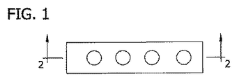
図1は、本発明のマスクの概略上面図である。
図2は、線2‐2に沿って切った側断面図である。
図3は、基板に塗工された本発明のマスクの概略上面図である。
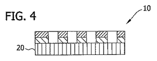
図4は、線3‐3に沿って切った側断面図である。
図5は、本発明のマスクの使用の略図である。
図6および図7は、基板に塗工された本発明のマスクの写真である。
図8および図9は、マスク中の孔に析出したはんだ金属粒子を有する図6および図7のマスクおよび基板の写真である。
図10は、本発明のマスクの写真である。
図11は、PWB基板に塗工された本発明のマスクの写真である。
図12は、図11のマスクの開口部中へのはんだ粉末析出物の写真である。
BRIEF DESCRIPTION OF THE DRAWINGS FIG. 1 is a schematic top view of a mask of the present invention.
FIG. 2 is a side sectional view taken along line 2-2.
FIG. 3 is a schematic top view of the mask of the present invention coated on a substrate.
FIG. 4 is a side sectional view taken along line 3-3.
FIG. 5 is a schematic illustration of the use of the mask of the present invention.
6 and 7 are photographs of the mask of the present invention coated on a substrate.
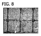
FIGS. 8 and 9 are photographs of the mask and substrate of FIGS. 6 and 7 having solder metal particles deposited in the holes in the mask.
FIG. 10 is a photograph of the mask of the present invention.
FIG. 11 is a photograph of the mask of the present invention coated on a PWB substrate.
FIG. 12 is a photograph of the solder powder deposit in the opening of the mask of FIG.
好ましい実施態様の詳細な説明
本発明の製品は、非電導性の基板上、ならびに非電導性の表面および点在する導電性の表面(例えば、20%未満の導電性の表面)を有する基板上での動電学的な析出およびパターニングを伴う方法に使用するためのマスクである。米国公開公報第2005/0106329の動電学的な方法と著しく対照的に、これらの基板は、全部または少なくとも大部分が非電導性の表面を有するガラス、ポリマー、セラミック、半導体および積層板を含む。
DETAILED DESCRIPTION OF PREFERRED EMBODIMENTS Products of the present invention are on non-conductive substrates and on substrates having non-conductive surfaces and interspersed conductive surfaces (eg, less than 20% conductive surfaces). And a mask for use in methods involving electrokinetic deposition and patterning. In marked contrast to the electrokinetic method of US Publication No. 2005/0106329, these substrates include glass, polymers, ceramics, semiconductors and laminates, all or at least mostly non-conductive surfaces. .
このマスクおよび方法は、基板上また特に非電導性の基板上でパターンにより粒子を析出することが望ましい多種多様な製造作業において、粒子の析出に適用できる。これらの用途は、表示装置技術(ガラス、プラスチック、パターニング用リン(III)などの表面上の導電性および絶縁性の配線)、印刷された電子部品(はんだ付け可能な表面/はんだ付け可能な保護層、導体、誘電体、受動素子など)、医療用(パターニング分析化学薬品、薬品投与手段など)、パラレル・アセンブリー工程(RFID金型、電子部品など)およびその他を含むがそれらに限定されない。 The mask and method can be applied to particle deposition in a wide variety of manufacturing operations where it is desirable to deposit particles by pattern on a substrate, and particularly on a non-conductive substrate. These applications include display device technologies (glass, plastic, conductive and insulating wiring on surfaces such as patterning phosphorus (III)), printed electronic components (solderable surface / solderable protection) Layers, conductors, dielectrics, passive elements, etc.), medical (patterning analysis chemicals, drug delivery means, etc.), parallel assembly processes (RFID molds, electronic components, etc.) and others, but are not limited thereto.
本発明の1つの態様においては、米国特許出願番号第10/888,286号(公開公報番号第2005/010632号)における動電学的な析出と同様の方法により析出を行い、その開示の全体が参照により明示的に本書に組み込まれる。しかしながら本発明は、本発明が、基板と対向電極との間ではなく、マスク層と対向電極の間に電位を生じさせるという点で、先行する方法からの発展である。従って本発明は、本発明が基板自体上ではなくマスク上にある粒子のための引力という点を伴うということで、一層の発展である。また、そのマスクは、基板表面と結合した埋没電極および対向電極を伴うその他の析出方法に適用できる。 In one aspect of the present invention, precipitation is performed by a method similar to electrokinetic deposition in US patent application Ser. No. 10 / 888,286 (Publication No. 2005/010632), the entire disclosure Is expressly incorporated herein by reference. However, the present invention is a development from the previous method in that the present invention generates a potential between the mask layer and the counter electrode, not between the substrate and the counter electrode. Thus, the present invention is a further development in that the present invention involves an attractive force for particles that are on the mask rather than on the substrate itself. The mask can also be applied to other deposition methods involving buried electrodes and counter electrodes coupled to the substrate surface.
本発明の前記の方法は、広い範囲の寸法の金属粒子を析出するのに適している。1つの取組みにおいて、粒子は、典型的には約2乃至約100μmの平均粒径を有する粉末である。別の取組みにおいて、粒子は、約50乃至約500μmの平均粒径を有するような中規模の粒子である。別の取組みにおいて、粒子は、約100μm乃至約1mmまたは約300μm乃至約1mmといった少なくとも約100μmの平均直径を有するような比較的大きな球体である。球体の利点は、粉末の概ね50%の密度に対して、球体が100%の密度であることである。また球体は、大量の粉末が行い得るよりも微細なピッチで析出することができ、それは、等容積の粉末よりも良好に球体が画定されることができるからであり、また、より小さい球体を使用して、より大容量の粉末と同量のはんだをリフロー後に生じさせることができるからである。球体ではまた、マスク孔が析出高さよりもずっと浅い場合、上述の単一のマスク技術を容易にする。 The method of the invention is suitable for depositing metal particles with a wide range of dimensions. In one approach, the particles are typically a powder having an average particle size of about 2 to about 100 μm. In another approach, the particles are medium sized particles having an average particle size of about 50 to about 500 μm. In another approach, the particles are relatively large spheres having an average diameter of at least about 100 μm, such as from about 100 μm to about 1 mm or from about 300 μm to about 1 mm. The advantage of spheres is that the spheres are 100% dense compared to the roughly 50% density of the powder. Also, the spheres can be deposited with a finer pitch than a large amount of powder can do, because the spheres can be defined better than an equal volume of powder, and the smaller spheres This is because it can be used to produce the same amount of solder as the larger powder after reflow. The sphere also facilitates the single mask technique described above when the mask holes are much shallower than the deposition height.
析出のための粒子の調製は、粒子への電荷の付与を必要とし、これが粒子を動電学的に動きやすくする。この基準が満たされれば、調整方法は、本発明に不可欠でない。粒子は、当技術分野で説明されているように、また以下の例証的、非限定的かつ非網羅的な代替方法に従って、調製することができる。例えば、Sn合金はんだ粉末被覆のため、ウィスコンシン州(米国)スタデヴァントのジョンソン・ポリマーLLC(Johnson Polymer,LLC)から入手することができるジョンクリル(Joncryl)682レジンを20%の濃度までメタノール中で溶解し、次に、ドイツ国ポツダムのウエルコ(Welco)有限責任会社から入手するタイプ6のSn63Pb37はんだに対し吹付被覆することができる。吹付けは、ウィスコンシン州(米国)ヴェローナのコーティング・プレイス・インク(Coating Place,Inc.)が行うワルスター法(Wurster Process)により達成される。次に、例として、トナーの調製のため、被覆された粉末(120g)を1.4リットルのビーカー中の1リットルのアイソパーGに添加し、ニュージャージー州(米国)ヒルサイドのヴィクトリー・エンジニアリング(Victory Engineering)から入手可能である「ザ・アジテイター(TheAgitator)」などの適切なミキサーにより攪拌する。磁性攪拌子は、粉末から被覆をはがすため、使用しない。電荷ディレクター(21滴、−1滴あたり0.016ml)を混合物に添加し、攪拌を少なくとも4時間継続する。トナーは、室温で2日間寝かせておく。トナーは、安定した反応を維持するため、高湿度環境(>60%RH)から保護する。 Preparation of particles for precipitation requires the application of charge to the particles, which makes the particles easier to move electrokinetically. If this criterion is met, the adjustment method is not essential to the present invention. The particles can be prepared as described in the art and according to the following illustrative, non-limiting and non-exhaustive alternative methods. For example, for a Sn alloy solder powder coating, a Johncrill 682 resin, available from Johnson Polymer, LLC of Stadevant, Wisconsin (USA), is dissolved in methanol to a concentration of 20%. It can then be spray coated onto a type 6 Sn63Pb37 solder obtained from a Welco limited liability company in Potsdam, Germany. Spraying is accomplished by the Wurster process (Coating Place, Inc.) of Verona, Wisconsin (USA). Next, by way of example, for toner preparation, the coated powder (120 g) is added to 1 liter of Isopar G in a 1.4 liter beaker and Victory Engineering, Hillside, NJ (USA). ) With a suitable mixer, such as “The Agitator” available from. A magnetic stirrer is not used because it removes the coating from the powder. Charge director (21 drops, 0.016 ml per drop) is added to the mixture and stirring is continued for at least 4 hours. The toner is allowed to sleep for 2 days at room temperature. The toner is protected from high humidity environments (> 60% RH) to maintain a stable reaction.
前述の電荷ディレクターの調製のため、例えば、コネティカット州(米国)、ミドルベリーのクロンプトン・コーポレーション(Crompton Corporation)から入手することができるバリウム・ペトロネート(barium petronate)(10g)を、200mlビーカー中で、テキサス州(米国)ヒューストンのエクソンモービル・ケミカル・カンパニーから入手することができるアイソパーG(90g)に添加する。ビーカーを熱せられた攪拌プレート上に置き、80‐90℃の温度に達するまで加熱/攪拌する。高度に精製された水(10g)、すなわち極めて純粋な蒸留水を1回に1滴(約16マイクロリットル)添加する一方、溶液を継続的に攪拌および加熱する。全ての水を添加した後、溶液をさらに1時間攪拌および加熱する。次に熱を除去し、溶液が冷えるまで攪拌を継続する。黄褐色の沈澱物の形成が認められる。混合物は、室温で1日寝かし、次に濾過し沈殿物を除去する。 For the preparation of the aforementioned charge director, for example, barium petronate (10 g), available from Crompton Corporation, Middlebury, Connecticut (USA), in a 200 ml beaker, Add to Isopar G (90 g), available from ExxonMobil Chemical Company, Houston, Texas (USA). Place the beaker on a heated stir plate and heat / stir until a temperature of 80-90 ° C is reached. Highly purified water (10 g), ie very pure distilled water, is added one drop (about 16 microliters) at a time while the solution is continuously stirred and heated. After all the water has been added, the solution is stirred and heated for an additional hour. The heat is then removed and stirring is continued until the solution cools. The formation of a tan precipitate is observed. The mixture is aged at room temperature for 1 day and then filtered to remove the precipitate.
他の実施形態における粒子を調製するため、イオン性表面活性剤材料、非イオン性ポリマーなどの非イオン性材料、有機酸および/または塩基ならびにそれらの混合物から選択する材料で粒子を被覆する。被覆が物理的にどのように行われるかにより、被覆媒体は、溶媒を含んでもよい。すなわち、溶液中の浸漬、溶液による吹付けまたは流動層中の溶液への暴露により被覆を達成する場合、溶媒を必要とする。一方、プラズマ被覆法または同様の方法により被覆を達成する場合、溶媒は要求されない。本発明に従って粒子を被覆するのに適している表面活性剤材料の中には、米国特許公報第2005/0100735号で開示されたものがある。 To prepare the particles in other embodiments, the particles are coated with a material selected from ionic surfactant materials, nonionic materials such as nonionic polymers, organic acids and / or bases and mixtures thereof. Depending on how the coating is physically performed, the coating medium may contain a solvent. That is, a solvent is required when coating is achieved by immersion in solution, spraying with solution, or exposure to solution in a fluidized bed. On the other hand, no solvent is required when coating is achieved by plasma coating or similar methods. Among the surfactant materials suitable for coating particles according to the present invention are those disclosed in US Patent Publication No. 2005/0100735.
前記の被覆材料は、被覆された粒子が電荷ディレクターによる処理に影響を受けるようにし、その結果、粒子を電荷ディレクターにより処理し、粒子を動電学的に動きやすくすることができる。この被覆は、例えば、強い水酸基性の表面または強い酸性の表面として特徴付けられる表面を提供し、これにより、次に塗工される電荷ディレクターが反応することができる。被覆材料を選択するにあたり、粒子がはんだとして使用される金属粒子である場合、はんだとして使用されるときの最終的な粉末中でフラックス機能を提供するものを選択することが好ましい。 The coating material allows the coated particles to be affected by the treatment by the charge director, so that the particles can be treated by the charge director and the particles can be moved electrokinetically. This coating provides, for example, a surface characterized as a strongly hydroxylic surface or a strongly acidic surface so that the next applied charge director can react. In selecting the coating material, if the particles are metal particles used as solder, it is preferable to select one that provides a flux function in the final powder when used as solder.
この変形における粒子は、粒子本体;電荷ディレクター材料の粒子本体への付着を促進する粒子本体上の上述の被覆媒体であって、ここで被覆媒体がアニオン種、非イオン種、カチオン種、酸、塩基およびそれらの混合物からなる群から選択されるもの;ならびに、被覆材料上の上述の電荷ディレクター材料であって、ここで電荷ディレクター材料が正または負の電荷を有し、それにより粒子本体を動電学的に動きやすくするものから構成される。 The particles in this variant are the particle body; the above-described coating medium on the particle body that promotes the adhesion of the charge director material to the particle body, wherein the coating medium is an anionic species, a nonionic species, a cationic species, an acid, Selected from the group consisting of bases and mixtures thereof; and the charge director material described above on the coating material, wherein the charge director material has a positive or negative charge, thereby moving the particle body. It consists of things that make it easier to move electronically.
上記のとおり本発明の方法において粒子を使用するため、電荷ディレクターとしても知られる電解質または高分子電解質を含む溶液に粒子を注入する。適切な電解質および高分子電解質の実施例は、前述の公報で開示されたものを含むがそれらに限定されない。このことは、それにより、析出方法において使用するため動電学的に動きやすい粒子を生じる。 To use the particles in the method of the invention as described above, the particles are injected into a solution containing an electrolyte or polyelectrolyte, also known as a charge director. Examples of suitable electrolytes and polyelectrolytes include, but are not limited to, those disclosed in the aforementioned publications. This thereby yields particles that are electrokinetically mobile for use in the deposition process.
その後、鍋乾燥、吹付乾燥またはその他の適切な手段により、粒子を乾燥する。電解質または高分子電解質の役割は、粒子が望ましい動電学的方法で反応するよう、電荷の維持を容易にすることである。 Thereafter, the particles are dried by pan drying, spray drying or other suitable means. The role of the electrolyte or polyelectrolyte is to facilitate charge maintenance so that the particles react in the desired electrokinetic manner.
析出に備えて、粒子は結合され、適切な誘電性能を有する液体で濡らされる。該液体の1つの実施例は、アイソパー製品である。別の実施例は、フロリナート(Fluorinert)の商品名を有する3−Mコーポレーションから入手することができる製品である。結合した粒子および液体の範囲は、約2重量%の粒子から約90重量%の粒子に及ぶ。粒子は、容積基準により、混合物の約2乃至60%を構成する。 In preparation for deposition, the particles are combined and wetted with a liquid having appropriate dielectric performance. One example of the liquid is an isopar product. Another example is a product available from 3-M Corporation having the trade name Fluorinert. The range of bound particles and liquids ranges from about 2% by weight particles to about 90% by weight particles. The particles make up about 2-60% of the mixture by volume.
本発明に従ってマスクが用いられ、これが、a)動電学的な析出に必要な電気接続、およびb)析出された材料から多様な構造を形成するためのパターニングを提供する。図1および図2中のマスク10は、誘電体材料である第1の層12、および導電体である第2の層14を有する。第1の層として好ましい材料には、エポキシ樹脂積層板などの乾燥フォト・レジスト・フィルムがある。第2の層すなわち導電層14として好ましい材料には、ステンレス鋼、ニッケル、アルミニウム、モリブデンおよびクロムがある。マスクは、基板上にパターニングを提供する開口部16を有する。マスクは、ここでは単純化のため、1列のみの開口部を有するものとして示す;しかし、典型的には、図6および図7で示すように、多くのそのような列を有する。
A mask is used in accordance with the present invention, which provides a) the electrical connections necessary for electrokinetic deposition, and b) patterning to form a variety of structures from the deposited material. The
マスクは、積層、接着、回転被覆、浸漬被覆により、またはスクリーン印刷と同様のステンシルを通じて、導電性材料14上に誘電体材料12を被覆することにより調製することができる。開口部16は、誘電体の塗工の前に導電性材料上にあってもよく、さもなければ、誘電体による被覆後に孔をあけることができる。
The mask can be prepared by coating the
1つの実施形態において、導電層14は、マスクの誘電層を形作る非導電性の被覆12により上塗りされる。非導電性の被覆12は、エポキシ樹脂積層板などの乾燥フォト・レジスト・フィルムでもよい。この被覆12は、1つの実施形態において、画像形成材を含みえる。たとえばそれは、アクリルを主材料とし、ポリイミドを主材料とし、市販のエポキシを主材料とするPWBはんだマスク被覆、および各種の市販の有機画像形成性のフォトポリマー被覆から選択することができる。適切なポリマーの1つは、AZPDP100XTの名称で入手することができる厚膜スピンオン光電性ポリマー、またはノヴァラック(novalac)を主材料とするAZPLP−100であり、いずれもニュージャージー州ブリッジウォーターのクラリアント(Clariant)から入手可能である。別のポリマーは、フタレックス(Futurrex)の商標で入手可能なポリスチレンを主材料とする材料である。この被覆(マスクの誘電層12)は、シリコン・ウエハのはんだバンプのため、例えば、約1μm乃至約250μmなど、少なくとも約1μmの厚さである。導電層14は、例えば、約50μm乃至約1cmの厚さである。
In one embodiment, the
マスク10は、供給者の規格により要求される場合、誘電層12を形成するポリマーを硬化させるため、例えばボックス・オーブンにおいて硬化にかけられる。
The
図3および図4に示す方法を行うにあたり、マスク10は、析出された粒子を受け取る基板20の表面上に置かれる。図5に図式的に示すように、析出される粒子24を含む容器34中の溶液28の中にマスクされた表面を浸漬する。マスク10の導電層14と溶液中に浸漬された対向電極26との間に電源30による電圧を加える。
In performing the method shown in FIGS. 3 and 4, the
電界の影響下で、溶液中の荷電粒子24は、導電層14の露出した領域に引き付けられ、そうして基板20上に析出し、マスク10中の開口部16を充填する。析出後、融解、焼結または硬化(熱、UV、触媒)により、粒子を基板に融合させることができる。
Under the influence of the electric field, the charged
本発明に従って析出する粒子は、金属、金属合金、ポリマーおよびその他の有機物、セラミック、半導体および無機化合物を含む。例えば、析出する粒子は、前記の米国特許公開公報番号第2005/0106329号および出願番号第10/888,619号(公開公報番号第2005/0100735号)において開示されたものを含むがそれらに限定されず、その開示全体が参照により明示的に本書に組み込まれる。本発明に従って、粒子が電荷ディレクターによる処理による影響を受けるようにするため、有機物または無機物の粒子を被覆し、その結果、粒子をそれにより動電学的または静電気的に動きやすくさせることができる。1つの好ましい実施形態において、粒子は、Sn、Sn/Pb、Sn/Ag/Cu、Sn/Ag、Cu、Sn/Ag/Bi、Sn/Bi、Sn/Pb/Biまたはその他の金属/合金から選択される。例えば上記のSnを主材料とする粒子およびその他の粒子など、この方法により析出される粒子の特徴は、ナノ粉末、μm・サイズの丸い粉末、300μmまでの大型粒子およびその他を含む。 The particles deposited according to the present invention include metals, metal alloys, polymers and other organics, ceramics, semiconductors and inorganic compounds. For example, precipitated particles include, but are not limited to, those disclosed in the aforementioned US Patent Publication No. 2005/0106329 and Application No. 10 / 888,619 (Publication No. 2005/0100735). Rather, the entire disclosure is expressly incorporated herein by reference. In accordance with the present invention, organic or inorganic particles can be coated so that the particles are affected by the treatment by the charge director, so that the particles can thereby be moved electrokinetically or electrostatically. In one preferred embodiment, the particles are from Sn, Sn / Pb, Sn / Ag / Cu, Sn / Ag, Cu, Sn / Ag / Bi, Sn / Bi, Sn / Pb / Bi or other metals / alloys. Selected. For example, the characteristics of the particles deposited by this method, such as the above-mentioned particles mainly composed of Sn and other particles, include nano-powder, [mu] m-sized round powder, large particles up to 300 [mu] m, and others.
本発明の方法を行うにあたり、図5に示すように、析出される粒子24の懸濁液28の中に、適用されたマスクを有する基板を浸漬する。マスクの導電性の表面14は、電極として働き、基板に隣接して、浸漬された対向電極26が存在する。30による電位が2個の電極の間に加えられ、荷電粒子を基板に向かわせる。正確な液相導電性および粒子の電荷対質量比を提供するよう、懸濁液の性質を設計する。画像コントラストが得られるのは、粒子がマスク上の導電層14に加えられた電位に引き付けられ、マスクの誘電体の表面12には引き付けられないためである。マスク上の電荷は、マスク材料への電解質を通じた電荷担体の移動により、蓄積する。
In carrying out the method of the present invention, as shown in FIG. 5, a substrate having an applied mask is immersed in a
析出の駆動力は、主として、マスクの導電層14に印加される電位の逆帯電の電気極性と荷電粒子が引き合うことにある。導電層14を電気接続に取り付けて、導電層と対向電極26との間に電位が加えられる。基板を粒子懸濁液(動電学的な溶液)28の中に浸漬する。懸濁液中で浸漬された対向電極26で、電気回路が完成される。この図5で示す懸濁液の上面に対して基板が垂直的に配列する配置が、1つの実施形態として好ましいものである。
The driving force for deposition is mainly that the charged particles are attracted to the reversely charged electric polarity of the potential applied to the
粒子が負の化学的電荷を有するよう処理する場合は、マスク10の導電層14を正極とする電位をマスクと対向電極26との間に加える。代替的に、粒子を正の電荷を有するよう処理する場合は、マスク10の導電層14を陰極とする電位をマスクの導電層に加える。例えば、回路の負端子を懸濁液中の対向電極板に取り付け、正端子をマスクの導電層に取り付ける。さもなければ、回路の正端子を懸濁液中の対向電極に取り付け、負端子をマスクの導電層に取り付ける。
When the particles are treated so as to have a negative chemical charge, a potential having the
懸濁液28の中の荷電粒子24は、導電層14に引き付けられ、導電層14は、粒子上の電荷と反対の極性の端子として設定される。荷電粒子は、マスクの導電層と対向電極との間の電位により生じた電界を通じて移動する。電極と電圧源の反対の極に取り付けられた対向電極がそれらの間に電位を生じさせることにより、粒子は、マスクの導電性の部分に隣接する基板のマスクされていない部分上の孔16中に動電学的に析出する。この実施形態において、マスクの誘電層12にコロナ電荷を加える必要はない。マスクは、機械的かつ静電気的な障壁として機能する。静電荷は、電解質を通じた担体の流れによりマスクの誘電層12上に蓄積し、これが電界を形作り、これが電気的にマスク中の孔の中へと荷電粒子を進ませる。
The charged
この方法は、例えば50+/−50V乃至500+/−500VのAC電位による単一の析出段階を伴う。代替的な実施形態は、析出を引き起こすためにマスクの導電層と対向電極との間に加えられた電位を変えることを伴う。1つの実施形態において、これは、析出の全部または一部の期間において緩慢に上昇する電圧の掃引またはランプを伴う。別の実施形態において、これは、より段階的な方法による電位の増加を伴う。例えば、これは、約50+/−50V乃至約500+/−500Vの電位における第1段階の析出;ならびに、約200+/−200乃至約300+/−300Vの電位における第2および第3段階の析出を行うことを伴う。これらの3回の反復は、a)凹部の底への充填;b)凹部の上、さらには非導電層の上までの凹部の充填;およびc)既に析出された粒子の上部への過剰充填を伴う3段階の析出に概ね相当する。他の実施形態は、2回乃至数回の範囲の3以外の数の繰り返しによる変形を用いる。この段階的析出は、マスク孔の充填がより整然としているため、析出をより高密度とし、空隙または閉鎖をより少なくすると思われる。 This method involves a single deposition step, for example with an AC potential of 50 +/− 50V to 500 +/− 500V. An alternative embodiment involves changing the potential applied between the conductive layer of the mask and the counter electrode to cause deposition. In one embodiment, this involves a voltage sweep or ramp that rises slowly during all or part of the deposition. In another embodiment, this involves increasing the potential in a more gradual manner. For example, this may involve first stage deposition at a potential of about 50 +/− 50V to about 500 +/− 500V; and second and third stage deposition at a potential of about 200 +/− 200 to about 300 +/− 300V. With doing. These three iterations consist of a) filling the bottom of the recess; b) filling the recess over the recess and even the top of the non-conductive layer; and c) overfilling the top of the already deposited particles. This generally corresponds to a three-stage precipitation accompanied by Other embodiments use variations with a number of repetitions other than 3 ranging from 2 to several times. This gradual deposition is likely to result in a denser deposition and fewer voids or closures due to the more ordered mask hole filling.
析出方法の他のパラメーターに関して、電位は、正弦波として、またはより好ましくは鋸歯状波として、加えられる。周波数は、約10乃至1000Hz、好ましくは約50乃至500Hz、より好ましくは約75乃至150Hzである。析出のための時間は、約2乃至30秒の範囲、例えば約5乃至約20秒の範囲であり、または1つの具体的な実施形態において約8乃至約15秒の範囲である。基板と対向電極の間の距離は、1つの実施形態において、約5乃至約6mmである。一般命題として、この距離は、約3乃至約10mm、最も典型的には、約4乃至約7−mmである。 With respect to other parameters of the deposition method, the potential is applied as a sine wave, or more preferably as a sawtooth wave. The frequency is about 10 to 1000 Hz, preferably about 50 to 500 Hz, more preferably about 75 to 150 Hz. The time for deposition is in the range of about 2 to 30 seconds, such as in the range of about 5 to about 20 seconds, or in one specific embodiment in the range of about 8 to about 15 seconds. The distance between the substrate and the counter electrode is about 5 to about 6 mm in one embodiment. As a general proposition, this distance is about 3 to about 10 mm, most typically about 4 to about 7-mm.
特定の理論に拘束されることなく、基板の最深の機構上における金属粒子の初期の析出の間、比較的弱い電位は、電位がより強い場合よりも少ない粒子が導電層14に引き付けられる結果をもたらし、短い時間に機構の中へ非常に多くの粒子を密集させる可能性を減少させると考えられる。電位が初期においてより強い場合、粒子は、機構中に激しく密集し、基板に対してくぼみ開口部を閉鎖し、または過剰な空隙をもたらす可能性がある。初期においてより弱い電位は、それほど激しくなく移動し、その結果、多数の粒子が非導電層中のくぼみに同時に入るよう強いられることなく、粒子が基板上にしっかりと納まることが可能トナーる。
Without being bound by a particular theory, during the initial deposition of metal particles on the deepest mechanism of the substrate, a relatively weak potential results in fewer particles being attracted to the
適切な滞留時間の後、基板は、溶液の上面に対して平行とならないよう、垂直または一定の角度で除去される。1つの好ましい実施形態において、基板は、除去の間、垂直面から約15乃至約75度の角度にある。静電モードに関連して上述した基板の振動が、動電学的モードに関連して有利であることも認められた。 After an appropriate residence time, the substrate is removed at a vertical or constant angle so that it is not parallel to the top surface of the solution. In one preferred embodiment, the substrate is at an angle of about 15 to about 75 degrees from the vertical plane during removal. It has also been observed that the vibration of the substrate described above in relation to the electrostatic mode is advantageous in relation to the electrokinetic mode.
析出後、基板は選択的に、析出された粒子を含むマスク開口部を下向きにして、すすぎ溶液中の短時間の浸漬により洗浄される。これは、析出と同一の容器中におけるその場での洗浄によっても行うことができ、これは、同時に行われる懸濁液の除去と粒子を含まないすすぎ溶液との交換を要する。 After deposition, the substrate is optionally cleaned by brief immersion in a rinse solution with the mask opening containing the deposited particles facing down. This can also be done by in situ cleaning in the same container as the precipitation, which requires simultaneous removal of the suspension and replacement with a particle-free rinse solution.
次に、選択的に、析出された粒子に対し静電気クランプを付与するため、基板をコロナ電荷にあてることができる。特に、例えば5乃至7キロボルトの電位を有するコロナ発生器が、コロナ電荷を付与するため基板上を通過する。これは、マスクに加えられた静電気力により、粒子をしかるべき場所に保持するのに役立つ。 Next, the substrate can be subjected to a corona charge to selectively apply an electrostatic clamp to the deposited particles. In particular, a corona generator having a potential of, for example, 5 to 7 kilovolts passes over the substrate to impart a corona charge. This helps to keep the particles in place by the electrostatic forces applied to the mask.
懸濁液中の溶媒の性質に応じて、典型的には30℃乃至60℃の範囲の上昇した温度に基板を曝すことにより、残存溶媒を完全に乾かす。これにより、はんだ粉末粒子を表面上に有する、図9で図解した種類の基板が生じる。 Depending on the nature of the solvent in the suspension, the residual solvent is completely dried by exposing the substrate to an elevated temperature, typically in the range of 30 ° C to 60 ° C. This results in a substrate of the type illustrated in FIG. 9 having solder powder particles on the surface.
従って、説明したように、本発明は、導電層14、誘電層12およびマスク開口部16を有するマスク10を基板に塗工して、マスク開口部16が形作るマスクされていない表面を有するマスクされた基板を生じること;荷電粒子24を含む溶液28中にマスクされた基板を浸漬すること、ならびに、マスクの導電層14と対向電極26との間に電位30を生じさせ、それによりマスク開口部16中の導電層14上の露出した表面に荷電粒子24を動電学的に引き付け、マスク開口部16中に荷電粒子を析出させることからなる、荷電粒子24のパターンを基板に塗工することを含む。
Thus, as described, the present invention applies a
次に例えば、標準的なマルチゾーンはんだリフロー炉、または好ましくは、低酸素(<100ppm、より好ましくは<20ppm)リフロー炉に置くことにより、はんだをリフローする。基板を下から熱することが好ましい。リフローの間、金属粒子上の被覆は、フラックスとして機能する。吹付けられた液体フラックスを用いるといった付随的なフラックス塗工も、リフローを促進するため使用することができる。マスクは除去され、これにより、表面上にはんだバンプを有する基板が生じる。 The solder is then reflowed, for example by placing it in a standard multi-zone solder reflow furnace, or preferably in a low oxygen (<100 ppm, more preferably <20 ppm) reflow furnace. It is preferable to heat the substrate from below. During reflow, the coating on the metal particles functions as a flux. Additional flux coatings such as using sprayed liquid flux can also be used to facilitate reflow. The mask is removed, resulting in a substrate having solder bumps on the surface.
異なる方法による本発明のマスクを使用した一層の変形においては、別の印刷ツールが使用され、本発明のマスクは、その印刷ツールに対し、粒子がその中で基板に移転するパターンを形作る。この印刷ツールは、平坦な表面を有する絶縁支持体であり、基板20の代わりに平坦なツール表面が使用されることを除き、図4で示すものと同様のマスクがそのツールに適用される。典型的な印刷ツールは、ポリイミドやエポキシなどの材料から構成され、約1乃至約200μmの厚さと、直径が約1cm乃至約100cmの範囲のツール表面寸法を有する。
In a further variation using the mask of the present invention by a different method, another printing tool is used, which forms a pattern for the printing tool in which particles are transferred to the substrate. The printing tool is an insulating support having a flat surface and a mask similar to that shown in FIG. 4 is applied to the tool except that a flat tool surface is used instead of the
表面上にマスク10を有するツールを粒子と液体の混合物に浸し、マスクの導電層と対向電極との間に電位を加えると、その結果、マスクが保護していないツールの部分上すなわち孔16に粒子が集められる。この方法において、ツール表面は、誘電性流体中で粒子に曝され、この粒子は電気化学的電荷を有し、それによりツール表面上のマスクされていない領域上に大量の粒子を析出させ、それによりマスクされていない領域上の粒子によりパターン化されたツール表面を生じる。遊離した粒子は、純粋な誘電性の液体媒体の塗工により、ツールからすすがれる。この方法は特に、少なくとも約100μm、例えば約100μm乃至約1mmの平均直径を有する金属球体に対して行うときに好結果をもたらす。
When a tool having a
粒子がツールからそこに移転するシリコン・ウエハまたはその他の基板は、誘電性流体で前もって濡らしておくことにより準備する。基板は、完全に接地した支持体に取り付ける。 A silicon wafer or other substrate onto which particles are transferred from the tool is prepared by prewetting with a dielectric fluid. The substrate is attached to a fully grounded support.
付着した粒子を有するパターン化されたツール表面を電子素子またはその他の基板の表面にしっかりと触れさせ、それにより、パターン化されたツール表面上のパターンが形作る基板パターンによりパターン化されたツール表面からの粒子の量の少なくとも一部を基板の表面に移転することにより、基板への移転は達成される。1つの実施形態においてこれを達成するため、荷電しすすがれたツールをパターン化される基板表面上に配置し、約20μm乃至約300μmの間隙が基板をツール表面から分離する。ツールと比較してより低い基板の電荷電位により、粒子は基板に移転し、粒子がツール表面に形作ったのと同一のパターンを保持する。代替的に、マスクの導電層に加えられた電位をこの時点で変更して、基板への移転を促進することができる。あるいは、基板自体が導電性である場合、該移転を促進する電位を基板に加えることができる。 From the tool surface patterned by the substrate pattern that the patterned tool surface with attached particles touches the surface of the electronic device or other substrate, thereby forming a pattern on the patterned tool surface. Transfer to the substrate is achieved by transferring at least a portion of the amount of particles to the surface of the substrate. To accomplish this in one embodiment, a charged and rinsed tool is placed on the substrate surface to be patterned, and a gap of about 20 μm to about 300 μm separates the substrate from the tool surface. The lower substrate charge potential compared to the tool causes the particles to move to the substrate and retain the same pattern that the particles have shaped on the tool surface. Alternatively, the potential applied to the conductive layer of the mask can be changed at this point to facilitate transfer to the substrate. Alternatively, if the substrate itself is conductive, a potential that promotes the transfer can be applied to the substrate.
次に、誘電性流体を基板から蒸発させる。例えば、リフロー温度まで基板およびはんだを熱するため炉の中で基板を焼くことを伴う従来のはんだリフロー技術により、はんだは溶解し基板に融合する。 Next, the dielectric fluid is evaporated from the substrate. For example, the solder melts and fuses to the substrate by conventional solder reflow techniques that involve baking the substrate in a furnace to heat the substrate and solder to the reflow temperature.
非導電性の積層板を基板として用いる。はんだマスクで被覆された銅層であり125μmの直径の開口部を有するマスクを調製する。図6および図7は、適用されたマスクを有する基板を例示したものである。析出は、アイソパー、120g/lの前処理されたはんだ粉末、および0.5mlの10%バリウム・ペトロネート溶液を含む溶液を用いて、国際公開公報 WO2005/033352号で説明されたのと同様のトナー中で行われる。適用されたマスクを有する基板を、対向電極を有する溶液中に浸漬する。銅層と対向電極の間に200Vの電圧を加える。20秒後、マスク中の析出開口部は、はんだ粉末により充填される。図8および図9は、はんだ粉末粒子の析出後の基板を示す。 A non-conductive laminate is used as the substrate. A mask is prepared which is a copper layer covered with a solder mask and has an opening with a diameter of 125 μm. 6 and 7 illustrate a substrate having an applied mask. Precipitation is similar to that described in International Publication No. WO 2005/033352 using a solution containing Isopar, 120 g / l pre-treated solder powder, and 0.5 ml of 10% barium petronate solution. Done in. The substrate having the applied mask is immersed in a solution having a counter electrode. A voltage of 200 V is applied between the copper layer and the counter electrode. After 20 seconds, the deposition openings in the mask are filled with solder powder. 8 and 9 show the substrate after the deposition of solder powder particles.
エポキシ樹脂積層板を有するステンレス鋼導電層からなるマスクを、図10で示すパターンで、上記の手順により調製した。マスクは、図11に示すPWB基板の上に置かれた。上記の手順によりマスクの開口部中にはんだ粉末が析出し、図12に示す基板上に、はんだ粒子を生じた。これは、狭いピッチ間隔と広い配線幅で析出させることが可能な本発明の能力を説明する。 A mask made of a stainless steel conductive layer having an epoxy resin laminate was prepared by the above procedure with the pattern shown in FIG. The mask was placed on the PWB substrate shown in FIG. By the above procedure, solder powder was deposited in the opening of the mask, and solder particles were generated on the substrate shown in FIG. This explains the ability of the present invention to deposit with narrow pitch spacing and wide wiring width.
主として基板に金属粒子を塗工する文脈で本発明の方法および材料を上で説明したが、その方法および材料は、粒子の性質が電気化学的電荷を付与され得るものであることを条件として、非金属粒子の析出にも適用することができる。非金属粉末を伴うそのような方法の実施例は、例えば、平面パネル型表示装置などに使用するための燐光体、ガラス、セラミック、半導体材料の析出を含む。 While the methods and materials of the present invention have been described above primarily in the context of applying metal particles to a substrate, the methods and materials are subject to the fact that the nature of the particles can be imparted with an electrochemical charge. It can also be applied to the precipitation of non-metallic particles. Examples of such methods involving non-metallic powders include, for example, the deposition of phosphors, glasses, ceramics, and semiconductor materials for use in flat panel displays and the like.
本発明の要素またはその好ましい実施形態を紹介するとき、冠詞「一つの(a,an)」、「その(the)」および「上記の(said)」は、1または複数の要素が存在することを意味するよう意図する。「からなる(comprising)」、「含む(including)」および「有する(having)」の用語は、包含的であり、列挙された要素以外の追加の要素が存在し得ることを意味するよう意図する。 When introducing an element of the present invention or a preferred embodiment thereof, the articles “a”, “the” and “said” may include one or more elements. Is meant to mean The terms “comprising”, “including” and “having” are intended to be inclusive and mean that there may be additional elements other than the listed elements. .
本発明の範囲から逸脱せずに上記に様々の変更を行うことができるため、上記の説明に含まれ添付の図面に示される全ての事項は、包含的であり限定的な意味でないと解釈されるよう意図する。前記は、説明目的のみのために提供された限られた数の実施例に関する。本発明の範囲が添付された請求により決定されることが意図されており、本発明の範囲から逸脱しない上記の実施例の変更が存在する。 Since various modifications can be made to the above without departing from the scope of the present invention, all matters contained in the above description and shown in the accompanying drawings are intended to be inclusive and not limiting. I intend to. The foregoing relates to a limited number of embodiments provided for illustrative purposes only. It is intended that the scope of the invention be determined by the appended claims, and that there are modifications to the embodiments described above that do not depart from the scope of the invention.
10 マスク
12 第1の層
14 第2の層
16 開口部
20 基板
10
Claims (9)
導電層、絶縁層、および前記導電層および絶縁層を貫通するマスク開口部を有するマスクを基板に、基板と絶縁層の間のマスク部に導電層が位置するように配置し、マスク開口部が形成するマスクされていない表面を有するマスクされた基板を生じること;
荷電粒子を含む溶液中にマスクされた基板を浸漬すること;ならびに、
前記マスクの導電層と対向電極との間に電位を生じさせ、それによりマスク開口部中の導電層上の露出した表面に荷電粒子を動電学的に引き付け、マスク開口部中および基板上に荷電粒子を析出させること;
析出後、融解、焼結、または熱、UVまたは触媒の手段による硬化により、荷電粒子を基板に融合させること。 A method of applying a pattern of charged particles to a substrate comprising:
A conductive layer, an insulating layer, and a mask having a mask opening penetrating the conductive layer and the insulating layer are arranged on the substrate so that the conductive layer is located in the mask portion between the substrate and the insulating layer, and the mask opening is Producing a masked substrate having an unmasked surface to form;
Immersing the masked substrate in a solution containing charged particles; and
An electric potential is generated between the conductive layer of the mask and the counter electrode, thereby attracting charged particles electrokinetically to the exposed surface on the conductive layer in the mask opening, in the mask opening and on the substrate Depositing charged particles ;
After deposition, the charged particles are fused to the substrate by melting, sintering, or curing by means of heat, UV or catalyst .
導電層、絶縁層、および前記導電層および絶縁層を貫通するマスク開口部を有するマスクを非導電性の基板に、基板と絶縁層の間のマスク部に導電層が位置するように配置し、マスク開口部が形成するマスクされていない表面を有するマスクされた非導電性の基板を生じること;
荷電粒子を含む溶液中にマスクされた非導電性の基板を浸漬すること;ならびに、
マスクの導電層と対向電極との間に電位を生じさせ、それによりマスク開口部中の導電層上の露出した表面に荷電粒子を動電学的に引き付け、マスク開口部中および非導電性の基板上に荷電粒子を析出させること;
析出後、融解、焼結、または熱、UVまたは触媒の手段による硬化により、荷電粒子を基板に融合させること。 A method for applying a pattern of charged particles to a non-conductive substrate comprising:
A conductive layer, an insulating layer, and a mask having a mask opening penetrating the conductive layer and the insulating layer are arranged on a non-conductive substrate so that the conductive layer is located in a mask portion between the substrate and the insulating layer, Producing a masked non-conductive substrate having an unmasked surface formed by a mask opening;
Immersing the masked non-conductive substrate in a solution containing charged particles; and
An electric potential is generated between the conductive layer of the mask and the counter electrode, thereby attracting charged particles electrokinetically to the exposed surface on the conductive layer in the mask opening, and in the mask opening and non-conductive Depositing charged particles on the substrate ;
After deposition, the charged particles are fused to the substrate by melting, sintering, or curing by means of heat, UV or catalyst .
Applications Claiming Priority (3)
| Application Number | Priority Date | Filing Date | Title |
|---|---|---|---|
| US68213005P | 2005-05-18 | 2005-05-18 | |
| US60/682,130 | 2005-05-18 | ||
| PCT/US2006/019250 WO2006125089A2 (en) | 2005-05-18 | 2006-05-18 | Mask and method for electrokinetic deposition and patterning process on substrates |
Publications (3)
| Publication Number | Publication Date |
|---|---|
| JP2008546182A JP2008546182A (en) | 2008-12-18 |
| JP2008546182A5 JP2008546182A5 (en) | 2009-07-16 |
| JP5301269B2 true JP5301269B2 (en) | 2013-09-25 |
Family
ID=37432143
Family Applications (1)
| Application Number | Title | Priority Date | Filing Date |
|---|---|---|---|
| JP2008512507A Expired - Fee Related JP5301269B2 (en) | 2005-05-18 | 2006-05-18 | Masks and methods for electrokinetic deposition and patterning processes on substrates |
Country Status (6)
| Country | Link |
|---|---|
| US (1) | US7678255B2 (en) |
| EP (1) | EP1882056A2 (en) |
| JP (1) | JP5301269B2 (en) |
| KR (1) | KR20080022111A (en) |
| TW (1) | TWI388697B (en) |
| WO (1) | WO2006125089A2 (en) |
Families Citing this family (8)
| Publication number | Priority date | Publication date | Assignee | Title |
|---|---|---|---|---|
| US7538429B2 (en) * | 2006-08-21 | 2009-05-26 | Intel Corporation | Method of enabling solder deposition on a substrate and electronic package formed thereby |
| US8216441B2 (en) * | 2007-12-10 | 2012-07-10 | Applied Materials, Inc. | Electrophoretic solar cell metallization process and apparatus |
| US8323998B2 (en) * | 2009-05-15 | 2012-12-04 | Achrolux Inc. | Methods and apparatus for forming uniform layers of phosphor material on an LED encapsulation structure |
| KR101104681B1 (en) * | 2010-01-08 | 2012-01-16 | 서울대학교산학협력단 | Method for adhering charged particles on non-conductive substrates |
| CN103030097B (en) * | 2012-12-12 | 2015-06-17 | 中北大学 | Method for preparing wafer level low-dimensional nanostructures based on electrostatic field self-focusing |
| US20170301434A1 (en) * | 2016-04-18 | 2017-10-19 | Littelfuse, Inc. | Methods for manufacturing an insulated busbar |
| US10685766B2 (en) | 2016-04-18 | 2020-06-16 | Littelfuse, Inc. | Methods for manufacturing an insulated busbar |
| CN107723753B (en) * | 2017-09-27 | 2021-04-27 | 上海瑞尔实业有限公司 | Preparation method of high-strength high-toughness nickel metal shielding tool |
Family Cites Families (21)
| Publication number | Priority date | Publication date | Assignee | Title |
|---|---|---|---|---|
| US3431887A (en) | 1963-11-13 | 1969-03-11 | Polymer Corp | Apparatus for coating articles in a fluidized bed |
| JPH04211193A (en) * | 1990-03-22 | 1992-08-03 | Canon Inc | Conductive circuit member and its manufacture, conductive paste, and electronic equipment |
| US5981043A (en) | 1996-04-25 | 1999-11-09 | Tatsuta Electric Wire And Cable Co., Ltd | Electroconductive coating composition, a printed circuit board fabricated by using it and a flexible printed circuit assembly with electromagnetic shield |
| US5817374A (en) * | 1996-05-31 | 1998-10-06 | Electrox Corporation | Process for patterning powders into thick layers |
| CA2572503A1 (en) | 1997-04-04 | 1998-10-15 | University Of Southern California | Method for electrochemical fabrication including enhanced data manipulation |
| TWI231293B (en) | 1997-11-12 | 2005-04-21 | Jsr Corp | Transfer film |
| US6153348A (en) | 1998-08-07 | 2000-11-28 | Parelec Llc | Electrostatic printing of conductors on photoresists and liquid metallic toners therefor |
| US6781612B1 (en) | 1998-10-13 | 2004-08-24 | Electrox Corporation | Electrostatic printing of functional toner materials for electronic manufacturing applications |
| AU1799401A (en) | 1999-11-23 | 2001-06-04 | Electrox Corporation | A durable electrostatic printing plate and method of making the same |
| US6524758B2 (en) | 1999-12-20 | 2003-02-25 | Electrox Corporation | Method of manufacture of printed wiring boards and flexible circuitry |
| TW495809B (en) * | 2000-02-28 | 2002-07-21 | Semiconductor Energy Lab | Thin film forming device, thin film forming method, and self-light emitting device |
| JP2004527814A (en) | 2000-12-15 | 2004-09-09 | エレクトロックス コーポレイション | Method for manufacturing a new cheap radio frequency identification device |
| JP2002223059A (en) * | 2001-01-24 | 2002-08-09 | Sharp Corp | Method for forming fine pattern |
| WO2002063397A1 (en) | 2001-02-08 | 2002-08-15 | Electrox Corp. | An improved electrostatic printing plate possessing a tiered surface |
| WO2002071465A1 (en) | 2001-03-02 | 2002-09-12 | Electrox Corp. | Process for the manufacture of large area arrays of discrete components |
| US6803092B2 (en) * | 2001-06-26 | 2004-10-12 | 3M Innovative Properties Company | Selective deposition of circuit-protective polymers |
| US6790483B2 (en) | 2002-12-06 | 2004-09-14 | Eastman Kodak Company | Method for producing patterned deposition from compressed fluid |
| US6780249B2 (en) | 2002-12-06 | 2004-08-24 | Eastman Kodak Company | System for producing patterned deposition from compressed fluid in a partially opened deposition chamber |
| US7413771B2 (en) | 2003-07-09 | 2008-08-19 | Fry's Metals, Inc. | Coating solder metal particles with a charge director medium |
| US7585549B2 (en) | 2003-07-09 | 2009-09-08 | Fry's Metals, Inc. | Method of applying a pattern of particles to a substrate |
| JP2007277619A (en) * | 2006-04-05 | 2007-10-25 | Electroplating Eng Of Japan Co | Method of depositing particle according to electrophoresis |
-
2006
- 2006-05-18 WO PCT/US2006/019250 patent/WO2006125089A2/en active Application Filing
- 2006-05-18 JP JP2008512507A patent/JP5301269B2/en not_active Expired - Fee Related
- 2006-05-18 EP EP06760104A patent/EP1882056A2/en not_active Withdrawn
- 2006-05-18 KR KR1020077029468A patent/KR20080022111A/en not_active Application Discontinuation
- 2006-05-18 TW TW095117708A patent/TWI388697B/en not_active IP Right Cessation
- 2006-05-18 US US11/419,128 patent/US7678255B2/en active Active
Also Published As
| Publication number | Publication date |
|---|---|
| WO2006125089A3 (en) | 2007-11-22 |
| US7678255B2 (en) | 2010-03-16 |
| JP2008546182A (en) | 2008-12-18 |
| US20060260943A1 (en) | 2006-11-23 |
| WO2006125089A2 (en) | 2006-11-23 |
| EP1882056A2 (en) | 2008-01-30 |
| TWI388697B (en) | 2013-03-11 |
| TW200706704A (en) | 2007-02-16 |
| KR20080022111A (en) | 2008-03-10 |
Similar Documents
| Publication | Publication Date | Title |
|---|---|---|
| JP5301269B2 (en) | Masks and methods for electrokinetic deposition and patterning processes on substrates | |
| TWI395256B (en) | Deposition and patterning process | |
| US8318595B2 (en) | Self-assembled electrical contacts | |
| JP4741616B2 (en) | Method for forming photoresist laminated substrate | |
| TWI328416B (en) | Multi-layer printed circuit board and method for fabricating the same | |
| EP2745658B1 (en) | Method of forming a conductive image on a non-conductive surface | |
| JP2006503176A (en) | Electrochemically molded and hermetically sealed microstructure and method and apparatus for producing the microstructure | |
| CN107043953A (en) | Electroplate the durable low solidification temperature hydrophobic coating in cup assembly | |
| DE102009050426B3 (en) | Method for aligned application of silicon chips with switching structures on e.g. wafer substrate, involves fixing aligned components on substrate by electrostatic force by applying electrical holding voltage above metallization surfaces | |
| EP1996002B1 (en) | Bump forming method and bump forming apparatus | |
| WO2007122868A1 (en) | Method for forming bump and device for forming bump | |
| TWI232717B (en) | Solder supply method, solder bump using said method, formation method and device for said solder-coating film | |
| US8393077B2 (en) | Fabrication of passive electronic components | |
| WO2006017327A2 (en) | Electrocodeposition of lead free tin alloys | |
| US20080035710A1 (en) | Solder Composition and Solder Layer Forming Method Using the Same | |
| US8308887B2 (en) | Via hole forming method using electrophotographic printing method | |
| WO2006008736A1 (en) | Fabrication of electrical components and circuits by selective electrophoretic deposition (s-epd) and transfer | |
| US5340617A (en) | Electrostatic patterning of multi-layer module lamina | |
| JPH08315946A (en) | Connecting method and connecting device of base | |
| JP2004022963A (en) | Method for connecting part and method and apparatus for mounting part using the same | |
| US8304150B1 (en) | Electrostatic printing of functional toner materials for the construction of useful micro-structures | |
| JP2011171604A (en) | Method of manufacturing electronic component, electronic component manufacturing apparatus, and photoresist | |
| JP2002223059A (en) | Method for forming fine pattern | |
| JP2001007484A (en) | Formation method for conductor pattern | |
| JP2003046222A (en) | Bonding material and its manufacturing method |
Legal Events
| Date | Code | Title | Description |
|---|---|---|---|
| A621 | Written request for application examination |
Free format text: JAPANESE INTERMEDIATE CODE: A621 Effective date: 20090518 |
|
| A521 | Request for written amendment filed |
Free format text: JAPANESE INTERMEDIATE CODE: A523 Effective date: 20090521 |
|
| A131 | Notification of reasons for refusal |
Free format text: JAPANESE INTERMEDIATE CODE: A131 Effective date: 20110802 |
|
| A521 | Request for written amendment filed |
Free format text: JAPANESE INTERMEDIATE CODE: A523 Effective date: 20111102 |
|
| A131 | Notification of reasons for refusal |
Free format text: JAPANESE INTERMEDIATE CODE: A131 Effective date: 20120522 |
|
| A601 | Written request for extension of time |
Free format text: JAPANESE INTERMEDIATE CODE: A601 Effective date: 20120821 |
|
| A602 | Written permission of extension of time |
Free format text: JAPANESE INTERMEDIATE CODE: A602 Effective date: 20120828 |
|
| A521 | Request for written amendment filed |
Free format text: JAPANESE INTERMEDIATE CODE: A523 Effective date: 20120919 |
|
| A131 | Notification of reasons for refusal |
Free format text: JAPANESE INTERMEDIATE CODE: A131 Effective date: 20121127 |
|
| A521 | Request for written amendment filed |
Free format text: JAPANESE INTERMEDIATE CODE: A523 Effective date: 20130125 |
|
| TRDD | Decision of grant or rejection written | ||
| A01 | Written decision to grant a patent or to grant a registration (utility model) |
Free format text: JAPANESE INTERMEDIATE CODE: A01 Effective date: 20130521 |
|
| A61 | First payment of annual fees (during grant procedure) |
Free format text: JAPANESE INTERMEDIATE CODE: A61 Effective date: 20130619 |
|
| R150 | Certificate of patent or registration of utility model |
Ref document number: 5301269 Country of ref document: JP Free format text: JAPANESE INTERMEDIATE CODE: R150 Free format text: JAPANESE INTERMEDIATE CODE: R150 |
|
| R250 | Receipt of annual fees |
Free format text: JAPANESE INTERMEDIATE CODE: R250 |
|
| R250 | Receipt of annual fees |
Free format text: JAPANESE INTERMEDIATE CODE: R250 |
|
| R250 | Receipt of annual fees |
Free format text: JAPANESE INTERMEDIATE CODE: R250 |
|
| R250 | Receipt of annual fees |
Free format text: JAPANESE INTERMEDIATE CODE: R250 |
|
| R250 | Receipt of annual fees |
Free format text: JAPANESE INTERMEDIATE CODE: R250 |
|
| LAPS | Cancellation because of no payment of annual fees |