JP5290574B2 - Schottky device - Google Patents
Schottky device Download PDFInfo
- Publication number
- JP5290574B2 JP5290574B2 JP2007515097A JP2007515097A JP5290574B2 JP 5290574 B2 JP5290574 B2 JP 5290574B2 JP 2007515097 A JP2007515097 A JP 2007515097A JP 2007515097 A JP2007515097 A JP 2007515097A JP 5290574 B2 JP5290574 B2 JP 5290574B2
- Authority
- JP
- Japan
- Prior art keywords
- schottky
- region
- transistor
- terminal
- well region
- Prior art date
- Legal status (The legal status is an assumption and is not a legal conclusion. Google has not performed a legal analysis and makes no representation as to the accuracy of the status listed.)
- Expired - Fee Related
Links
- 239000002184 metal Substances 0.000 claims description 22
- 229910052751 metal Inorganic materials 0.000 claims description 22
- 239000000758 substrate Substances 0.000 claims description 13
- 238000002955 isolation Methods 0.000 claims description 12
- 239000004065 semiconductor Substances 0.000 claims description 5
- 229910017052 cobalt Inorganic materials 0.000 claims description 2
- 239000010941 cobalt Substances 0.000 claims description 2
- GUTLYIVDDKVIGB-UHFFFAOYSA-N cobalt atom Chemical compound [Co] GUTLYIVDDKVIGB-UHFFFAOYSA-N 0.000 claims description 2
- 229910021332 silicide Inorganic materials 0.000 claims description 2
- FVBUAEGBCNSCDD-UHFFFAOYSA-N silicide(4-) Chemical compound [Si-4] FVBUAEGBCNSCDD-UHFFFAOYSA-N 0.000 claims description 2
- 230000015556 catabolic process Effects 0.000 description 23
- 238000000034 method Methods 0.000 description 12
- 230000008901 benefit Effects 0.000 description 8
- 230000000694 effects Effects 0.000 description 6
- 230000008569 process Effects 0.000 description 6
- 230000004888 barrier function Effects 0.000 description 4
- 238000010586 diagram Methods 0.000 description 3
- 230000006872 improvement Effects 0.000 description 3
- 238000009413 insulation Methods 0.000 description 3
- XUIMIQQOPSSXEZ-UHFFFAOYSA-N Silicon Chemical compound [Si] XUIMIQQOPSSXEZ-UHFFFAOYSA-N 0.000 description 2
- 230000001066 destructive effect Effects 0.000 description 2
- 238000012986 modification Methods 0.000 description 2
- 230000004048 modification Effects 0.000 description 2
- 229910052710 silicon Inorganic materials 0.000 description 2
- 239000010703 silicon Substances 0.000 description 2
- 238000006731 degradation reaction Methods 0.000 description 1
- 239000007943 implant Substances 0.000 description 1
- 230000010354 integration Effects 0.000 description 1
- 239000000463 material Substances 0.000 description 1
- 230000009467 reduction Effects 0.000 description 1
- 230000000630 rising effect Effects 0.000 description 1
Images


Classifications
-
- H—ELECTRICITY
- H01—ELECTRIC ELEMENTS
- H01L—SEMICONDUCTOR DEVICES NOT COVERED BY CLASS H10
- H01L27/00—Devices consisting of a plurality of semiconductor or other solid-state components formed in or on a common substrate
- H01L27/02—Devices consisting of a plurality of semiconductor or other solid-state components formed in or on a common substrate including semiconductor components specially adapted for rectifying, oscillating, amplifying or switching and having at least one potential-jump barrier or surface barrier; including integrated passive circuit elements with at least one potential-jump barrier or surface barrier
- H01L27/04—Devices consisting of a plurality of semiconductor or other solid-state components formed in or on a common substrate including semiconductor components specially adapted for rectifying, oscillating, amplifying or switching and having at least one potential-jump barrier or surface barrier; including integrated passive circuit elements with at least one potential-jump barrier or surface barrier the substrate being a semiconductor body
- H01L27/06—Devices consisting of a plurality of semiconductor or other solid-state components formed in or on a common substrate including semiconductor components specially adapted for rectifying, oscillating, amplifying or switching and having at least one potential-jump barrier or surface barrier; including integrated passive circuit elements with at least one potential-jump barrier or surface barrier the substrate being a semiconductor body including a plurality of individual components in a non-repetitive configuration
- H01L27/07—Devices consisting of a plurality of semiconductor or other solid-state components formed in or on a common substrate including semiconductor components specially adapted for rectifying, oscillating, amplifying or switching and having at least one potential-jump barrier or surface barrier; including integrated passive circuit elements with at least one potential-jump barrier or surface barrier the substrate being a semiconductor body including a plurality of individual components in a non-repetitive configuration the components having an active region in common
- H01L27/0705—Devices consisting of a plurality of semiconductor or other solid-state components formed in or on a common substrate including semiconductor components specially adapted for rectifying, oscillating, amplifying or switching and having at least one potential-jump barrier or surface barrier; including integrated passive circuit elements with at least one potential-jump barrier or surface barrier the substrate being a semiconductor body including a plurality of individual components in a non-repetitive configuration the components having an active region in common comprising components of the field effect type
- H01L27/0727—Devices consisting of a plurality of semiconductor or other solid-state components formed in or on a common substrate including semiconductor components specially adapted for rectifying, oscillating, amplifying or switching and having at least one potential-jump barrier or surface barrier; including integrated passive circuit elements with at least one potential-jump barrier or surface barrier the substrate being a semiconductor body including a plurality of individual components in a non-repetitive configuration the components having an active region in common comprising components of the field effect type in combination with diodes, or capacitors or resistors
-
- H—ELECTRICITY
- H01—ELECTRIC ELEMENTS
- H01L—SEMICONDUCTOR DEVICES NOT COVERED BY CLASS H10
- H01L27/00—Devices consisting of a plurality of semiconductor or other solid-state components formed in or on a common substrate
- H01L27/02—Devices consisting of a plurality of semiconductor or other solid-state components formed in or on a common substrate including semiconductor components specially adapted for rectifying, oscillating, amplifying or switching and having at least one potential-jump barrier or surface barrier; including integrated passive circuit elements with at least one potential-jump barrier or surface barrier
- H01L27/04—Devices consisting of a plurality of semiconductor or other solid-state components formed in or on a common substrate including semiconductor components specially adapted for rectifying, oscillating, amplifying or switching and having at least one potential-jump barrier or surface barrier; including integrated passive circuit elements with at least one potential-jump barrier or surface barrier the substrate being a semiconductor body
- H01L27/06—Devices consisting of a plurality of semiconductor or other solid-state components formed in or on a common substrate including semiconductor components specially adapted for rectifying, oscillating, amplifying or switching and having at least one potential-jump barrier or surface barrier; including integrated passive circuit elements with at least one potential-jump barrier or surface barrier the substrate being a semiconductor body including a plurality of individual components in a non-repetitive configuration
- H01L27/0611—Devices consisting of a plurality of semiconductor or other solid-state components formed in or on a common substrate including semiconductor components specially adapted for rectifying, oscillating, amplifying or switching and having at least one potential-jump barrier or surface barrier; including integrated passive circuit elements with at least one potential-jump barrier or surface barrier the substrate being a semiconductor body including a plurality of individual components in a non-repetitive configuration integrated circuits having a two-dimensional layout of components without a common active region
- H01L27/0617—Devices consisting of a plurality of semiconductor or other solid-state components formed in or on a common substrate including semiconductor components specially adapted for rectifying, oscillating, amplifying or switching and having at least one potential-jump barrier or surface barrier; including integrated passive circuit elements with at least one potential-jump barrier or surface barrier the substrate being a semiconductor body including a plurality of individual components in a non-repetitive configuration integrated circuits having a two-dimensional layout of components without a common active region comprising components of the field-effect type
- H01L27/0629—Devices consisting of a plurality of semiconductor or other solid-state components formed in or on a common substrate including semiconductor components specially adapted for rectifying, oscillating, amplifying or switching and having at least one potential-jump barrier or surface barrier; including integrated passive circuit elements with at least one potential-jump barrier or surface barrier the substrate being a semiconductor body including a plurality of individual components in a non-repetitive configuration integrated circuits having a two-dimensional layout of components without a common active region comprising components of the field-effect type in combination with diodes, or resistors, or capacitors
-
- H—ELECTRICITY
- H01—ELECTRIC ELEMENTS
- H01L—SEMICONDUCTOR DEVICES NOT COVERED BY CLASS H10
- H01L29/00—Semiconductor devices adapted for rectifying, amplifying, oscillating or switching, or capacitors or resistors with at least one potential-jump barrier or surface barrier, e.g. PN junction depletion layer or carrier concentration layer; Details of semiconductor bodies or of electrodes thereof ; Multistep manufacturing processes therefor
- H01L29/66—Types of semiconductor device ; Multistep manufacturing processes therefor
- H01L29/86—Types of semiconductor device ; Multistep manufacturing processes therefor controllable only by variation of the electric current supplied, or only the electric potential applied, to one or more of the electrodes carrying the current to be rectified, amplified, oscillated or switched
- H01L29/861—Diodes
-
- H—ELECTRICITY
- H01—ELECTRIC ELEMENTS
- H01L—SEMICONDUCTOR DEVICES NOT COVERED BY CLASS H10
- H01L29/00—Semiconductor devices adapted for rectifying, amplifying, oscillating or switching, or capacitors or resistors with at least one potential-jump barrier or surface barrier, e.g. PN junction depletion layer or carrier concentration layer; Details of semiconductor bodies or of electrodes thereof ; Multistep manufacturing processes therefor
- H01L29/02—Semiconductor bodies ; Multistep manufacturing processes therefor
- H01L29/06—Semiconductor bodies ; Multistep manufacturing processes therefor characterised by their shape; characterised by the shapes, relative sizes, or dispositions of the semiconductor regions ; characterised by the concentration or distribution of impurities within semiconductor regions
- H01L29/0603—Semiconductor bodies ; Multistep manufacturing processes therefor characterised by their shape; characterised by the shapes, relative sizes, or dispositions of the semiconductor regions ; characterised by the concentration or distribution of impurities within semiconductor regions characterised by particular constructional design considerations, e.g. for preventing surface leakage, for controlling electric field concentration or for internal isolations regions
- H01L29/0642—Isolation within the component, i.e. internal isolation
- H01L29/0649—Dielectric regions, e.g. SiO2 regions, air gaps
- H01L29/0653—Dielectric regions, e.g. SiO2 regions, air gaps adjoining the input or output region of a field-effect device, e.g. the source or drain region
-
- H—ELECTRICITY
- H01—ELECTRIC ELEMENTS
- H01L—SEMICONDUCTOR DEVICES NOT COVERED BY CLASS H10
- H01L29/00—Semiconductor devices adapted for rectifying, amplifying, oscillating or switching, or capacitors or resistors with at least one potential-jump barrier or surface barrier, e.g. PN junction depletion layer or carrier concentration layer; Details of semiconductor bodies or of electrodes thereof ; Multistep manufacturing processes therefor
- H01L29/40—Electrodes ; Multistep manufacturing processes therefor
- H01L29/402—Field plates
-
- H—ELECTRICITY
- H01—ELECTRIC ELEMENTS
- H01L—SEMICONDUCTOR DEVICES NOT COVERED BY CLASS H10
- H01L29/00—Semiconductor devices adapted for rectifying, amplifying, oscillating or switching, or capacitors or resistors with at least one potential-jump barrier or surface barrier, e.g. PN junction depletion layer or carrier concentration layer; Details of semiconductor bodies or of electrodes thereof ; Multistep manufacturing processes therefor
- H01L29/66—Types of semiconductor device ; Multistep manufacturing processes therefor
- H01L29/68—Types of semiconductor device ; Multistep manufacturing processes therefor controllable by only the electric current supplied, or only the electric potential applied, to an electrode which does not carry the current to be rectified, amplified or switched
- H01L29/76—Unipolar devices, e.g. field effect transistors
- H01L29/772—Field effect transistors
- H01L29/78—Field effect transistors with field effect produced by an insulated gate
- H01L29/7838—Field effect transistors with field effect produced by an insulated gate without inversion channel, e.g. buried channel lateral MISFETs, normally-on lateral MISFETs, depletion-mode lateral MISFETs
-
- H—ELECTRICITY
- H01—ELECTRIC ELEMENTS
- H01L—SEMICONDUCTOR DEVICES NOT COVERED BY CLASS H10
- H01L29/00—Semiconductor devices adapted for rectifying, amplifying, oscillating or switching, or capacitors or resistors with at least one potential-jump barrier or surface barrier, e.g. PN junction depletion layer or carrier concentration layer; Details of semiconductor bodies or of electrodes thereof ; Multistep manufacturing processes therefor
- H01L29/66—Types of semiconductor device ; Multistep manufacturing processes therefor
- H01L29/86—Types of semiconductor device ; Multistep manufacturing processes therefor controllable only by variation of the electric current supplied, or only the electric potential applied, to one or more of the electrodes carrying the current to be rectified, amplified, oscillated or switched
- H01L29/861—Diodes
- H01L29/872—Schottky diodes
Description
本発明は半導体に関連し、特にショットキー・ダイオードのように動作することができる半導体デバイスに関連する。 The present invention relates to semiconductors, and more particularly to semiconductor devices that can operate like Schottky diodes.
ショットキー・ダイオードはかなりの数の適応例で利用できることが長い間に見出されてきた。ショットキー・ダイオードは順バイアス方向において、様々な便利な機能を提供するPN接合ダイオードよりも低閾値を有する。典型的なショットキー・ダイオードの一つの重要な不利益は、逆バイアス方向における漏れ電流が、逆バイアス電圧の増加に従い指数的に増加することである。この効果は時には「障壁低下」と呼ばれる。一般的に改善が望まれる他の特性は、ブレークダウン電圧である。ショットキー・ダイオードのI−V特性曲線は図1に示される。これは片対数目盛であり、電圧(V)は線型の目盛で、電流(I)は対数の目盛である。これは電流が逆バイアス電圧に伴い指数的に(対数プロットで直線的に)増加することを示し、且つブレークダウン電圧(BV)が存在することを示す。このブレークダウン電圧は、バックグラウンドのドーピング濃度を減少させることにより50ボルトほど増加させることができるが、このことは順方向バイアス電流を減少させる。同様にして、逆バイアス電圧を伴う漏れ電流の指数的増加のために、ブレークダウン電圧に近づくにつれ、漏れ電流は非常に大きくなる。 It has long been found that Schottky diodes can be used in a considerable number of applications. Schottky diodes have a lower threshold in the forward bias direction than PN junction diodes that provide various convenient functions. One important disadvantage of typical Schottky diodes is that the leakage current in the reverse bias direction increases exponentially with increasing reverse bias voltage. This effect is sometimes called “barrier lowering”. Another characteristic that is generally desired to improve is breakdown voltage. The IV characteristic curve of the Schottky diode is shown in FIG. This is a semi-logarithmic scale, the voltage (V) is a linear scale, and the current (I) is a logarithmic scale. This indicates that the current increases exponentially (linearly in a logarithmic plot) with the reverse bias voltage, and that there is a breakdown voltage (BV). This breakdown voltage can be increased by as much as 50 volts by reducing the background doping concentration, which reduces the forward bias current. Similarly, because of the exponential increase in leakage current with reverse bias voltage, the leakage current becomes very large as the breakdown voltage is approached.
このことを改善するために、ショットキー・ダイオードの両側で高密度なドープ領域を利用する技術が、障壁低下効果を「ピンチオフ」するために開発されてきた。この技術には障壁低下を実質的に消去する効果及びブレークダウン電圧を改善する効果もある。このアプローチに伴う問題として、処理が単純ではないこと、及びショットキー・ダイオードの大きさが大幅に増大することがあげられる。非常に一直線で垂直な障壁を有する深く且つ高濃度なドープ領域を必要とするものが垂直的解決策である。これは達成困難な組み合わせであり、例え努力する価値があると考えられるときでも、深いコンタクトに依存する。絶縁処理及び離散処理のような垂直性を有する処理は、このピンチオフを達成するために必要な段階を加えてより修正することが可能である。CMOS及び混合信号処理のようなより水平な他の処理は、更にいっそうの困難を被り、ショットキー・ダイオードの改善を達成するためにピンチオフ・タイプの集積を試みるときにより費用がかかる。 In order to remedy this, techniques that utilize high density doped regions on both sides of the Schottky diode have been developed to "pinch off" the barrier lowering effect. This technique also has the effect of substantially eliminating the barrier drop and improving the breakdown voltage. The problems with this approach are that the process is not simple and the size of the Schottky diode is greatly increased. A vertical solution is one that requires a deep and heavily doped region with a very straight vertical barrier. This is a difficult combination to achieve and relies on deep contact even when it is considered worth the effort. Processes with verticality, such as isolation and discrete processes, can be further modified with the steps necessary to achieve this pinch-off. Other more horizontal processes such as CMOS and mixed signal processing suffer even more and are more expensive when attempting pinch-off type integration to achieve Schottky diode improvements.
従って、漏れ及び/且つブレークダウン電圧を改善したショットキーデバイスであって、水平処理でより単純に利用できるものへの需要が存在する。 Therefore, there is a need for Schottky devices with improved leakage and / or breakdown voltage that can be used more simply in horizontal processing.
本発明は、例示する方法により説明され、添付される図面により制限されない。図面において、近い参照番号は類似する構成要素を示す。
図面における構成要素は単純性及び明快性を有するよう説明され、縮尺どおりに描かれる必要は無いことに、当業者は気づく。例えば、図面中のいくつかの構成要素の寸法は、本発明の実施形態の理解を助長するために他の構成要素に比べて比較的誇張されてもよい。
The present invention is illustrated by way of example and is not limited by the accompanying drawings. In the drawings, close reference numbers indicate similar components.
Those skilled in the art will realize that the components in the drawings are described as having simplicity and clarity and need not be drawn to scale. For example, the dimensions of some components in the drawings may be relatively exaggerated relative to other components to facilitate an understanding of embodiments of the present invention.
一態様において、ショットキー・ダイオード特性及びMOSトランジスタを有する原理的なショットキー・ダイオード又はデバイスは直列に結合されて、順電流がわずかに劣化するだけで漏れ電流及びブレークダウン電圧の大幅な改善をもたらす。逆バイアスの場合、小さな逆バイアス電流は存在するが、MOSトランジスタによりショットキー・ダイオードにかかる電圧は小さく保たれる。MOSトランジスタがブレークダウン状態になるまで、ほとんどすべての逆バイアスがMOSトランジスタにかかる。しかし、ショットキー・ダイオードが電流を制限するのでこのトランジスタのブレークダウンは始めから破壊的なわけではない。逆バイアス電圧が増加し続けるにつれて、ショットキー・ダイオードにより多くの電圧がかかり始める。このことにより漏れ電流は増加されるが、ブレークダウン電圧はトランジスタとショットキー・ダイオードとのブレークダウン電圧の間でいくらか追加される。電流が大幅に減少し、トランジスタ又はショットキー・ダイオードいずれか一つのみの場合よりも大きいブレークダウン電圧が正味の影響である。このことは、図面及び以下の記載を参照することによりより深く理解される。 In one aspect, a principle Schottky diode or device with Schottky diode characteristics and MOS transistors is coupled in series to significantly improve leakage and breakdown voltage with only a slight degradation of forward current. Bring. In the case of reverse bias, a small reverse bias current exists, but the voltage applied to the Schottky diode is kept small by the MOS transistor. Almost all reverse bias is applied to the MOS transistor until the MOS transistor is in a breakdown state. However, the breakdown of this transistor is not destructive from the beginning because the Schottky diode limits the current. As the reverse bias voltage continues to increase, more voltage begins to be applied to the Schottky diode. This increases the leakage current but adds some breakdown voltage between the breakdown voltage of the transistor and the Schottky diode. The net effect is that the current is greatly reduced and the breakdown voltage is larger than in the case of only one transistor or Schottky diode. This is better understood with reference to the drawings and the following description.
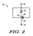
図1に示されるものは、ショットキー・ダイオード16、正端子12、負端子14、及びNチャンネル・トランジスタ18を備えるショットキーデバイス10である。本明細書で利用される記法では、ショットキーデバイスに順バイアスがかけられるときは電流は正端子12から負端子14に流れ、逆バイアスがかけられるときは漏れ電流が負端子14から正端子12に流れる。ショットキー・ダイオード16は正端子12に結合される正端子と負端子とを有する。トランジスタ18は、ショットキー・ダイオード16の負端子に端子20で接続される第一電極、正端子12に接続されるゲート、負端子14に接続される第二電極、正端子12に接続される本体、及びチャンネル領域22を有する。トランジスタ20の第一電極は、ショットキーデバイス10に順方向バイアスがかけられるときにドレインとして機能し、ショットキーデバイス10に逆方向バイアスがかけられるときにソースとして機能する。チャンネル領域22はドープされ、トランジスタ18は、例えば−0.2ボルトの負の閾値電圧を有するNチャンネルのデプリーション・モードのトランジスタとなる。この閾値電圧はこれとは違ってもよいが、好適には負であり、従って、デプリーション・モードのデバイスである。
Shown in FIG. 1 is a
順バイアスの動作において、デプリーション・モードのデバイスであるために、トランジスタ18には導電性があり、端子12の電圧は端子14の電圧よりも高い。ショットキー・ダイオード16は自然な閾値電圧において導電性を得るので、ショットキーデバイス10はショットキー・ダイオード16の閾値電圧で導電性を得る。順バイアスが増加するにつれて、トランジスタ18は幾分導電性を得るが、ショットキー・ダイオード16が通常のショットキー・ダイオードのように端子12と端子14とをクランプするので、電圧増加に伴って最小の電圧しか増加できない。順方方向バイアスの増加に従って、トランジスタ18の本体は端子12における上昇電圧に関係し、トランジスタ18の導電性に役に立つが、本体を第一電流電極に関係させることができ、デバイスはショットキー・ダイオードのようにまだ動作する。これらは、ショットキー・ダイオード16のみの場合と比べて、順バイアス電流におけるショットキーデバイス10にとっての小さな減少であり、トランジスタ18によりいくらかの抵抗が加えられたことに起因するが、このことはショットキー・ダイオードの大きさをわずかに増加させ、且つトランジスタ18の大きさを適切に調節することにより容易に保障され、所望の順電流を達成することができる。
In forward bias operation, because it is a depletion mode device,
逆バイアスの動作において、端子12と端子14との間の任意の低電圧差動において、トランジスタ18には導電性があり、ショットキー・ダイオード16にかかる電圧差動に基づいてショットキー・ダイオード16には漏れ電流が流れる。端子14の電圧が端子12の電圧に比べて増加するに従い、トランジスタ18に電圧がかかる。端子20における電圧は端子12に比べて極端に増加することができず、トランジスタ18は絶縁状態になる。従って、トランジスタ18によりショットキー・ダイオードの負端子で電圧が制限される効果がある。−0.2ボルトの閾値電圧を有するトランジスタ18のこの例では、トランジスタ18は端子20における電圧が端子12における電圧よりも約0.5〜1.0ボルト大きくなるときに絶縁される。従って、ショットキー・ダイオード16にかかる電圧は、0.5〜1.0ボルト以下に制限される。このことは、漏れ電流がショットキー・ダイオード16にかかる0.5〜1.0ボルトの逆方向バイアスに対する電流を超えることが防止され、これにより端子12及び端子14上の逆バイアス電圧がショットキー・ダイオード16にかかる場合に発生する、指数関数的な増加が回避される。
In reverse bias operation, at any low voltage differential between
図3に示されるものは、ショットキーデバイス10の逆バイアス方向におけるI−V曲線である。これはショットキー・ダイオードに関する初期電流と、次にトランジスタ18のブレークダウン電圧BTに達するまで、電流が平坦に保たれることを示す。これは、トランジスタ18がかなりの電圧を吸収し続け、その結果、ショットキー・ダイオード16は、端子12及び端子14に印加される逆バイアス電圧に比べて著しく少ない電圧で逆バイアスされるという事実によるものである。トランジスタ18がブレークダウンに達するとき、電流の増加があるが、電流がショットキー・ダイオード16により制限されるため、この点においては破壊的なブレークダウンではない。逆バイアスが増加するにつれ、電流は指数的に増加し始めるが、典型的なショットキー・ダイオードの電圧よりは非常に大きい。最終的に、ショットキーデバイス10のブレークダウン電圧BDに達する。
FIG. 3 shows an IV curve in the reverse bias direction of the
図4に示されるものは、ショットキー・ダイオード16及びトランジスタ18のショットキーデバイス10であり、P型シリコンの基板24、基板24の中のP型のウエル26、基板24の中のN型ウエル28、P+がドープされたコンタクト領域30、コンタクト領域30に隣接する素子間分離領域32、ウエル26における領域を囲み且つ素子間分離領域32に隣接する部分があるN+領域であるコンタクト20、N−がドープされ且つコンタクト20の一部に隣接するチャンネル領域22、チャンネル領域22から離れた素子間分離領域34、N+がドープされたコンタクト領域36、領域20により囲まれる部分を覆いつくす、ショットキー・ダイオード16の負端子としての金属38、チャンネル領域22及び素子間分離領域34の一部、そしてチャンネル22と素子間分離領域34との間のウエル53の一部の上方にあるゲート40、及びゲート40の下にあるゲート絶縁42を備えるデバイスの構造を備える。ゲート絶縁42及びゲート40は領域26と28の両方に重複するように設計される。コンタクト20と領域30、23、20、22、34及び36とは基板24の表面から短距離だけ下に伸びる。
Shown in FIG. 4 is a
コンタクト領域30はウエル26へのコンタクトとしての役割を果たし、ひいてはトランジスタ18及びショットキー・ダイオード16の正端子に対するコンタクトとしての役割を果たす。コンタクト20は、ショットキー・ダイオード16の従来のガードリングとしての役割、トランジスタ18の第一電極としての役割、及びショットキー・ダイオード16の負端子とトランジスタ18の第一電極との間のコンタクトとしての役割を果たす。チャンネル領域22はウエル26からウエル28に拡がる。素子間分離領域34はコンタクト領域36をチャンネル22から分離し、トランジスタ18のブレークダウン電圧を増加する。ウエル28のようなウエル本体を有するトランジスタのこのタイプの構成は、部分的にチャンネルの下にあり、ゲート40とコンタクト36との間のオフ状態において高電圧であってよい領域28は、MOSトランジスタのブレークダウン電圧を増加させるための周知の構造である。コンタクト領域36はショットキーデバイス10の負端子の接点である。
Contact region 30 serves as a contact to well 26 and thus serves as a contact to the positive terminals of
図4に示されるこのデバイスの構造により、従来のショットキー・ダイオードが従来の高ブレークダウン電圧のMOS構造に、図2の回路で達成されるように組み合わされ、集積することによるいくつかの効果を有する。これに必要な処理は当業者には周知のことであり、例えば素子分離領域34の幅及びゲート40の端からの領域36の距離などを調整することにより、このタイプの構造を利用してブレークダウン電圧は調整可能であることを当業者は認識する。本発明のこの実施形態の一有効性は、ショットキー・ダイオードの正端子コンタクト及びトランジスタ本体コンタクト両方としてコンタクト領域30を利用することにある。他の有効性は、ショットキー・ダイオードの従来のガードリングをトランジスタのドレインとして利用し、これによりまた、ショットキー・ダイオードとトランジスタとの間のコンタクトを実現することである。これらの効果により複雑な処理が導入されない。従って、このことは水平処理技術を利用して漏れ電流及びブレークダウン電圧を改善することが容易に達成でき、ピンチオフ・アプローチに必要な垂直処理技術を利用する必要が無いことは明らかである。
The structure of this device shown in FIG. 4 provides several advantages by combining and integrating a conventional Schottky diode with a conventional high breakdown voltage MOS structure as achieved in the circuit of FIG. Have The processing necessary for this is well known to those skilled in the art. For example, by adjusting the width of the
図5に示されるものは、図2の回路を実現するための別のデバイス構造50である。デバイス構造50は、P型の基板51、Pウエル52、Nウエル53、P+がドープされた領域54、領域54に隣接するN−がドープされてウエル52からウエル56まで横切る領域56及びチャンネル領域56から離れた素子分離62、N+がドープされ領域64に隣接する領域64、領域54及び56の一部の上の金属58、領域58から離れて領域52,53及び56と素子分離領域62との一部に重複するゲート60、及びゲート60の下のゲート絶縁を備える。チャンネル領域56を形成するインプラントもウエル53が受け、N+にならない程度ウエル53の表面でN型ドーピング濃度が増加する。この場合、ショットキー・ダイオードの正端子は金属58であり、負端子は金属58の下の領域56の一部である。トランジスタは、ゲート60が金属58から離されている領域56を介してショットキー・ダイオードにコンタクトする第一電極を有する。トランジスタがデプリーション・モードになることを提供するチャンネルはゲート60の下の領域56の一部である。ウエル53、領域62、及び領域64はブレークダウン電圧が増加したトランジスタを提供し、領域64はまた、ショットキーデバイス50の負端子のコンタクトをも提供する。端子57はショットキーデバイス50の正端子として金属58及びゲート60の両方にコンタクトされる。領域54は金属54を介して正端子57へトランジスタの本体へのコンタクトを提供する。従って、回路2に記載される接続は図5に示されるこの構造で満たされる。
Shown in FIG. 5 is another device structure 50 for implementing the circuit of FIG. The device structure 50 includes a P-
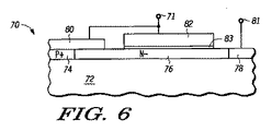
図6に示されるものは、図2の回路を形成する第二の別のショットキーデバイス70である。ショットキーデバイス70は、基板72、P+の領域74、領域74に隣接するN−の領域76、領域76に隣接するN+の領域、領域74の一部及び領域76の上の金属80、領域76の一部の上で金属80から離れたゲート82、及びゲート82の下のゲート絶縁83を備える。ゲート82は領域78から領域76により離される。ショットキーデバイス70の正端子71はゲート82及び金属80の両方に接続される。トランジスタへの本体コンタクトは端子71から金属80を通じて領域74まで、従って基板72までである。金属80はショットキー・ダイオードの正端子である。金属80の下の領域76の一部はショットキー・ダイオードの負端子である。金属80及とゲート82とが離れる領域76の部分はトランジスタの第一電極であり、且つトランジスタの第一電極とショットキー・ダイオードの負端子との間のコンタクトでもある。トランジスタのチャンネルはゲート82の下の領域76の一部である。第二電極は領域76の一部であり、領域78に隣接し且つゲート82の下ではない。ショットキーデバイス70の負端子は領域78に接続される端子81であり、領域78は代わりにトランジスタの第二電極に接続される。このアプローチは、ゲート82と領域78との間の領域76の一部に依存し、必要なブレークダウン電圧を実現する。従って、回路2に記載される接続は、図6に示されるこの構造で満たされる。
Shown in FIG. 6 is a second
本明細書において、ショットキー・ダイオードは、十分にドープされた半導体領域と接してPN接合のものよりも低い順バイアス閾値を有するダイオードが形成されるような金属領域から形成されるダイオードとなるように考慮されている。ショットキー同等のデバイスにより図1に示されるような特性曲線が示され、ショットキー同等のデバイスにはショットキー・ダイオード及び「擬ショットキー・ダイオード」と題される米国特許番号6,476,442B1号明細書のような他の構造が含まれる。ショットキーデバイスはショットキー同等のデバイス及び改良を含む構造であり、改良とはショットキー同等のデバイスの性能を改良することである。 As used herein, a Schottky diode is a diode formed from a metal region such that a diode with a forward bias threshold lower than that of a PN junction is formed in contact with a well-doped semiconductor region. Is considered. A characteristic curve as shown in FIG. 1 is shown by a Schottky equivalent device, which includes a Schottky diode and US Pat. No. 6,476,442B1 entitled “Pseudo-Schottky Diode”. Other structures such as the specification are included. A Schottky device is a structure that includes a Schottky equivalent device and improvements, where the improvement is to improve the performance of the Schottky equivalent device.
図7に示されるものは、ショットキーデバイス84の回路図であって、ショットキー・ダイオードとデプリーション・トランジスタとを組み合わせることを記載した方法でデプリーション・トランジスタと組み合わされるショットキー同等のデバイスを利用する。ショットキーデバイス84はトランジスタ90及びトランジスタ92を備える。この場合、トランジスタ90は例えば0.2ボルトを超えないが負ではない非常に低い閾値電圧を有する非デプリーション・トランジスタである。トランジスタ92はデプリーション・トランジスタである。この実施形態において、両トランジスタはNチャンネルである。トランジスタ90はショットキー同等のデバイスとして動作するように接続される。トランジスタ90は端子86に接続される第一電極を有し、ショットキーデバイス84の正端子であり、ゲートが端子86に接続され、本体が端子86に接続され、且つショットキー同等のデバイスの負端子としての第二電極である。トランジスタ90の本体、第一電極、及びゲートは互いに結合され、ショットキーデバイスの正端子として動作する。トランジスタ92はトランジスタ90の第二電極に接続される第一電極、端子86に接続されるゲート、端子86に接続される本体、及び端子88に接続される第二電極を有し、端子88はショットキーデバイス84の負端子である。
Shown in FIG. 7 is a circuit diagram of a
これまでの明細書において、本発明は特定の実施形態を参照して記載されてきた。しかし、当業者は様々な改良及び変化が以下の請求項で説明されるような本発明の範囲から逸脱せずに成され得ることを認識する。例えば、シリコンとは異なる他の半導体物質が基板として利用されてもよい。導電性は同様の結果を実現するために逆転されてもよい。ショットキー・ダイオードで利用される金属はケイ化コバルトと異なってもよい。二つのものが接続されたとして記載されてきたが、それらはまた、直結される代わりに間に何か挟まった構造により結合されてもよい。従って、明細書及び図面は制限というよりはむしろ説明と見なされるべきであり、このような全ての改良は本発明の範囲に含まれることが意図される。 In the foregoing specification, the invention has been described with reference to specific embodiments. However, one of ordinary skill in the art appreciates that various modifications and changes can be made without departing from the scope of the invention as set forth in the claims below. For example, other semiconductor materials different from silicon may be used as the substrate. The conductivity may be reversed to achieve a similar result. The metal utilized in the Schottky diode may be different from cobalt silicide. Although two have been described as connected, they may also be joined by a sandwiched structure instead of being directly connected. Accordingly, the specification and drawings are to be regarded as illustrative rather than restrictive, and all such modifications are intended to be included within the scope of the present invention.
利点、他の優位性、及び問題の解法が、特定の実施形態に関して本明細書に記載されてきた。しかし、利点、優位性、問題の解法及び任意の利点、優位性又は解法をもたらすか、又は解法をより明確にすることの要因となるかもしれない任意の要素は、任意又は全ての請求項の決定的に重要な、必要な、又は本質的な特徴又は要素として構成されるべきではない。本明細書で利用されるように、用語「備える」、「備えている」又はこの任意の活用形は非排他的包含を含むことが意図されており、要素のリストを備える処理、方法、物件、又は装置はこれらの要素を含むだけでなく、明白にリストされない又は本来備わっている処理、方法、物品又は装置のような他の要素を含んでもよい。 Benefits, other advantages, and solutions to problems have been described herein with regard to specific embodiments. However, any element that may provide an advantage, advantage, solution to the problem and any advantage, advantage or solution, or that may make the solution more explicit is that of any or all claims. It should not be configured as a critically important, necessary, or essential feature or element. As used herein, the terms “comprising”, “comprising” or any use of this are intended to include non-exclusive inclusions, processes, methods, properties comprising a list of elements Or the apparatus not only includes these elements, but may also include other elements such as processes, methods, articles or devices not explicitly listed or inherent.
Claims (4)
ショットキー・ダイオードと同等に動作するデバイスと、
前記ショットキーと同等に動作するデバイスの前記負端子(88)を形成する第一電極、前記ショットキーと同等に動作するデバイスの前記正端子(86)に接続されるゲート、及び第二電極を有するデプリーション・トランジスタ(92)と、
を備え、
前記ショットキー・ダイオードと同等に動作するデバイスは、互いに接続されるとともに、前記ショットキーと同等に動作するデバイスの前記正端子(86)を形成する第一電流電極、ゲート、及び本体と、前記デプリーション・トランジスタ(92)の前記第二電極に接続された第二電流電極とを有し、0.2ボルトを超えないが、負ではない閾値電圧を有する非デプリーション・トランジスタ(90)を含む、ショットキーと同等に動作するデバイス。 A device operating equivalently to a Schottky having a positive terminal (86) and a negative terminal (88),
A device that behaves like a Schottky diode,
A first electrode forming the negative terminal (88) of the device operating equivalent to the Schottky, a gate connected to the positive terminal (86) of the device operating equivalent to the Schottky, and a second electrode; and depletion Li Shon-transistor (92) having,
With
A device that operates equivalent to the Schottky diode is connected to each other and forms a first current electrode (86) of the device that operates equivalent to the Schottky, a gate, and a body; and and a second current electrode connected to the second electrode of the depletion Li Shon transistor (92), but does not exceed 0.2 volts, the non-depletion transistor having a threshold voltage not negative (90) Including devices that operate in the same way as Schottky.
正端子及び負端子を有するショットキー・ダイオード(16)と、
前記ショットキー・ダイオード(16)の前記負端子に接続される第一電流電極(20)、前記ショットキーデバイスの前記正端子(12)に接続されるゲート(40)、及び前記ショットキーデバイスの負端子(14)に接続される第二電流電極(36)を有するデプリーション・トランジスタ(18)と、
を備え、前記ショットキーデバイスは基板(24)の半導体領域に形成され、該基板は、
第一導電性の第一ウエル領域(26)と、
前記第一ウエル領域に隣接する第二導電性の第二ウエル領域(28)と、
前記基板の表面に位置し、前記ショットキーデバイスの前記正端子(12)に結合され、前記第一ウエル領域よりも高濃度にドープされ、且つ前記第一ウエル領域内にある、前記第一導電性である第一ドープ領域(30)と、
前記第一ウエル領域の第一部分上の金属(38)であって、前記金属は前記ショットキー・ダイオード(16)の前記負端子であり、且つ前記第一ウエル領域の前記第一部分は前記ショットキー・ダイオード(16)の前記正端子である、前記金属(38)と、
前記第一ウエル領域の前記第一部分と前記第一ドープ領域(30)との間の前記第一ウエル領域内の第一素子分離領域(32)と、
前記第一ウエル領域の前記第一部分から離間し、前記第一ウエル領域内にあり、且つ前記基板の前記表面にある前記第二導電性のチャンネル領域(22)と、
前記チャンネル領域(22)の上方にあるゲート(40)と、
前記第二導電性であり、前記デプリーション・トランジスタの前記第一電流電極であり、前記チャンネル領域(22)よりも高濃度にドープされ、且つ前記チャンネル領域(22)に隣接し且つ接続され、且つ前記金属(38)の下にあり且つ前記金属(38)に接触する少なくとも一部を有する第二ドープ領域(20)と、
前記チャンネル領域(22)から離間し、前記第二導電性であり、前記デプリーション・トランジスタの前記第二電流電極であり、前記基板の前記表面にあり、前記第二ウエル領域(28)内にあり、且つ前記ショットキーデバイスの前記負端子(14)である、第三ドープ領域(36)と、
前記チャンネル領域(22)と前記第三ドープ領域(36)との間にある第二素子分離領域(34)と、
を有する、ショットキーデバイス。 A Schottky device (10) having a positive terminal (12) and a negative terminal (14),
A Schottky diode (16) having a positive terminal and a negative terminal;
A first current electrode (20) connected to the negative terminal of the Schottky diode (16); a gate (40) connected to the positive terminal (12) of the Schottky device; and depletion Li Shon transistor having a second current electrode connected to the negative terminal (14) (36) and (18),
The Schottky device is formed in a semiconductor region of a substrate (24), the substrate comprising:
A first conductive first well region (26);
A second conductive second well region (28) adjacent to the first well region;
The first conductivity located on the surface of the substrate, coupled to the positive terminal (12) of the Schottky device, doped more heavily than the first well region, and in the first well region A first doped region (30) that is
A metal (38) on a first portion of the first well region, the metal being the negative terminal of the Schottky diode (16), and the first portion of the first well region being the Schottky The metal (38) being the positive terminal of the diode (16);
A first element isolation region (32) in the first well region between the first portion of the first well region and the first doped region (30);
The second conductive channel region (22) spaced from the first portion of the first well region, in the first well region, and on the surface of the substrate;
A gate (40) above the channel region (22);
Wherein a second electrically conductive, said first current electrode of the depletion Li Shon transistor than said channel region (22) heavily doped, is and adjacent to and connected to said channel region (22) And a second doped region (20) having at least a portion underlying said metal (38) and in contact with said metal (38);
Spaced from the channel region (22), the second conductive, the second current electrode of the depletion transistor, on the surface of the substrate and in the second well region (28) And a third doped region ( 36 ) that is the negative terminal (14) of the Schottky device;
A second element isolation region (34) between the channel region (22) and the third doped region ( 36 );
Having a Schottky device.
Applications Claiming Priority (3)
| Application Number | Priority Date | Filing Date | Title |
|---|---|---|---|
| US10/856,602 | 2004-05-28 | ||
| US10/856,602 US7071518B2 (en) | 2004-05-28 | 2004-05-28 | Schottky device |
| PCT/US2005/014323 WO2005119913A2 (en) | 2004-05-28 | 2005-04-26 | Schottky device |
Publications (3)
| Publication Number | Publication Date |
|---|---|
| JP2008501238A JP2008501238A (en) | 2008-01-17 |
| JP2008501238A5 JP2008501238A5 (en) | 2008-06-19 |
| JP5290574B2 true JP5290574B2 (en) | 2013-09-18 |
Family
ID=35459654
Family Applications (1)
| Application Number | Title | Priority Date | Filing Date |
|---|---|---|---|
| JP2007515097A Expired - Fee Related JP5290574B2 (en) | 2004-05-28 | 2005-04-26 | Schottky device |
Country Status (6)
| Country | Link |
|---|---|
| US (1) | US7071518B2 (en) |
| EP (1) | EP1749343A4 (en) |
| JP (1) | JP5290574B2 (en) |
| CN (1) | CN100539181C (en) |
| TW (1) | TWI372470B (en) |
| WO (1) | WO2005119913A2 (en) |
Families Citing this family (36)
| Publication number | Priority date | Publication date | Assignee | Title |
|---|---|---|---|---|
| US6809386B2 (en) * | 2002-08-29 | 2004-10-26 | Micron Technology, Inc. | Cascode I/O driver with improved ESD operation |
| JP4845410B2 (en) * | 2005-03-31 | 2011-12-28 | 株式会社リコー | Semiconductor device |
| US7728402B2 (en) | 2006-08-01 | 2010-06-01 | Cree, Inc. | Semiconductor devices including schottky diodes with controlled breakdown |
| US8432012B2 (en) | 2006-08-01 | 2013-04-30 | Cree, Inc. | Semiconductor devices including schottky diodes having overlapping doped regions and methods of fabricating same |
| WO2008020911A2 (en) | 2006-08-17 | 2008-02-21 | Cree, Inc. | High power insulated gate bipolar transistors |
| JP5358882B2 (en) * | 2007-02-09 | 2013-12-04 | サンケン電気株式会社 | Composite semiconductor device including rectifying element |
| US7777257B2 (en) * | 2007-02-14 | 2010-08-17 | Freescale Semiconductor, Inc. | Bipolar Schottky diode and method |
| US8835987B2 (en) | 2007-02-27 | 2014-09-16 | Cree, Inc. | Insulated gate bipolar transistors including current suppressing layers |
| JP5109506B2 (en) * | 2007-07-03 | 2012-12-26 | 株式会社デンソー | Semiconductor device |
| US7692483B2 (en) * | 2007-10-10 | 2010-04-06 | Atmel Corporation | Apparatus and method for preventing snap back in integrated circuits |
| US7745845B2 (en) * | 2008-04-23 | 2010-06-29 | Fairchild Semiconductor Corporation | Integrated low leakage schottky diode |
| US8232558B2 (en) | 2008-05-21 | 2012-07-31 | Cree, Inc. | Junction barrier Schottky diodes with current surge capability |
| US8085604B2 (en) * | 2008-12-12 | 2011-12-27 | Atmel Corporation | Snap-back tolerant integrated circuits |
| US7808069B2 (en) * | 2008-12-31 | 2010-10-05 | Taiwan Semiconductor Manufacturing Co., Ltd. | Robust structure for HVPW Schottky diode |
| US8294507B2 (en) | 2009-05-08 | 2012-10-23 | Cree, Inc. | Wide bandgap bipolar turn-off thyristor having non-negative temperature coefficient and related control circuits |
| US8629509B2 (en) | 2009-06-02 | 2014-01-14 | Cree, Inc. | High voltage insulated gate bipolar transistors with minority carrier diverter |
| US8193848B2 (en) | 2009-06-02 | 2012-06-05 | Cree, Inc. | Power switching devices having controllable surge current capabilities |
| US8541787B2 (en) | 2009-07-15 | 2013-09-24 | Cree, Inc. | High breakdown voltage wide band-gap MOS-gated bipolar junction transistors with avalanche capability |
| US8681518B2 (en) | 2009-07-21 | 2014-03-25 | Cree, Inc. | High speed rectifier circuit |
| US8354690B2 (en) | 2009-08-31 | 2013-01-15 | Cree, Inc. | Solid-state pinch off thyristor circuits |
| CN102088020B (en) * | 2009-12-08 | 2012-10-03 | 上海华虹Nec电子有限公司 | Device with schottky diode integrated in power metal oxide semiconductor (MOS) transistor and manufacturing method thereof |
| US9117739B2 (en) | 2010-03-08 | 2015-08-25 | Cree, Inc. | Semiconductor devices with heterojunction barrier regions and methods of fabricating same |
| US8415671B2 (en) | 2010-04-16 | 2013-04-09 | Cree, Inc. | Wide band-gap MOSFETs having a heterojunction under gate trenches thereof and related methods of forming such devices |
| US8415748B2 (en) | 2010-04-23 | 2013-04-09 | International Business Machines Corporation | Use of epitaxial Ni silicide |
| US9142662B2 (en) | 2011-05-06 | 2015-09-22 | Cree, Inc. | Field effect transistor devices with low source resistance |
| US9673283B2 (en) | 2011-05-06 | 2017-06-06 | Cree, Inc. | Power module for supporting high current densities |
| US9029945B2 (en) | 2011-05-06 | 2015-05-12 | Cree, Inc. | Field effect transistor devices with low source resistance |
| US8680587B2 (en) | 2011-09-11 | 2014-03-25 | Cree, Inc. | Schottky diode |
| US9640617B2 (en) | 2011-09-11 | 2017-05-02 | Cree, Inc. | High performance power module |
| US9373617B2 (en) | 2011-09-11 | 2016-06-21 | Cree, Inc. | High current, low switching loss SiC power module |
| US8664665B2 (en) | 2011-09-11 | 2014-03-04 | Cree, Inc. | Schottky diode employing recesses for elements of junction barrier array |
| US8618582B2 (en) | 2011-09-11 | 2013-12-31 | Cree, Inc. | Edge termination structure employing recesses for edge termination elements |
| JP2014027253A (en) * | 2012-06-22 | 2014-02-06 | Toshiba Corp | Rectification circuit |
| CN105789333A (en) * | 2014-12-25 | 2016-07-20 | 中芯国际集成电路制造(上海)有限公司 | Semiconductor device, fabrication method thereof and electronic device |
| US10573637B2 (en) * | 2016-11-21 | 2020-02-25 | Nexperia B.V. | Carrier bypass for electrostatic discharge |
| CN113452362B (en) * | 2017-04-10 | 2022-07-08 | 肖特基Lsi公司 | Integrated circuit for implementing NAND gate system and for implementing NOR gate system |
Family Cites Families (8)
| Publication number | Priority date | Publication date | Assignee | Title |
|---|---|---|---|---|
| US4227098A (en) * | 1979-02-21 | 1980-10-07 | General Electric Company | Solid state relay |
| US4253162A (en) * | 1979-08-28 | 1981-02-24 | Rca Corporation | Blocked source node field-effect circuitry |
| US5614755A (en) | 1993-04-30 | 1997-03-25 | Texas Instruments Incorporated | High voltage Shottky diode |
| US5396085A (en) * | 1993-12-28 | 1995-03-07 | North Carolina State University | Silicon carbide switching device with rectifying-gate |
| US5818084A (en) * | 1996-05-15 | 1998-10-06 | Siliconix Incorporated | Pseudo-Schottky diode |
| JP3348711B2 (en) * | 1999-12-03 | 2002-11-20 | セイコーエプソン株式会社 | Semiconductor device and method of manufacturing the same |
| JP2001230425A (en) * | 2000-02-17 | 2001-08-24 | Seiko Epson Corp | Mos diode circuit |
| KR20030001823A (en) * | 2001-06-28 | 2003-01-08 | 주식회사 하이닉스반도체 | Semiconductor device |
-
2004
- 2004-05-28 US US10/856,602 patent/US7071518B2/en not_active Expired - Fee Related
-
2005
- 2005-04-26 WO PCT/US2005/014323 patent/WO2005119913A2/en active Application Filing
- 2005-04-26 CN CNB2005800173372A patent/CN100539181C/en not_active Expired - Fee Related
- 2005-04-26 EP EP05739044A patent/EP1749343A4/en not_active Withdrawn
- 2005-04-26 JP JP2007515097A patent/JP5290574B2/en not_active Expired - Fee Related
- 2005-05-19 TW TW094116366A patent/TWI372470B/en not_active IP Right Cessation
Also Published As
| Publication number | Publication date |
|---|---|
| WO2005119913A3 (en) | 2007-05-24 |
| JP2008501238A (en) | 2008-01-17 |
| EP1749343A2 (en) | 2007-02-07 |
| CN100539181C (en) | 2009-09-09 |
| CN101142684A (en) | 2008-03-12 |
| US20050275055A1 (en) | 2005-12-15 |
| US7071518B2 (en) | 2006-07-04 |
| TW200610193A (en) | 2006-03-16 |
| WO2005119913A2 (en) | 2005-12-15 |
| EP1749343A4 (en) | 2007-11-14 |
| TWI372470B (en) | 2012-09-11 |
Similar Documents
| Publication | Publication Date | Title |
|---|---|---|
| JP5290574B2 (en) | Schottky device | |
| US11069805B2 (en) | Embedded JFETs for high voltage applications | |
| US6713794B2 (en) | Lateral semiconductor device | |
| US7608907B2 (en) | LDMOS gate controlled schottky diode | |
| KR101035452B1 (en) | Methods of performance improvement of hvmos devices | |
| TW563243B (en) | Semiconductor device and portable electronic apparatus | |
| US11189613B2 (en) | Semiconductor device | |
| US8441070B2 (en) | Semiconductor device and method of manufacturing semiconductor device | |
| US8421153B2 (en) | Semiconductor device | |
| US8519508B2 (en) | Semiconductor device having an anti-fuse element and a transistor with a pocket region | |
| JP2006173538A (en) | Semiconductor device | |
| US8415720B2 (en) | Vertically pinched junction field effect transistor | |
| KR101222758B1 (en) | High breakdown voltage double-gate semiconductor device | |
| CN101364596A (en) | Semiconductor device | |
| JP6389247B2 (en) | Insulated gate bipolar transistor amplifier circuit | |
| KR20080077052A (en) | Semiconductor device | |
| KR20070019773A (en) | Schottky device | |
| JPS6235666A (en) | Mos transistor | |
| JP2006351562A (en) | Semiconductor device | |
| US20170033214A1 (en) | Mos transistor structure with hump-free effect | |
| JP2007036150A (en) | Semiconductor device | |
| JPS6355973A (en) | Semiconductor device |
Legal Events
| Date | Code | Title | Description |
|---|---|---|---|
| A521 | Written amendment |
Free format text: JAPANESE INTERMEDIATE CODE: A523 Effective date: 20080425 |
|
| A621 | Written request for application examination |
Free format text: JAPANESE INTERMEDIATE CODE: A621 Effective date: 20080425 |
|
| A977 | Report on retrieval |
Free format text: JAPANESE INTERMEDIATE CODE: A971007 Effective date: 20110909 |
|
| A131 | Notification of reasons for refusal |
Free format text: JAPANESE INTERMEDIATE CODE: A131 Effective date: 20110913 |
|
| A601 | Written request for extension of time |
Free format text: JAPANESE INTERMEDIATE CODE: A601 Effective date: 20111213 |
|
| A602 | Written permission of extension of time |
Free format text: JAPANESE INTERMEDIATE CODE: A602 Effective date: 20111220 |
|
| A601 | Written request for extension of time |
Free format text: JAPANESE INTERMEDIATE CODE: A601 Effective date: 20120110 |
|
| A602 | Written permission of extension of time |
Free format text: JAPANESE INTERMEDIATE CODE: A602 Effective date: 20120117 |
|
| A521 | Written amendment |
Free format text: JAPANESE INTERMEDIATE CODE: A523 Effective date: 20120312 |
|
| A131 | Notification of reasons for refusal |
Free format text: JAPANESE INTERMEDIATE CODE: A131 Effective date: 20120424 |
|
| A521 | Written amendment |
Free format text: JAPANESE INTERMEDIATE CODE: A523 Effective date: 20120629 |
|
| A131 | Notification of reasons for refusal |
Free format text: JAPANESE INTERMEDIATE CODE: A131 Effective date: 20120821 |
|
| A521 | Written amendment |
Free format text: JAPANESE INTERMEDIATE CODE: A523 Effective date: 20121031 |
|
| A131 | Notification of reasons for refusal |
Free format text: JAPANESE INTERMEDIATE CODE: A131 Effective date: 20130108 |
|
| A521 | Written amendment |
Free format text: JAPANESE INTERMEDIATE CODE: A523 Effective date: 20130405 |
|
| A01 | Written decision to grant a patent or to grant a registration (utility model) |
Free format text: JAPANESE INTERMEDIATE CODE: A01 Effective date: 20130514 |
|
| A61 | First payment of annual fees (during grant procedure) |
Free format text: JAPANESE INTERMEDIATE CODE: A61 Effective date: 20130606 |
|
| LAPS | Cancellation because of no payment of annual fees |