JP5274139B2 - Image forming apparatus - Google Patents
Image forming apparatus Download PDFInfo
- Publication number
- JP5274139B2 JP5274139B2 JP2008194345A JP2008194345A JP5274139B2 JP 5274139 B2 JP5274139 B2 JP 5274139B2 JP 2008194345 A JP2008194345 A JP 2008194345A JP 2008194345 A JP2008194345 A JP 2008194345A JP 5274139 B2 JP5274139 B2 JP 5274139B2
- Authority
- JP
- Japan
- Prior art keywords
- image
- laser
- lasers
- exposure
- pixel
- Prior art date
- Legal status (The legal status is an assumption and is not a legal conclusion. Google has not performed a legal analysis and makes no representation as to the accuracy of the status listed.)
- Expired - Fee Related
Links
Images


Description
本発明は、電子写真方式の画像形成装置に関し、特に光ビームにより感光体を露光する露光技術を用いた画像形成装置に関する。 The present invention relates to an electrophotographic image forming apparatus, and more particularly to an image forming apparatus using an exposure technique for exposing a photosensitive member with a light beam.
[PWMによるレーザ駆動]
従来、電子写真方式の画像形成装置が知られている。この方式の画像形成装置では、画像データに基づいて画素ごとにパルス幅変調されたPWM信号によりレーザをオン/オフ駆動し、そのレーザ光により感光体を露光して当該感光体上に静電潜像を形成している。この静電潜像は、トナー等の現像剤により可視像として現像され、記録紙に転写される。
[Laser drive by PWM]
Conventionally, an electrophotographic image forming apparatus is known. In this type of image forming apparatus, a laser is turned on / off by a PWM signal that is pulse-width modulated for each pixel based on image data, the photoconductor is exposed by the laser beam, and an electrostatic latent image is formed on the photoconductor. An image is formed. This electrostatic latent image is developed as a visible image by a developer such as toner and transferred to a recording sheet.
PWM信号は、図10に示したようなパルス幅変調回路(PWM回路)により生成されている。このPWM回路は、入力された画像データの値(濃度値)に対応する値をもったパルス信号を出力し、そのパルス信号をレーザ駆動用のレーザドライバへ出力する。 The PWM signal is generated by a pulse width modulation circuit (PWM circuit) as shown in FIG. This PWM circuit outputs a pulse signal having a value corresponding to the value (density value) of the input image data, and outputs the pulse signal to a laser driver for laser driving.
すなわち、PWM回路は、D/A変換回路401、三角波発生回路402、コンパレータ403、及び発振器404を有している。D/A変換回路401は、入力される例えば8ビットのデジタルの画像データをアナログの画像データに変換し、コンパレータ403に出力する。三角波発生回路402は、発振器404からのクロック信号と同周期の三角波を生成し、この三角波を参照波としてコンパレータ403に出力する。
That is, the PWM circuit includes a D /
コンパレータ403は、D/A変換された画像データ(D/A出力信号)と参照波としての三角波とを比較し、画像データが大きい場合にのみHレベルとなるPWM信号をレーザドライバ(図示省略)に出力する。例えば、画像データが00h〜FFhで表されるとき、画像データと三角波との大小関係が図11の上方に示した関係となっていれば、コンパレータ403は、図11の下方に示したパルス幅変調信号(PWM信号)を出力する。
The
すなわち、符号51の画素に係る期間では、全期間に亘って、画像データ>三角波となっているので、PWM信号は、この画素の全ての期間に亘って「H」となる。また、符号52の画素に係る期間では、全期間に亘って、画像データ<三角波となっているので、PWM信号は、この画素の全ての期間に亘って「L」となる。さらに、符号53の画素に係る期間では、当該期間の最初と最後の部分で画像データ<三角波、中央の部分で画像データ>三角波となっているので、PWM信号は、この画素の期間の最初と最後の部分で「L」、中央の部分で「H」となる。
That is, in the period related to the
レーザドライバは、入力されるPWM信号が「H」の期間では、レーザをオン(点灯)し、「L」の期間ではレーザをオフ(消灯)する。 The laser driver turns on (turns on) the laser when the input PWM signal is “H”, and turns off (turns off) the laser during the “L” period.
[多重露光方式]
ROS(Raster Output Scanner)露光装置を用いる画像形成装置において、装置の高速化や高解像度化に対応する技術として露光光源のマルチビーム化が進んでいる。このマルチビーム化により、1度の走査で複数の走査線を形成できるのでポリゴンミラーの回転数を上げなくても高解像度化や高速化が可能となる。
[Multiple exposure method]
2. Description of the Related Art In an image forming apparatus using a ROS (Raster Output Scanner) exposure apparatus, the use of a multi-beam exposure light source is progressing as a technique corresponding to the high speed and high resolution of the apparatus. With this multi-beam configuration, a plurality of scanning lines can be formed by one scan, so that high resolution and high speed can be achieved without increasing the number of rotations of the polygon mirror.
しかし、マルチビームでは、個々の光ビームの光量にバラツキがある場合には、出力画像において走査方向にスジが発生してしまう。また、ポリゴンミラーのミラー面に角度のバラツキがある場合には、走査間隔にバラツキが生じ、そのバラツキに対応したスジムラが発生してしまう。 However, with multi-beams, streaks occur in the scanning direction in the output image when there is variation in the amount of light of the individual light beams. Further, when there is a variation in angle on the mirror surface of the polygon mirror, a variation occurs in the scanning interval, and a stripe unevenness corresponding to the variation occurs.
また、シングルビームでは、走査間隔は狭く目立たないので画像欠陥になり難いが、マルチビームでは、走査間隔は広く目立ってしまうので画像欠陥になり易い。さらに、マルチビーム化された面発光レーザを用いる場合、シングルビームに係るレーザに比べて光量を大きくすることは困難である。 In addition, with a single beam, the scanning interval is narrow and inconspicuous so that it is difficult to cause an image defect, but with a multi-beam, the scanning interval is wide and conspicuous, so that an image defect is likely to occur. Furthermore, when a multi-beam surface emitting laser is used, it is difficult to increase the amount of light compared to a single beam laser.
これらの問題を解決するために、異なる光源からの複数の光ビームを用いて、感光体の同一の画素位置を複数回露光する多重露光方式が提案されている(特許文献1、2参照)。
ところで、レーザは、そのレーザ発光の条件として、所定値以上の電流(閾値電流)を印加する必要がある。このため、PWM信号のパルス幅が狭い場合に、発光遅延が原因でレーザの発光特性によってはレーザ発光が得られなくなることもある。そこで、従来は、閾値電流を越えない程度のバイアス電流を予めレーザに印加していた。このバイアス電流の印加により、スイッチング電流(PWM信号による駆動電流)によって閾値電流に達するまでの電流量が少なくて済み、PWM信号のパルス幅が狭くてもレーザ発光を得ることができる。 By the way, the laser needs to apply a current (threshold current) of a predetermined value or more as a laser emission condition. For this reason, when the pulse width of the PWM signal is narrow, the laser emission may not be obtained depending on the emission characteristics of the laser due to the emission delay. Therefore, conventionally, a bias current that does not exceed the threshold current has been applied to the laser in advance. By applying this bias current, the amount of current required to reach the threshold current due to the switching current (drive current based on the PWM signal) can be reduced, and laser emission can be obtained even if the pulse width of the PWM signal is narrow.
しかしながら、この閾値電流は温度によって変化するため、例えばバイアス電流を閾値電流と同程度に設定すると、温度によってはバイアス電流によりレーザが発光してしまう可能性がある。このため、バイアス電流の設定値はある程度低くせざるを得ず、バイアス電流を印加する場合であっても、レーザ発光するためにはPWM信号のパルス幅、すなわち「H」の期間(オン期間)を一定以上にする必要があった。 However, since this threshold current varies depending on the temperature, for example, if the bias current is set to the same level as the threshold current, the laser may emit light depending on the temperature. Therefore, the set value of the bias current has to be lowered to some extent, and even when the bias current is applied, the pulse width of the PWM signal, that is, the “H” period (ON period) in order to emit laser light. Needed to be above a certain level.
一方、1画素に係る期間内でPWM信号のパルス幅が広すぎる場合には、消灯遅延が原因で当該画素期間内にレーザのオフ期間が存在するにも拘らず、レーザは1画素の全期間に亘ってオンになってしまう。これは、1画素期間内でのPWM信号の「L」の期間が短いために、レーザドライバが応答しきれないことに起因する。 On the other hand, if the pulse width of the PWM signal is too wide in the period related to one pixel, the laser is in the entire period of one pixel even though the laser off period exists in the pixel period due to the turn-off delay. It will be on for a long time. This is because the “L” period of the PWM signal within one pixel period is short and the laser driver cannot respond completely.
すなわち、レーザをPWM信号により駆動する場合、発光遅延と消灯遅延が発生する。この不具合を図12に基づいて説明する。図12は、従来の画像データの値とレーザ発光光量との関係を示す図である。なお、画像データの値は、濃度値を示すものであり、PWM信号の「H」のデューティ、すなわち電流供給時間におけるPWM信号の値と比例するものである。 That is, when the laser is driven by the PWM signal, a light emission delay and a light-off delay occur. This problem will be described with reference to FIG. FIG. 12 is a diagram illustrating the relationship between the value of conventional image data and the amount of laser light emission. Note that the value of the image data indicates a density value, and is proportional to the “H” duty of the PWM signal, that is, the value of the PWM signal during the current supply time.
図12において、画像データの値が「00h〜30h」の範囲の場合の電流供給時間では、レーザ発光がなく、レーザの出力光量は一定である。そして、画像データの値が「30h〜B0h」の範囲の場合の電流供給時間では、画像データの値とレーザの出力光量の関係はリニアである。 In FIG. 12, there is no laser emission during the current supply time when the value of the image data is in the range of “00h to 30h”, and the output light quantity of the laser is constant. In the current supply time when the value of the image data is in the range of “30h to B0h”, the relationship between the value of the image data and the output light amount of the laser is linear.
また、画像データの値が「B0h〜D0h」の範囲の場合の電流供給時間では、画像データの値とレーザの出力光量とのリニア性は損なわれていないが、その傾きが急激に大きくなり、レーザの出力光量を厳密に制御するのが困難である。さらに、画像データの値が「D0h〜FFh」の範囲の場合の電流供給時間では、レーザの出力光量は最大光量で飽和してしまっている。 In addition, in the current supply time in the case where the value of the image data is in the range of “B0h to D0h”, the linearity between the value of the image data and the output light amount of the laser is not impaired, but the slope increases rapidly, It is difficult to strictly control the amount of laser output. Further, in the current supply time when the value of the image data is in the range of “D0h to FFh”, the output light amount of the laser is saturated at the maximum light amount.
このため、従来の画像形成装置においては、「00h〜FFh」の画像データの値と、レーザの出力光量との関係が図12の「30h〜B0h」の範囲に示されるように、リニアになるように参照波としての三角波及びD/A出力信号を補正している。 For this reason, in the conventional image forming apparatus, the relationship between the value of the image data “00h to FFh” and the output light amount of the laser is linear as shown in the range “30h to B0h” in FIG. Thus, the triangular wave as the reference wave and the D / A output signal are corrected.
すなわち、三角波にオフセット成分を持たせることで、画像データの値が「00h」の際の実際のPWM信号のパルス幅を、図11のD/A出力信号の値が「30h」の場合のパルス幅に相当するように設定する。一方、画像データの値に対するD/A出力信号の値を調整することで、画像データの値が「FFh」の際の実際のPWM信号のパルス幅を、図11のD/A出力信号の値が「B0h」の場合のパルス幅に相当するように設定する。これにより、画像データの値とレーザ出力光量の関係をリニアに保っている。 That is, by giving an offset component to the triangular wave, the pulse width of the actual PWM signal when the value of the image data is “00h”, and the pulse when the value of the D / A output signal of FIG. 11 is “30h” Set to correspond to the width. On the other hand, by adjusting the value of the D / A output signal with respect to the value of the image data, the pulse width of the actual PWM signal when the value of the image data is “FFh” is set to the value of the D / A output signal of FIG. Is set to correspond to the pulse width when “B0h” is set. Thereby, the relationship between the value of the image data and the amount of laser output light is kept linear.
例えば、主走査方向に連続する画像データの値が「FFh」であるライン画像等を出力する場合、各画素期間において、レーザは上記パルス幅「B0h」相当の間欠発光となり、非点灯期間が発生する。この非点灯期間は、図13に示すように、1画素期間の最初と最後の期間、すなわち隣接画素に続く期間で発生する。このため、ラインが細くなったり、途切れてしまったりし、ライン画像や文字画像の画質が低下してしまうという問題点があった。 For example, when outputting a line image or the like in which the value of image data continuous in the main scanning direction is “FFh”, the laser emits intermittent light emission corresponding to the pulse width “B0h” in each pixel period, and a non-lighting period occurs. To do. As shown in FIG. 13, this non-lighting period occurs in the first and last period of one pixel period, that is, the period following the adjacent pixel. For this reason, there is a problem that the line is thinned or cut off, and the image quality of the line image or the character image is deteriorated.
本発明は、このような背景の下になされたもので、その目的は、ライン画像や文字画像の画質の低下を招くことなく、PWM信号により駆動された複数のレーザ光で多重露光を行える画像形成装置を提供することにある。 The present invention has been made under such a background, and an object of the present invention is an image that can be subjected to multiple exposure with a plurality of laser beams driven by a PWM signal without degrading the image quality of a line image or a character image. It is to provide a forming apparatus.
上記課題を解決するため、本発明は、画像データに基づいて感光体上において同一の画素位置を多重露光して静電潜像を形成する画像形成装置において、複数の光ビームを射出する光源と、前記光源から射出された前記複数の光ビームが前記感光体上を走査するように前記複数の光ビームを偏向する偏向手段と、文字画像を形成する場合、前記感光体上において各画素に対応する画像データに基づいて行われる第1露光の露光領域と第2露光の露光領域とが前記感光体上を走査する光ビームの走査方向において相対的にずれるように前記光源からの前記光ビームの出射タイミングを制御し、階調画像を形成する場合、前記感光体上において各画素に対応する画像データに基づいて行われる第1露光の露光領域と第2露光の露光領域とが前記走査方向において同一位置になるように前記光源からの前記光ビームの出射タイミングを制御する制御手段とを備えることを特徴とすることを特徴とする。
To solve the above problems, the present invention emits an image forming apparatus that forms an electrostatic latent image by the multiple exposure of the same pixel position on sensitive optical body based on the image data, a plurality of light beam light source when the deflection unit in which the plurality of light beams emitted from the light source to deflect the plurality of light beams to scan over the photosensitive member, in the case of forming the character image, to each pixel on the photosensitive body The light beam from the light source so that the exposure area of the first exposure and the exposure area of the second exposure performed on the basis of the corresponding image data are relatively displaced in the scanning direction of the light beam that scans on the photoconductor. When a gradation image is formed by controlling the emission timing of the first exposure, the exposure area of the first exposure and the exposure area of the second exposure performed based on the image data corresponding to each pixel on the photoconductor Characterized by further comprising a control means for controlling the emission timing of the light beam from the light source to be the same position in the direction.
本発明によれば、ライン画像や文字画像の画質の低下を招くことなく、PWM信号により駆動された複数のレーザの光で多重露光を行うことが可能となる。 According to the present invention, multiple exposure can be performed with the light of a plurality of lasers driven by a PWM signal without degrading the image quality of a line image or a character image.
以下、発明を実施するための最良の形態を図面に基づいて説明する。 The best mode for carrying out the invention will be described below with reference to the drawings.
図1は、本発明の実施の形態に係る画像形成装置の概略構成を示す図である。 FIG. 1 is a diagram showing a schematic configuration of an image forming apparatus according to an embodiment of the present invention.
図1の画像形成装置100は、露光装置20、現像器21、帯電器22、転写ローラ23、定着器24、及び感光ドラム25を備える。
The
感光ドラム25は、円筒状の金属の導電性基材上に感光体層が積層された構造となっており、矢印の方向に回転する。帯電器22は、コロナ帯電器でありバイアス電源により印加された電圧によって感光ドラム25を所望の電位に均一に帯電させる。例えば、バイアス電源は、感光ドラム25と対向した位置で、該感光ドラム25の表面を約−800V(暗電位:Vd)で均一に帯電させる。
The
露光装置20は、帯電器22により上記の暗電位で帯電された感光ドラム25に対して、画像データに基づいて後述する複数のパルス幅変調回路(PWM回路)400(図4)によりパルス幅変調されたレーザ光(光ビーム)を露光走査する。この露光走査により、感光ドラム25の表面には、画像データを反映した静電潜像が形成される。レーザ光の電位(明電位:VL)は約−200Vである。
The
このように暗電位(約−800V)よりも絶対値の電位が低いレーザ光(約−200V)を照射することにより、その照射された部分(露光部)に形成される静電潜像の電位は、暗電位(約−800V)よりも低下することとなる。 Thus, by irradiating the laser beam (about -200V) whose absolute value is lower than the dark potential (about -800V), the potential of the electrostatic latent image formed on the irradiated portion (exposed portion). Is lower than the dark potential (about −800 V).
感光ドラム25の表面に形成された静電潜像は、現像器21により、トナー等の現像剤により現像される。この現像器21は、トナーを帯電するための現像スリーブを有している。この現像スリーブには、現像バイアス電源により現像バイアス(例えばDC=−500VとAC)が印加されている。
The electrostatic latent image formed on the surface of the
転写ローラ23は、感光ドラム25上に形成されたトナー像を記録用紙等の記録媒体Pに転写する。この転写ローラ23は、バイアス電源によりバイアス電源が印加される芯金と、その表層に形成された中抵抗弾性層により構成されている。
The
転写の終了した記録媒体Pは、搬送ベルトを介して定着器24に送られる。定着器24は、定着ローラと加圧ローラを有し、加圧・加熱によりトナー像を記録媒体P上に定着させる。
After the transfer, the recording medium P is sent to the fixing
図2は、図1の画像形成装置100の備える露光装置20の概略構成を示す図である。
FIG. 2 is a view showing a schematic configuration of the
図2に示す露光装置20は、概略的には、マルチビームのレーザ光源としての面発光レーザ31、コリメータレンズ35、アパーチャ(光学絞り)32、ポリゴンミラー33、及びfθレンズ群34を順に配設する。これにより、露光装置20を備える画像形成装置100が有する感光ドラム25上を走査するように構成されている。また露光装置20は、光検出器(BDセンサ)36、及びレーザ制御部41を備える。レーザ制御部41は、画像形成装置100の備える画像処理部40からの信号に基づいて面発光レーザ31の発光(射出)を制御する。
The
面発光レーザ(VCSEL)31は、図3において後述するように2次元配列された複数のレーザ(L1〜L8)を有し、これら複数のレーザ光源は画像データに基づいて個別に発光制御される。コリメータレンズ35(ビーム整形手段)は、面発光レーザ31から出射された複数のレーザ光を平行なレーザビームとする。アパーチャ32は、コリメータレンズ35からのレーザビームの断面形状(スポット形状とスポット径)を調整する。
The surface emitting laser (VCSEL) 31 has a plurality of lasers (L1 to L8) arranged two-dimensionally as will be described later with reference to FIG. 3, and the plurality of laser light sources are individually controlled to emit light based on image data. . The collimator lens 35 (beam shaping means) converts a plurality of laser beams emitted from the
ポリゴンミラー33は、駆動モータ(不図示)により矢印33a方向に一定速度(等角速度)で回転される。fθレンズ群34は、感光ドラム25上での走査の時間的な直線性を保証するような歪曲収差の補正を行う。
The
次に光路を追って順に説明する。面発光レーザ31から発光されたレーザビームは、コリメータレンズ35、アパーチャ32によりほぼ平行な光に変換された後に、所定のビーム径でポリゴンミラー33へ入射する。ポリゴンミラー33は、図中の矢印33aに示す方向へ等角速度で回転されており、このポリゴンミラー33の回転に伴い、入射したレーザビームは、連続的に角度を変える偏向ビームに変換されて反射される。偏向ビームは、fθレンズ群34により、集光作用を受ける。また、fθレンズ群34は、レーザビームに対して、同時に感光ドラム25上での走査の時間的な直線性を保証するような歪曲収差の補正を行う。このように補正されたレーザビームが感光ドラム25上に矢印37の方向に等速で結合走査される。
Next, the optical path will be described in order. The laser beam emitted from the
また、ポリゴンミラー33からfθレンズ群34を通過するレーザビームは光検出器(BDセンサ)36で受光させる。
The laser beam passing through the
光検出器36は、レーザビームが入射したタイミングで感光ドラム25の長手方向(軸方向)である主走査方向の書き込み基準となる水平同期信号(BD信号)を発生する。水平同期信号は、ポリゴンミラー33の回転と感光ドラム25への画像データの書き込みとの同期をとるための水平同期信号として用いられる。この同期信号を基準にして、画像信号が、画像処理部40よりレーザ制御部41に出力される。
The
レーザ制御部41は、更に、感光ドラム25上で潜像を形成する画像区間で画像処理部40から入力された画像信号に基づいて、面発光レーザ31の駆動(発光)信号の電流値及び駆動時間を制御する。こうして面発光レーザ31から照射されたレーザビームは、コリメータレンズ35、アパーチャ(光学絞り)32によりほぼ平行な光に変換された後に所定のビーム径でポリゴンミラー33に入射することになる。
The
またアパーチャ(光学絞り)32の周端の領域に受光素子としてPD(不図示)が配置されている。PDの検出信号は、面発光レーザ31の発光量制御、つまり駆動(発光)信号の電流値を決定するオートパワーコントロール(APC)制御に用いられる。
In addition, a PD (not shown) is disposed as a light receiving element in a peripheral end region of the aperture (optical diaphragm) 32. The PD detection signal is used for light emission amount control of the
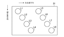
図3は、図2に示す露光装置20内の面発光レーザ31の発光面を示す図である。面発光レーザ31の発光面には、光源としての8個のレーザL1〜L8が格子状に2次元に配備されている。レーザL1,L5は、それぞれ副走査方向において同位置、すなわち同一の主走査ライン上に配備されている。同様に、レーザL2,L6、レーザL3,L7、レーザL4,L8も、それぞれ、副走査方向において同位置(同一の主走査ライン上)に配備されている。
FIG. 3 is a view showing a light emitting surface of the
また、レーザL1〜L4は、副走査方向の間隔が1画素となるように配列されている。同様に、レーザL5〜L8は、副走査方向の間隔が1画素となるように配列されている。さらに、レーザL1〜L4は、主走査方向の間隔が約2/3画素となるように配列されている。同様に、レーザL5〜L8は、主走査方向の間隔が約2/3画素となるように配列されている。また、後述する多重露光を行なうレーザL1,L5、レーザL2,L6、レーザL3,L7、及びレーザL4,L8は、それぞれ、約3.3画素分だけ離れて配設されている。 The lasers L1 to L4 are arranged so that the interval in the sub-scanning direction is one pixel. Similarly, the lasers L5 to L8 are arranged so that the interval in the sub-scanning direction is one pixel. Further, the lasers L1 to L4 are arranged so that the interval in the main scanning direction is about 2/3 pixels. Similarly, the lasers L5 to L8 are arranged so that the interval in the main scanning direction is about 2/3 pixels. Further, lasers L1 and L5, lasers L2 and L6, lasers L3 and L7, and lasers L4 and L8, which will be described later, are arranged apart from each other by about 3.3 pixels.
また、8個のレーザL1〜L8の仕様・性能は、同一の規格となっており、例えば、発振波長は約700〜800nmに統一されている。 Further, the specifications and performance of the eight lasers L1 to L8 are the same standard, and for example, the oscillation wavelength is unified to about 700 to 800 nm.
8個のレーザL1〜L8は、それぞれ、レーザドライバ16が備えるレーザ駆動回路LD1〜LD8を個別に有している。これらレーザ駆動回路LD1〜LD8は、レーザ制御部41の制御の下に、対応するレーザL1〜L8をON/OFF(選択)し、またその発光強度を切替え可能である。レーザ制御部41は、画像処理部40からの画像データ(ラスタライズ信号)に基づいて、面発光レーザ31によるレーザ発光を制御する。画像処理部40は、画像データに対する各種の補正処理等を行うと共に、ベクタ情報としての画像データをラスタライズしてビットマップ情報に変換する。
The eight lasers L1 to L8 individually have laser drive circuits LD1 to LD8 included in the
レーザ制御部41は、画像処理部40によりラスタライズされた1画素の画像データに基づいて、面発光レーザ31の8個のレーザL1〜L8を駆動制御する。換言すれば、レーザ制御部41は、ラスタライズされた1画素の画像データに基づくレーザL1〜L8の発光パターン(1画素内での走査開始起点)を、画像の属性データ(色、文字/非文字等)、濃度データ等の情報に基づいて決定する。
The
なお、以下の説明において、レーザL1〜L8を区別せずに一般的に説明する場合は、レーザLと称する。また、これらレーザL1〜L8を駆動するPWM信号についても、レーザL1〜L8と対応付けて区別する場合は、PWM信号S1〜S8と称し、区別せずに一般的に説明する場合は、PWM信号Sと称する。 In the following description, when the lasers L1 to L8 are generally described without being distinguished, they are referred to as lasers L. The PWM signals for driving the lasers L1 to L8 are also referred to as PWM signals S1 to S8 when distinguished from the lasers L1 to L8, and are generally described without distinction. Called S.
露光装置20は、レーザL1,L5(第1の光ビーム、第2の光ビーム)が同一画素を多重露光するように面発光レーザ31を駆動制御する。同様に、露光装置20は、レーザL2,L6、レーザL3,L7、及びレーザL4,L8が、それぞれ同一画素を多重露光するように面発光レーザ31を駆動制御する。なお、「同一画素」とは、画像データにおける同一のデータ成分を示すと同時に、感光体(感光ドラム25)上の同一の位置成分を示す用語である。また、本実施の形態における画像解像度は、主走査・副走査ともに600dpiである。
The
面発光レーザ31のレーザL1〜L8は、図4に示したPWM回路400により、個別に駆動される。すなわち、本実施の形態では、PWM回路400を、8個のレーザL1〜L8に対応して8個有している。換言すれば、多重露光に係る複数の光ビームは、複数の光源から個別に生成される。
Lasers L1 to L8 of the
図4のPWM回路400には、画像処理部40から濃度データとしての画像データ1と画像の属性データとしての画像識別データ7が入力される。画像データ1は、8bitのデータであり、16段階の濃度をしている。なお、この画像データ1は、ガンマ補正等の所定の画像処理が施されたものである。
The
画像データ1は、画像データ変換部2の変換テーブル3により、画像データ変換信号4に変換されて、D/Aコンバータ5に入力される。この画像データ変換信号4は、PWM信号Sのパルス幅(PWM信号Sの値が後述の「H」となるの期間)を決定する信号として機能する。D/Aコンバータ5は、デジタルの画像データ変換信号4をアナログ信号に変換する。その後、そのアナログの画像データ変換信号6の値をボリューム回路13で調整したD/A出力信号6aをコンパレータ12に出力する。
The
画像識別データ7は、2bitのデータであり、当該PWM回路400に現在入力されている画像データ1が、2値画像(ライン画像、例えば、文字画像)、階調画像(例えば、非文字画像)の何れの種類の画像データであるかを示している。この画像識別データ7は、後述する3つの参照波(中)9M、参照波(左)9L、参照波(右)9Rの中からいずれか1つを選択するための信号として利用される。つまり、画像識別データ7は、参照波(中)9Mは中央成長、参照波(左)9Lは左成長、参照波(右)9Rは右成長として、PWM信号の成長位置をいずれか1つを選択するための信号として利用される。
The
すなわち、画像識別データ7は、参照波供給部8のセレクタ10に入力される。参照波供給部8は、3つの参照波(中)9M、参照波(左)9L、参照波(右)9Rを生成する生成回路10M,10L,10Rを有している。これら参照波(中)9M、参照波(左)9L、参照波(右)9Rは、セレクタ10に入力される。セレクタ10は、画像識別データ7に基づいて、3つの参照波(中)9M、参照波(左)9L、参照波(右)9Rの中からいずれか1つを選択し、選択された参照波をコンパレータ12に出力する。
That is, the
コンパレータ12は、ボリューム回路13から出力されたD/A出力信号6aと、セレクタ10から出力された選択に係る参照波11とを比較する。そして、コンパレータ12は、D/A出力信号6aの方が参照波11より大きい間は「H」となり、それ以外の間は「L」となるPWM信号Sを、レーザドライバ16に出力する。
The
レーザドライバ16は、入力されたPWM信号Sに基づいて、対応するレーザLを駆動する。すなわち、レーザドライバ16は、PWM信号Sが「H」の期間はオン(発光)し、「L」の期間はオフ(消灯)するように、対応するレーザLを駆動制御する。なお、図4では、便宜上、全てのPWM信号S1,…,S8と、全てのレーザL1,…,L8を示しているが上述したように、レーザL1〜L8の夫々に対応する8個のPWM回路400が実際には存在する。また、以下の説明においても、この8個のPWM回路400はレーザL1〜L8と対応付けて区別することなく、PWM回路400と称する。
The
オフセット生成回路14は、選択された参照波11にオフセット成分を持たせる回路であり、そのオフセット量は、ボリューム回路15で調整することができる。本実施の形態では、このオフセット調整によって、画像データの値が「00h」の場合のPWM信号のパルス幅、すなわちPWM信号Sの最小のパルス幅の調整を可能にしている(00h調整)。
The offset
また、D/A変換回路5の出力をボリューム回路13で調整したD/A出力信号6aをコンパレータ12に入力することにより、画像データの値が「FFh」の場合のPWM信号の幅、すなわちPWM信号Sの最大のパルス幅の調整を可能にしている(FFh調整)。
Further, by inputting the D /
上記の00h調整とFFh調整により、PWM信号の幅は、画像データとレーザ光量の関係が線形になる領域、図12の例では「30h」〜「B0h」の領域で変化することとなる。 By the 00h adjustment and the FFh adjustment described above, the width of the PWM signal changes in a region where the relationship between the image data and the laser light amount is linear, in the region of “30h” to “B0h” in the example of FIG.
なお、PDセンサ36(図2)からの信号に基づいてタイミング信号17が生成され、PWM回路400には、このタイミング信号17が入力されている。PWM回路400は、このタイミング信号17に基づいて、感光ドラム25上の画像データに対応した所望の位置に静電潜像が形成されるように、対応のレーザLを駆動制御する。
A
すなわち、多重露光を行なうレーザL1,L5、レーザL2,L6、レーザL3,L7、及びレーザL4,L8は、前述のように、約3.3画素分だけ離れて配設されている。一方、レーザL1,L5からの光ビームは、ポリゴンミラー33の回転により偏向ビームとして感光ドラム25に照射される。従って、レーザL1,L5に係るPWM回路400には、画像データ1、タイミング信号17、後述する参照波等は、約3.3画素分だけタイミングをずらして供給される。これにより、感光ドラム25の同一点(同一の画素位置)を、レーザL1,L5からの同一画像データの同一画素に係る光ビームで多重露光することができる。
That is, the lasers L1 and L5, the lasers L2 and L6, the lasers L3 and L7, and the lasers L4 and L8 that perform multiple exposure are arranged apart from each other by about 3.3 pixels as described above. On the other hand, the light beams from the lasers L1 and L5 are applied to the
ただし、後述する図5,6,7,8のタイムチャートは、説明の便宜上、レーザL1,L5に関して、時間軸は同一の画素を基準として揃えられている。レーザL2,L6、レーザL3,L7、及びレーザL4,L8により多重露光を行なう場合も同様である。 However, in the time charts of FIGS. 5, 6, 7, and 8 to be described later, the time axes of the lasers L1 and L5 are aligned with reference to the same pixel for convenience of explanation. The same applies when multiple exposure is performed by the lasers L2 and L6, the lasers L3 and L7, and the lasers L4 and L8.
本実施の形態では、2値画像を形成する場合は、図5に示したように、多重露光を行なう2つのレーザLが、互いに異なる参照波を参照してPWM信号Sを生成する。つまり2つのレーザLが、互いに異なる走査開始起点となるように制御されている。図5は、レーザL1,L5により、主走査方向に600dpiのライン画像(2値画像)を形成する場合の参照波の波形とパルス幅変調信号(PWM信号)の波形、および得られたライン画像の形状を示している。なお、ここでは、レーザL1,L5により多重露光を行なう場合を説明するが、面発光レーザ31の発光面において同一の主走査ライン上に配備される二つのレーザを用いて多重露光を行うのであれば、これに限定されるものではない。例えば、レーザL2,L6、レーザL3,L7、及びレーザL4,L8により多重露光を行ってもよい。
In the present embodiment, when a binary image is formed, as shown in FIG. 5, the two lasers L that perform multiple exposure generate the PWM signal S with reference to different reference waves. That is, the two lasers L are controlled so as to have different scanning start points. FIG. 5 shows waveforms of a reference wave and a pulse width modulation signal (PWM signal) when a 600 dpi line image (binary image) is formed in the main scanning direction by the lasers L1 and L5, and the obtained line image. The shape is shown. Here, a case where multiple exposure is performed using the lasers L1 and L5 will be described. However, multiple exposure may be performed using two lasers arranged on the same main scanning line on the light emitting surface of the
レーザL1に対応するPWM回路400のセレクタ10は、画像識別データ7としてライン画像を示すデータが入力されると、参照波(右)9Rを選択する。また、ライン画像を形成する場合、画像データ1としては全画素について「FFh」がレーザL1に対応するPWM回路400に入力される。しかし、前述のように、D/A出力信号6aはボリューム回路13で調整されている。このため、図5に示したように、画像データ1の値「FFh」に対応するD/A出力信号6aの電位としては、参照波(右)9Rの最大電位よりも小さな値が設定される。
The
このため、画像データ1の値が「FFh」であっても、1画素の期間に対してレーザLが100%の期間点灯するわけではない。例えば、レーザL1に対応するPWM回路400のコンパレータ12から出力されるPWM信号S1は、図5に示すように、1画素の期間に対してレーザL1が80%の期間点灯することを示している。つまり、画素の右端を起点とした右成長で、幅が1画素の80%の幅のPWM信号を出力する。
For this reason, even if the value of the
レーザL5は、レーザL1によって露光された画素に対して多重露光を行なう。このレーザL5に対応するPWM回路400のセレクタ10は、画像識別データ7としてライン画像を示すデータが入力されると、参照波(左)9Lを選択する。画像データ1の値としては、レーザL5に対応するPWM回路400にもレーザL1に対応するPWM回路400と同様に、「FFh」が入力される。また、レーザL5に対応するPWM回路400から出力されるPWM信号S5は、図5に示すようになる。つまり、前述のように、D/A出力信号6aはボリューム回路13で調整されている。このため、図5に示したように、画像データ1の値「FFh」に対応するD/A出力信号6aの電位としては、参照波(左)9Lの最大電位よりも小さな値が設定される。このため、画像データ1の値が「FFh」であっても、1画素の期間に対してレーザLが100%の期間点灯するわけではない。つまり、レーザL5に対応するPWM回路400のコンパレータ12から出力されるPWM信号S1は、図5に示すように、1画素の期間に対してレーザL5が80%の期間点灯することを示している。つまり、画素の左端を起点とした左成長で、幅が1画素の80%の幅のPWM信号を出力する。
The laser L5 performs multiple exposure on the pixels exposed by the laser L1. When the data indicating the line image is input as the
ここで、レーザL1,L5に係るPWM回路400では、参照波としては、互いに対称関係にある鋸歯波形のものを使用している。換言すれば、レーザL1,L5に係るPWM回路400では、互いに位相を反転した状態の参照波を使用している。従って、レーザL1,L5に係るPWM回路400は、各画素の期間において互いに位相を反転させた形で「L」の部分(消灯期間)が出現するPWM信号S1,S5を出力する。具体的には、PWM信号S1は、各画素の期間(領域)のうちの最初の部分が消灯期間となり、PWM信号S5は、各画素の期間(領域)のうちの最後の部分が消灯期間となる。つまりレーザL1,L5は、互いに異なる走査開始起点となるように制御されている。
Here, in the
従って、レーザL1,L5により同一画素を多重露光してライン画像を形成する場合、多重露光される1の画素に着目すると、レーザL1,L5各々の露光位置がずれる為、1画素の期間中にレーザ光がオフ(無露光:消灯)となることは無い。つまり、1画素の全期間に亘って少なくともレーザL1,L5の一方がオン(露光:点灯)されている。このため、形成された画像においては、レーザL1で形成される画素とレーザL5で形成される画素各々の画素間でライン幅の細りが若干生じるものの、多重露光される画素ではラインが途切れることはなく、連続したラインとなる。換言すれば、ライン画像や文字画像の画質の低下を招くことなく、PWM信号Sに係る複数のレーザ光で多重露光を行うことが可能となる。 Therefore, when a line image is formed by multiple exposure of the same pixel with the lasers L1 and L5, focusing on one pixel that is subjected to multiple exposure, the exposure position of each of the lasers L1 and L5 is shifted. The laser light is never turned off (no exposure: extinguished). That is, at least one of the lasers L1 and L5 is turned on (exposure: lighting) over the entire period of one pixel. For this reason, in the formed image, although the line width is slightly narrowed between the pixels formed by the laser L1 and the pixels formed by the laser L5, the line is not interrupted in the multiple exposure pixels. There is no continuous line. In other words, it is possible to perform multiple exposure with a plurality of laser beams related to the PWM signal S without degrading the image quality of the line image or character image.
図6は、図5に対する比較例における2値画像の場合の各種信号波形と出力画像の形状を示す図である。すなわち、多重露光を行なうレーザL1,L5に係るPWM回路400では、共に参照波(右)9Rを使用するものと仮定する。この場合、多重露光を行なうレーザL1,L5に係るPWM回路400では、同一波形の参照波(右)9Rが使用され、かつこれら参照波(右)9Rは、同期した画素位置の波形データとしてコンパレータ12に供給される。
FIG. 6 is a diagram showing various signal waveforms and the shape of an output image in the case of a binary image in the comparative example with respect to FIG. That is, it is assumed that both the
従って、多重露光を行なうレーザL1,L5は、同一波形かつ同位相のPWM信号S1,S5で駆動制御され、多重露光される画素に着目すると、レーザL1,L5各々の露光位置が同じ為、多重露光される画素では、1画素の期間中で無露光の部分が生じる。このため、形成された画像においても、図6に示すように、途切れが有って画質が悪い2値画像(ライン画像、文字画像)となる。 Accordingly, the lasers L1 and L5 that perform multiple exposure are driven and controlled by the PWM signals S1 and S5 having the same waveform and the same phase, and focusing on the pixels that are subjected to multiple exposure, the exposure positions of the lasers L1 and L5 are the same. In the pixel to be exposed, an unexposed portion is generated in the period of one pixel. For this reason, even in the formed image, as shown in FIG. 6, a binary image (a line image or a character image) having a discontinuity and poor image quality is obtained.
一方、階調画像を形成する場合は、図7に示したように、レーザL1,L5により、同一画素内の同一位置を多重露光するようにする。なお、図7は、D/A出力信号6aの電位が画像データ1の値「30h」に対応する場合を示している。
On the other hand, when forming a gradation image, multiple exposure is performed on the same position in the same pixel by lasers L1 and L5 as shown in FIG. FIG. 7 shows a case where the potential of the D /
図7において、多重露光を行なうレーザL1,L5に係るPWM回路400のセレクタ10は、階調画像(例えば、非文字画像)を示す画像識別データ7により、同一の参照波を選択する。ここでは、共に参照波(右)9Rを選択している。また、これら参照波(右)9Rは、各画素について同期している。従って、レーザL1,L5に係るPWM回路400から出力されるPWM信号S1,S5は、パルス波形も位相も全く同様の信号となる。これにより、レーザL1,L5により、同一画素内の同一位置が多重露光され、形成された画像は、元の画像データが示す濃度を忠実に反映したものとなる。つまりレーザL1,L5が、互いに同一の走査開始起点となるように制御している。
In FIG. 7, the
これは、階調画像では、形成される画像の形状よりも濃度を表現するドットとしての面積の安定性の方がより重視されるからである。また、電子写真方式において電位ムラその他の外乱に対してドットを安定化するためには、静電潜像の電位を深くとることが好ましい。従って、階調画像の場合は、上記のように同一位置に多重露光する方がより良好な画像となる。 This is because in a gradation image, the area stability as a dot expressing density is more important than the shape of the formed image. Further, in order to stabilize the dots against potential unevenness and other disturbances in the electrophotographic system, it is preferable to take a deep potential of the electrostatic latent image. Therefore, in the case of a gradation image, it is better to perform multiple exposure at the same position as described above.
さらに、画像データに対する画像濃度の連続性を保つためにも、同一位置に多重露光するのが好ましい。これは1画素あたりに露光する総光量が同じでも、露光する領域の大きさによって濃度が変わってくるという、電子写真特有の特性によるものである。また、濃度の階調に対して、或る階調値で多重露光の照射位置を変えると、濃度変化の連続性が途切れる可能性がある。この点からも、階調画像では同一位置に多重露光する方がよい。 Further, in order to maintain continuity of image density with respect to image data, it is preferable to perform multiple exposure at the same position. This is due to the characteristic of electrophotography that the density varies depending on the size of the area to be exposed even if the total amount of light to be exposed per pixel is the same. Further, if the irradiation position of multiple exposure is changed with a certain gradation value with respect to the gradation of density, the continuity of density change may be interrupted. From this point, it is better to perform multiple exposure at the same position in the gradation image.
一方、文字画像やライン画像等の2値画像を形成する場合は、通常、最大光量で画像形成を行なうので濃度は安定しており、濃度よりも形状の正確性や解像度が重視される。従って、本実施の形態では、2値画像を形成する場合は、形状の正確性を重視し、連続してラインが形成されるようにしている。すなわち、本実施の形態では、画像データに対するレーザ光量のリニアリティを実現しながら、文字画像やライン画像において、途切れの無い良好な画像を形成できるようにしている。 On the other hand, when a binary image such as a character image or a line image is formed, since the image is normally formed with the maximum light quantity, the density is stable, and shape accuracy and resolution are more important than density. Therefore, in this embodiment, when forming a binary image, the accuracy of the shape is emphasized, and lines are continuously formed. That is, in the present embodiment, a good image without interruption is formed in a character image or a line image while realizing the linearity of the laser light quantity with respect to the image data.
本実施の形態を適用する場合、多重露光だけでなく単一露光でもライン画像、文字画像を形成できるように、各レーザL1〜L8の最大光量を設定しておくのが望ましい。これは、単一露光でライン画像、文字画像を形成できない場合、濃度の関係で画質が反って低下する場合も有り得るからである。 When this embodiment is applied, it is desirable to set the maximum light amounts of the lasers L1 to L8 so that a line image and a character image can be formed not only by multiple exposure but also by single exposure. This is because, when a line image and a character image cannot be formed by a single exposure, the image quality may be lowered due to the density.
なお、参照波の切替えは、画像データの画素ごとに行なうことも可能である。例えば、図8に示すように、各種の参照波の組み合わせ態様を画素ごとに適宜変化させて画像形成を行なうことも可能である。つまり、上記では、画像識別データ7に応じて、主走査方向の1ライン単位で参照波(中)9M、参照波(左)9L、及び参照波(右)9Rを選択した。しかし、かかる画像形成に限定されるものでない。例えば、主走査方向に文字部と非文字部、つまり二値画像と階調画像とが併設されている場合、1ラインの途中で画像識別データ7に応じて、参照波(中)9M、参照波(左)9L、及び参照波(右)9Rを切り替えるようにしても良い。さらに、画素単位で、参照波(中)9M、参照波(左)9L、及び参照波(右)9Rを選択するようにしてもよい。図8は、1、2画素目で参照波(右)9Rを選択し、3画素目で参照波(中)9Mを選択し、4画素目で参照波(左)9Lを選択し、5画素目で参照波(右)9Rを選択した場合の例である。つまり画像識別データ7に応じて、隣接する画素毎に互いに異なる走査開始起点となるように制御してもよく、多重露光を行う際のレーザL各々で異なる走査開始起点となるように制御してもよい。
It should be noted that the reference wave can be switched for each pixel of the image data. For example, as shown in FIG. 8, it is also possible to form an image by appropriately changing the combination of various reference waves for each pixel. That is, in the above description, the reference wave (middle) 9M, the reference wave (left) 9L, and the reference wave (right) 9R are selected in units of one line in the main scanning direction according to the
本発明は、上記の実施の形態に限定されることなく、例えば、図9のように構成された面発光レーザ31を用いることも可能である。
The present invention is not limited to the above embodiment, and for example, a
図3に示した面発光レーザ31では、同一の主走査ライン上に形成され、副走査方向に離間していない2つのレーザL1,L5、レーザL2,L6、レーザL3,L7、及びレーザL4,L8により、それぞれ多重露光を行なっていた。これに対し、図9に示した面発光レーザ31では、異なる主走査ライン上に配備され、副走査方向に離間している2つのレーザL1,L5、レーザL2,L6、レーザL3,L7、及びレーザL4,L8により、それぞれ多重露光が行なわれる。
In the
すなわち、図9に示した面発光レーザ31は、レーザL1〜L8は副走査方向に1画素間隔で配列され、主走査方向に2/3画素間隔で配列されている。そして、像担持体上を露光走査する際には、レーザL1〜L4による露光走査は、前回の露光走査でレーザL5〜L8が露光走査した主走査ラインに重複させて行う。
That is, in the
換言すれば、レーザL1,L5、レーザL2,L6、レーザL3,L7、及びレーザL4,L8には、前回と今回の露光走査とで、それぞれ同一の主走査ラインに係る画像データに基づくPWM信号が供給されて、同一の画素が多重露光されることとなる。この露光走査方法は、画像形成スピードの面ではこの実施例の場合では半分の速度になる為、不利であるが、走査間隔のバラツキによるスジ画像が目立たなくなるという利点がある。なお、参照波の選択方法等は、図3の面発光レーザ31の場合と同様であるので、その詳細な説明は省略する。
In other words, the laser signals L1 and L5, the lasers L2 and L6, the lasers L3 and L7, and the lasers L4 and L8 are PWM signals based on image data related to the same main scanning line in the previous exposure scan and the current exposure scan, respectively. Is supplied, and the same pixel is subjected to multiple exposure. This exposure scanning method is disadvantageous in terms of image forming speed because it is half the speed in the case of this embodiment, but has the advantage that streak images due to variations in scanning intervals are not noticeable. The reference wave selection method and the like are the same as in the case of the
また、PWM回路400は、図4のように、参照波を用いる回路ではなく、例えば1画素走査時間よりも十分高い周波数のクロック周波数で駆動するデジタルのPWM回路としてもよい。これにより、多重露光に係る光ビームの無露光部が重ならないように任意の位相でPWM信号を形成することも可能である。
Further, the
また、上記の実施の形態では、2値画像を形成する場合に、多重露光に係る光ビーム間で各画素における発光タイミングを異ならせ、階調画像を形成する場合には、各画素における発光タイミングを同一にしていた。これに対し、例えば薄い濃度のライン画像など、画像データの値が一定の範囲にあり、濃度の安定より形状を優先する任意の画像において、多重露光に係る光ビーム間で各画素における発光タイミングを異ならせるようにしてもよい。 In the above embodiment, when a binary image is formed, the light emission timing in each pixel is made different between the light beams related to multiple exposure, and in the case of forming a gradation image, the light emission timing in each pixel. Were the same. In contrast, in an arbitrary image in which the value of the image data is in a certain range, such as a line image with a low density, and the shape is prioritized over the stability of the density, the light emission timing in each pixel is set between the light beams related to multiple exposure. You may make it differ.
さらに、3つ以上の光ビームを用いて同一画素位置を多重露光する場合にも、上記の実施の形態を適用し、2値画像等を形成する場合に無露光の画素領域を無くすことも可能である。 Furthermore, even when multiple exposures are performed on the same pixel position using three or more light beams, the above-described embodiment can be applied to eliminate a non-exposed pixel region when forming a binary image or the like. It is.
8 参照波供給部
10 セレクタ
12 コンパレータ
20 露光装置
25 感光ドラム
31 面発光レーザ
L1〜L8 レーザ
8 Reference
Claims (2)
複数の光ビームを射出する光源と、
前記光源から射出された前記複数の光ビームが前記感光体上を走査するように前記複数の光ビームを偏向する偏向手段と、
文字画像を形成する場合、前記感光体上において各画素に対応する画像データに基づいて行われる第1露光の露光領域と第2露光の露光領域とが前記感光体上を走査する光ビームの走査方向において相対的にずれるように前記光源からの前記光ビームの出射タイミングを制御し、階調画像を形成する場合、前記感光体上において各画素に対応する画像データに基づいて行われる第1露光の露光領域と第2露光の露光領域とが前記走査方向において同一位置になるように前記光源からの前記光ビームの出射タイミングを制御する制御手段とを備えることを特徴とする画像形成装置。 In an image forming apparatus for forming an electrostatic latent image by multiple exposure of the same pixel position on a photoconductor based on image data,
A light source that emits a plurality of light beams;
A deflection means for the plurality of light beams emitted from the light source to deflect the plurality of light beams to scan over the photosensitive member,
When a character image is formed, a light beam is scanned on the photoconductor by the exposure area of the first exposure and the exposure area of the second exposure performed on the photoconductor based on image data corresponding to each pixel. When the gradation timing image is formed by controlling the emission timing of the light beam from the light source so as to be relatively shifted in the direction, the first exposure is performed based on image data corresponding to each pixel on the photoreceptor. An image forming apparatus comprising: a control unit configured to control the emission timing of the light beam from the light source so that the exposure area of the second exposure area and the exposure area of the second exposure are in the same position in the scanning direction.
Priority Applications (2)
| Application Number | Priority Date | Filing Date | Title |
|---|---|---|---|
| JP2008194345A JP5274139B2 (en) | 2007-08-02 | 2008-07-29 | Image forming apparatus |
| US12/184,498 US8213049B2 (en) | 2007-08-02 | 2008-08-01 | Image forming apparatus |
Applications Claiming Priority (3)
| Application Number | Priority Date | Filing Date | Title |
|---|---|---|---|
| JP2007201947 | 2007-08-02 | ||
| JP2007201947 | 2007-08-02 | ||
| JP2008194345A JP5274139B2 (en) | 2007-08-02 | 2008-07-29 | Image forming apparatus |
Publications (3)
| Publication Number | Publication Date |
|---|---|
| JP2009051206A JP2009051206A (en) | 2009-03-12 |
| JP2009051206A5 JP2009051206A5 (en) | 2011-09-15 |
| JP5274139B2 true JP5274139B2 (en) | 2013-08-28 |
Family
ID=40502713
Family Applications (1)
| Application Number | Title | Priority Date | Filing Date |
|---|---|---|---|
| JP2008194345A Expired - Fee Related JP5274139B2 (en) | 2007-08-02 | 2008-07-29 | Image forming apparatus |
Country Status (1)
| Country | Link |
|---|---|
| JP (1) | JP5274139B2 (en) |
Families Citing this family (2)
| Publication number | Priority date | Publication date | Assignee | Title |
|---|---|---|---|---|
| JP2011237384A (en) * | 2010-05-13 | 2011-11-24 | Hitachi High-Technologies Corp | Optical system for analysis and analyzer using the same |
| JP2016021664A (en) * | 2014-07-14 | 2016-02-04 | 株式会社リコー | Image forming apparatus |
Family Cites Families (8)
| Publication number | Priority date | Publication date | Assignee | Title |
|---|---|---|---|---|
| JP2642406B2 (en) * | 1988-05-19 | 1997-08-20 | 株式会社リコー | Image forming device |
| JP3165922B2 (en) * | 1990-07-16 | 2001-05-14 | コニカ株式会社 | Image forming device |
| JP2657430B2 (en) * | 1991-01-30 | 1997-09-24 | 東燃株式会社 | Polyolefin microporous membrane and method for producing the same |
| JP3333964B2 (en) * | 1992-01-07 | 2002-10-15 | コニカ株式会社 | Image forming method |
| JPH05130347A (en) * | 1991-11-01 | 1993-05-25 | Konica Corp | Image forming device |
| JPH09218568A (en) * | 1996-02-14 | 1997-08-19 | Fuji Xerox Co Ltd | Image forming device |
| JP2002002022A (en) * | 2000-06-26 | 2002-01-08 | Canon Inc | Apparatus and method for imaging |
| JP2005161657A (en) * | 2003-12-02 | 2005-06-23 | Canon Inc | Image forming device |
-
2008
- 2008-07-29 JP JP2008194345A patent/JP5274139B2/en not_active Expired - Fee Related
Also Published As
| Publication number | Publication date |
|---|---|
| JP2009051206A (en) | 2009-03-12 |
Similar Documents
| Publication | Publication Date | Title |
|---|---|---|
| US9527303B2 (en) | Image forming apparatus and image forming method to form an image by scanning an image bearer with light modulated based on image information | |
| JP6484059B2 (en) | Image forming apparatus and image forming method | |
| JP6489861B2 (en) | Image forming apparatus | |
| US5144337A (en) | Image forming apparatus capable of forming an image by dots having various diameters | |
| US9091956B2 (en) | Image forming apparatus for performing exposure a plurality of times | |
| JPH066536A (en) | Image forming device | |
| JP3245205B2 (en) | Image forming device | |
| JP5274139B2 (en) | Image forming apparatus | |
| US8213049B2 (en) | Image forming apparatus | |
| JP2000190554A (en) | Optical scanning apparatus | |
| JP4926587B2 (en) | Semiconductor laser drive control device | |
| JP7019365B2 (en) | Image forming device | |
| JP2017056673A (en) | Image forming apparatus, image forming method, and program | |
| JP4541910B2 (en) | Image forming apparatus | |
| JP6700744B2 (en) | Image forming apparatus and control method thereof | |
| US7408567B2 (en) | Light beam scanning apparatus and image forming apparatus | |
| JP3705337B2 (en) | Thin line scanning recording method | |
| JP3563776B2 (en) | Image forming apparatus and method | |
| JPH01206368A (en) | Image forming device | |
| JP6536361B2 (en) | Image forming apparatus and image forming control method | |
| JP2009034994A (en) | Image forming apparatus and control method therefor | |
| JP3012311B2 (en) | Color image forming equipment | |
| JPH11216908A (en) | Image-forming apparatus | |
| JP2020021010A (en) | Image formation device | |
| JP2003154705A (en) | Imaging apparatus |
Legal Events
| Date | Code | Title | Description |
|---|---|---|---|
| A521 | Written amendment |
Free format text: JAPANESE INTERMEDIATE CODE: A523 Effective date: 20110722 |
|
| A621 | Written request for application examination |
Free format text: JAPANESE INTERMEDIATE CODE: A621 Effective date: 20110722 |
|
| A521 | Written amendment |
Free format text: JAPANESE INTERMEDIATE CODE: A523 Effective date: 20110725 |
|
| A131 | Notification of reasons for refusal |
Free format text: JAPANESE INTERMEDIATE CODE: A131 Effective date: 20121106 |
|
| A521 | Written amendment |
Free format text: JAPANESE INTERMEDIATE CODE: A523 Effective date: 20130107 |
|
| A131 | Notification of reasons for refusal |
Free format text: JAPANESE INTERMEDIATE CODE: A131 Effective date: 20130129 |
|
| A521 | Written amendment |
Free format text: JAPANESE INTERMEDIATE CODE: A523 Effective date: 20130328 |
|
| TRDD | Decision of grant or rejection written | ||
| A01 | Written decision to grant a patent or to grant a registration (utility model) |
Free format text: JAPANESE INTERMEDIATE CODE: A01 Effective date: 20130416 |
|
| A61 | First payment of annual fees (during grant procedure) |
Free format text: JAPANESE INTERMEDIATE CODE: A61 Effective date: 20130514 |
|
| LAPS | Cancellation because of no payment of annual fees |