JP5259706B2 - Method and apparatus for searching for location of network failure - Google Patents
Method and apparatus for searching for location of network failure Download PDFInfo
- Publication number
- JP5259706B2 JP5259706B2 JP2010513243A JP2010513243A JP5259706B2 JP 5259706 B2 JP5259706 B2 JP 5259706B2 JP 2010513243 A JP2010513243 A JP 2010513243A JP 2010513243 A JP2010513243 A JP 2010513243A JP 5259706 B2 JP5259706 B2 JP 5259706B2
- Authority
- JP
- Japan
- Prior art keywords
- signal
- network
- fault
- encoder
- probe
- Prior art date
- Legal status (The legal status is an assumption and is not a legal conclusion. Google has not performed a legal analysis and makes no representation as to the accuracy of the status listed.)
- Expired - Fee Related
Links
Images


Classifications
-
- H—ELECTRICITY
- H04—ELECTRIC COMMUNICATION TECHNIQUE
- H04N—PICTORIAL COMMUNICATION, e.g. TELEVISION
- H04N17/00—Diagnosis, testing or measuring for television systems or their details
Landscapes
- Engineering & Computer Science (AREA)
- Health & Medical Sciences (AREA)
- Biomedical Technology (AREA)
- General Health & Medical Sciences (AREA)
- Multimedia (AREA)
- Signal Processing (AREA)
- Arrangements For Transmission Of Measured Signals (AREA)
- Small-Scale Networks (AREA)
- Monitoring And Testing Of Transmission In General (AREA)
- Medicines Containing Material From Animals Or Micro-Organisms (AREA)
- Agricultural Chemicals And Associated Chemicals (AREA)
Abstract
Description
本出願は、2007年6月19日に提出の米国仮特許出願第60/945,094号の優先権の利益を主張する。 This application claims the benefit of priority of US Provisional Patent Application No. 60 / 945,094, filed Jun. 19, 2007.
本発明は、一般的にネットワーク監視システムに関し、更に詳しくは、ハイブリッド・ファイバー同軸(HFC)ネットワークにおける障害の位置を探索する方法および装置に関する。 The present invention relates generally to network monitoring systems, and more particularly to a method and apparatus for locating faults in a hybrid fiber coax (HFC) network.
2つのカテゴリーの障害が、一般的にHFCネットワーク内に存在する。それらは、(1)共通の経路歪み(CPD)、および、(2)雑音である。雑音源は、ネットワークの内部に、或いは、ネットワークの外部にあるかも知れない。後者は「侵入」と呼ばれる。HFCネットワーク中の上り回線帯域に関する、CPDおよび/または雑音による音声およびデータトラフィックの送信の難しさは、よく知られており、過去10〜15年間で十分に文書で示された。やがて、オペレーターは、それらネットワーク上のトラフィック量を増加させたいとする増大する要求を満たすために、ホームからの上り送信のために、高い処理能力のフォーマットへ移行させた(例えば16QAM)。これら高次の変調信号は、本質的に雑音と同様にCPDにより敏感である。エラー訂正および他のスキームがこの感度を最小化するために導入されてきたものの、その問題はまだ存在する。上り回線中の過度のCPDおよび雑音は、音声とデータのようなサービスに混乱をもたらす場合がある。そのため、そのようなネットワークのオペレーターには、その問題を回復し顧客の不通を最小化できるように、これら障害源の位置を素早く見つけることが重要であり且つ価値がある。 Two categories of failures are generally present in HFC networks. They are (1) common path distortion (CPD) and (2) noise. The noise source may be internal to the network or external to the network. The latter is called “intrusion”. The difficulty of transmitting voice and data traffic due to CPD and / or noise with respect to uplink bandwidth in HFC networks is well known and has been well documented in the past 10-15 years. Eventually, operators moved to higher throughput formats for upstream transmission from the home (eg, 16QAM) to meet the increasing demand to increase the amount of traffic on those networks. These higher order modulation signals are inherently more sensitive to CPD as well as noise. Although error correction and other schemes have been introduced to minimize this sensitivity, the problem still exists. Excessive CPD and noise in the uplink can cause disruption to services such as voice and data. Therefore, it is important and valuable for operators of such networks to quickly locate these fault sources so that they can recover from the problem and minimize customer disruption.
幾つかの方策が、問題が生じた際にそれを探索し解決するために使用される方法と共に、ネットワーク上で上り回線障害を管理しようとするオペレーターによって採用されている。 Several strategies have been adopted by operators seeking to manage uplink failures on the network, along with methods used to find and resolve problems as they arise.
オペレーターによっては、侵入を管理する目的で、加入者宅から来る侵入を減らす受動フィルタ(ハイパス・フィルタ、ウィンドウ・フィルタまたはステップ減衰フィルタ)のような装置を設置することを選択している。別の取り組みでは、トラフィックが使用されていない期間に上り回線信号の全てあるいは一部を減衰させ、トラフィックが存在しているときには、全ての信号を通過させる動的侵入阻止(DIB)システムを導入する。この後者の取り組みは、トラフィックが存在しないときには侵入を効果的に阻止し、且つ、トラフィックが存在するときにはトラフィックのネットワークへの進入を許す。これらの取組みが、完全には有効でないこと、および、騒音源および侵入源を探索し除去することを試みてはいないことに注意すべきである。多くのオペレーターは、それに代えて、如何なる雑音緩和装置をも使用しないことを選択している。 Some operators have chosen to install devices such as passive filters (high-pass filters, window filters or step-attenuation filters) that reduce intrusions coming from the subscriber's home for the purpose of managing intrusions. Another approach is to introduce a dynamic intrusion prevention (DIB) system that attenuates all or part of the uplink signals during periods when traffic is not in use, and allows all signals to pass when traffic is present. . This latter approach effectively prevents intrusion when there is no traffic and allows traffic to enter the network when there is traffic. It should be noted that these efforts are not completely effective and do not attempt to locate and remove noise and intrusion sources. Many operators have chosen not to use any noise mitigation device instead.
問題を見つけて解決するために、多くのオペレーターが上り回線スペクトル分析監視システムを導入した。雑音または侵入の問題がヘッドエンドで測定される場合、典型的なプロセスでは、専門家がフィールドに入り、上りシステムの一部を一時的に切り離し、その切離しがヘッドエンドで持つ効果を同時にモニターしつつ、直接的にトラブルシュートする。上り区間が引き抜かれているときに、侵入あるいは他の雑音がヘッドエンドで減少すれば、これが侵入または他の雑音が起こった方向だったという結論が得られる。雑音源または侵入源が見つかるまで、この試行錯誤プロセスは継続する。それは大きな時間消費であるかも知れない。 To find and solve the problem, many operators have installed an uplink spectrum analysis and monitoring system. When noise or intrusion problems are measured at the headend, a typical process involves an expert entering the field, temporarily disconnecting part of the upstream system, and simultaneously monitoring the effect that disconnection has on the headend. While directly troubleshooting. If the intrusion or other noise is reduced at the headend when the upswing is being drawn, the conclusion can be drawn that this was the direction in which the intrusion or other noise occurred. This trial and error process continues until a noise or intrusion source is found. It may be a big time consumption.
他に採用されているシステムには、アーコム・デジタル社からのHunterRシステムがあり、そのシステムは、2006年11月2日公開の特許文献1および2004年12月9日公開の特許文献2に記載されている。これら記載されたシステムは、下り回線信号から生成された模擬CPD信号を、上り回線から測定された信号と比較する受動検出技術および相関処理を用いる。これらのシステムは、相関処理から決定された時間遅れから起源への距離を計算することにより、HFCネットワーク中のCPD源の位置を正確に示すことができる。しかし、ケーブルテレビジョン業界で利用されるネットワーク地図に固有の不正確さにより、起源を探し出すには、更なる努力がしばしば必要である。これらの更なる努力は時間消費となり得る。 Other systems employed include the HunterR system from Arkcom Digital, which is described in US Pat. No. 5,099,028 published on Nov. 2, 2006 and U.S. Pat. Has been. These described systems use passive detection techniques and correlation processing that compares the simulated CPD signal generated from the downlink signal with the signal measured from the uplink. These systems can accurately indicate the position of the CPD source in the HFC network by calculating the distance from the time delay determined from the correlation process to the origin. However, due to the inaccuracies inherent in network maps used in the cable television industry, further efforts are often required to find the origin. These additional efforts can be time consuming.
障害がヘッドエンドで測定される場合、ネットワーク・オペレータは、その問題の原因を見つけようとして、様々な方法を使用することが出来る。HFCネットワーク上の典型的なノードでは、多くのブランチおよび何百もの装置があり、その各々がその問題の原因であるかも知れない。その問題の原因の位置を見つけることは、時間を消費する努力であるかも知れない。幾つかのケーブルシステムでは、そのシステムの様々な部分への侵入および他のノイズ信号を減衰させて、ユーザが雑音源および侵入源の位置を見付けるのを支援する、(「ウィンク」スイッチと呼ばれる)低減衰値スイッチを利用する。各ウィンク・スイッチは、固有のアドレスを持ち、ノード内の様々なスイッチは連続してアドレス指定され、スイッチが取り付けられたネットワーク区間の上り回線上に数dBの追加減衰が導入されるようにオンされる。このスイッチングが発生している間に、ヘッドエンドの上り回線スペクトルがモニターされ、それによって、スイッチがいつオンするかのタイミングが、ヘッドエンドでの対応する量の騒音レベル低下に相当するならば、特定の区間を指し示すことになる。別の技術は、起源をトラブルシュートする試みで、フィールド・スペクトラム・アナライザーを使用する。他のシステム・オペレータは、起源を三角測量しようとする試みで、システムの周りで運転されているトラックに設置されたダイポール・アンテナを使用する。その他のシステム・オペレータは、先に述べたハンターRシステムを使用するかも知れない。 If a failure is measured at the headend, the network operator can use various methods to try to find the cause of the problem. In a typical node on an HFC network, there are many branches and hundreds of devices, each of which may be responsible for the problem. Finding the location of the cause of the problem may be a time consuming effort. Some cable systems attenuate intrusion and other noise signals into various parts of the system to help the user locate the noise source and intrusion source (referred to as a “wink” switch) Use a low attenuation switch. Each wink switch has a unique address, and the various switches in the node are addressed consecutively and are turned on so that an additional attenuation of several dB is introduced on the uplink of the network section where the switch is attached. Is done. While this switching occurs, if the head end uplink spectrum is monitored, so that the timing of when the switch is turned on corresponds to a corresponding amount of noise level drop at the head end, It points to a specific section. Another technique uses field spectrum analyzers in an attempt to troubleshoot the origin. Other system operators use dipole antennas installed on trucks driving around the system in an attempt to triangulate their origin. Other system operators may use the Hunter R system described above.
上記で述べた方法には欠点がある。DIBまたはウィンク・スイッチの何れかによる取組みでは、装置のアドレス指定をするため上り回線上のデータを転送する追加の搬送波を導入することが必要になる。更に、フィールドに設置されたアドレス指定可能な装置は複雑であり、比較的高価でもある。DIBによる取組みでは、追加の装置をケーブルネットワークに設置することが必要になる。これは、システム休止時間およびサービス中断を必要とする、費用がかかる手順である。これら追加の装置は、更にネットワーク問題の潜在的な新しい原因にもなる。そのような装置の電力消費は、幾つかの適用ではそれらを使用不可能とするか、或いは、ネットワークへの再配置または追加の電源を必要とさせるかもしれない。ウィンク・スイッチの場合には、それらは能動装置にのみ設置されるので、そのようなスイッチの数はネットワーク中で制限されるかもしれない。最後に、ウィンク・スイッチの場合には、スイッチの減衰量(典型的には、3または6dB)が、ネットワークトラフィックに混乱を発生させる。 The method described above has drawbacks. Efforts by either DIB or wink switches require the introduction of an additional carrier to transfer data on the uplink to address the device. Furthermore, addressable devices installed in the field are complex and relatively expensive. The DIB approach requires that additional devices be installed in the cable network. This is an expensive procedure that requires system downtime and service interruption. These additional devices are also a potential new source of network problems. The power consumption of such devices may make them unusable in some applications, or may require relocation to the network or additional power sources. In the case of wink switches, the number of such switches may be limited in the network because they are installed only on active devices. Finally, in the case of a wink switch, the switch attenuation (typically 3 or 6 dB) causes disruption to the network traffic.
本明細書では、用語「エンコーダ」、「エンコーダ装置」、「IDエンコーダ」または「プローブ」は、適切な位置でケーブルネットワークに設置され、ネットワーク中の信号トラフィック上で、IDコード、例えば周波数分割IDまたは符号分割ID(以下で更に述べる)を付与するか、コード化する装置を指す。その結果、装置の位置、および、装置の下流側に起源を有する任意の障害の位置を決定することが出来る。その装置は、障害が由来するネットワークの区間またはブランチをマークするかフラグを立てるためにそれを設置することが出来るので、「マーカー」または「マーカー装置」とも呼ばれることがある。 As used herein, the terms “encoder”, “encoder device”, “ID encoder” or “probe” are installed in a cable network at an appropriate location, and on signal traffic in the network, an ID code, eg, frequency division ID Or a device that assigns or encodes a code division ID (discussed further below). As a result, the location of the device and the location of any faults originating from the downstream side of the device can be determined. The device may also be referred to as a “marker” or “marker device” because it can be set up to mark or flag a network segment or branch from which the fault originated.
本発明は、先行技術に関連した問題を克服する、HFCケーブルネットワーク内で障害の位置を探索する方法および装置を提供することを目的とする。 The present invention seeks to provide a method and apparatus for locating faults in an HFC cable network that overcomes the problems associated with the prior art.
本発明は、従来の方法および装置よりも、ネットワーク障害の位置をより正確に見つけ出す方法および装置を提供することを別の目的とする。 It is another object of the present invention to provide a method and apparatus for more accurately locating network failures than conventional methods and apparatus.
本発明は、上り回線周波数帯域内で追加信号の送信を必要としないで、ネットワーク障害の位置を探索する方法および装置を提供することを更に別の目的とする。 It is yet another object of the present invention to provide a method and apparatus for searching for the location of a network failure without requiring transmission of additional signals within the uplink frequency band.
本発明は、ネットワーク内でアドレス指定可能な装置の展開を必要としないで、ネットワーク障害の位置を探索する方法および装置を提供することを更に別の目的とする。 It is yet another object of the present invention to provide a method and apparatus for searching for the location of a network failure without requiring deployment of an addressable device within the network.
本発明は、設置するのが簡単で、その設置がネットワークの切断や加入者へのサービス中断を必要とすることなくネットワーク中に展開されるエンコーダまたはマーカー装置を有する、ネットワーク障害を見つける方法および装置を提供することを更に別の目的とする。 The present invention is a method and apparatus for finding network faults having encoder or marker devices that are simple to install and that are deployed in the network without requiring network disconnection or service interruption to subscribers It is yet another object to provide
本発明は、比較的単純な設計および低価格であるエンコーダまたはマーカー装置を有する、ネットワーク障害を見つける方法および装置を提供することを更に別の目的とする。 It is yet another object of the present invention to provide a method and apparatus for finding network faults having a relatively simple design and low cost encoder or marker device.
本発明は、ネットワークの下り回線または上り回線の何れかでサービスを中断または妨害することがないエンコーダまたはマーカー装置を有する、ネットワーク障害を見つける方法および装置を提供することを更に別の目的とする。 It is yet another object of the present invention to provide a method and apparatus for finding network failures having an encoder or marker device that does not interrupt or disrupt service on either the downlink or uplink of the network.
上記および他の目的は、FHCネットワーク内で障害の位置を探索する、本発明に係るシステムによって達成され、該システムは:(a)侵入またはCPDのような障害がネットワーク内に存在するかどうかを判定するネットワーク障害検出器;(b)既知の符号化地点に展開され、符号化地点の下流側で発生する(障害によって発生した信号を含む)上り回線信号をIDコードによって符号化する少なくとも1つのエンコーダまたはマーカー装置;IDコードを解読しエンコーダおよび符号化地点を特定するデコーダユニットを備え、前記障害検出器で検出される何れのネットワーク障害も前記符号化地点の下流側にあると判定する。
好ましい実施形態では、エンコーダまたはマーカー装置は、ネットワーク内に既に設置されている分配器、マルチタップ、増幅器またはその他のネットワーク受動装置または能動装置のアクセスポート(または押さえポート)にねじ込まれるねじ型プローブの形状を有する。プローブは、装置内の押さえねじと接触する。従って、好ましい設置方法では、ケーブルの切断やサービスの中断などを必要としない。好ましい符号化の方法は、上り信号の単一周波数、周期関数による振幅変調(AM)である。この場合、デコーダユニットは、振幅復調器である。好ましい実施形態では、デコーダユニットは、障害検出ユニットと組み合わされる。
The above and other objects are achieved by a system according to the present invention that locates a fault in an FHC network, which system: (a) determines whether a fault such as intrusion or CPD exists in the network. A network failure detector for determining; (b) at least one encoded with an ID code for an uplink signal (including a signal generated by the failure) that is developed downstream of the encoding point and is generated downstream of the encoding point An encoder or marker device; comprising a decoder unit that decodes the ID code and identifies the encoder and the encoding point, and determines that any network fault detected by the fault detector is downstream of the encoding point.
In a preferred embodiment, the encoder or marker device is a threaded probe that is screwed into the access port (or hold-down port) of a distributor, multi-tap, amplifier or other network passive or active device already installed in the network. Has a shape. The probe contacts a set screw in the device. Therefore, the preferred installation method does not require cable disconnection or service interruption. A preferred encoding method is amplitude modulation (AM) by a single frequency and periodic function of the upstream signal. In this case, the decoder unit is an amplitude demodulator. In a preferred embodiment, the decoder unit is combined with a fault detection unit.
本発明は、HFCネットワーク内で障害の位置を探索する方法も意図している。そのような1つの方法は:(a)下り回線および上り回線を有するネットワークの符号化地点にIDエンコーダを設置するステップ;(b)符号化地点よりも上流側のネットワークの少なくとも1つの地点に障害検出器およびIDデコーダを設置するステップ;(c)上り回線周波数帯域の少なくとも一部の信号であって前記符号化地点の下流側で発生する信号にエンコーダからのIDコードを付与するステップ;テスト地点で符号化された信号を受信するステップ;(e)ネットワーク障害検出器で、符号化された信号から障害が検出されたかどうかを判定するステップ;および、(f)IDデコーダでIDコードを復号してネットワーク中のIDエンコーダおよび符号化地点を特定するステップを有し、先のステップで検出された何れの障害も前記符号化地点の下流側であると判定する。 The present invention also contemplates a method for locating a fault within an HFC network. One such method is: (a) installing an ID encoder at a coding point of a network having a downlink and an uplink; (b) failure at at least one point in the network upstream from the coding point. Installing a detector and an ID decoder; (c) adding an ID code from the encoder to a signal that is at least a part of an uplink frequency band and is generated downstream of the encoding point; a test point; Receiving the signal encoded in (i); (e) determining whether a failure is detected from the encoded signal in the network failure detector; and (f) decoding the ID code in the ID decoder. To identify the ID encoder and encoding point in the network, and any of the detected in the previous step Harm determines that downstream of the coding point.
本発明の更なる目的は、添付の図面を参照する好ましい実施形態の以下の記述から明白になるであろう。 Further objects of the present invention will become apparent from the following description of preferred embodiments with reference to the accompanying drawings.
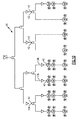
図1は、本発明の一実施形態に係る障害位置探索システムAのブロック図を示す。システムAは、CATVヘッドエンドB、および、HFCケーブルTVネットワークの同軸ケーブル部分10に組み入れられる。システムAは、ヘッドエンドで接続されている次の装置:ヘッドエンド障害検出および復号ユニット1、上り回線スイッチ3、および、コンピューター2を有する。システムAは、更にHFCネットワークの同軸ケーブル部分10に接続または統合された少なくとも1台のIDエンコーダ12を含んでいる。一般的なヘッドエンド装置は、下り回線信号(つまり、アナログおよびデジタルTVプログラム信号)を合成するヘッドエンド・コンバイナー4、複数の光学ノードに下り回線信号を配信する信号分配器5、HFCネットワークの光ファイバー部分内のファイバー光学ノードに下り回線信号を送信する複数の光送信器6、および、光学ノードから上り回線信号を受信し且つヘッドエンド・レシーバー(図示せず)にそれらを配信する複数の受光器7を備える。
ヘッドエンド障害検出および復号ユニット1は、2つの入力を有し、一方は上り回線スイッチ3の出力に接続され、他方はタップ11を介してコンバイナー4の出力に接続される。ユニット1の出力(「RF出力」)は、コンバイナー4の入力に接続される。下り回線のアナログおよびデジタルTVプログラム信号は、コンバイナー4の他の入力に印加される。コンバイナー4の合成出力は、分配器5の入力に接続される。分配器5の出力は、光送信器6の入力に接続される。図1に示されるように、下り回線信号は、光ケーブル上の送信器6から、対応する光学ノード8に送信される。以前に述べたように、コンバイナー4の出力は、タップ11を介してユニット1の入力(つまり「下り回線入力」)にも接続される。
FIG. 1 shows a block diagram of a fault location searching system A according to an embodiment of the present invention. System A is incorporated into CATV headend B and
The headend failure detection and
ユニット1およびスイッチ3の管理は、コンピューター2の支援を受けて行なわれる。図1に示されるように、コンピューター2は、ユニット1およびスイッチ3に接続される。コンピューター2は、スイッチ3を制御するようにプログラムされ、スイッチ3に、各受光器7からの上り回線信号をユニット1の別の入力(つまり、「上り回線入力」)に、個別に、且つ、周期的にまたはプログラムされた様式で(または選択的に)供給する。更に、コンピューター2は、ユニット1から受信した情報の処理および記憶を行なう。
Management of the
更に図1を参照すると、光学ノード8の出力は、ネットワークの同軸ケーブルシステム10に接続される。ノード8は、下り回線光信号を、同軸ケーブルシステム10を下る送信用RF信号に変換し、RF上り回線信号を受光器7への送信用光学スペクトルに変換する。同軸ケーブルシステム10は、ノード8と多数の加入者ホーム10aとの間で、ツリーおよびブランチのパターンに配置される。システム10のツリーおよびブランチ構造の一部だけが、図1に示されている。しかし、示されたのは、ネットワークシステム全体の代表である。ここに示すように、分配増幅器10b、分配器10c、および、マルチタップ10dが存在する。
Still referring to FIG. 1, the output of the optical node 8 is connected to the
本発明では、IDエンコーダ12が同軸ケーブルシステム10の符号化地点に配置される。理想的には、エンコーダ12は、システム10の個々の末端ブランチに置くべきである。しかし、これは、後述するように、エンコーダ12の所要電力により可能ではないかもしれない。エンコーダ12は、好ましくは、分配器やマルチタップのようなシステムの受動装置のアクセスポートにねじ込まれるように構成されるプローブの形をしている。プローブの態様は、後で詳しく記述する。エンコーダ12もまた、システムの受動装置の内部に、その回路系の一部として組み込むことが出来る。
In the present invention, the
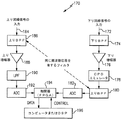
図2に示すように、障害検出および復号ユニット1は、携帯型または手持ち型のユニット20として実現されてもよい。これは、本発明の障害検出および復号ユニットの好ましい形式である。図2で示すように、ユニット20は、ヘッドエンドの上り回線の受光器7内のRFテスト地点、または、エンコーダ12の上流側の、同軸ケーブルシステム10内部の任意のテスト地点(または、他のアクセスポイント)に、接続することが出来る。
As shown in FIG. 2, the fault detection and
本発明を実施するのに好ましい方法の一般的なステップを図3に示す。第1のステップ30で、少なくとも1台のIDエンコーダ12が、同軸システム10内の符号化地点に置かれるかまたは設置されている。図1に示すように、符号化地点は、好ましくは、システム内のブランチの上流側である。第2のステップ32では、図2に示すように、障害検出および復号ユニット20を、ヘッドエンドのまたは同軸システム10内の任意のテスト地点に配置または接続する。第3のステップ34は、エンコーダ12からのIDコードを、符号化地点の下流側から発生する、上り回線周波数帯域の少なくとも一部の(雑音を含む)信号に付与する。IDコードは、好ましくは変調周波数を識別コードとする振幅変調の形をしている。第4のステップ36は、テスト地点でコード化された信号を受け取る。第5のステップ38は、ユニット20を使用して、障害がコード化された信号から検出されるかどうかを判断する。検出すべき障害は、共通の経路歪み(CPD)コード、雑音および侵入である。第6のステップ40は、ユニット20を使用して、IDコードを復号し、IDエンコーダ12および同軸システム内における符号化地点を特定することを含んでいる。IDコードが振幅変調として実現される場合には、ユニット20の復号する部分は振幅復調器である。復号化機能は、好ましくは、デジタル・シグナル・プロセサ(DSP)チップ、或いは、特定用途計算機または汎用計算機上のソフトウェアで実現される(図11および12を参照)。
The general steps of the preferred method for practicing the present invention are shown in FIG. In a
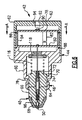
以前に示したように、IDエンコーダ12は、好ましくは、プローブの形で構成される。図4に、本発明に従って構築されたプローブ42を示す。プローブ42は、ねじ付きのコネクタ46を含み、全体として円筒形状のハウジング44、および、プローブ先端48を有する。プローブ先端48は、金属押さえコンタクト50および絶縁体アッセンブリー52を有する。図5に示されるように、プローブ42は、分配器56のアクセスポート54にねじ込まれる。分配器56は、単に例として示されている。プローブ42は、装置の押えねじの1つへの接触ができる、未使用の押えポートまたはアクセスポートを有する受動装置または能動装置の任意の種類に接続することが出来る。分配器56は、ケーブルポート58a−58dを有する。図5は、ネットワークシステム10へのプローブ42設置の簡単さを例示している。プローブ42をアクセスポート54に完全にねじ込むと、金属コンタクト50が、分配器56内部の押えねじと直接に接触する。
As indicated previously, the
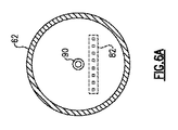
プローブ42の構造が図6および図6Aで示される。ハウジング44は、本体60およびエンドキャップ62を有し、双方は、典型的にはCATVトラップフィルタ・ハウジングに使用されるニッケルめっきした真鍮、または、同様な導電性金属で作られる。ねじ付きコネクタ46は、本体60から伸びて、ネットワークシステム上の押さえポートまたはアクセスポートにねじ込まれるように形状および寸法が形成される外ねじ64を有する。絶縁体アッセンブリー52は、全体的に円筒形状の絶縁体本体部66および円錐形の絶縁体キャップ68を備え、双方は、ポリプロピレンで作られる。絶縁体本体部66は、全体的に円形状の後部フランジ70および円筒形状のテール片72を含んでいる。プローブ先端48は、コネクタ46に挿入される。フランジ70は、挿入の間に圧縮され、プローブ本体60の肩部74に対するストッパとして働く(更に後述する)。コネクタ46への挿入を促進し、かつ、しっかりとスライドするはめ合いを確立するために、4つの縦溝が、絶縁体本体部66の外側表面上に形成されている。Oリング76は、コネクタ46とプローブ本体60との間の円周溝に取り付けられる。Oリング76は、弾性的なシール材であり、プローブ42と、プローブがねじ込まれるアクセスポートとの結合をシールするように機能する。(図5)。
The structure of the
デジタル回路基板78およびRF回路基板80は、ハウジング44に収容される。基板78および80上の回路は、図6および図6Bには示されていないが、図7および図8を参照して後述する。基板78および80は円盤状である。基板78および80は、基板配線を介して互いに接続され(更に図6Aを参照)、真鍮スペーサー84によって離される。基板78は、はんだリング86によってエンドキャップ62およびスペーサー84にはんだ付けされる。RF基板80は、別のはんだリング88によって、エンドキャップ62およびプローブ本体60にはんだ付けされる。LED90は、(図6Bに示すように)デジタル基板78の右側に搭載され、プローブ42が押さえねじと電気接触して適切に作動していることを示す表示灯として機能する。開口92が、キャップ62の後端壁63に形成され、LED90の照射線上にあって、LED90からの光がキャップ62を通して照射されることを可能にする。透明なレンズ94が開口92を封止する。
The
プローブ42の電気コンタクト組立体は、図6Bに最もよく示されている。コンタクト組立体は、ニッケルめっきした真鍮から成る押さえコンタクト先端50、有鉛のフェライトビーズ96、2重ソケットの雌の導体組立体98、および、雄のピン導体100を備える。コンタクト先端50は、絶縁体本体部66を貫通して円筒状の孔67に一部がはめ込まれる。フェライトビーズ96および導体組立体98は、孔67にはめ込まれる。コンタクト先端50は、絶縁体キャップ68によって適当な場所に固定され、絶縁体キャップは、コンタクト先端50の円周溝または肩部に係合する。フェライトビーズ96の(図6Bに示される)左側鉛は、短く切られ、コンタクト先端50の内部にはんだ付けされる。雄ピン導体100は、CATVトラップフィルタの雄導体または針に使用されたのと同じワイヤーから作られる。導体組立体98は、中空の(雌)導体ピン106および108にそれぞれはめ込まれる2つの多点バネコンタクト102および104を有する。コンタクト102および104は、米国特許第6,674,343号明細書に記載されたコンタクトと同じものである。図6Bに見られるように、コンタクト102および104は、互いに反対方向に挿入端を有する。フェライトビーズ96の右側鉛(図6B)は、コンタクト102に挿入され保持される。雌の導体ピン106および108は、円筒形状のニッケルめっきした真鍮チューブ110によって相互に連結される。ピン106および108は、好ましくはチューブ110にはんだ付けされる。図6Bに示されるように、導体組立体98は、その全体が中空状である。雄のピン100は、RF回路基板80に固定して搭載された出力端112、および、コンタクト104に挿入された入力端114を有する。このように、プローブ42がねじ込まれたネットワーク装置の押さえねじと、RF回路基板80との間で電気的接続が確立される。
The electrical contact assembly of
経験により、様々なネットワークシステム上の押さえポートまたはアクセスポートが異なる長さを持つことが知られている。従って、プローブ先端48の長さは、ポートの長さに依存して、短くするか長くするかが必要になる。これは、長さが異なるプローブの製造および品揃えを必要にする。そのような必要性は、製造者やネットワーク・オペレータに望ましい状態ではない。本発明のプローブは、ばね荷重付きプローブ先端48によって、押さえポートまたはアクセスポートにねじ込まれたときに正しい長さに自己調整することにより、上記問題を克服する。図6Bに示すように、スプリング116は、一端でテール片72に直接に取り付けられており、他端では、スプリング116は、防湿シール118に収容される円筒状くぼみ117に着座している。スプリング116は、先端48へ(図6Bの左方向に)外向きの力を与える。絶縁体本体部66は、コネクタ46の内壁表面とスライド係合している。絶縁体本体部66は、スプリング116によって外方向に、フランジ70の肩部74との係合によって停止させられる点まで押される。プローブ42が最も伸ばされた先端48よりも短い長さを有するアクセスポートにねじ込まれると、先端48は、スプリング116の力に抗して内側方向(図6Bの右方向に)に押しつけられる。先端48が内側方向へ押されても、雄ピン100は静止し、導体組立体98は、雄ピン100上をスライドする。導体組立体98の雄ピン100上におけるスライド係合は、組立体98の全体が中空であることによって可能になる。
Experience has shown that the hold down ports or access ports on various network systems have different lengths. Accordingly, the length of the
図6Bに示すように、防湿シール118は、プローブ本体60に形成された開口部120に押し込まれている。シール118および開口20はそれぞれ、2つの対応する直径を有する。シール118および開口120の大きな方の直径は、スプリング116のくぼみ117への確実な着座を可能にする。シール118および開口20の2つの直径は、また良好な湿気封止をもたらすことを支援する。シール118は、低密度ポリエチレン、ポリプロピレン、または、他の適当なシール材で作られる。シール118は、雄ピン100とシール118との接触面、および、プローブ本体60とシール118との接触面を封止する。
As shown in FIG. 6B, the moisture-
プローブ42は、同軸システム10内で、その下流側に障害が位置する位置をマークする役目をする。プローブ42は、上り回線周波数帯域(例えば5−20MHz)内の僅かな部分に、きわめてゆっくりとした且つ些細な量の(約0.2dB〜約2dBの範囲の)減衰を導入する。長い変調周期および小さな減衰値は、その存在を何れの上り回線サービスにとっても些細なものとさせるものであり、煩わしくさせるものではない。好ましくは、プローブ42は、ネットワークの平行ブランチに設置すべきであり、これによって、プローブのカスケード、および、プローブのカスケードによるネットワークに有害な効果を及ぼす上り回線の減衰が排除される。
The
プローブ42の電力供給は、同軸システム10に電力を供給するために使用される交流線電力から得られる。システム10のノードで採用される各プローブ42は、固有の特性または個人識別コードを有する。この個人識別コードは、様々な方法で形成することが出来る。例えば、単純な周波数分割が使用される場合には、各プローブ42は、自身に割り当てられた振幅変調(AM)周波数を持っていてもよい。これに代えて、符号分割または複数の方法の組合せを使用してもよい。周波数分割方法を実現することは簡単であるものの、チャンネルの数が限られている(それは個人識別コード番号の数を制限する)。更に、周波数分割方法は、必要な解読を達成するためには長い信号認識を必要とする。Gold系列またはKasami系列のような符号分割技術は、最小限のコード長および最低限の相関復号化の複雑さで、大きな組合せ数のIDを作成するのに使用できるであろう。例として、63ビットのコード長のKasami系列は、520までの数の固有のIDコードを可能にするであろう。識別コードのためにどのコード技術を選択するかは、コスト、複雑さ、および、ネットワークまたはノードに展開されるプローブやエンコーダの数などの実用的な考慮に依存する。
The power supply for the
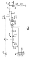
RF回路基板80に搭載された回路の回路図を図7に示す。プローブ42によって受信された信号は、(コンタクト先端50を経由し)入力124を通って基板80上の回路に入力する。電子管126およびフェライトビーズL4、L5を含む分路ブランチは、入力124とグランドとの間に接続される。電子管126は、電力サージから回路を保護する機能を有する。フェライトビーズL4およびL5は、電流サージに対処し、且つ、電子管126によって引き起こされる高周波での誤作動を減らすことを要求されている。直列インダクタL3は、入力124と阻止コンデンサーC6との間に接続される。インダクタL3は、回路を高周波から隔離する。インダクタL2およびコンデンサーC4は、AC電力を隔離抵抗R2および入力125に向けて通過させるローパス回路として機能する。出力125から得られるACパワー信号は、配線82を通って、デジタル回路基板78に供給される。図7に示すように、マイクロプロセッサー制御のスイッチ127は、阻止コンデンサーC6と阻止コンデンサーC3との間に接続される。コンデンサーC5はスイッチ127のRFlピンに接続される。
A circuit diagram of a circuit mounted on the
インピーダンス回路128は、阻止コンデンサーC3に接続される。インピーダンス回路128は、ローパス・フィルタCl、LlおよびC2、並びに、抵抗器Rlを含む。インピーダンス回路128は、上り回線周波数帯域の一部に小さな(例えば0.5dBの)減衰を与える。減衰が与えられる上り回線周波数帯域の部分は、ローパス・フィルタCl、LlおよびC2によって規定される。一実施形態では、上り回線周波数帯域の部分は約5−20MHzである。インピーダンス回路128は、上り回線周波数帯域(例えば5−20MHz)の選択された部分に、プローブ42が接続される地点のネットワーク下流側の負荷を、(例えば0.5dB)有効に低下させる。スイッチ127は、特定のプローブ42に一意に割り当てられたレートの周期で、デジタル基板78に搭載されたマイクロプロセッサーの管理下で開または閉にされる。このレートが、プローブ(従って、IDエンコーダ)のIDコードである。スイッチ127が閉であると、減衰回路128は、上り回線信号に負荷を与えて低下させる。スイッチ127が開であると、上り回線信号は影響されない。
The
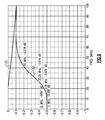
プローブ42の典型的な周波数応答プロットを図9に示す。Y軸はdBの1/10刻みの減衰を示し、X軸は0−100MHzの周波数を示す。曲線130は、減衰回路128がネットワークに切り替えられたときのプローブ42の応答を示し、曲線132は、減衰回路128が回路外に切り替えられたときの、プローブ42の応答を示す。
A typical frequency response plot for
デジタル回路基板78に搭載された回路の回路図を図8に示す。RF回路基板80からのACパワー信号は、入力129を介して受信される。抵抗器R9、コンデンサーCl、ダイオードUl、コンデンサーC2、抵抗器R3およびコンデンサーC3を含む整流器回路131は、ACパワー信号を整流されたDC信号に変換する。DC−DCコンバータ133は、整流回路131の出力と、コンデンサーC4およびC5、抵抗器R4およびコンデンサーC6を含むDCフィルタ回路135との間に接続される。マイクロプロセッサー137は、DCフィルタ回路135の出力に接続される。LED90には、バイアス抵抗器R5を介してマイクロプロセッサー137により電力が供給される。60サイクルのACパワー信号は、抵抗器R2から導入され、ツェナーダイオードダイオードU4、コンデンサーC7および抵抗器R6、R7を含む信号生成回路139に与えられる。信号生成回路139は正の正弦波信号を生成し、それはマイクロプロセッサー137のピン6に受け取られる。正弦波信号は、マイクロプロセッサー137の内部に集積されたシュミット・トリガー回路の入力に印加される。シュミット・トリガー回路は、マイクロプロセッサーのためのクロックパルスを生成する。出力クロック信号は、マイクロプロセッサー137のピン7に与えられ、出力抵抗器R8を介して基板配線82のクロックポートCLKに転送される。(RFボード上の)スイッチ127を開閉させる制御信号は、マイクロプロセッサー137のピン2および3で与えられる。これら制御信号は、基板配線82の接続部TP2およびT3を経由してRF基板80に送信される。マイクロプロセッサー137は、割り当てられたID速度でスイッチ127を切り替えるように、プログラムされる。
A circuit diagram of a circuit mounted on the
何らかの状況下では、分配器、マルチタップ、増幅器などのようなプローブ42の回路をネットワーク装置に統合することが望ましいかもしれない。それは、実行することが比較的容易であろう。
Under some circumstances, it may be desirable to integrate the circuitry of the
プローブ42がネットワークシステムに接続されると、プローブ回路がスイッチングされる周波数の帯域で、CPDまたはノイズ信号を含む如何なる信号も同様に変調される条件が成立する。存在する信号がなければ、ノイズレベルが変調されるであろう。この変調は、ゆっくりとし且つ低い減衰値であるため、送信される信号(例えば上り回線トラフィック)に対するその影響は些細である。減衰は、0.2dBと低くでき、且つ、変調周波数の信頼できる復号を可能にすることが判明した。
検出および復号の位置(ヘッドエンドの何れか、あるいはフィールド中)では、変調が検出され、個々の識別コードが解読される。一旦符号が解読されれば、このコードを備えた装置が現在どこに設置されているかの記録を調べることは単純な仕事であり、専門家が必要なトラブルシュート・プロセスを非常に単純化することを可能にする。この技術は、雑音および侵入の位置を探索するために使用できる。或いは、それは、侵入と同様に変調できるCPDの位置を解読するために、Arcom Digital Hunter(登録商標)システムのような他の装置と共に使用することが出来る。もし、CPDまたは侵入が、設置されたプローブ(エンコーダ)と同じように変調されれば、CPDまたは侵入を生成する障害の起源は、プローブ(エンコーダ)の下流に位置するに違いない。固有の変調周波数あるいは他のコードIDを要求する1つのノードに、多数のエンコーダ装置を設置することが出来る。測定をフィールド行うことが望まれる場合には、複製の装置がシステムの異なる区間に位置し、異なる区間のために個々の測定先端部がアクセス可能ならば、1つのノードで複製のコードを使用することが出来る。
When the
At the detection and decoding position (either at the headend or in the field), the modulation is detected and the individual identification codes are decoded. Once the code is deciphered, looking at the record of where the device with this code is currently installed is a simple task, and it will help the expert greatly simplify the necessary troubleshooting process. to enable. This technique can be used to search for noise and intrusion locations. Alternatively, it can be used with other devices, such as the Arcom Digital Hunter® system, to decipher the location of CPD that can be modulated as well as intrusion. If the CPD or intrusion is modulated in the same way as the installed probe (encoder), the source of the fault that generates the CPD or intrusion must be downstream of the probe (encoder). Multiple encoder devices can be installed at one node that requires a unique modulation frequency or other code ID. If it is desired to make measurements in the field, use duplicate codes at one node if duplicate devices are located in different sections of the system and individual measurement tips are accessible for different sections I can do it.
展開するプローブまたはエンコーダの数は、オペレーターの好みに依存して変動しうる。このシステムの目的に対する合理的な数は、ネットワークの各ブランチにおいて、最後の能動装置(つまり、増幅器)の後にある最初のネットワーク装置にプローブを置くことであろう。付加的な損失、カスケードされたプローブのIDを解読する際に付加された複雑さ、および、カスケードされたプローブの戻りロスに関連する不確実性のため、多数のプローブをカスケードすることは勧められない。技術的には、プローブをカスケードすることが克服できない問題を引き起こすことはないが、直列にされた多数のプローブがネットワークの性能に悪影響を及ぼす状況をもたらすことがあり得る。プローブ42は、ネットワークの電力を必要とするので、プローブ42の配置は、ネットワーク内の最も下流の位置、または、最後に電力を供給した装置の位置に置くことが予測されるであろう。そのため、各区間に1つのプローブを置くことは可能ではないかもしれない。最新のHFCシステムの典型的なノード・アーキテクチャーの分析では、1つのノードに置かれるプローブの典型的な数はおよそ20−40と示されている。設置の典型的な地点を図10に示す。図10において、同軸ケーブルネットワークシステム10は、ネットワーク・ブランチ134、136、138、140、および、142にそれぞれ設置される5つのプローブ42を備える。
The number of probes or encoders to deploy can vary depending on the operator's preference. A reasonable number for the purpose of this system would be to place the probe on the first network device after the last active device (ie, amplifier) in each branch of the network. Cascading multiple probes is recommended due to the additional loss, added complexity in decoding cascaded probe IDs, and uncertainties associated with cascaded probe return loss. Absent. Technically, cascading probes does not cause problems that cannot be overcome, but a large number of probes in series can lead to a situation that adversely affects the performance of the network. Since the
プローブが装置に取り付けられているとき、その装置の下流側の上り回線の雑音レベルおよび上り回線トラフィックは、発明者らが装置のパーソナルIDと呼ぶ、特別な変調周期に対応する固有の特性で変調される。侵入またはCPDが、プローブ位置のネットワークの下流側にある場合には、侵入またはCPDは同様に変調されるであろう。プローブの上流に位置した装置内に含まれている信号処理技術を使用することで、変調周波数またはコードを決定することができ、且つ、次いでノードに含まれる全てのプローブのパーソナルIDコードと比較することが出来るように、信号が復調またはデコードされる。その後、CPDまたは侵入が由来するネットワークの物理的なゾーンあるいは部分を、容易に見つけることができる。従って、設置されたプローブは、それぞれ明らかにマーカーになり、ネットワーク内のどこに侵入またはCPDが由来しているかを明確に指摘するであろう。各装置は、制御能力またはアドレス指定能力を必要とすることなく、独立して作動する。 When the probe is attached to a device, the upstream noise level and traffic on the downstream side of the device are modulated with unique characteristics corresponding to a special modulation period, which we call the device's personal ID. Is done. If the intrusion or CPD is downstream of the network of probe locations, the intrusion or CPD will be modulated as well. Using signal processing techniques included in the device located upstream of the probe, the modulation frequency or code can be determined and then compared to the personal ID code of all probes contained in the node The signal is demodulated or decoded so that it can. Thereafter, the physical zone or portion of the network from which the CPD or intrusion originates can be easily found. Thus, each installed probe is clearly a marker and will clearly point out where intrusion or CPD originates in the network. Each device operates independently without requiring control or addressing capabilities.
システムを実装する幾つかの方法は、自動化の希望レベルに依存して行われる。自動的にノードを監視し、CPDまたは侵入がしきい値レベルを超過するとシステム内に位置するプローブのパーソナルIDコードを計算するシステムの採用が可能である。より実際的な取組みおよび好ましい実施形態は、上り回線監視システムがヘッドエンドで採用されることである。CPDまたは雑音の状態がノード上で見られる場合には、専門家は個々のIDコードを解読するために、システムのヘッドエンド、または、或る位置の何れかで、個々のIDコードを解読する装置またはデコーダ装置を使用する。 Some methods of implementing the system are done depending on the desired level of automation. It is possible to employ a system that automatically monitors nodes and calculates a personal ID code for a probe located within the system when CPD or intrusion exceeds a threshold level. A more practical approach and preferred embodiment is that an uplink monitoring system is employed at the headend. If a CPD or noise condition is seen on the node, the expert decodes the individual ID code either at the head end of the system or at a certain location to decode the individual ID code. Use device or decoder device.
侵入信号処理に使用される装置150のブロック図を図11に示す。装置150は、まず上りテスト地点を介してネットワークに接続される。信号は入力152を介して受け取られ、次いで、増幅器154によって増幅される。その後、増幅された信号は、ローパス・フィルタ156によってろ過される。ろ過された信号は、次いでアナログ−デジタル変換器(ADC)158によってデジタル化され、次いで、デジタル・バンドパス・フィルタ(BPF)160によってろ過される。BPF160の通過帯域は、エンコーダ12(またはプローブ42)が侵入を変調する周波数帯域よりも低いか同じである。従って、もしAM変調が5−20MHzの帯域で実行されたならば、BPF160も5−20MHzであってよい。データ、遠隔測定データ、他の信号、または、搬送波が、この同じ周波数帯域内でオペレーターによって使用される場合には、BPF160はもっと狭くして、これらの信号をろ過して取り除く。BPF160の通過帯域は、(ケーブル・オペレーターの視点から見て)有用な信号がろ過によって除かれ、且つ、侵入を探索するために装置を使用する場合には、エンコーダ12(またはプローブ42)で変調された侵入の最大量が残るように選択される。より狭くCPDを探索するために装置を使用する場合には、BPF160は、「Hunter」システムでCPDをモニターするために使用される上り周波数を単に通過させればよい。
侵入源を解読するとき:
信号は、BPF160を通過した後のある時間間隔内に、2乗された侵入サンプルを連続的に合計する積分器162に入力する。積分器162の出力信号は:

When deciphering intrusion sources:
The signal is input to an
で示される。ここで、X(j)はADC158のデジタル化の合間に続く時刻TjでのBPF160の出力におけるデジタル信号の読み出し情報、Δ(Tj)=Tj−T(j−1)、Kは入力における信号デジタル化周波数と積分器162の出力との間の関係を規定する積分定数(K>1)、Nは積分器162で累算された信号X(j)サンプルの量である。
Indicated by Here, X (j) is read information of the digital signal at the output of the
信号S(i)は、信号電力の表記、すなわちより明確にはNサンプルの時間間隔上での雑音XQの平均エネルギーである。従って、積分器162は、デジタル化の時間の合間で先の時間間隔N*Δ(Tj)の雑音エネルギーが連続的に予測される雑音累積装置である。もし与えられた時間間隔が、エンコーダ12からの雑音AM変調の周期よりも短ければ、積分器162はRMS検出器として働くであろう。
The signal S (i) is a notation of signal power, more specifically the average energy of the noise XQ over a time interval of N samples. Therefore, the
信号S(i)が比較的低周波であるので、後続するデジタル処理のためのそのサンプリングは、直接の雑音源X(j)のサンプリングよりもはるかに低い周波数で行われる。装置150(図11)を具体化した装置のパラメーターの一例を挙げる。USAの典型的なHFCネットワークの5−42MHzの上り回線信号のデジタル化については、10ビットの分解度および100MHzの周波数がADC158(例えば、アナログデバイス社から利用可能なAD9215モデル)のために選択できる。BPF160および積分器162は、最新のフィールド・プログラマブル・ゲート・アレイ(FPGA)で容易に実現可能である。積分器162はピーク検出器として働くので、積分器162(または合計されたサンプルの量)における蓄積時間はできるだけ長く選ぶべきであるが、エンコーダ12(またはプローブ42)で実現し実行されるAMの最小周期よりは短く選ぶべきである。例として、エンコーダ12(またはプローブ42)の最小AM変調周期が2秒であると仮定する。積分器162の蓄積時間は0.5秒に選ぶことができる。従って、積分器162は、ノイズ信号X(J)のN=100^6*0.5または50^6(5000万)サンプルを収集すべきである。
Since the signal S (i) is relatively low frequency, its sampling for subsequent digital processing is done at a much lower frequency than the sampling of the direct noise source X (j). An example of apparatus parameters embodying the apparatus 150 (FIG. 11) will be given. For digitization of 5-42 MHz uplink signals in a typical HFC network in USA, a 10-bit resolution and 100 MHz frequency can be selected for ADC158 (eg, the AD9215 model available from Analog Devices). . The
積分器162の出力は、1Hzの周波数でAM変調された雑音エンベロープを表わす。この低周波信号をデジタル化するためには、20Hzの周波数を使用すれば十分である。従って、雑音のサンプルが10ナノ秒の周期(100MHz)で積分器162に入力している間に、積分器出力信号S(i)のサンプルは50ミリ秒の周期で得られるであろう。これはK=5^6の整数係数に相当する。これらのパラメーターの技術的な実現は容易に達成可能である。
The output of
積分器162の出力信号は、次いでコンピューターまたはデジタル・シグナル・プロセサ(DSP)164に入力する。積分器出力信号は比較的に低周波である。従って、データ伝送プロセスは問題を引き起こさないであろう。コンピューター164はAM復調に十分なデータファイル、および、対応するエンコーダ12(またはプローブ42)のIDコード検出(つまり、デコードして)を蓄積する。
The output signal of
処理を行うコンピューター164に入力する信号の最小周期は、主として、信頼できるAM信号検出および隣接するIDコード間の選択を保証することに基づいて選択すべきである。例えば、周波数符号化ID(AM周波数によるコード選択)を使用し、且つ、通常の間隔上に分配された20の符号化周波数を選択する場合には、0.5Hzから1Hzまでの帯域内では、隣接したコード周波数の間隔は0.5Hz/20=0.025Hzになる。古典的レーリー基準の使用を含むそのようなコード分割については、信号分析の最小周期を1/0.025=40秒に等しくすることが必要である。コード数の増加は、受信信号の分析に必要な継続時間を比例して長くすることに帰結する。ケーブルテレビジョン・ネットワーク内の現実の条件下では、AM信号は、侵入信号不安定によって引き起こされる様々な種類の妨害信号の状況下で受信される。従って、適切な受信を保証するためには受信信号の継続時間を増加させることが必要であろう。実際的な実現の視点から見て、信号の分析時間を厳格に固定するのではなく、それを単に数分などという適正値に制限することは合理的である。この継続時間の範囲内で、選ばれた基準(例えば信号対雑音比(SNR))によってAMコードが検出されるならば、信号受信のプロセスは容易に終了することができる。
The minimum period of the signal input to the
CPD源を解読するとき:
図12は、CPD源の位置を見つける装置170のブロック図を示す。図12は、アーコム・デジタル社の商用XcorRレーダーのブロック図に非常に似ており、同じ基本的な要素を全て含んでいる。米国出願公開US2006/0248564号(2006年11月2日公表)を参照する。それをエンコーダ12(またはプローブ42)の検出(つまり、復号化)に使用する操作上の違いは、コンピューター(またはDSP)中で実行される付加的なデータ処理アルゴリズムを加えることである。装置は以下のように作動する。下り回線信号は、入力172で装置170に入力し、次いで、バンドパス・フィルタ(BPF)174によってろ過され、QAM信号だけを含む下り回線スペクトルの一部が選択される。選択されたQAM信号は、増幅器176で増幅され、次に、CPDエミュレータ178に入力する。CPDエミュレータ178は、非線形回路素子、例えばQAM信号から二次の積を生成するダイオードを表わす。QAM信号からの二次の積は、上り回線周波数帯域(「形成されるノイズ信号」)で、実質的に一定なスペクトル密度を備えたノイズ信号を表わす。バンドパス・フィルタBPF180によって、形成されたノイズ信号スペクトルの一部の選択が実行される。選択された部分は、上り回線サービス信号がない周波数帯域である。信号スペクトルの正確に同じ部分が、上り回線信号受信(図12の左側チャンネル)のチャンネルに割り付けられる。BPF180の出力信号は、ここで「基準信号」と呼ばれる。基準信号は、アナログ・デジタル変換器182によってデジタル化される。
When decoding the CPD source:
FIG. 12 shows a block diagram of an
図12に示すように、上り回線信号は、入力184で装置170に入力し、バンドパス・フィルタ(BPF)186によってろ過される。BPF186は、BPF180と同じ周波数応答を有する。バンドパス・フィルタされた信号は、増幅器188によって増幅される。増幅器188の出力信号は、ローパス・フィルタ190によってろ過され、次いで、アナログ−デジタル変換器192によってデジタル化される。これら信号は、発明者らがCPD源からの「エコー」信号と呼ぶものを含んでいる(しかし、実際にはエコーではなく下りQAM信号からの二次混変調積である)。エコー信号は基準信号と同じであるものの、上り回線チャンネルでは、エコー信号は、ケーブルネットワーク中でCPD源への時間遅れ距離に対応する時間遅れがある。上り回線中のエコー信号検出のために、デジタル相関レシーバー194が使用される。デジタルの基準信号およびエコー信号は、デジタル相関器194(図12)に入力する。
As shown in FIG. 12, the uplink signal is input to
デジタル相関器194のブロック図を図13に示す。相関器194は、フィールド・プログラマブル・ゲート・アレイ(FPGA)で実現することが出来る。相関器194は、(基準信号を受信する)入力197と、一定幅Toのインクリメンタル遅れを持つN個のチャンネル198を有する。相関器194は、遅れのない別のチャンネル199を有する。基準信号は、可変遅延ライン200中で最小時間遅れだけ遅れる。最小時間遅れは、コンピューター196(図12)からの制御信号によって制御される。制御信号は、可変遅れライン200の入力201に入力する。チャンネル198および199はそれぞれ、乗算器202および積分器203を有する。ADC192(図12)からのエコー信号は、入力204で相関器194に入力する。エコー信号は、チャンネル198および199の各乗算器202の入力に入力する。遅延ライン200からの遅延基準信号は、チャンネル198および199に入力する。遅延基準信号は、チャンネル199の乗算器202にそれ以上の遅延なしで入力し、また、各インクリメンタル遅延ライン206により遅延を受けた後に、各チャンネル198の乗算器202に入力する。遅延ライン206は、上述のようにインクリメンタル遅れN*Toを導入する。乗算器202の出力は、積分器203によりそれぞれ積分され、その結果は、レジスタ208に格納される。積分器203の積分時間の制御、および、レジスタ208からの積分結果の読出しは、コンピューター196からのタイミング信号によって実行される。タイミング信号は、制御線207を経由して、積分器203およびレジスタ208に入力される。レジスタ208からの積分結果は、出力209を経由してコンピューター196に向かう。
A block diagram of the
チャンネル198の遅延増分Toが、概してADC182および192(図12)における信号デジタル化の周期に対応する。例えば、エコー信号受信の周波数帯域(つまり、BPF186の通過帯域)を8−16MHzの範囲に選択すると、ADC182および192のデジタル化周波数を40MHz程度に選ぶことが目的に適っている。従って、時間Toは25ナノ秒である。相関器194のチャンネル198の数、および、可変遅延ライン200の時間遅れは、CPD源からのエコー信号の遅延時間のとり得る全ての範囲が充分にカバーされるように選択される。例えば、HFCネットワーク(CPDはファイバー内では発生しない)の光ケーブル部分中の時間遅れが100マイクロ秒であり、且つ、HFCネットワークの特定ノードの同軸部分内の最大時間遅れが25マイクロ秒を超えないとすると、エコー信号の可能到着時刻とのオーバーラップを保証するためには、可変遅延ライン200の遅延時間を95マイクロ秒、相関性チャンネルの数を(10+25)マイクロ秒/To=(10+25)/0.025=1400と選ぶことが目的に適っている。
The delay increment To of
各相関チャンネルの出力からの電圧読出しは、積分器203の積分時間に同期しており、その読出しは次いでコンピューター196(図12)に転送される。エコー信号の信頼できる検出のためには、各積分器203の積分時間を20〜200ミリ秒とすべきことが実験的に確立された。全ての相関器チャンネルからの電圧読み出しは、相互相関関数を表わす信号を形成する。この信号は、中心周波数をエコー信号スペクトルの平均周波数と等しくする短時間の無線インパルスの形を有する。上記の例では、8−16MHzの周波数帯域では、中心周波数は(8+16)/2=12MHzに等しい。コンピューター196(図12)では、信号エンベロープの選択、および、選択された検出しきい値と受信した最大値との比較が実行される。
The voltage reading from the output of each correlation channel is synchronized with the integration time of
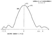
図14には、相関器194の出力における信号エンベロープの典型的形状が示されている。図14に示される信号は、チャンネルK、つまり、可変時間遅れが95マイクロ秒に設定された例で、最大の振幅を有する。エコー信号の遅延時間の測定値は、95+K*To=95+0.025Kマイクロ秒である。
FIG. 14 shows a typical shape of the signal envelope at the output of the
エコー信号が検出された後に、(相関器チャンネルKに対応する)測定された遅延時間に対応する相互相関関数エンベロープの最大振幅値が積算される。コンピューター196では、積分器203の積分時間と等しい時間間隔で相関器194からデータを受信した後に、これらの数値が作成される。エンコーダ12(またはプローブ42)がCPD源とエコー信号受信の地点との間に設置されていれば、相関器出力の最大振幅の信号は、(周波数分割IDの場合には)周波数がエンコーダまたはプローブのIDに対応する振幅変調を持つことになる。コンピューター196における最大振幅の相互相関関数の信号に対する残りの処理は、エンコーダ12(またはプローブ42)の識別(つまり、復号)のためにAM周波数を決めることである。それは、通常のスペクトル解析法によって実行することが出来る。信号読み出しに必要な積算時間は、以前に定義された侵入分析の場合に行なわれるのと同じ方法で選択される。
After the echo signal is detected, the maximum amplitude value of the cross-correlation function envelope corresponding to the measured delay time (corresponding to correlator channel K) is integrated. The
2006年11月2日に公開された特許文献1、および、2004年12月9日に公開された特許文献2は、引用によって本明細書に加入される。
発明の好ましい実施形態が、明細書に述べられ且つ図面中で特に例示されたが、本発明がこれに制限されるものではないことが理解されるであろう。添付の請求の範囲に定義された発明の精神および範囲から逸脱することなく、本発明の修正や、均等、適合が多く成されることは、当業者に明白である。 While preferred embodiments of the invention have been described in the specification and particularly illustrated in the drawings, it will be understood that the invention is not limited thereto. It will be apparent to those skilled in the art that many modifications, equivalents and adaptations can be made to the present invention without departing from the spirit and scope of the invention as defined in the appended claims.
1:障害検出および符号化ユニット
2:コンピューター
3:上り回線スイッチ
4:ヘッドエンド・コンバイナー
5:分配器
6:光送信器
7:受光器
8:光学ノード
10:同軸ケーブルシステム
10a:加入者ホーム
10b:分配増幅器
10c:分配器
10d:マルチタップ
11:タップ
12:IDエンコーダ
20:携帯障害検出/符号化ユニット
42:プローブ
44:ハウジング
46:コネクタ
48:プローブ先端
50:金属押さえコンタクト
52:絶縁体アッセンブリー
54:アクセスポート
56:分配器
58:ケーブルポート
60:プローブ本体
62:エンドキャップ
64:外ねじ
66:絶縁体本体部
68:絶縁体キャップ
70:後部フランジ
72:テール片
74:肩部
76:Oリング
78:デジタル回路基板
80:RF回路基板
82:基板配線
84:スペーサー
86:はんだリング
88:はんだリング
90:LED
92:開口
94:透明リング
96:フェライトビーズ
98:導体組立体
100:ピン導体
102:多点ばねコンタクト
104:多点ばねコンタクト
106:導体ピン
108:導体ピン
110:チューブ
112:出力端
114:入力端
116:スプリング
118:防湿シール
120:開口部
124:入力
125:入力
126:電子管
127:スイッチ
128:インピーダンス回路
131:整流器回路
133:DC−DCコンバータ
135:DCフィルタ回路
137:マイクロプロセッサー
139:信号生成回路
134、136、138、140、142:ネットワーク・ブランチ
150:信号処理装置
152:入力
154:増幅器
156:ローバス・フィルタ
158:アナログ・デジタル変換器
160:デジタル・バイパスフィルタ
162:積分器
164:コンピューター(DSP)
170:CPD源探索装置
172:入力
174:バンドパス・フィルタ
176:増幅器
178:エミュレータ
180:バンドパス・フィルタ
182:アナログ・デジタル変換器
184:入力
186:バンドパス・フィルタ
188:増幅器
190:ローパス・フィルタ
192:アナログ・デジタル変換器
194:相関器
196:コンピューター(DSP)
197:入力
198:チャンネル
199:チャンネル
200:可変遅延ライン
202:乗算器
203:積分器
204:入力
207:制御線
208:レジスタ
209:出力
1: failure detection and coding unit 2: computer 3: uplink switch 4: head end combiner 5: distributor 6: optical transmitter 7: light receiver 8: optical node 10: coaxial cable system 10a:
92: opening 94: transparent ring 96: ferrite bead 98: conductor assembly 100: pin conductor 102: multipoint spring contact 104: multipoint spring contact 106: conductor pin 108: conductor pin 110: tube 112: output end 114: input End 116: Spring 118: Dampproof seal 120: Opening 124: Input 125: Input 126: Electron tube 127: Switch 128: Impedance circuit 131: Rectifier circuit 133: DC-DC converter 135: DC filter circuit 137: Microprocessor 139:
170: CPD source search device 172: Input 174: Band pass filter 176: Amplifier 178: Emulator 180: Band pass filter 182: Analog to digital converter 184: Input 186: Band pass filter 188: Amplifier 190: Low pass Filter 192: Analog to digital converter 194: Correlator 196: Computer (DSP)
197: Input 198: Channel 199: Channel 200: Variable delay line 202: Multiplier 203: Integrator 204: Input 207: Control line 208: Register 209: Output
Claims (20)
障害の上流側にある所定の符号化地点でネットワークに接続されるように構成され、前記符号化地点の下流側で発生し前記障害に関連する信号上の識別コードを自動的に符号化する電子回路を含むエンコーダ;
前記符号化地点よりも上流側のアクセスポイントで前記ネットワークに接続されて該ネットワークから信号を受信し、該受信した信号から前記障害に関連する信号を検出して検出信号を生成する障害検出器;および
前記障害検出器に関連して配設され、前記検出信号から前記エンコーダの識別コードを復号するデコーダ、
を備え、
前記エンコーダおよび前記所定の符号化地点を特定し、前記障害の位置を前記所定の符号化地点の下流側であると判定することを特徴とするシステム。 A system for locating faults in a coaxial cable network:
An electronic device configured to be connected to a network at a predetermined encoding point upstream of a failure and automatically encoding an identification code on a signal generated downstream of the encoding point and associated with the failure An encoder including a circuit;
A fault detector that is connected to the network at an access point upstream of the encoding point, receives a signal from the network, detects a signal related to the fault from the received signal, and generates a detection signal; And a decoder arranged in association with the fault detector for decoding the encoder identification code from the detection signal,
With
The system is characterized in that the encoder and the predetermined encoding point are specified, and the position of the fault is determined to be downstream of the predetermined encoding point.
障害の上流側にある所定の符号化地点でネットワークに接続され、前記符号化地点の下流側で発生し前記障害に関連する信号上の識別コードを自動的に符号化する電子回路を含むエンコーダ;および
前記符号化地点よりも上流側のアクセスポイントで前記ネットワークに接続されて該ネットワークから信号を受信する検出およびデコーダユニット、
を備え、
前記検出およびデコーダユニットが、
前記受信した信号から前記障害に関連する信号を検出して検出信号を生成する障害検出電子回路と、
前記検出信号から前記エンコーダの識別コードを復号する復号化電子回路と、
を有し、
前記エンコーダおよび前記所定の符号化地点を特定し、前記障害の位置を前記所定の符号化地点の下流側であると判定することを特徴とするシステム。 A system for locating faults in a coaxial cable network:
An encoder that is connected to the network at a predetermined coding point upstream of the fault and includes an electronic circuit that automatically encodes an identification code on a signal generated downstream of the coding point and associated with the fault; And a detection and decoder unit connected to the network at an access point upstream of the encoding point and receiving a signal from the network;
With
The detection and decoder unit comprises:
A fault detection electronic circuit for detecting a signal related to the fault from the received signal and generating a detection signal;
A decoding electronic circuit for decoding the identification code of the encoder from the detection signal;
Have
The system is characterized in that the encoder and the predetermined encoding point are specified, and the position of the fault is determined to be downstream of the predetermined encoding point.
障害の上流側にある所定の符号化地点でネットワークに接続され、前記符号化地点の下流側で発生し前記障害に関連する信号上の識別コードを自動的に符号化するエンコーダ;
前記符号化地点よりも上流側のアクセスポイントで前記ネットワークに接続されて該ネットワークから信号を受信し、該受信した信号から前記障害に関連する信号を検出して検出信号を生成する障害検出器;および
前記障害検出器に関連して配設され、前記検出信号から前記エンコーダの識別コードを復号するデコーダ、
を備え、
前記エンコーダおよび前記所定の符号化地点を特定し、前記障害の位置を前記所定の符号化地点の下流側であると判定することを特徴とするシステム。 A system for locating faults in a coaxial cable network:
An encoder connected to the network at a predetermined coding point upstream of the fault and automatically encoding an identification code on a signal generated downstream of the coding point and associated with the fault;
A fault detector that is connected to the network at an access point upstream of the encoding point, receives a signal from the network, detects a signal related to the fault from the received signal, and generates a detection signal; And a decoder arranged in association with the fault detector for decoding the encoder identification code from the detection signal,
With
The system is characterized in that the encoder and the predetermined encoding point are specified, and the position of the fault is determined to be downstream of the predetermined encoding point.
(a)障害の上流側にある所定の符号化地点でエンコーダをネットワークに接続するステップ、
(b)前記符号化地点の下流側で発生し前記障害に関連する信号上の識別コードを自動的に符号化するステップ;
(c)前記符号化地点よりも上流側のアクセスポイントで障害検出器を前記ネットワークに接続するステップ;
(d)前記障害検出器を使用して、前記受信した信号から前記障害に関連する信号を検出して検出信号を生成するステップ;および
(e)前記検出信号から前記エンコーダの識別コードを復号するステップ、
を有し、
前記エンコーダおよび前記所定の符号化地点を特定し、前記障害の位置を前記所定の符号化地点の下流側であると判定することを特徴とする方法。 A method for locating faults within a coaxial cable network, comprising:
(A) connecting the encoder to the network at a predetermined encoding point upstream of the fault;
(B) automatically encoding an identification code on a signal generated downstream of the encoding point and associated with the fault;
(C) connecting a fault detector to the network at an access point upstream of the encoding point;
(D) using the fault detector to detect a signal associated with the fault from the received signal to generate a detection signal; and
(E) decoding the identification code of the encoder from the detection signal;
Have
A method of identifying the encoder and the predetermined encoding point, and determining that the position of the fault is downstream of the predetermined encoding point.
前記ネットワークのアクセスポイントに接続される構成および寸法を有するコネクタ部分を有するハウジング;
前記ハウジングのコネクタ部分に搭載され、絶縁部材と該絶縁部材に搭載された電気コンタクト組立体とを有するプローブ先端;および
前記ハウジングに収容され、前記電気コンタクト組立体に接続される電子回路であって、前記電気コンタクト組立体は前記コネクタ部分が前記アクセスポートに接続されたときに前記電子回路と前記ケーブルネットワークとの接続を確立し、前記電子回路は、前記ケーブルネットワークからの電力信号によって電力が供給され、前記電子回路は前記プローブに関連する識別コードを自動的に生成すると共に前記アクセスポートの下流側で発生する信号を前記識別コードによって符号化するものである電子回路、
を備え、
前記障害に関連する信号が前記識別コードで復号されると、前記障害の位置を、前記プローブが接続されている前記アクセスポートの下流側であると判定することを特徴とするプローブ。 A probe for locating a fault in a coaxial cable network:
A housing having a connector portion having a configuration and dimensions connected to an access point of the network;
A probe tip mounted on a connector portion of the housing and having an insulating member and an electrical contact assembly mounted on the insulating member; and an electronic circuit housed in the housing and connected to the electrical contact assembly. The electrical contact assembly establishes a connection between the electronic circuit and the cable network when the connector portion is connected to the access port, and the electronic circuit is powered by a power signal from the cable network. The electronic circuit automatically generates an identification code associated with the probe and encodes a signal generated downstream of the access port with the identification code;
With
When the signal related to the failure is decoded by the identification code, the position of the failure is determined to be downstream of the access port to which the probe is connected.
前記ケーブルネットワーク装置に接続されるネットワーク装置;および
前記ネットワーク装置内に搭載され前記ケーブルネットワークと電気通信する符号化回路であって、該符号化回路は前記ネットワーク装置に関連する識別コードを自動的に生成し、且つ、前記ネットワーク装置の下流側で発生する信号を前記識別コードによって符号化する符号化回路、
を備え、
前記障害と関連する信号が前記識別コードで符号化されると、前記障害の位置が前記ネットワークの下流側であると判定することを特徴とする装置。 A device that locates faults in a coaxial cable network:
A network device connected to the cable network device; and an encoding circuit mounted in the network device and in electrical communication with the cable network, wherein the encoding circuit automatically generates an identification code associated with the network device. An encoding circuit that generates and encodes a signal generated downstream of the network device with the identification code;
With
An apparatus for determining that the location of the fault is downstream of the network when a signal associated with the fault is encoded with the identification code.
Applications Claiming Priority (3)
| Application Number | Priority Date | Filing Date | Title |
|---|---|---|---|
| US94509407P | 2007-06-19 | 2007-06-19 | |
| US60/945,094 | 2007-06-19 | ||
| PCT/US2008/007624 WO2008156801A2 (en) | 2007-06-19 | 2008-06-19 | Method and apparatus for locating network impairments |
Publications (3)
| Publication Number | Publication Date |
|---|---|
| JP2010534954A JP2010534954A (en) | 2010-11-11 |
| JP2010534954A5 JP2010534954A5 (en) | 2012-11-08 |
| JP5259706B2 true JP5259706B2 (en) | 2013-08-07 |
Family
ID=39967753
Family Applications (1)
| Application Number | Title | Priority Date | Filing Date |
|---|---|---|---|
| JP2010513243A Expired - Fee Related JP5259706B2 (en) | 2007-06-19 | 2008-06-19 | Method and apparatus for searching for location of network failure |
Country Status (6)
| Country | Link |
|---|---|
| US (1) | US8458759B2 (en) |
| EP (1) | EP2188992B1 (en) |
| JP (1) | JP5259706B2 (en) |
| AT (1) | ATE497322T1 (en) |
| DE (1) | DE602008004788D1 (en) |
| WO (1) | WO2008156801A2 (en) |
Families Citing this family (34)
| Publication number | Priority date | Publication date | Assignee | Title |
|---|---|---|---|---|
| US8963689B2 (en) * | 2007-07-18 | 2015-02-24 | Jds Uniphase Corporation | Cable ID using RFID devices |
| TR201107003U1 (en) * | 2009-01-15 | 2012-07-23 | Hcs Kablolama S�Stemler� San. Ve T�C. A.�. | Improved cabling system for monitoring and managing physically connected devices on a data network |
| EP2457417A1 (en) * | 2009-07-24 | 2012-05-30 | Koninklijke Philips Electronics N.V. | Inteconnecting grids of devices of networked control systems |
| US8456530B2 (en) * | 2009-08-18 | 2013-06-04 | Arcom Digital, Llc | Methods and apparatus for detecting and locating leakage of digital signals |
| US8416697B2 (en) | 2010-02-05 | 2013-04-09 | Comcast Cable Communications, Llc | Identification of a fault |
| US8971394B2 (en) | 2010-02-05 | 2015-03-03 | Comcast Cable Communications, Llc | Inducing response signatures in a communication network |
| US9215173B1 (en) * | 2010-03-31 | 2015-12-15 | Arris Enterprises, Inc. | Fiber node discovery using ranging delay data |
| FR2959894B1 (en) * | 2010-05-07 | 2012-08-03 | Satimo Ind | SYSTEM FOR SIMULATION OF ELECTROMAGNETIC ENVIRONMENTS COMPRISING A NETWORK OF A PLURALITY OF PROBES |
| US20120170618A1 (en) * | 2011-01-04 | 2012-07-05 | ABG Tag & Traq, LLC | Ultra wideband time-delayed correlator |
| WO2012143926A1 (en) | 2011-04-18 | 2012-10-26 | HCS KABLOLAMA SISTEMLERI SAN. ve TIC.A.S. | A method of analyzing patching among panels |
| US8948596B2 (en) | 2011-07-01 | 2015-02-03 | CetusView Technologies, LLC | Neighborhood node mapping methods and apparatus for ingress mitigation in cable communication systems |
| US9398615B1 (en) * | 2011-09-07 | 2016-07-19 | Marvell International Ltd. | Carrier sensing and symbol timing in a WLAN system |
| EP2629435B1 (en) | 2012-02-16 | 2016-11-09 | Alcatel Lucent | Method and device for locating an impairment within a telecommunication line |
| US9357163B2 (en) | 2012-09-20 | 2016-05-31 | Viavi Solutions Inc. | Characterizing ingress noise |
| US10764532B2 (en) | 2012-10-30 | 2020-09-01 | Viavi Solutions Inc. | Method and system for locating ingress utilizing customer premises equipment |
| US9015786B2 (en) * | 2012-12-03 | 2015-04-21 | Comcast Cable Communications, Llc | Noise ingress detection |
| WO2014125393A2 (en) | 2013-02-18 | 2014-08-21 | Hcs Kablolama Sistemleri Sanayi Ve Ticaret A.S. | Endpoint mapping in a communication system using serial signal sensing |
| US9444719B2 (en) | 2013-03-05 | 2016-09-13 | Comcast Cable Communications, Llc | Remote detection and measurement of data signal leakage |
| US9380475B2 (en) | 2013-03-05 | 2016-06-28 | Comcast Cable Communications, Llc | Network implementation of spectrum analysis |
| EP2974041A4 (en) | 2013-03-15 | 2016-10-26 | Certusview Technologies Llc | Electro-optical apparatus and methods for upstream alignment of cable communication systems |
| US9350986B2 (en) | 2013-07-12 | 2016-05-24 | Viavi Solutions Inc. | Dual-port testing of a cable network |
| US9826263B2 (en) * | 2014-10-22 | 2017-11-21 | Arcom Digital, Llc | Detecting CPD in HFC network with OFDM signals |
| CN104754325B (en) * | 2015-02-17 | 2017-06-13 | 刘建秋 | The system and method that interference signal tape deck and cable television network damage point location |
| US9960842B2 (en) | 2015-10-12 | 2018-05-01 | Arcom Digital, Llc | Network traffic-compatible time domain reflectometer |
| US10613216B2 (en) * | 2016-05-31 | 2020-04-07 | Honeywell International Inc. | Integrated digital active phased array antenna and wingtip collision avoidance system |
| US10158423B2 (en) | 2017-01-31 | 2018-12-18 | Arcom Digital, Llc | Communicating network maintenance data in a cable system |
| US10616622B2 (en) | 2018-06-06 | 2020-04-07 | Arcom Digital Patent, Llc | Detection of CPD from signals captured at remote PHY device |
| US11082732B2 (en) | 2019-08-07 | 2021-08-03 | Arcom Digital Patent, Llc | Detection of CPD using leaked forward signal |
| US11233366B2 (en) * | 2020-03-04 | 2022-01-25 | Holland Electronics, Llc | Uninterruptable tap |
| US11335543B2 (en) * | 2020-03-25 | 2022-05-17 | Applied Materials, Inc. | RF return path for reduction of parasitic plasma |
| US20230017123A1 (en) * | 2021-07-14 | 2023-01-19 | Times Fiber Communications, Inc. | Provider equipment identification |
| EP4149076A1 (en) * | 2021-09-10 | 2023-03-15 | Vodafone GmbH | Identification of a device behind which an impairment of a network is caused |
| US12160073B1 (en) * | 2022-06-14 | 2024-12-03 | Lockheed Martin Corporation | Symmetric radio frequency coaxial splitters |
| US20240107479A1 (en) * | 2022-09-22 | 2024-03-28 | Apple Inc. | Delay Measurement for Radio-Frequency Circuitry |
Family Cites Families (27)
| Publication number | Priority date | Publication date | Assignee | Title |
|---|---|---|---|---|
| US2805399A (en) | 1955-10-04 | 1957-09-03 | William W Leeper | Connector for uniting coaxial cables |
| US5281933A (en) | 1991-10-29 | 1994-01-25 | North American Philips Corporation | Line power tapping device for cable TV distribution having a moveable module |
| US6018358A (en) * | 1994-06-09 | 2000-01-25 | Trilithic, Inc. | Radio frequency leakage detection system for CATV system |
| US5608428A (en) * | 1994-06-09 | 1997-03-04 | Trilithic, Inc. | Radio frequency leakage detection system for CATV system |
| US5505636A (en) | 1994-10-25 | 1996-04-09 | Reltec Corporation | CATV power tapping device |
| US6880170B1 (en) | 1994-11-30 | 2005-04-12 | General Instrument Corporation | Ingress detection and attenuation |
| US6292944B1 (en) | 1996-07-31 | 2001-09-18 | Trilithic, Inc. | Return path ingress in a two-way CATV system |
| US5990687A (en) | 1997-05-29 | 1999-11-23 | Williams; Thomas H. | Measuring shield breaks in coaxial cable by a sheath test current |
| JPH1193476A (en) * | 1997-09-16 | 1999-04-06 | Mazda Motor Corp | Radio correspondence device |
| US6307593B1 (en) | 1997-10-03 | 2001-10-23 | Wavetek Corporation | Pulsed leakage tagging signal |
| JP3421232B2 (en) * | 1997-11-14 | 2003-06-30 | シンクレイヤ株式会社 | CATV transmission system |
| WO2000013424A1 (en) | 1998-09-02 | 2000-03-09 | Wavetek Wandel Goltermann, Inc. | Catv return path impairment detection and location system |
| JP2000151230A (en) * | 1998-11-10 | 2000-05-30 | Kopeck Japan:Kk | Antenna system for portable communication terminal |
| US7620611B1 (en) | 1999-07-20 | 2009-11-17 | Trilithic, Inc. | Neural networks for ingress monitoring |
| US6772437B1 (en) * | 1999-07-28 | 2004-08-03 | Telefonaktiebolaget Lm Ericsson | Cable modems and systems and methods for identification of a noise signal source on a cable network |
| US6804826B1 (en) | 1999-07-28 | 2004-10-12 | Trilithic, Inc. | Radio frequency leakage detection system for CATV system |
| US6362709B1 (en) | 1999-12-21 | 2002-03-26 | Andrew Corporation | Broadband tap for extracting energy from transmission lines using impedance transformers |
| US20020144292A1 (en) | 2001-02-19 | 2002-10-03 | Jun Uemura | Bi-directional CATV system, line equipment, center equipment |
| JP2003179948A (en) * | 2001-12-10 | 2003-06-27 | Furukawa Electric Co Ltd:The | Monitoring system for CATV system |
| US20040172664A1 (en) | 2002-09-13 | 2004-09-02 | Rocci Joseph D. | Apparatus and methods to convert a legacy cable TV subscriber tap into an addressable subscriber tap |
| US7415367B2 (en) * | 2003-05-20 | 2008-08-19 | Arcom Digital, Llc | System and method to locate common path distortion on cable systems |
| JP2005123870A (en) | 2003-10-16 | 2005-05-12 | Kansai Cable Net Kk | Controller of catv system |
| US7584496B2 (en) | 2005-02-22 | 2009-09-01 | Arcom Digital, Llc | Method and apparatus for pinpointing common path distortion |
| US20060271986A1 (en) * | 2005-05-23 | 2006-11-30 | Mark Vogel | Methods, gating devices, and computer program products for determining a noise source in a communication network |
| US7167011B2 (en) * | 2005-05-27 | 2007-01-23 | Tektronix, Inc. | Differential measurement probe having retractable double cushioned variable spacing probing tips with EOS/ESD protection capabilities |
| US20070169162A1 (en) * | 2006-01-18 | 2007-07-19 | Srinivas Kola | Hierarchical communications network with upstream signal controllable from head end |
| US20070288982A1 (en) | 2006-06-13 | 2007-12-13 | Comcast Cable Holdings, Llc | Dynamic ingress arrester |
-
2008
- 2008-06-18 US US12/214,399 patent/US8458759B2/en active Active
- 2008-06-19 AT AT08779677T patent/ATE497322T1/en not_active IP Right Cessation
- 2008-06-19 JP JP2010513243A patent/JP5259706B2/en not_active Expired - Fee Related
- 2008-06-19 EP EP08779677A patent/EP2188992B1/en not_active Not-in-force
- 2008-06-19 DE DE602008004788T patent/DE602008004788D1/en active Active
- 2008-06-19 WO PCT/US2008/007624 patent/WO2008156801A2/en not_active Ceased
Also Published As
| Publication number | Publication date |
|---|---|
| ATE497322T1 (en) | 2011-02-15 |
| EP2188992B1 (en) | 2011-01-26 |
| WO2008156801A3 (en) | 2009-02-19 |
| DE602008004788D1 (en) | 2011-03-10 |
| JP2010534954A (en) | 2010-11-11 |
| EP2188992A2 (en) | 2010-05-26 |
| US20080320541A1 (en) | 2008-12-25 |
| WO2008156801A2 (en) | 2008-12-24 |
| US8458759B2 (en) | 2013-06-04 |
Similar Documents
| Publication | Publication Date | Title |
|---|---|---|
| JP5259706B2 (en) | Method and apparatus for searching for location of network failure | |
| US7254827B1 (en) | Ingress monitoring system and method | |
| US6094211A (en) | TV and data cable system ingress noise blocker | |
| US6559756B2 (en) | Ingress monitoring device in a broadband communications system | |
| US3750022A (en) | System for minimizing upstream noise in a subscriber response cable television system | |
| CN110061788B (en) | Communication device and method executed by communication device | |
| US11290761B2 (en) | Detection of CPD from signals captured at remote PHY device | |
| US9774847B2 (en) | Dual-port testing of a cable network | |
| WO1997027685A3 (en) | Packet network monitoring device | |
| US20100052658A1 (en) | Built-in test for high-speed electrical networks | |
| Leu et al. | Ultra sensitive TV detector measurements | |
| US10333616B1 (en) | Detecting burst PIM in downstream at drop | |
| US7489137B2 (en) | Power line induction of sheath test current to discover defective coaxial cable | |
| US6859828B1 (en) | Bi-directional test system for network analysis | |
| US6433905B1 (en) | Frequency agile transponder | |
| US9130785B2 (en) | Method for the detection and identification of failed electronic radio frequency (RF) transmission devices | |
| US7298396B2 (en) | Apparatus and method for monitoring transmission systems using embedded test signals | |
| US6291983B1 (en) | Selecting and monitoring signal lines with spurious transients in broadband network | |
| US20170063489A1 (en) | Inband spurious detection and processing within communication systems | |
| Showers et al. | Fundamental limits on EMC | |
| US20070268833A1 (en) | Systems and methods for measuring two or more input signals using a single input on a measuring device | |
| Williams | Proofing and Maintaining Upstream Cable Plant with Digital Signal Analysis Techniques | |
| EP2519015B1 (en) | Method of tagging signals used for leakage detection and measurement in xDSL data transmission networks and apparatus for detection and/or measurement of leakage sources tagged with this method | |
| EP0689059A1 (en) | Partial discharge detector for electric equipment | |
| Bridges et al. | Orthogonal detection to reduce common channel interference |
Legal Events
| Date | Code | Title | Description |
|---|---|---|---|
| A521 | Request for written amendment filed |
Free format text: JAPANESE INTERMEDIATE CODE: A523 Effective date: 20101007 |
|
| A621 | Written request for application examination |
Free format text: JAPANESE INTERMEDIATE CODE: A621 Effective date: 20101007 |
|
| A521 | Request for written amendment filed |
Free format text: JAPANESE INTERMEDIATE CODE: A523 Effective date: 20110526 |
|
| A977 | Report on retrieval |
Free format text: JAPANESE INTERMEDIATE CODE: A971007 Effective date: 20120516 |
|
| A131 | Notification of reasons for refusal |
Free format text: JAPANESE INTERMEDIATE CODE: A131 Effective date: 20120522 |
|
| A601 | Written request for extension of time |
Free format text: JAPANESE INTERMEDIATE CODE: A601 Effective date: 20120822 |
|
| A602 | Written permission of extension of time |
Free format text: JAPANESE INTERMEDIATE CODE: A602 Effective date: 20120829 |
|
| A524 | Written submission of copy of amendment under article 19 pct |
Free format text: JAPANESE INTERMEDIATE CODE: A524 Effective date: 20120924 |
|
| TRDD | Decision of grant or rejection written | ||
| A01 | Written decision to grant a patent or to grant a registration (utility model) |
Free format text: JAPANESE INTERMEDIATE CODE: A01 Effective date: 20130402 |
|
| A61 | First payment of annual fees (during grant procedure) |
Free format text: JAPANESE INTERMEDIATE CODE: A61 Effective date: 20130424 |
|
| FPAY | Renewal fee payment (event date is renewal date of database) |
Free format text: PAYMENT UNTIL: 20160502 Year of fee payment: 3 |
|
| R150 | Certificate of patent or registration of utility model |
Free format text: JAPANESE INTERMEDIATE CODE: R150 |
|
| LAPS | Cancellation because of no payment of annual fees |