JP5223635B2 - Semiconductor device - Google Patents
Semiconductor device Download PDFInfo
- Publication number
- JP5223635B2 JP5223635B2 JP2008309828A JP2008309828A JP5223635B2 JP 5223635 B2 JP5223635 B2 JP 5223635B2 JP 2008309828 A JP2008309828 A JP 2008309828A JP 2008309828 A JP2008309828 A JP 2008309828A JP 5223635 B2 JP5223635 B2 JP 5223635B2
- Authority
- JP
- Japan
- Prior art keywords
- wiring
- terminal
- terminals
- power supply
- speed signal
- Prior art date
- Legal status (The legal status is an assumption and is not a legal conclusion. Google has not performed a legal analysis and makes no representation as to the accuracy of the status listed.)
- Expired - Fee Related
Links
Images


Classifications
-
- H—ELECTRICITY
- H01—ELECTRIC ELEMENTS
- H01L—SEMICONDUCTOR DEVICES NOT COVERED BY CLASS H10
- H01L2224/00—Indexing scheme for arrangements for connecting or disconnecting semiconductor or solid-state bodies and methods related thereto as covered by H01L24/00
- H01L2224/01—Means for bonding being attached to, or being formed on, the surface to be connected, e.g. chip-to-package, die-attach, "first-level" interconnects; Manufacturing methods related thereto
- H01L2224/02—Bonding areas; Manufacturing methods related thereto
- H01L2224/04—Structure, shape, material or disposition of the bonding areas prior to the connecting process
- H01L2224/05—Structure, shape, material or disposition of the bonding areas prior to the connecting process of an individual bonding area
- H01L2224/0554—External layer
- H01L2224/0555—Shape
- H01L2224/05552—Shape in top view
- H01L2224/05554—Shape in top view being square
-
- H—ELECTRICITY
- H01—ELECTRIC ELEMENTS
- H01L—SEMICONDUCTOR DEVICES NOT COVERED BY CLASS H10
- H01L2224/00—Indexing scheme for arrangements for connecting or disconnecting semiconductor or solid-state bodies and methods related thereto as covered by H01L24/00
- H01L2224/01—Means for bonding being attached to, or being formed on, the surface to be connected, e.g. chip-to-package, die-attach, "first-level" interconnects; Manufacturing methods related thereto
- H01L2224/42—Wire connectors; Manufacturing methods related thereto
- H01L2224/47—Structure, shape, material or disposition of the wire connectors after the connecting process
- H01L2224/48—Structure, shape, material or disposition of the wire connectors after the connecting process of an individual wire connector
- H01L2224/4805—Shape
- H01L2224/4809—Loop shape
- H01L2224/48091—Arched
-
- H—ELECTRICITY
- H01—ELECTRIC ELEMENTS
- H01L—SEMICONDUCTOR DEVICES NOT COVERED BY CLASS H10
- H01L2224/00—Indexing scheme for arrangements for connecting or disconnecting semiconductor or solid-state bodies and methods related thereto as covered by H01L24/00
- H01L2224/01—Means for bonding being attached to, or being formed on, the surface to be connected, e.g. chip-to-package, die-attach, "first-level" interconnects; Manufacturing methods related thereto
- H01L2224/42—Wire connectors; Manufacturing methods related thereto
- H01L2224/47—Structure, shape, material or disposition of the wire connectors after the connecting process
- H01L2224/49—Structure, shape, material or disposition of the wire connectors after the connecting process of a plurality of wire connectors
- H01L2224/491—Disposition
- H01L2224/4912—Layout
- H01L2224/49171—Fan-out arrangements
-
- H—ELECTRICITY
- H01—ELECTRIC ELEMENTS
- H01L—SEMICONDUCTOR DEVICES NOT COVERED BY CLASS H10
- H01L2224/00—Indexing scheme for arrangements for connecting or disconnecting semiconductor or solid-state bodies and methods related thereto as covered by H01L24/00
- H01L2224/01—Means for bonding being attached to, or being formed on, the surface to be connected, e.g. chip-to-package, die-attach, "first-level" interconnects; Manufacturing methods related thereto
- H01L2224/42—Wire connectors; Manufacturing methods related thereto
- H01L2224/47—Structure, shape, material or disposition of the wire connectors after the connecting process
- H01L2224/49—Structure, shape, material or disposition of the wire connectors after the connecting process of a plurality of wire connectors
- H01L2224/491—Disposition
- H01L2224/4912—Layout
- H01L2224/49175—Parallel arrangements
-
- H—ELECTRICITY
- H01—ELECTRIC ELEMENTS
- H01L—SEMICONDUCTOR DEVICES NOT COVERED BY CLASS H10
- H01L2924/00—Indexing scheme for arrangements or methods for connecting or disconnecting semiconductor or solid-state bodies as covered by H01L24/00
- H01L2924/15—Details of package parts other than the semiconductor or other solid state devices to be connected
- H01L2924/151—Die mounting substrate
- H01L2924/153—Connection portion
- H01L2924/1531—Connection portion the connection portion being formed only on the surface of the substrate opposite to the die mounting surface
- H01L2924/15311—Connection portion the connection portion being formed only on the surface of the substrate opposite to the die mounting surface being a ball array, e.g. BGA
-
- H—ELECTRICITY
- H01—ELECTRIC ELEMENTS
- H01L—SEMICONDUCTOR DEVICES NOT COVERED BY CLASS H10
- H01L2924/00—Indexing scheme for arrangements or methods for connecting or disconnecting semiconductor or solid-state bodies as covered by H01L24/00
- H01L2924/30—Technical effects
- H01L2924/301—Electrical effects
- H01L2924/3011—Impedance
-
- H—ELECTRICITY
- H01—ELECTRIC ELEMENTS
- H01L—SEMICONDUCTOR DEVICES NOT COVERED BY CLASS H10
- H01L2924/00—Indexing scheme for arrangements or methods for connecting or disconnecting semiconductor or solid-state bodies as covered by H01L24/00
- H01L2924/30—Technical effects
- H01L2924/301—Electrical effects
- H01L2924/3025—Electromagnetic shielding
Description
本発明は、半導体装置に関し、詳しくは、半導体装置におけるノイズの抑制技術に関する。 The present invention relates to a semiconductor device, and more particularly to a technology for suppressing noise in a semiconductor device.
LSI(Large Scale Integration)パッケージ等の半導体パッケージの設計においては、配置ルール(配置制約)に従って、パッケージ外部との間で信号の伝送等を行うための端子の割り当て(アサイン)が行われる。例えば、高速信号(例えば、100MHz以上の信号)が入力もしくは出力される端子は、ノイズ対策として、電源端子に近接して配置するなど周りをなるべくノイズが小さい信号の端子にしてノイズの影響をうけにくくするように配置される。 In designing a semiconductor package such as an LSI (Large Scale Integration) package, terminals are assigned (assigned) for signal transmission and the like with the outside of the package in accordance with an arrangement rule (arrangement constraint). For example, a terminal to which a high-speed signal (for example, a signal of 100 MHz or higher) is input or output is subjected to the influence of noise by making it as a signal terminal with as little noise as possible, for example, by placing it close to the power supply terminal as a countermeasure against noise. It is arranged to make it difficult.
また、信号の同時動作により発生したノイズが電源ピンから信号ピンに伝播することを抑制するために、強化を施していない高インピーダンスの電源ピンに対して、強化を施した低インピーダンスの電源ピンを隣接して配置する方法が提案されている(例えば、特許文献1参照。)。 In addition, in order to prevent the noise generated by the simultaneous operation of signals from propagating from the power supply pin to the signal pin, the low impedance power supply pin that has been reinforced is applied to the high impedance power supply pin that has not been reinforced. A method of arranging them adjacent to each other has been proposed (for example, see Patent Document 1).
しかしながら、高速信号が入力もしくは出力される端子の各々に対して電源端子を1つずつ配置すると、電源端子の数が高速信号数分増えてしまい、半導体パッケージの端子数は増加する。また、高速信号が入力もしくは出力される端子の周りをノイズが小さい信号の端子にしようとすると、端子の配置に係る制約が増大し設計作業が煩雑になる。
本発明の目的は、半導体パッケージの端子数の増加を抑制しながらも信号に対するノイズの影響を低減できるようにすることである。
However, if one power supply terminal is arranged for each terminal to which high-speed signals are input or output, the number of power supply terminals increases by the number of high-speed signals, and the number of terminals of the semiconductor package increases. Further, when trying to make a terminal with a signal with low noise around a terminal to which a high-speed signal is input or output, restrictions on the arrangement of the terminal increase, and the design work becomes complicated.
An object of the present invention is to reduce the influence of noise on a signal while suppressing an increase in the number of terminals of a semiconductor package.
本発明の一観点によれば、半導体ダイとそれが搭載された基板とを有し、複数の信号端子と、半導体ダイの複数の端子と接続された複数のパッドと、複数の信号端子の内の第1の信号端子と複数のパッドの内の第1のパッドとを接続する第1の配線と、第1の信号端子と第1のパッドと第1の配線とを囲み、複数の電源端子の内の一つに接続された第2の配線とを有する半導体装置が提供される。第2の配線は、複数の電源端子の内の一つとの接続部分に対して近い側の配線幅よりも接続部分に対して遠い側の配線幅が太い。 According to one aspect of the present invention, and a semiconductor die and the substrate to which it is mounted, a plurality of signal terminals, and a plurality of which is connected to a plurality of terminals of a semi-conductor die pad, a plurality of signal terminals surrounding first wiring for connecting the first pad of the first signal terminals and a plurality of pads of the inner, the first signal terminal and the first pad and the first wiring, a plurality of power supply A semiconductor device having a second wiring connected to one of the terminals is provided. The second wiring has a wider wiring width on the side farther from the connection part than the wiring width on the side closer to the connection part with one of the plurality of power supply terminals.
第1の信号端子と第1のパッドとそれらを接続する第1の配線とを囲み、電源端子に接続された第2の配線を設けることにより、信号に対しての相互干渉を避けることができる。したがって、所定の信号を伝送する信号端子同士を隣接させて配置することが可能となり、端子数の増加を抑制しながらも信号に対するノイズの影響を低減することができる。 By providing the first surrounds the wiring, a second wiring connected to power supply terminal connected to the first signal terminal thereof and a first pad, to avoid mutual interference of the relative signal Can do. Therefore, it is possible to arrange signal terminals that transmit a predetermined signal adjacent to each other, and it is possible to reduce the influence of noise on the signal while suppressing an increase in the number of terminals.
以下、本発明の実施形態を図面に基づいて説明する。 Hereinafter, embodiments of the present invention will be described with reference to the drawings.
図1は、本発明の一実施形態に係る半導体装置(半導体パッケージ)の構成例を示す図である。図1(A)に模式的に示すように、本実施形態における半導体装置(半導体パッケージ)は、回路が形成されるとともにその回路に接続するための複数のパッドが配置された半導体ダイ(半導体チップ)11と、半導体ダイ11が搭載された基板13とを有する。
FIG. 1 is a diagram illustrating a configuration example of a semiconductor device (semiconductor package) according to an embodiment of the present invention. As schematically shown in FIG. 1A, the semiconductor device (semiconductor package) in the present embodiment has a semiconductor die (semiconductor chip) in which a circuit is formed and a plurality of pads for connection to the circuit are arranged. ) 11 and a
ダイ11のパッド15と基板13のボンディングパッド17とが、ボンディングワイヤ21により電気的に接続される。また、基板13のボンディングパッド17と端子19とが、パッケージ内配線(インターポーザ)23により電気的に接続される。端子19は、パッケージ外部との間で信号の伝送等を行ったり、電源の供給を受けたりするためのものである。なお、図1(A)においては、簡略に図示しているが、本実施形態における半導体パッケージでは、端子19は、基板13に格子状に配置されている。
The
例えば、端子19は、半導体パッケージがBGA(ボールグリッドアレイ)であればボール(バンプ)を介してパッケージ外部に接続される。また、例えば、端子19は、半導体パッケージがLGA(ランドグリッドアレイ)であればランドを介してパッケージ外部に接続され、PGA(ピングリッドアレイ)であればピンを介してパッケージ外部に接続される。
For example, if the semiconductor package is a BGA (ball grid array), the
ここで、半導体パッケージの設計においては、図2に示すような端子の割り当てが行われるのが一般的である。図2は、半導体パッケージの一部を示す平面図である。図2において、11は半導体ダイであり、13は基板である。ダイ11のパッド15と基板13のボンディングパッド17とが、ボンディングワイヤ21により接続され、基板13のボンディングパッド17と端子19とが、パッケージ内配線23により接続されている。
Here, in the design of the semiconductor package, the terminal assignment as shown in FIG. 2 is generally performed. FIG. 2 is a plan view showing a part of the semiconductor package. In FIG. 2, 11 is a semiconductor die and 13 is a substrate. The
端子19のうち、19HSは高速信号(例えば、100MHz以上の信号、高周波信号)が入出力される、あるいは入力又は出力される端子(以下、「高速信号端子」とも称す。)である。高速信号端子19HSは、高速信号へのノイズ対策として、所定のルール(制約)に従い配置される。例えば、高速信号端子19HSは、電源端子19PWに近接して配置される。電源端子19PWは、高電位側電源(例えばVdd)を供給するための電源高電位側端子、又は低電位側電源(例えばVss)を供給するための電源低電位側端子である。
Of the
また、例えば、高速信号端子19HSは、それら同士を隣接させないように、すなわち図2に示すように高速信号端子19HS間に少なくとも他の1つの端子があるように配置されたり、出力端子と隣接させないように配置されたりする。また、例えば、高速信号端子19HSは、データ系の入力端子で周辺がガードされるように配置される。 Further, for example, the high-speed signal terminals 19HS are arranged so as not to be adjacent to each other, that is, as shown in FIG. 2, there is at least one other terminal between the high-speed signal terminals 19HS, or are not adjacent to the output terminal. Or are arranged as follows. Further, for example, the high-speed signal terminal 19HS is arranged so that the periphery is guarded by a data input terminal.
このような所定のルールに従って高速信号端子19HSを配置することで、ノイズの影響を受けにくくするようにしている。しかしながら、上述した手法では、1つの高速信号端子19HSに対して、高速信号とは異なる信号に係る端子や電源端子を1つ以上割り当てなければならない。そのため、高速信号端子19HSの数の増加にともない、半導体パッケージに必要とされる端子数も増加する。 By arranging the high-speed signal terminal 19HS according to such a predetermined rule, it is made difficult to be affected by noise. However, in the above-described method, one or more terminals and power supply terminals related to signals different from the high-speed signal must be assigned to one high-speed signal terminal 19HS. Therefore, as the number of high-speed signal terminals 19HS increases, the number of terminals required for the semiconductor package also increases.
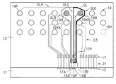
それに対して、本実施形態における半導体装置(半導体パッケージ)では、例えば、図1(B)に示すように端子の割り当てを行う。図1(B)は、図1(A)に示した半導体パッケージの一部(図1(A)に示した部分25相当)を示す平面図である。
On the other hand, in the semiconductor device (semiconductor package) in the present embodiment, for example, terminals are assigned as shown in FIG. FIG. 1B is a plan view showing a part of the semiconductor package shown in FIG. 1A (corresponding to the
図1(B)に示すように、ダイ11のパッド15と基板13のボンディングパッド17とが、ボンディングワイヤ21により接続され、基板13のボンディングパッド17と端子19とが、パッケージ内配線23により接続されている。
As shown in FIG. 1B, the
ここで、本実施形態における半導体パッケージは、高速信号(例えば100MHz以上の信号、高周波信号)に係るインタフェースを有しており、端子19A、19Bは、パッケージ外部との間で高速信号が入出力される、あるいは入力又は出力される端子(以下、「高速信号端子」とも称す。)である。本実施形態において高速信号は、例えば、クロック、DDR(Double Data Rate)−IF(interface)、SATA(Serial Advanced Technology Attachment)−IF、PCI−E(Peripheral Component Interconnect - Express)、SERDES(serializer/deserializer)、LVDS(Low Voltage Differential Signaling)などノイズに対して敏感なインタフェースからなる信号である。
Here, the semiconductor package in the present embodiment has an interface related to a high-speed signal (for example, a signal of 100 MHz or higher, a high-frequency signal), and the
高速信号端子19Aとボンディングパッド17Aとがパッケージ内配線により接続され、ボンディングパッド17Aとダイ11のパッド15Aとがボンディングワイヤにより接続される。また、高速信号端子19Aとボンディングパッド17Aとそれを接続するパッケージ内配線とを囲むようにシールド用の配線GLが形成されている。シールド用の配線GLにより閉ループが形成され、そのループ内に高速信号端子19Aとボンディングパッド17Aとそれを接続するパッケージ内配線とがある。以下、このシールド用の配線を、ガードリングとも称す。
The high-
同様に、高速信号端子19Bとボンディングパッド17Bとがパッケージ内配線により接続され、ボンディングパッド17Bとダイ11のパッド15Bとがボンディングワイヤにより接続される。また、高速信号端子19Bとボンディングパッド17Bとそれを接続するパッケージ内配線とを囲むように、ループ内に高速信号端子19Bとボンディングパッド17Bとそれを接続するパッケージ内配線とがある閉ループを形成するように、カードリングGLが形成されている。
Similarly, the high-
なお、図1(B)に示した例では、高速信号端子19Aに係るガードリングGLと、高速信号端子19Bに係るガードリングGLとは、一部の配線を共有するようにして形成されている。しかし、これに限定されるものではなく、高速信号端子19Aに係るガードリングGLと、高速信号端子19Bに係るガードリングGLとが、それぞれ独立した配線により形成されても良い。
In the example shown in FIG. 1B, the guard ring GL related to the high-
電源端子19Pは、電源高電位側端子又は電源低電位側端子である。電源高電位側端子は、パッケージ外部から高電位側電源(例えばVdd)の供給を受けてダイ11に供給するための端子である。また、電源低電位側端子は、パッケージ外部から低電位側電源(例えばVssやグランド電位)の供給を受けてダイ11に供給するための端子であり、例えばVss端子や接地(グランド)端子である。電源端子19Pとボンディングパッド17Pとがパッケージ内配線(ガードリングGLの一部)により接続され、ボンディングパッド17Pとダイ11のパッド15Pとがボンディングワイヤにより接続される。
The
高速信号端子19Aに係るガードリングGL及び高速信号端子19Bに係るガードリングGLのそれぞれは、電源端子19Pに接続される。すなわち、本実施形態では、異なる高速信号端子19A、19Bに係る複数のガードリングGLがともに電源端子19Pに接続される。
Each of the guard ring GL related to the high-
このように高速信号に対応してガードリングGLを設けることで、高速信号に対しての相互干渉を避けることができる。これにより、図1(B)に一例を示したように高速信号端子19A、19B同士を隣接させ配置することが可能となり、端子数の増加を抑制しながらも高速信号に対するノイズの影響を低減することができる。
Thus, by providing the guard ring GL corresponding to the high-speed signal, mutual interference with the high-speed signal can be avoided. As a result, as shown in FIG. 1B, the high-
また、複数の高速信号端子(図1(B)に示した例では2つの高速信号端子19A、19B)に対して、1つの電源端子19Pを対応させれば良いので、高速信号端子毎に異なる電源端子を配置させる必要がなく、端子数の増加を抑制することができる。例えば、図2に示した例と同様にして端子の割り当てを行うと、例えば端子19Xも電源端子となるが、本実施形態によれば電源端子以外の他の端子として割り当てることが可能となる。例えば、図2に示した例と同様の手法では端子19Yに割り当てられるものを、端子19Xに割り当てれば、端子19Yを設ける必要がなく、端子数の増加を抑制することができる。なお、複数のガードリングGLがともに接続される電源端子は少なくとも1つあれば良く、その数は任意であるが、端子数の増加を抑制するために対応する高速信号端子(ガードリング)の数よりも少ないことが望ましい。
Further, one
また、図2に示したような例と比較して、本実施形態によれば、端子の割り当て(アサイン)に係る配置制約(配置ルール)が緩和されて端子配置の自由度があがり、設計に係る負担を軽減することができる。
なお、図1(B)に示した例では、ボンディングパッド17に対して、ボンディングパッド17A、17Bをダイ11側に配置しているが、ダイ11に対する距離を同じにして、すべてのボンディングパッド17を配置するようにしても良い。図1(B)に示すように配置した場合には、ボンディングパッドの間隔を広げなくともガードリングGLを通すことができる。
Compared with the example shown in FIG. 2, according to the present embodiment, the arrangement restrictions (arrangement rules) related to terminal assignment (assignment) are relaxed, and the degree of freedom of terminal arrangement is increased, and the design is improved. This burden can be reduced.
In the example shown in FIG. 1B, the
ここで、ガードリングGLは、カードリングGLの位置によらず流れる電流が一定となることが好ましい。ガードリングGLの配線幅等を位置(接続される電源端子19Pに対する経路や距離)に応じて調整してインピーダンスを平均化したり、高速信号端子に接続されるパッケージ内配線23とガードリングGLとの間の距離を所定の距離に保ったりすることで、流れる電流の均一化を図ることができる。
Here, it is preferable that the current flowing through the guard ring GL is constant regardless of the position of the card ring GL. The impedance is averaged by adjusting the wiring width or the like of the guard ring GL according to the position (path or distance to the connected
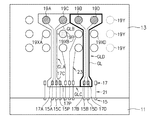
例えば、図1(B)に示したように、電源端子19Pからの距離に応じ、距離が大きくなる配線GLA、GLB、GLC、GLDの順で配線幅が太くなるようにガードリングGLの配線幅を変えればよい。例えば、電源端子19Pに対して遠い側のガードリングGLの配線幅を、電源端子19Pに対して近い側のガードリングGLの配線幅よりも太くする。このようにすることで、電源端子19Pに近い配線は単位長さあたりの抵抗値が大きく、遠くなるに従い単位長さあたりの抵抗値が小さくなり、流れる電流の均一性を改善することができる。
For example, as shown in FIG. 1B, the wiring width of the guard ring GL is increased so that the wiring width increases in the order of the wirings GLA, GLB, GLC, and GLD that increase in distance according to the distance from the
また、ガードリングGLの配線幅は、例えば次のようにして決めても良い。図1(B)に示した例では、高速信号端子19A、19Bに係るガードリングGLは、配線GLAとGLBとGLCにより1つのループを形成し、配線GLAとGLBとGLDにより1つのループを形成し、配線GLCとGLDにより1つのループを形成する。
Further, the wiring width of the guard ring GL may be determined as follows, for example. In the example shown in FIG. 1B, the guard ring GL related to the high-
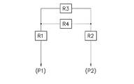
したがって、図1(B)に示したガードリングGLは、模式的に図3に示す回路図で示される。図3において、P1及びP2は、例えばボンディングパッド及び電源端子に対応する。上述した3つのループでの抵抗値が一定(略一定であっても良く、所定範囲内)になるように、すなわちR1+R2+R3=R1+R2+R4=R3+R4を満たすように、各配線GLA、GLB、GLC、GLDの抵抗値を決定する。そして、R=ρl/wt…(式1)により配線幅を決めればよい。なお、式1において、Rは抵抗値、ρは抵抗率、lは配線長(配置により決定される)、wは配線幅、tは配線厚さである。なお、配線厚さは一般的には一定であるが、配線に応じて配線厚さが調整可能である場合には配線厚さも調整するようにしても良い。また、ガードリングGLにより3つのループが形成される場合について説明したが、対応する高速信号端子の数や構成によってガードリングGLにて形成されるループの数も変わるので、形成されるループの数に応じて同様に配線幅等を求めればよい。 Therefore, the guard ring GL shown in FIG. 1B is schematically shown in the circuit diagram shown in FIG. In FIG. 3, P1 and P2 correspond to bonding pads and power supply terminals, for example. The wirings GLA, GLB, GLC, and GLD are set so that the resistance values in the three loops described above are constant (may be substantially constant and within a predetermined range), that is, satisfy R1 + R2 + R3 = R1 + R2 + R4 = R3 + R4. Determine the resistance value. Then, the wiring width may be determined by R = ρl / wt (Expression 1). In Equation 1, R is a resistance value, ρ is a resistivity, l is a wiring length (determined by arrangement), w is a wiring width, and t is a wiring thickness. The wiring thickness is generally constant, but the wiring thickness may be adjusted when the wiring thickness can be adjusted according to the wiring. In addition, although the case where three loops are formed by the guard ring GL has been described, the number of loops formed by the guard ring GL also varies depending on the number and configuration of the corresponding high-speed signal terminals. Similarly, the wiring width and the like may be obtained according to the above.
なお、図1に示した例では、高速信号端子に隣接する端子を電源端子19PとしてガードリングGLが接続されているが、これに限定されるものではない。例えば、図4に示すように、高速信号端子に隣接する端子ではなく、少なくとも1つの端子を間に挟むような近接する位置の端子を電源端子19PとしてガードリングGLを接続するようにしても良い。また、例えば、図5に示すように、高速信号端子に対して遠方に位置する端子を電源端子19PとしてガードリングGLを接続するようにしても良い。図4及び図5において、図1に示した構成要素と同一の構成要素には同一の符号を付している。
In the example shown in FIG. 1, the guard ring GL is connected with the terminal adjacent to the high-speed signal terminal as the
図4及び図5に一例を示すように、ガードリングGLが接続される電源端子の位置は任意であり、ガードリングGLが接続される電源端子の位置にかかわらず、図1に示した例と同様の効果を得ることができる。例えば、図2に示した例と同様にして端子の割り当てを行うと、例えば端子19XA、19XBは電源端子となるが、本実施形態によれば電源端子以外の他の端子として割り当てることが可能となる。また、例えば、図4及び図5に示すように、電源端子19Pからの距離に応じ、距離が大きくなる配線GLA、GLB、GLC、GLDの順で配線幅が太くなるようにガードリングGLの配線幅を変えることで、流れる電流の均一性を改善することができる。
As shown in FIG. 4 and FIG. 5 as an example, the position of the power supply terminal to which the guard ring GL is connected is arbitrary, and regardless of the position of the power supply terminal to which the guard ring GL is connected, the example shown in FIG. Similar effects can be obtained. For example, when terminals are assigned in the same manner as in the example shown in FIG. 2, for example, the terminals 19XA and 19XB become power terminals, but according to the present embodiment, they can be assigned as terminals other than the power terminals. Become. For example, as shown in FIGS. 4 and 5, the wiring of the guard ring GL so that the wiring width increases in the order of the wirings GLA, GLB, GLC, and GLD that increase in distance according to the distance from the
また、上述した説明では、シングルエンドの高速信号に関して説明したが、これに限定されるものではなく、図6に一例を示すように差動伝送される高速信号に対しても適用可能である。図6は、本実施形態における半導体装置(半導体パッケージ)のその他の構成例を示す図であり、半導体装置(半導体パッケージ)の一部を示す平面図である。 In the above description, the single-ended high-speed signal has been described. However, the present invention is not limited to this, and can be applied to a high-speed signal that is differentially transmitted as shown in FIG. FIG. 6 is a diagram showing another configuration example of the semiconductor device (semiconductor package) in the present embodiment, and is a plan view showing a part of the semiconductor device (semiconductor package).
図6に示すように、半導体ダイ11のパッド15と基板13のボンディングパッド17とが、ボンディングワイヤ21により接続され、基板13のボンディングパッド17と端子19とが、パッケージ内配線23により接続されている。端子19A、19B、19C、19Dは、高速信号端子であり、パッケージ外部との間で差動伝送される高速信号が入出力される、あるいは入力又は出力される。端子19A、19Cを介して1組の高速差動信号が伝送され、端子19B、19Dを介して他の1組の高速差動信号が伝送されるものとする。
As shown in FIG. 6, the
高速信号端子19Aとボンディングパッド17Aとがパッケージ内配線(インターポーザ)により接続され、ボンディングパッド17Aとダイ11のパッド15Aとがボンディングワイヤにより接続される。高速信号端子19Cとボンディングパッド17Cとがパッケージ内配線により接続され、ボンディングパッド17Cとダイ11のパッド15Cとがボンディングワイヤにより接続される。
The high-
また、高速信号端子19Aとボンディングパッド17Aとそれを接続するパッケージ内配線、及び高速信号端子19Cとボンディングパッド17Cとそれを接続するパッケージ内配線を囲むようにガードリングGLが形成されている。ガードリングGLは閉ループを形成し、そのループ内に高速信号端子19A、19Cとボンディングパッド17A、17Cとそれらを接続するパッケージ内配線とがある。
A guard ring GL is formed so as to surround the high-
同様に、高速信号端子19Bとボンディングパッド17Bとがパッケージ内配線により接続され、ボンディングパッド17Bとダイ11のパッド15Bとがボンディングワイヤにより接続される。高速信号端子19Dとボンディングパッド17Dとがパッケージ内配線により接続され、ボンディングパッド17Dとダイ11のパッド15Dとがボンディングワイヤにより接続される。
Similarly, the high-
また、高速信号端子19Bとボンディングパッド17Bとそれを接続するパッケージ内配線、及び高速信号端子19Dとボンディングパッド17Dとそれを接続するパッケージ内配線を囲むようにガードリングGLが形成されている。ガードリングGLは閉ループを形成し、そのループ内に高速信号端子19B、19Dとボンディングパッド17B、17Dとそれらを接続するパッケージ内配線とがある。
Further, a guard ring GL is formed so as to surround the high-
つまり、差動伝送される1組の高速信号に対して1つのガードリングが形成される点が異なるだけで、シングルエンドの高速信号の場合と同様に構成され、ガードリングがともに接続される電源端子19Pも少なくとも1つあれば良い。また、ガードリングGLが接続される電源端子の位置も任意である。このように差動伝送される高速信号に対して本実施形態を適用しても、図1に示した例と同様の効果を得ることができる。 In other words, the power source is configured in the same manner as in the case of a single-ended high-speed signal except that one guard ring is formed for a set of high-speed signals that are differentially transmitted. There may be at least one terminal 19P. The position of the power supply terminal to which the guard ring GL is connected is also arbitrary. Even when this embodiment is applied to a high-speed signal that is differentially transmitted in this way, the same effect as the example shown in FIG. 1 can be obtained.
なお、図6に示した例においても、高速信号端子19A、19Cに係るガードリングGLと、高速信号端子19B、19Dに係るガードリングGLとは、一部の配線を共有するようにして形成されているが、それぞれのガードリングGLを独立した配線により形成するようにしても良い。
In the example shown in FIG. 6, the guard ring GL related to the high-
また、上述した説明では、ガードリングGLの配線幅を抵抗値が一定となるように抵抗率を用いた計算により求める例を示したが、予め用意した配線テーブルを用いてガードリングGLの配線幅を決定するようにしても良い。半導体装置(半導体パッケージ)は、外形サイズや配線幅や配線ピッチなどルール化することができ、それらを利用して配線幅を決定することにより簡単な処理で容易に配線幅を決めることが可能である。 In the above description, the example in which the wiring width of the guard ring GL is obtained by calculation using the resistivity so that the resistance value becomes constant has been shown. However, the wiring width of the guard ring GL using a wiring table prepared in advance. May be determined. Semiconductor devices (semiconductor packages) can be ruled such as external size, wiring width, wiring pitch, etc. By using these to determine the wiring width, it is possible to easily determine the wiring width with simple processing. is there.
例えば、ガードリングGLにより形成される閉ループにおいて、電流経路(電源端子からの距離)の短い部分から離れていくにつれて配線幅を太くしていくようにする。すなわち、図7に一例を示すようにガードリングGLの配線幅が決定されるよう配線テーブルを予め用意し、それを参照して配線幅を決定する。図7に示した例では、電流経路の短い部分(基準位置とする)における配線の配線幅をGLW0とし、そこから1ボールピッチ分の距離D1だけ離れた部分における配線の配線幅をGLW1(GLW1>GLW0)とする。また、基準位置から2ボールピッチ分の距離D2だけ離れた部分における配線の配線幅をGLW2(GLW2>GLW1)とし、基準位置から3ボールピッチ分の距離D3だけ離れた部分における配線の配線幅をGLW3(GLW3>GLW2)とする。このように、基準とする位置からの距離が所定の値(例えば、ボールピッチ)の1倍、2倍、3倍、…の位置での配線幅をテーブルに規定しておき、それを基にガードリングGLの配線幅が決定されても良い。 For example, in the closed loop formed by the guard ring GL, the wiring width is increased as the distance from the short portion of the current path (distance from the power supply terminal) increases. That is, as shown in FIG. 7, a wiring table is prepared in advance so that the wiring width of the guard ring GL is determined, and the wiring width is determined with reference thereto. In the example shown in FIG. 7, the wiring width of the wiring in the short part of the current path (referred to as the reference position) is GLW0, and the wiring width of the wiring in the part separated by a distance D1 corresponding to one ball pitch is GLW1 (GLW1). > GLW0). In addition, the wiring width of the wiring in the portion separated by the distance D2 corresponding to the two-ball pitch from the reference position is GLW2 (GLW2> GLW1), and the wiring width of the wiring in the portion separated by the distance D3 corresponding to the three-ball pitch from the reference position. Assume that GLW3 (GLW3> GLW2). In this way, the wiring width at the position where the distance from the reference position is 1 time, 2 times, 3 times,... Of a predetermined value (for example, ball pitch) is defined in the table, and based on that. The wiring width of the guard ring GL may be determined.
このように配線テーブルを用いてガードリングGLの配線幅を決定するようにした場合には、煩雑な演算処理を行う必要がなく、容易に配線幅を決めることができる。また、例えばパッケージのタイプによりボールピッチ等は異なるので、絶対的な距離ではなくボールピッチ等を用いて配線テーブルを規定することで、具体的な数値を予め定義しておく必要がなく汎用性が向上される。 Thus, when the wiring width of the guard ring GL is determined using the wiring table, it is not necessary to perform complicated calculation processing, and the wiring width can be easily determined. Also, for example, the ball pitch differs depending on the type of package, so by specifying the wiring table using the ball pitch etc. instead of the absolute distance, it is not necessary to define specific numerical values in advance, and versatility is achieved. Be improved.
なお、前記実施形態は、何れも本発明を実施するにあたっての具体化のほんの一例を示したものに過ぎず、これらによって本発明の技術的範囲が限定的に解釈されてはならないものである。すなわち、本発明はその技術思想、またはその主要な特徴から逸脱することなく、様々な形で実施することができる。
本発明の諸態様を付記として以下に示す。
The above-described embodiments are merely examples of implementation in carrying out the present invention, and the technical scope of the present invention should not be construed as being limited thereto. That is, the present invention can be implemented in various forms without departing from the technical idea or the main features thereof.
Various aspects of the present invention will be described below as supplementary notes.
(付記1)
半導体ダイと、前記半導体ダイが搭載された基板とを有し、
前記基板は、
外部と信号を伝送する信号端子と、
外部より電源が供給される電源端子と、
前記半導体ダイに配置されている複数のパッドとワイヤで接続された複数のボンディングパッドと、
所定の信号を伝送する前記信号端子、当該信号端子に対応する前記ボンディングパッド、及び当該信号端子と当該ボンディングパッドとを接続する第1の配線を囲み、かつ前記電源端子に接続された第2の配線とを有することを特徴とする半導体装置。
(付記2)
前記第2の配線は、1つの前記電源端子に接続されていることを特徴とする付記1記載の半導体装置。
(付記3)
複数の前記第2の配線が、当該第2の配線の数よりも少ない数の前記電源端子にともに接続されていることを特徴とする付記1記載の半導体装置。
(付記4)
前記第2の配線は、接続された前記電源端子に対する経路及び距離の少なくとも一方に応じて配線幅が異なることを特徴とする付記1〜3の何れか1項に記載の半導体装置。
(付記5)
前記第2の配線は、接続された前記電源端子に対する距離の増加に伴って単位長さあたりの抵抗値が減少することを特徴とする付記1〜3の何れか1項に記載の半導体装置。
(付記6)
前記第2の配線は、接続された前記電源端子に対する距離の増加に伴って配線幅が太くなることを特徴とする付記1〜3の何れか1項に記載の半導体装置。
(付記7)
前記第2の配線は、接続された前記電源端子に対して遠い側の配線幅が、当該電源端子に対して近い側の配線幅より太いことを特徴とする付記1〜3の何れか1項に記載の半導体装置。
(付記8)
前記所定の信号を伝送する前記信号端子が隣接して配置され、隣接して配置された前記信号端子の間で一部を共用して、各々の前記信号端子に対応する前記第2の配線が形成されていることを特徴とする付記1〜7の何れか1項に記載の半導体装置。
(付記9)
前記所定の信号は差動信号であって、当該差動信号を伝送する1組の前記信号端子、当該1組の信号端子に対応する1組の前記ボンディングパッド、及び当該信号端子と当該ボンディングパッドとを接続する第1の配線を囲み、前記第2の配線が形成されていることを特徴とする付記1〜8の何れか1項に記載の半導体装置。
(Appendix 1)
A semiconductor die and a substrate on which the semiconductor die is mounted;
The substrate is
A signal terminal for transmitting signals with the outside;
A power supply terminal to which power is supplied from the outside;
A plurality of bonding pads connected by wires to a plurality of pads disposed on the semiconductor die;
Surrounding the signal terminal for transmitting a predetermined signal, the bonding pad corresponding to the signal terminal, and the first wiring for connecting the signal terminal and the bonding pad, and the second terminal connected to the power supply terminal A semiconductor device comprising a wiring.
(Appendix 2)
The semiconductor device according to appendix 1, wherein the second wiring is connected to one of the power supply terminals.
(Appendix 3)
The semiconductor device according to appendix 1, wherein a plurality of the second wirings are connected to a number of the power supply terminals smaller than the number of the second wirings.
(Appendix 4)
The semiconductor device according to any one of appendices 1 to 3, wherein the second wiring has a wiring width that differs according to at least one of a path and a distance to the connected power supply terminal.
(Appendix 5)
4. The semiconductor device according to claim 1, wherein a resistance value per unit length of the second wiring decreases with an increase in a distance to the connected power supply terminal.
(Appendix 6)
The semiconductor device according to any one of appendices 1 to 3, wherein the second wiring has a wiring width that increases with an increase in distance to the connected power supply terminal.
(Appendix 7)
Any one of appendices 1 to 3, wherein the second wiring has a wiring width farther from the connected power supply terminal than a wiring width closer to the power supply terminal. A semiconductor device according to 1.
(Appendix 8)
The signal terminals for transmitting the predetermined signal are arranged adjacent to each other, and a part of the signal terminals arranged adjacent to each other is shared, and the second wiring corresponding to each of the signal terminals is provided. 8. The semiconductor device according to any one of appendices 1 to 7, wherein the semiconductor device is formed.
(Appendix 9)
The predetermined signal is a differential signal, a set of the signal terminals that transmit the differential signal, a set of the bonding pads corresponding to the set of signal terminals, and the signal terminals and the bonding pads The semiconductor device according to any one of appendices 1 to 8, wherein the second wiring is formed so as to surround a first wiring that connects the first wiring and the second wiring.
11 半導体ダイ(半導体チップ)
13 基板
15 パッド
17 ボンディングパッド
19 端子
19A〜19D 信号端子
19P 電源端子
21 ボンディングワイヤ
23 インターポーザ
GL シールド用配線(ガードリング)
11 Semiconductor die (semiconductor chip)
13
Claims (4)
前記基板は、
複数の信号端子と、
外部より電源が供給される複数の電源端子と、
前記半導体ダイに配置されている複数の端子と接続された複数のパッドと、
前記複数の信号端子の内の第1の信号端子と前記複数のパッドの内の第1のパッドとを接続する第1の配線と、
前記第1の信号端子と前記第1のパッドと前記第1の配線とを囲み、前記複数の電源端子の内の一つに接続された第2の配線とを有し、
前記第2の配線は、前記複数の電源端子の内の一つとの接続部分に対して近い側の配線幅よりも前記接続部分に対して遠い側の配線幅が太いことを特徴とする半導体装置。 A semiconductor die and a substrate on which the semiconductor die is mounted;
The substrate is
Multiple signal terminals;
A plurality of power supply terminals to which power is supplied from the outside;
A plurality of paths head connected to a plurality of terminals disposed on the semiconductor die,
A first wiring connecting a first signal terminal of the plurality of signal terminals and a first pad of the plurality of pads ;
The first signal terminal and surrounds the said first pad and the first wiring, have a second wire connected to one of said plurality of power supply terminals,
The semiconductor device, wherein the second wiring has a wiring width farther from the connection portion than a wiring width closer to the connection portion to one of the plurality of power supply terminals. .
前記複数のパッドの内の第2のパッドと、
前記第2の信号端子と前記第2のパッドとを接続する第3の配線と、
前記第2の信号端子と前記第2のパッドと前記第3の配線とを囲み、前記第2の配線と一部を共用する第4の配線とを有することを特徴とする請求項1又は2に記載の半導体装置。 A second signal terminal of said first signal terminal and the adjacent said plurality of signal terminals that will be placed,
A second pad of the plurality of pads;
A third wiring connecting the second signal terminal and the second pad;
Surrounds said third wiring and the second signal terminal and the second pad, according to claim 1 or 2, characterized in that a fourth wiring sharing a part with the second wiring A semiconductor device according to 1.
Priority Applications (1)
| Application Number | Priority Date | Filing Date | Title |
|---|---|---|---|
| JP2008309828A JP5223635B2 (en) | 2008-12-04 | 2008-12-04 | Semiconductor device |
Applications Claiming Priority (1)
| Application Number | Priority Date | Filing Date | Title |
|---|---|---|---|
| JP2008309828A JP5223635B2 (en) | 2008-12-04 | 2008-12-04 | Semiconductor device |
Publications (2)
| Publication Number | Publication Date |
|---|---|
| JP2010135555A JP2010135555A (en) | 2010-06-17 |
| JP5223635B2 true JP5223635B2 (en) | 2013-06-26 |
Family
ID=42346549
Family Applications (1)
| Application Number | Title | Priority Date | Filing Date |
|---|---|---|---|
| JP2008309828A Expired - Fee Related JP5223635B2 (en) | 2008-12-04 | 2008-12-04 | Semiconductor device |
Country Status (1)
| Country | Link |
|---|---|
| JP (1) | JP5223635B2 (en) |
Cited By (1)
| Publication number | Priority date | Publication date | Assignee | Title |
|---|---|---|---|---|
| JPWO2015147058A1 (en) * | 2014-03-27 | 2017-04-13 | シチズンファインデバイス株式会社 | Pressure detection device |
Families Citing this family (3)
| Publication number | Priority date | Publication date | Assignee | Title |
|---|---|---|---|---|
| JP5390494B2 (en) * | 2010-09-14 | 2014-01-15 | ルネサスエレクトロニクス株式会社 | Semiconductor device |
| JP5764381B2 (en) * | 2011-05-09 | 2015-08-19 | 新光電気工業株式会社 | Wiring board inspection method, wiring board manufacturing method |
| JP6438792B2 (en) * | 2015-02-17 | 2018-12-19 | ルネサスエレクトロニクス株式会社 | Semiconductor device |
Family Cites Families (2)
| Publication number | Priority date | Publication date | Assignee | Title |
|---|---|---|---|---|
| JP4054188B2 (en) * | 2001-11-30 | 2008-02-27 | 富士通株式会社 | Semiconductor device |
| JP2005340741A (en) * | 2004-05-31 | 2005-12-08 | Renesas Technology Corp | Semiconductor device |
-
2008
- 2008-12-04 JP JP2008309828A patent/JP5223635B2/en not_active Expired - Fee Related
Cited By (1)
| Publication number | Priority date | Publication date | Assignee | Title |
|---|---|---|---|---|
| JPWO2015147058A1 (en) * | 2014-03-27 | 2017-04-13 | シチズンファインデバイス株式会社 | Pressure detection device |
Also Published As
| Publication number | Publication date |
|---|---|
| JP2010135555A (en) | 2010-06-17 |
Similar Documents
| Publication | Publication Date | Title |
|---|---|---|
| US10716207B2 (en) | Printed circuit board and integrated circuit package | |
| US6538336B1 (en) | Wirebond assembly for high-speed integrated circuits | |
| JP4006447B2 (en) | Semiconductor device and printed circuit board | |
| WO2017038905A1 (en) | Semiconductor device, chip module, and semiconductor module | |
| JP6429647B2 (en) | Semiconductor device | |
| KR20140024593A (en) | System package | |
| JP5223635B2 (en) | Semiconductor device | |
| US20120068339A1 (en) | VLSI Package for High Performance Integrated Circuit | |
| CN107112280B (en) | Semiconductor integrated circuit device having a plurality of semiconductor chips | |
| EP3058468B1 (en) | Receiver architecture for memory reads | |
| CN109585418B (en) | Semiconductor device and method for enhancing signal integrity of interface | |
| US20190043841A1 (en) | Semiconductor chip including a plurality of pads | |
| JP2014207462A (en) | Semiconductor device and semiconductor module | |
| US20110298118A1 (en) | Semiconductor device | |
| US7361846B2 (en) | High electrical performance semiconductor package | |
| US10313157B2 (en) | Apparatus and method for multiplexing multi-lane multi-mode data transport | |
| TW201701736A (en) | Integrated circuit, electronic device and method for transmitting data in electronic device | |
| US6933600B2 (en) | Substrate for semiconductor package | |
| US9224682B2 (en) | Semiconductor device | |
| US9837188B2 (en) | Differential return loss supporting high speed bus interfaces | |
| CN113557604A (en) | Semiconductor module and semiconductor device | |
| WO2018042518A1 (en) | Semiconductor device and printed circuit board | |
| CN112151506A (en) | Electronic packaging structure and chip thereof | |
| US20120098125A1 (en) | Integrated circuit package and physical layer interface arrangement | |
| KR100980404B1 (en) | PCB Apparatus |
Legal Events
| Date | Code | Title | Description |
|---|---|---|---|
| A621 | Written request for application examination |
Free format text: JAPANESE INTERMEDIATE CODE: A621 Effective date: 20110831 |
|
| A131 | Notification of reasons for refusal |
Free format text: JAPANESE INTERMEDIATE CODE: A131 Effective date: 20120508 |
|
| A977 | Report on retrieval |
Free format text: JAPANESE INTERMEDIATE CODE: A971007 Effective date: 20120510 |
|
| A521 | Written amendment |
Free format text: JAPANESE INTERMEDIATE CODE: A523 Effective date: 20120706 |
|
| A131 | Notification of reasons for refusal |
Free format text: JAPANESE INTERMEDIATE CODE: A131 Effective date: 20120925 |
|
| TRDD | Decision of grant or rejection written | ||
| A01 | Written decision to grant a patent or to grant a registration (utility model) |
Free format text: JAPANESE INTERMEDIATE CODE: A01 Effective date: 20130212 |
|
| A61 | First payment of annual fees (during grant procedure) |
Free format text: JAPANESE INTERMEDIATE CODE: A61 Effective date: 20130225 |
|
| R150 | Certificate of patent or registration of utility model |
Free format text: JAPANESE INTERMEDIATE CODE: R150 Ref document number: 5223635 Country of ref document: JP Free format text: JAPANESE INTERMEDIATE CODE: R150 |
|
| FPAY | Renewal fee payment (event date is renewal date of database) |
Free format text: PAYMENT UNTIL: 20160322 Year of fee payment: 3 |
|
| S111 | Request for change of ownership or part of ownership |
Free format text: JAPANESE INTERMEDIATE CODE: R313111 |
|
| R350 | Written notification of registration of transfer |
Free format text: JAPANESE INTERMEDIATE CODE: R350 |
|
| LAPS | Cancellation because of no payment of annual fees |