JP5217813B2 - Liquid crystal device and electronic device - Google Patents
Liquid crystal device and electronic device Download PDFInfo
- Publication number
- JP5217813B2 JP5217813B2 JP2008231865A JP2008231865A JP5217813B2 JP 5217813 B2 JP5217813 B2 JP 5217813B2 JP 2008231865 A JP2008231865 A JP 2008231865A JP 2008231865 A JP2008231865 A JP 2008231865A JP 5217813 B2 JP5217813 B2 JP 5217813B2
- Authority
- JP
- Japan
- Prior art keywords
- pixel
- display
- liquid crystal
- frame
- pixel electrode
- Prior art date
- Legal status (The legal status is an assumption and is not a legal conclusion. Google has not performed a legal analysis and makes no representation as to the accuracy of the status listed.)
- Active
Links
Images


Description
本発明は、例えば、時分割駆動を採用する液晶装置、及びそのような液晶装置を具備してなるプロジェクタ等の電子機器の技術分野に関する。 The present invention relates to, for example, a technical field of a liquid crystal device that employs time-division driving and an electronic apparatus such as a projector that includes such a liquid crystal device.
この種の液晶装置では、相互に隣り合う画素間で発生する横電界の影響を低減し、色再現性の高いカラー画像を表示可能な液晶表示装置が開示されている(例えば、特許文献1参照。)。 In this type of liquid crystal device, a liquid crystal display device capable of reducing the influence of a lateral electric field generated between adjacent pixels and displaying a color image with high color reproducibility is disclosed (for example, see Patent Document 1). .)
しかしながら、液晶装置によって動画を表示する場合、相互に隣り合う画素間において発生する横電界に起因して液晶の配向状態に乱れが生じてしまう。このような配向状態の乱れを消失させるために要する時間は、通常、一のフレームから当該一のフレームの次に到来する他のフレームにフレームが切り替わる時間より長い。したがって、横電界に起因して発生する液晶状態の乱れによって、動画を表示した際に生じ得る残像イメージ等の尾引きが発生してしまい、動画の表示品位を低下させてしまう。 However, when a moving image is displayed by the liquid crystal device, the alignment state of the liquid crystal is disturbed due to a lateral electric field generated between adjacent pixels. The time required to eliminate such disturbance of the orientation state is usually longer than the time for switching from one frame to another frame that arrives next to the one frame. Therefore, the liquid crystal state disturbance caused by the horizontal electric field causes tailing of an afterimage that may occur when a moving image is displayed, thereby degrading the display quality of the moving image.
よって、本発明は上記問題点等に鑑みてなされたものであり、例えば、高い表示品位で動画を表示可能な液晶装置、及びそのような液晶装置を具備してなるプロジェクタ等の電子機器を提供することを課題とする。 Therefore, the present invention has been made in view of the above problems and the like, and provides, for example, a liquid crystal device capable of displaying a moving image with high display quality, and an electronic apparatus such as a projector including such a liquid crystal device. The task is to do.
本発明の第1の発明に係る液晶装置は上記課題を解決するために、基板上の表示領域に形成された第1画素電極を有する第1画素部と、前記表示領域において前記第1画素電極に隣り合うように形成された第2画素電極を有しており、前記第1画素部と相互に共通の走査線に電気的に接続された第2画素部と、前記表示領域に表示されるべき動画の一部を構成する一枚分の単位画像を前記表示領域に表示する期間である1フレームにおいて、前記第1画素部に黒表示を行わせると共に前記第2画素部に白表示を行わせるように、前記第1画素部及び前記第2画素部を駆動する駆動回路部と、前記1フレームの一部の期間である第1サブフレームに続いて到来し、且つ、前記1フレームの半分以上の時間幅を有する第2サブフレームにおいて、前記第1画素電極及び前記第2画素電極の夫々の電位間の電位差が小さくなるように、前記駆動回路部を制御する制御手段とを備えている。 In order to solve the above problems, a liquid crystal device according to a first aspect of the present invention includes a first pixel portion having a first pixel electrode formed in a display area on a substrate, and the first pixel electrode in the display area. And a second pixel portion formed adjacent to the first pixel portion and electrically connected to a common scanning line with the first pixel portion, and displayed in the display area In one frame, which is a period for displaying one unit image constituting a part of a moving image in the display area, black display is performed on the first pixel unit and white display is performed on the second pixel unit. And a driving circuit unit for driving the first pixel unit and the second pixel unit, and a first sub-frame which is a period of a part of the one frame, and half of the one frame. In the second subframe having the above time width, As the potential difference between the respective potentials of the serial first pixel electrode and the second pixel electrode is reduced, and a control means for controlling the drive circuit section.
本発明に係る液晶装置によれば、第1画素部及び第2画素部の夫々は、例えば、基板上の表示領域を構成するようにマトリクス状に設けられた複数の画素部の一部である。第1画素部及び第2画素部の夫々は、相互に共通の走査線に電気的に接続されており、当該走査線を介して共通の走査信号を供給可能に構成されている。より具体的には、例えば、第1画素部及び第2画素部の夫々が有する画素スイッチング用素子の動作が、これら画素部間で相互に共通である走査線を介して供給された走査信号によって制御される。 According to the liquid crystal device of the present invention, each of the first pixel portion and the second pixel portion is, for example, a part of a plurality of pixel portions provided in a matrix so as to constitute a display region on the substrate. . Each of the first pixel portion and the second pixel portion is electrically connected to a common scanning line, and is configured to be able to supply a common scanning signal via the scanning line. More specifically, for example, the operation of the pixel switching element included in each of the first pixel unit and the second pixel unit is performed by a scanning signal supplied via a scanning line that is common to these pixel units. Be controlled.
駆動回路部は、例えば、走査線を介して各画素部をスイッチング制御する走査線駆動回路と、画像信号を各画素部に供給するデータ線駆動回路とを含んで構成されている。このような駆動回路部は、フレーム毎に画像信号を各画素部に供給可能に構成されている。本発明に係る液晶装置によれば、その動作時において、時間軸に沿って相連続する複数のフレームの夫々において表示領域に単位画像が順次表示される。このように連続して表示される単位画像によって動画が構成される。駆動回路部は、例えば、デジタル化された画像信号を各画素部に供給し、当該画像信号に電位に応じて画素部に白表示或いは黒表示させる。ここで、「黒表示」とは、画素部における光の透過率が略0%である状態をいい、「白表示」とは、画素部における光の透過率が略100%である状態、言い換えれば、バックライト等の光源光が液晶層を略100%透過する状態をいう。駆動回路部は、当該液晶装置の動作時において、各画素部における黒表示及び白表示の夫々が表示される表示時間の合計時間、及び組み合わせを変更することによって、表示すべき単位画像に応じて、各画素部の輝度を設定する。 The drive circuit unit includes, for example, a scan line drive circuit that performs switching control of each pixel unit via a scan line, and a data line drive circuit that supplies an image signal to each pixel unit. Such a drive circuit unit is configured to be able to supply an image signal to each pixel unit for each frame. According to the liquid crystal device of the present invention, unit images are sequentially displayed in the display area in each of a plurality of frames that are continuous along the time axis during the operation. A moving image is composed of unit images that are continuously displayed in this way. For example, the drive circuit unit supplies a digitized image signal to each pixel unit, and causes the image unit to display white or black on the pixel unit according to the potential. Here, “black display” refers to a state in which the light transmittance in the pixel portion is approximately 0%, and “white display” refers to a state in which the light transmittance in the pixel portion is approximately 100%. For example, the light source light such as a backlight is in a state of transmitting almost 100% through the liquid crystal layer. The drive circuit unit changes the total display time for displaying each of the black display and the white display in each pixel unit during the operation of the liquid crystal device, and changes the combination according to the unit image to be displayed. The brightness of each pixel unit is set.
ここで、動画の表示品位を低下させてしまう残像現象は、1フレームの後半を占める期間において、相互に隣り合う画素電極間に生じる横電界に起因して生じる液晶の配向状態の乱れが主たる原因である。したがって、制御手段は、前記1フレームの一部の期間である第1サブフレームに続いて到来し、且つ、前記1フレームの半分以上の時間幅を有する第2サブフレームにおいて、前記第1画素電極及び前記第2画素電極の夫々の電位間の電位差が小さくなるように、前記駆動回路部を制御する。 Here, the afterimage phenomenon that degrades the display quality of moving images is mainly caused by the disorder of the alignment state of the liquid crystal caused by the horizontal electric field generated between the pixel electrodes adjacent to each other in the period that occupies the second half of one frame. It is. Therefore, the control means is configured to receive the first pixel electrode in the second subframe that comes after the first subframe, which is a partial period of the one frame, and has a time width of half or more of the one frame. In addition, the driving circuit unit is controlled so that the potential difference between the respective potentials of the second pixel electrodes becomes small.
したがって、本発明に係る液晶装置によれば、相互に異なる光の透過率を有する第1画素部及び第2画素部の夫々について、第1画素電極及び前記第2画素電極の夫々の電位の電位差に起因してこれら画素電極間に生じる横電界を低減できる。よって、本発明に係る液晶装置によれば、動画が表示される際に生じ得る尾引き等の残像によって生じるディスクリネーションラインの発生を低減でき、高品位の動画を表示可能である。 Therefore, according to the liquid crystal device of the present invention, the potential difference between the potentials of the first pixel electrode and the second pixel electrode for each of the first pixel unit and the second pixel unit having different light transmittances. This can reduce the lateral electric field generated between the pixel electrodes. Therefore, according to the liquid crystal device of the present invention, it is possible to reduce the occurrence of disclination lines caused by afterimages such as tailing that may occur when a moving image is displayed, and display a high-quality moving image.
本発明の第1の発明に係る液晶装置の一の態様では、前記制御手段は、前記第2サブフレームにおいて、前記黒表示及び前記白表示の夫々を規定する2値信号のうち前記黒表示に対応する黒表示信号の電位と、前記2値信号のうち前記白表示に対応する白表示信号の電位との間の電位を有する補正済みの画像信号が前記第1画素電極及び前記第2画素電極のうち少なくとも一方の画素電極に供給されるように、前記駆動回路部を制御してもよい。 In one aspect of the liquid crystal device according to the first aspect of the present invention, the control means is configured to perform the black display among the binary signals defining the black display and the white display in the second subframe. A corrected image signal having a potential between the potential of the corresponding black display signal and the potential of the white display signal corresponding to the white display among the binary signals is the first pixel electrode and the second pixel electrode. The drive circuit unit may be controlled so as to be supplied to at least one of the pixel electrodes.
この態様によれば、第1画素電極及び第2画素電極の夫々の電位差を白表示信号の電位及び黒表示信号の電位間の電位差より小さくできる。したがって、動画を表示する際に、白表示信号の電位及び黒表示信号の電位間の電位差に起因して生じる横電界を低減でき、動画を表示した際に生じ得る残像を低減できる。 According to this aspect, the potential difference between the first pixel electrode and the second pixel electrode can be made smaller than the potential difference between the white display signal potential and the black display signal potential. Therefore, when a moving image is displayed, a lateral electric field generated due to a potential difference between the potential of the white display signal and the potential of the black display signal can be reduced, and an afterimage that can be generated when the moving image is displayed can be reduced.
本発明の第2の発明に係る液晶装置は上記課題を解決するために、基板上の表示領域に形成された第1画素電極を有する第1画素部と、前記表示領域において前記第1画素電極に隣り合うように形成された第2画素電極を有しており、前記第1画素部と相互に共通の走査線に電気的に接続された第2画素部と、前記表示領域に表示されるべき動画の一部を構成する一枚分の単位画像を前記表示領域に表示する期間である1フレームにおいて、前記第1画素部に黒表示を行わせると共に前記第2画素部に白表示を行わせるように前記第1画素部及び前記第2画素部を駆動する駆動回路部と、前記1フレームの一部の期間である第1サブフレームに続いて到来し、且つ、前記1フレームの半分以上の時間幅を有する第2サブフレームにおいて、前記第1画素電極及び前記第2画素電極の夫々の電位間の電位差が小さくなるように、前記第1画素電極及び前記第2画素電極を相互に電気的に接続している抵抗素子とを備えている。 In order to solve the above problems, a liquid crystal device according to a second aspect of the present invention has a first pixel portion having a first pixel electrode formed in a display region on a substrate, and the first pixel electrode in the display region. And a second pixel portion formed adjacent to the first pixel portion and electrically connected to a common scanning line with the first pixel portion, and displayed in the display area In one frame, which is a period for displaying one unit image constituting a part of a moving image in the display area, black display is performed on the first pixel unit and white display is performed on the second pixel unit. The driving circuit unit for driving the first pixel unit and the second pixel unit and the first sub-frame which is a period of a part of the one frame, and more than half of the one frame In the second subframe having a time width of A resistance element that electrically connects the first pixel electrode and the second pixel electrode so that a potential difference between the potentials of the first pixel electrode and the second pixel electrode is reduced. Yes.
本発明に係る液晶装置によれば、第1画素部及び第2画素部、並びに駆動回路部は、上述の液晶装置と同様の構成を有している。 According to the liquid crystal device of the present invention, the first pixel unit, the second pixel unit, and the drive circuit unit have the same configuration as the above-described liquid crystal device.
抵抗素子は、例えば、第1画素部及び第2画素部の夫々における液晶素子の抵抗値より2乃至3桁程度低い抵抗値を有しており、第2フレームにおいて前記第1画素電極及び前記第2画素電極の夫々の電位間の電位差が小さくなるように、前記第1画素電極及び前記第2画素電極を相互に電気的に接続している。より具体的には、例えば、第2フレームにおいて、黒表示に対応する画像信号が第1画素電極に供給され、白表示に対応する画像信号が第2画素電極に供給された場合、第1画素電極及び第2画素電極のうち電位の高い一方の画素電極から電位の低い他方の画素電極に電流が流れ、当該電流が流れた分、これら画素電極間の電位差が小さくなる。 The resistance element has, for example, a resistance value that is about two to three digits lower than the resistance value of the liquid crystal element in each of the first pixel portion and the second pixel portion, and the first pixel electrode and the first pixel electrode in the second frame. The first pixel electrode and the second pixel electrode are electrically connected to each other so that the potential difference between the two pixel electrodes is small. More specifically, for example, in the second frame, when an image signal corresponding to black display is supplied to the first pixel electrode and an image signal corresponding to white display is supplied to the second pixel electrode, the first pixel A current flows from one of the electrode electrodes and the second pixel electrode having a high potential to the other pixel electrode having a low potential, and the potential difference between the pixel electrodes is reduced by the amount of the current flowing.
したがって、本発明に係る液晶装置によれば、上述の第1の発明に係る液晶装置と同様に、相互に異なる光の透過率を有する第1画素部及び第2画素部の夫々について、第1画素電極及び前記第2画素電極の夫々の電位の電位差に起因してこれら画素電極間に生じる横電界を低減できる。したがって、本発明に係る液晶装置によれば、動画が表示される際に生じ得る尾引き等の残像でき、ディスクリネーションラインの発生を低減可能である。 Therefore, according to the liquid crystal device according to the present invention, as in the liquid crystal device according to the first invention described above, the first pixel unit and the second pixel unit having different light transmittances are respectively used for the first pixel unit. A lateral electric field generated between the pixel electrodes due to the potential difference between the pixel electrode and the second pixel electrode can be reduced. Therefore, according to the liquid crystal device of the present invention, afterimages such as tailing that may occur when a moving image is displayed can be generated, and the occurrence of disclination lines can be reduced.
本発明の第3の発明に係る電子機器は上記課題を解決するために、上述した本発明の第1及び第2の発明の夫々に係る液晶装置を具備してなる。 In order to solve the above problems, an electronic apparatus according to a third aspect of the present invention includes the liquid crystal device according to each of the first and second aspects of the present invention described above.
本発明に係る電子機器によれば、上述した本発明の第1及び第2の夫々に係る液晶装置を具備してなるので、残像が殆ど発生しない高品位の動画を表示が可能な、投射型表示装置、携帯電話、電子手帳、ワードプロセッサ、ビューファインダ型又はモニタ直視型のビデオテープレコーダ、ワークステーション、テレビ電話、POS端末、タッチパネルなどの各種電子機器を実現できる。また、本発明に係る電子機器として、例えば電子ペーパなどの電気泳動装置等も実現することが可能である。 According to the electronic apparatus according to the present invention, since the liquid crystal device according to each of the first and second aspects of the present invention described above is provided, a projection type capable of displaying a high-quality moving image that hardly generates an afterimage. Various electronic devices such as a display device, a mobile phone, an electronic notebook, a word processor, a viewfinder type or a monitor direct-view type video tape recorder, a workstation, a video phone, a POS terminal, and a touch panel can be realized. In addition, as an electronic apparatus according to the present invention, for example, an electrophoretic device such as electronic paper can be realized.
本発明のこのような作用及び他の利得は次に説明する実施形態から明らかにされる。 Such an operation and other advantages of the present invention will become apparent from the embodiments described below.
以下、図面を参照しながら、本発明の第1及び第2の発明に係る液晶装置、並びに、本発明の第3の発明に係る電子機器の各実施形態を説明する。 Hereinafter, embodiments of the liquid crystal device according to the first and second inventions of the present invention and the electronic apparatus according to the third invention of the present invention will be described with reference to the drawings.
<第1実施形態>
図1乃至図9を参照しながら、本発明の第1の発明に係る液晶装置の一実施形態である液晶装置1を説明する。
<First Embodiment>
A
<1−1:液晶装置の構成>
先ず、図1乃至図4を参照しながら、本実施形態に係る液晶装置1の構成を説明する。図1は、本実施形態に係る液晶装置1の電気的な構成を示したブロック図である。
<1-1: Configuration of Liquid Crystal Device>
First, the configuration of the
図1において、液晶装置1は、表示部200、駆動回路部210、及び本発明の「制御手段」の一例である制御回路部220を備えており、その動作時において、外部回路部230から駆動回路部210に供給される各種信号に応じて表示部200に画像を表示可能に構成されている。
In FIG. 1, the
表示部200は、基板上にマトリクス状に設けられた複数の画素部から構成されており、例えば、プロジェクタ等の電子機器の一部として当該電子機器に搭載された状態で、バックライト等の光源から出射された光を各画素部における液晶分子と偏光板等によって変調する。このような液晶分子に印加される電圧、即ち液晶分子を駆動するための駆動電圧は、当該液晶装置1の動作時において、表示部200を構成する各画素部に供給された画像信号に応じて設定される。尚、液晶装置1は、複数の画素部からなる表示部200の画像表示領域に画像を表示する直視型ディスプレイとして用いられてもよいし、表示部200から出射された表示光をスクリーンに投射することによって当該スクリーンに画像を表示可能なプロジェクタのライトバルブとして用いられてもよい。
The
駆動回路部210は、表示部200を構成する複数の画素部の夫々に画像信号を供給するデータ線駆動回路、及び、各画素部のオンオフをスイッチング制御する走査信号を走査線を介して表示部200に供給する走査線駆動回路等の各種回路を含んで構成された回路部である。駆動回路部210は、表示部200が動画を表示する際のフレーム毎に画像信号を各画素部に供給可能に構成されている。液晶装置1によれば、動画を表示する際に、時間軸に沿って相連続する複数のフレームの夫々において表示部200の画像表示領域に単位画像が順次表示される。このように連続して表示される単位画像によって動画が構成される。駆動回路部210は、デジタル化された画像信号を各画素部に供給し、当該画像信号に電位に応じて画素部に白表示或いは黒表示させる。ここで、「黒表示」とは、画素部における光の透過率が略0%である状態をいい、「白表示」とは、画素部における光の透過率が略100%である状態、言い換えれば、バックライト等の光源光が液晶層を略100%透過する状態をいう。駆動回路部210は、液晶装置1の動作時において、各画素部における黒表示及び白表示の夫々が表示される表示時間の合計、及び組み合わせを変更することによって、表示すべき単位画像に応じて各画素部の輝度を設定する。
The
制御回路部220は、液晶装置1の動作時において、より具体的には、表示部200に動画が表示される際に、表示部200が動画を表示する画像表示領域に尾引き等の残像が残らないように、即ちディスクリネーション等の筋状の表示不良が発生しないように、駆動回路部210を制御する。制御回路部220の動作については、後述する液晶装置の駆動方法を説明する際に詳細に説明する。
When the
次に、図2及び図3を参照しながら、液晶装置1の具体的な構成を説明する。図2は、TFTアレイ基板をその上に形成された各構成要素と共に対向基板の側から見た液晶装置1の概略的な平面図であり、図3は、図2のIII−III´断面図である。
Next, a specific configuration of the
図2及び図3において、液晶装置1では、TFTアレイ基板10と、TFTアレイ基板100に対向配置された対向基板20とを備えている。TFTアレイ基板10及び対向基板20間には液晶層50が封入されており、TFTアレイ基板10及び対向基板20は、本発明の「表示領域」の典型例である画像表示領域10aの周囲に位置するシール領域に設けられたシール材52を介して相互に接着されている。
2 and 3, the
シール材52は、両基板を貼り合わせるための、例えば紫外線硬化樹脂、熱硬化樹脂等からなり、製造プロセスにおいてTFTアレイ基板10上に塗布された後、紫外線照射、加熱等により硬化させられたものである。シール材52中には、TFTアレイ基板10と対向基板20との間隔(基板間ギャップ)を所定値とするためのグラスファイバ或いはガラスビーズ等のギャップ材が散布されている。
The sealing
シール材52が配置されたシール領域の内側に並行して、画像表示領域10aの額縁領域を規定する遮光性の額縁遮光膜53が、対向基板20側に設けられている。但し、このような額縁遮光膜53の一部又は全部は、TFTアレイ基板10側に内蔵遮光膜として設けられてもよい。
A light-shielding frame light-shielding
画像表示領域10aの周辺に位置する周辺領域のうち、シール材52が配置されたシール領域の外側に位置する領域には、データ線駆動回路101及び外部回路接続端子102がTFTアレイ基板10の一辺に沿って設けられている。また、走査線駆動回路104は、この一辺に隣接する2辺のいずれかに沿い、且つ、前記額縁遮光膜53に覆われるようにして設けられている。尚、走査線駆動回路104を、データ線駆動回路101及び外部回路接続端子102が設けられたTFTアレイ基板10の一辺に隣接する2辺に沿って設けるようにしてもよい。この場合、TFTアレイ基板10の残る一辺に沿って設けられた複数の配線によって、二つの走査線駆動回路104は互いに接続される。また。データ線駆動回路101及び走査線駆動回路104と共に、不図示の制御回路部220がTFTアレイ基板10上に形成されている。
Of the peripheral regions located around the
対向基板20の4つのコーナー部には、両基板間の上下導通端子として機能する上下導通材106が配置されている。他方、TFTアレイ基板10にはこれらのコーナー部に対向する領域において上下導通端子が設けられている。これら上下導通端子及び上下導通材106により、TFTアレイ基板10及び対向基板20間で電気的な導通をとることができる。
Vertical
図2において、TFTアレイ基板10上には、画素スイッチング用のTFTや走査線、データ線等の配線が形成された後の画素電極9a上に、配向膜が形成されている。他方、対向基板20上には、対向電極21の他、格子状又はストライプ状の遮光膜23、更には最上層部分に配向膜が形成されている。液晶層50は、例えば一種又は数種類のネマティック液晶を混合した液晶からなり、これら一対の配向膜間で、所定の配向状態をとる。
In FIG. 2, on the
次に、図4を参照しながら、表示部200の画像表示領域10aにおける電気的構成を詳細に説明する。図4は、液晶装置1が有する表示部200の画像表示領域10aにおける回路構成を示した回路図である。表示部200は、液晶装置1の画像表示領域10aを構成する複数の画素部72を備えている。複数の画素部72は、画像表示領域10aにおいて図4中のX方向及びY方向に沿ってマトリクス状に形成されている。
Next, the electrical configuration of the
画素部72は、画素電極9a、トランジスタ素子Tr、及び、液晶素子50aを備えている。トランジスタ素子Trは、例えば、画素スイッチング用TFTである。トランジスタ素子Trは、デジタル信号化された画像信号が供給されるデータ線6aと、画素電極9aとに電気的に接続されており、液晶装置1の動作時に画素電極9aをスイッチング制御する。データ線6aに書き込む画像信号S1、S2、・・・、Snは、この順に線順次に供給しても構わないし、相隣接する複数のデータ線6a同士に対して、グループ毎に供給するようにしてもよい。
The
トランジスタ素子Trのゲートに走査線3aが電気的に接続されており、液晶装置1は、所定のタイミングで、走査線3aにパルス的に走査信号G1、G2、・・・、Gmを、この順に線順次で印加するように構成されている。画素電極9aは、トランジスタ素子Trのドレインに電気的に接続されており、スイッチング素子であるトランジスタ素子Trを一定期間だけそのスイッチを閉じることにより、データ線6aから供給される画像信号S1、S2、・・・、Snが所定のタイミングで書き込まれる。画素電極9aを介して液晶に書き込まれた所定レベルの画像信号S1、S2、・・・、Snは、対向基板20に形成された対向電極との間で一定期間保持される。
The
尚、各画素部72の一部を構成する画素電極9aのうち共通の走査線に電気的に接続され、且つ図4中X方向に沿って相互に隣り合うように配置された画素電極9aの夫々が、本発明の「第1画素電極」及び「第2画素電極」の夫々の一例であり、これら画素電極9aを含んでなる画素部72の夫々が、本発明の「第1画素部」及び「第2画素部」の一例である。
Of the
液晶層50に含まれる液晶は、印加される電圧レベルにより分子集合の配向や秩序が変化することにより、光を変調し、階調表示を可能とする。本実施形態では、表示部200に供給される画像信号は、白表示及び黒表示の夫々に対応したHigh又はLowの2値の電位をとるデジタル信号である。このような画像信号は、液晶装置1の動作時に各画素電極9aに供給される。
The liquid crystal contained in the
したがって、例えば、液晶装置1がノーマリーホワイトモードで画像を表示する液晶装置であれば、Highの電位を有する画像信号が供給されると画素部72における入射光の透過率が減少し、画素部は黒表示を行う。また、液晶装置1がノーマリーブラックモードで画像を表示する液晶装置であれば、Highの電位を有する画像信号が供給されると、画素部72における入射光の透過率が増大し、画素部は白表示を行う。このような画素部72の駆動によって、液晶装置1は、画像信号に応じたコントラストを持つ光を出射できる。蓄積容量70は、固定電位線300に電気的に接続されており、画像信号がリークすることを防ぐために、画素電極9aと対向電極との間に形成される液晶素子50aと並列に付加されている。
Therefore, for example, if the
<1−2:液晶装置の駆動方法>
次に、図5乃至図8を参照しながら、液晶装置1の駆動方法を説明しつつ、液晶装置1を構成する主要な構成要素の詳細な動作を説明する。図5は、相連続するフレームの夫々において表示される白表示及び黒表示の比較例を模式的に示した模式図であり、図6は、相連続するフレームの夫々において表示される白表示及び黒表示の比較例において発生する横電界を模式的に示した模式図である。図7は、本実施形態に係る液晶装置1の駆動方法において、相連続するフレームの夫々において表示される白表示及び黒表示を模式的に示した模式図であり、図8は、本実施形態に係る液晶装置1の駆動方法において、相連続するフレームの夫々において表示される白表示及び黒表示において発生する横電界を模式的に示した模式図である。
<1-2: Driving Method of Liquid Crystal Device>
Next, detailed operations of main components constituting the
尚、図5及び図7では、画像表示領域10aにおいてマトリクス状に設けられた複数の画素部72のうち相互に同一の行に設けられ、且つ行方向に沿って連続して配列された5つの画素部における白表示及び黒表示を例に挙げており、図7及び図8では、図5及び図6に示した部分と共通する部分に共通の参照符号を付している。
In FIGS. 5 and 7, five
また、以下では、デジタル化された画像信号のうちHighレベルの画像信号の電位を固定電位線300の電位V0に対して5V高いV0+5(V)とし、Lowレベルの画像信号の電位を固定電位線300の電位V0と同電位であるV0とする。加えて、駆動方法の説明をより簡便にするために、便宜上、固定電位線300の電位V0を0(V)とし、Highレベルの画像信号が供給された画素電極9aの電位を5(V)とする。加えて、以下では、液晶装置1がノーマリーブラックモードで画像を表示する場合を例に挙げる。
In the following description, among the digitized image signals, the potential of the high-level image signal is V0 + 5 (V), which is 5V higher than the potential V0 of the fixed
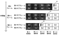
図5に示すように、液晶装置1が動画を表示した場合、時間軸に沿って順次到来する第Nフレーム、第N+1フレーム、及び第N+2フレームのうち最初に到来する第Nフレームにおいて、第(i)画素部から第(i+3)画素部までにLowレベルの画像信号が供給される。したがって、第Nフレームでは、第(i)画素部から第(i+3)画素部の夫々において、画素電極と、当該画素電極に対向する対向電極との間の液晶層50に印加される電圧は、0(V)であり、これら4つの画素部は黒表示を行う。これと並行して、第(i+4)画素部にHighレベルの画像信号が供給される。したがって、第Nフレームでは、第(i+4)画素部において、画素電極と、当該画素電極に対向する対向電極との間の液晶層50に印加される電圧は、5(V)であるため、第(i+4)画素部は白表示を行う。ここで、第Nフレームでは、相互に隣り合い、且つ、黒表示及び白表示の夫々を行っている画素部は、第(i+3)画素部及び第(i+4)画素部である。
As shown in FIG. 5, when the
第Nフレームに続いて到来する第N+1フレームでは、第(i)画素部から第(i+2)画素部までにLowレベルの画像信号が供給され、これら画素部が黒表示を行う。これと並行して、第(i+3)画素部及び第(i+4)画素部にHighレベルの画像信号が供給され、白表示が行われる。 In the (N + 1) th frame that comes after the Nth frame, a low-level image signal is supplied from the (i) pixel portion to the (i + 2) pixel portion, and these pixel portions perform black display. In parallel with this, a high-level image signal is supplied to the (i + 3) th pixel portion and the (i + 4) th pixel portion, and white display is performed.
第N+1フレームに続いて到来する第N+2フレームでは、第(i)画素部及び第(i+1)画素部にLowレベルの画像信号が供給され、これら画素部が黒表示を行う。これと並行して、第(i+2)画素部から第(i+4)画素部にHighレベルの画像信号が供給され、白表示が行われる。 In the (N + 2) th frame that comes after the (N + 1) th frame, a low level image signal is supplied to the (i) pixel portion and the (i + 1) th pixel portion, and these pixel portions perform black display. In parallel with this, a high-level image signal is supplied from the (i + 2) th pixel portion to the (i + 4) th pixel portion, and white display is performed.
第Nフレームから第N+2フレームに亘って画像表示領域10aに表示された単位画像からなる動画を見た場合、白表示及び黒表示の境界は、第(i+4)画素部及び第(i+3)画素部の境界から、第(i+2)画素部及び第(i+1)画素部の境界まで順次移動していく。
When a moving image consisting of unit images displayed in the
ここで、図6を参照しながら、相互に隣り合い、且つ黒表示及び白表示の夫々を行う2つの画素部の夫々が有する画素電極間に発生する横電界を説明する。 Here, with reference to FIG. 6, a lateral electric field generated between the pixel electrodes of the two pixel portions that are adjacent to each other and perform black display and white display will be described.
図6に示すように、液晶装置1は、TFTアレイ基板10と、TFTアレイ基板10に対向するように配置された対向基板20と、これら基板間に設けられた画素電極9a1及び9a2、並びに、配向膜16、液晶層50、配向膜22、対向電極21を備えており、相互に隣り合う画素電極9a1及び9a2の夫々の電位と、対向電極21の電位との電位差に応じた電圧が各画素電極上の液晶層50に印加されることによって、液晶層50による光の変調が可能となっている。白表示及び黒表示の夫々を行い、且つ相互の隣り合う画素部の夫々に設けられた画素電極9a1及び9a2の夫々の電位は、V0、及びV0+5(V)であり、これら画素電極間の電位差は、5(V)である。したがって、画素電極9a1及び9a2間には、5(V)の電圧に対応する電界強度を持った横電界Eが作用し、液晶分子の配向状態に乱れを生じさせてしまう。このような液晶分子の配向状態の乱れによれば、画像表示領域10aに動画が表示された際、ディスクリネーションを発生させてしまい、動画の表示品位を低下させてしまう。より具体的には、図5に示すように、白表示及び黒表示の夫々を行う2つの画素部の境界に近い領域に、縞状の残像90を発生させてしまう。そこで、液晶装置1は、次に説明するように、液晶装置1に特有の構成によって実行可能な液晶装置の駆動方法によって、縞状の残像90を低減する。
As shown in FIG. 6, the
図7及び図8を参照しながら、本実施形態に係る液晶装置1を駆動する駆動方法を説明する。
A driving method for driving the
図7及び図8に示すように、液晶装置1によれば、制御回路部220は、各々が本発明の「1フレーム」の一例である第Nフレーム、第N+1フレーム、及び第N+2フレームの夫々の一部の期間である第1サブフレームに続いて到来し、且つ、第Nフレーム、第N+1フレーム、及び第N+2フレームの夫々の半分以上の時間幅を有する第2サブフレームにおいて、画素電極9a1及び画素電極9a2の夫々の電位間の電位差が小さくなるように駆動回路部210を制御することによって、残像90を低減可能である。
As shown in FIG. 7 and FIG. 8, according to the
より具体的には、制御回路部220は、第Nフレーム、第N+1フレーム、及び第N+2フレームの夫々の第2サブフレームにおいて、黒表示及び白表示の夫々を規定する画像信号の電位を補正することによって補正済みの画像信号をデータ線駆動回路101から出力させるように、データ線駆動回路101を制御すると共に、1つのフレームにおいて第1サブフレーム及び第2サブフレームの夫々において各画素部に補正済みの画像信号が供給可能となるように、走査線駆動回路104を制御する。
More specifically, the
図7に示すように、制御回路部220は、第Nフレームの第2サブフレームにおいて第
黒表示に対応する補正済みの画像信号である黒表示信号が第(i+3)画素部に供給されるように、駆動回路部210を制御する。これと同様に、第N+1フレーム、及び第N+2フレームの夫々における第2サブフレームにおいて、制御回路部220の制御下における駆動回路部210の動作によって、第(i+2)画素部、及び、第(i+1)画素部の夫々に補正済みの画像信号である黒画像信号が供給される。ここで、黒画像信号は、例えば、画素電極の電位を0Vに設定する補正前の画像信号に比べて、電位が高められた信号であり、その電位は、Lowレベルの画像信号の電位である0(V)から、白表示に対応した画像信号の電位である5(V)までの範囲に含まれる1(V)である。
As shown in FIG. 7, the
したがって、図8に示すように、相互に隣り合い、且つ白表示及び黒表示の夫々を行う画素部に設けられた画素電極9a1及び9a2の夫々の電位は、各フレームの一部を占める第2サブフレームにおいて、1(V)及び5(V)の夫々に設定され、これら画素電極間の電位差は、5(V)より小さい4(V)になる。したがって、横電界Eの大きさは、画像信号を補正しない場合に作用する横電界Eの大きさ(5(V))より小さい4(V)になる。よって、図7に示すように、残像90に比べて筋状の残像91を低減できる。
Therefore, as shown in FIG. 8, the potentials of the pixel electrodes 9a1 and 9a2 provided in the pixel portions that are adjacent to each other and perform white display and black display respectively occupy part of each frame. In the sub-frame, 1 (V) and 5 (V) are set, and the potential difference between these pixel electrodes is 4 (V) which is smaller than 5 (V). Therefore, the magnitude of the horizontal electric field E is 4 (V), which is smaller than the magnitude (5 (V)) of the horizontal electric field E that acts when the image signal is not corrected. Therefore, as shown in FIG. 7, the
このように液晶装置1によれば、動画を表示する際に生じる可能性がある尾引きに起因するディスクリネーションライン等の表示不良を低減でき、動画の表示品位を高めることが可能である。
Thus, according to the
(変形例)
次に、図9を参照しながら、第1実施形態に係る液晶装置1が実行可能な液晶装置の駆動方法の変形例を説明する。図9は、本例に係る液晶装置の駆動方法において、相連続するフレームの夫々において表示される白表示及び黒表示を模式的に示した模式図である。
(Modification)
Next, a modification of the driving method of the liquid crystal device that can be executed by the
図9に示すように、液晶装置1によれば、制御回路部220は、各フレームの第2サブフレームにおいて、前記黒表示及び前記白表示の夫々を規定するLowレベル及びHighレベルの夫々の電位を有する画像信号のうち黒表示に対応する黒表示信号の電位と、白表示に対応する白表示信号の電位との間の電位を有する補正済みの画像信号が、画素電極9a1及び画素電極9a2のうち少なくとも一方の画素電極に供給されるように、駆動回路部210を制御する。
As shown in FIG. 9, according to the
より具体的には、第Nフレームの第2サブフレームにおいて、第(i+3)画素部に1(V)の電位を有する補正済みの画像信号が供給され、第(i+4)画素部の4(V)の電位を有する画像信号が供給される。ここで、例えば、第(i+3)画素部が有する画素電極を画素電極9a1とし、第(i+4)画素部が有する画素電極を画素電極9a2とすると、画素電極9a1及び9a2間の作用する横電界Eの大きさは、3(V)になる。したがって、画像信号を補正しない場合に比べて、横電界Eを小さくできる。同様に、第N+1フレーム、及び第N+3フレームの夫々の第2サブフレームにおいても、相互に隣り合い、且つ黒表示及び白表示を行う2つの画素部である第(i+2)画素部及び第(i+3)画素部と、第(i+1)画素部及び第(i+2)画素部との夫々に補正済みの画像信号が供給される。 More specifically, in the second subframe of the Nth frame, a corrected image signal having a potential of 1 (V) is supplied to the (i + 3) th pixel portion, and 4 (V) of the (i + 4) th pixel portion. ) Is supplied. Here, for example, assuming that the pixel electrode of the (i + 3) th pixel portion is a pixel electrode 9a1, and the pixel electrode of the (i + 4) th pixel portion is a pixel electrode 9a2, a lateral electric field E acting between the pixel electrodes 9a1 and 9a2. Is 3 (V). Therefore, the lateral electric field E can be reduced as compared with the case where the image signal is not corrected. Similarly, in each of the second subframes of the (N + 1) th frame and the (N + 3) th frame, the (i + 2) th pixel unit and the (i + 3) th pixel unit which are adjacent to each other and perform black display and white display. ) The corrected image signal is supplied to each of the pixel unit, the (i + 1) th pixel unit, and the (i + 2) th pixel unit.
したがって、本例に係る液晶装置の駆動方法によれば、相互の隣り合う画素電極9a1及び9a2間に作用する横電界を低減できるため、横電界によって生じる液晶分子の配向状態の乱れを低減でき、ディスクリネーションライン等の表示不良を低減可能である。 Therefore, according to the driving method of the liquid crystal device according to the present example, since the lateral electric field acting between the adjacent pixel electrodes 9a1 and 9a2 can be reduced, the disorder of the alignment state of the liquid crystal molecules caused by the lateral electric field can be reduced. Display defects such as disclination lines can be reduced.
尚、補正済みの画像信号は、画素電極9a1及び画素電極9a2のうち少なくとも一方の画素電極に供給されていれば横電界による筋状の残像を低減することが可能である。 In addition, if the corrected image signal is supplied to at least one of the pixel electrode 9a1 and the pixel electrode 9a2, a streaky afterimage due to a lateral electric field can be reduced.
<第2実施形態>
次に、図10及び図11を参照しながら、本発明の第2の発明に係る液晶装置の一実施形態である液晶装置500を説明する。尚、本実施形態に係る液晶装置500は、上述の第1実施形態に係る液晶装置1が備える制御回路部220に代えて、各画素電極を相互に電気的に接続する抵抗素子を備えている点に特徴を有している。したがって、以下では、液晶装置1と共通する部分に共通の参照符号を付し、詳細な説明を省略する。
Second Embodiment
Next, a
図10を参照しながら、本実施形態に係る液晶装置500の構成を説明する。図10は、液晶装置500が有する表示部の画像表示領域における回路構成を示した回路図である。図11は、横電界が緩和される状態を模式的に示した模式図である。
The configuration of the
図10に示すように、液晶装置500は、相互に隣り合う画素電極9aを相互に電気的に接続する抵抗素子80を備えている。抵抗素子80は、例えば、TFTアレイ基板上に形成された抵抗層であり、液晶装置500が動画を表示する際に、上述の液晶装置1と同様に、1フレームの一部の期間である第1サブフレームに続いて到来し、且つ、当該1フレームの半分以上の時間幅を有する第2サブフレームにおいて、相互に隣り合う2つの画素電極の夫々の電位間の電位差が小さくなるように、これら2つの画素電極を相互に電気的に接続している。
As shown in FIG. 10, the
より具体的には、図11(a)に示すように、相互に隣り合う2つの画素電極9a1及び9a2が抵抗素子80によって相互に電気的に接続されていない場合、画素電極9a1には黒表示に対応した黒画像信号、即ち電位が0(V)の画像信号が供給される。これと並行して、画素電極9a2には白表示に対応した白表示信号、即ち電位が5(V)の画像信号が供給される。したがって、画素電極9a1及び9a2が抵抗素子80によって相互に電気的に接続されていない場合には、これら画素電極間に作用する横電界Eの電界強度は、5(V)の電位差に相当する大きさである。
More specifically, as shown in FIG. 11A, when two pixel electrodes 9a1 and 9a2 adjacent to each other are not electrically connected to each other by the
一方、図11(b)に示すように、画素電極9a1及び9a2が抵抗素子80によって相互に電気的に接続されている場合、画素電極9a1及び9a2の夫々に、黒表示に対応した黒表示信号と、白表示に対応した白表示信号との夫々が供給されると、抵抗素子80を介してこれら画素電極間に電流Iが流れ、これら画素電極の夫々の電位差が低減される。より具体的には、画素電極9a1の電位は、0(V)から1(V)に高められ、画素電極9a2の電位は、5(V)から4(V)に低下する。したがって、これら画素電極間に作用する横電界Eの電界強度は、3(V)の電位差に相当する大きさに弱められ、横電界Eに起因して生じる液晶分子の配向状態の乱れが低減される。
On the other hand, as shown in FIG. 11B, when the pixel electrodes 9a1 and 9a2 are electrically connected to each other by the
よって、本実施形態に係る液晶装置500によれば、上述の第1実施形態に係る液晶装置1と同様に、相互に異なる光の透過率を有する2つの画素部の夫々について、これら画素部の夫々が有する画素電極の夫々の電位の電位差に起因して生じる横電界を低減できるため、動画が表示される際に生じ得る尾引き等の残像でき、ディスクリネーションラインの発生を低減可能である。
Therefore, according to the
尚、このようなに横電界Eの大きさを低減可能な抵抗素子80の抵抗値は、光を偏重する液晶素子の抵抗値より2桁から3桁小さい値であればよい。より具体的には、例えば、抵抗素子の抵抗値は、例えば、10MΩ程度あればよい。
The resistance value of the
<電子機器>
次に、図12を参照しながら上述した液晶装置を電子機器の一例であるプロジェクタに適用した場合について説明する。図12は、本実施形態に係るプロジェクタの構成を示した平面図である。
<Electronic equipment>
Next, a case where the liquid crystal device described above is applied to a projector which is an example of an electronic device will be described with reference to FIG. FIG. 12 is a plan view showing the configuration of the projector according to the present embodiment.
図12において、プロジェクタ1100内部には、ハロゲンランプ等の白色光源からなるランプユニット1102が設けられている。ランプユニット1102から射出された投射光は、ライトガイド1104内に配置された4枚のミラー1106および2枚のダイクロイックミラー1108によってRGBの3原色に分離され、各原色に対応するライトバルブ1110R、1110B及び1110Gに入射される。これら3つのライトバルブ1110R、1110Bおよび1110Gは夫々液晶装置1を含む液晶モジュールを用いて構成されている。
In FIG. 12, a
ライトバルブ1110R、1110Bおよび1110Gにおいて液晶装置1は、画像信号供給回路300から供給されるR、G、Bの原色信号でそれぞれ駆動されるものである。これらの液晶装置1によって変調された光は、ダイクロイックプリズム1112に3方向から入射される。このダイクロイックプリズム1112においては、RおよびBの光が90度に屈折する一方、Gの光が直進する。したがって、各色の画像が合成される結果、投射レンズ1114を介して、スクリーン等にカラー画像が投写されることとなる。
In the
ここで、各ライトバルブ1110R、1110Bおよび1110Gによる表示像について着目すると、ライトバルブ1110Gによる表示像は、ライトバルブ1110R、1110Bによる表示像に対して左右反転することが必要となる。
Here, paying attention to the display images by the
尚、ライトバルブ1110R、1110Bおよび1110Gには、ダイクロイックミラー1108によって、R、G、Bの各原色に対応する光が入射するので、カラーフィルタを設ける必要はない。
Since light corresponding to the primary colors R, G, and B is incident on the
このようにプロジェクタ1100によれば、上述の液晶装置1又は500を含んで構成されているため、動画を表示する際に生じる残像を低減でき、高品位の動画を表示可能である。
As described above, the
1,500・・・液晶装置、72・・・画素部、80・・・抵抗素子、200・・・表示部、210・・・駆動回路部、220・・・制御回路部、9a,9a1,9a2・・・画素電極 DESCRIPTION OF SYMBOLS 1,500 ... Liquid crystal device, 72 ... Pixel part, 80 ... Resistive element, 200 ... Display part, 210 ... Drive circuit part, 220 ... Control circuit part, 9a, 9a1, 9a2 ... Pixel electrode
Claims (4)
前記表示領域において前記第1画素電極に隣り合うように形成された第2画素電極を有する第2画素部と、
前記表示領域に表示されるべき動画の一部を構成する単位画像を前記表示領域に表示する期間である1フレームの前記1フレームの一部の期間である第1サブフレームにおいて、前記第1画素部に第1の表示を行わせると共に前記第2画素部に第1の表示より輝度が高い第2の表示を行わせるように、前記第1画素部及び前記第2画素部を駆動する駆動回路部と、
前記第1サブフレームに続く前記1フレームの半分以上の時間幅を有する第2サブフレームにおいて、前記第1画素電極及び前記第2画素電極の夫々の電位間の電位差が前記第1サブフレームにおける電位差より小さくなるように、前記駆動回路部を制御する制御手段と、
を備えたことを特徴とする液晶装置。 A first pixel portion having a first pixel electrode formed on the front display region,
A second pixel unit which have a second pixel electrode formed to be adjacent to the first pixel electrode in the display area,
In the first sub-frame is a part of the period of one frame in one frame is a period for displaying a single position image that make up a part of a video to be displayed on the display area in the display area, the first luminance than the first display so as to perform the high second display, driving the first pixel portion and the second pixel unit to the second pixel part with to perform the first display to a pixel portion A drive circuit section;
In the second subframe with more than half the duration of the connection Ku previous SL 1 frame to the first sub-frame, the first pixel electrode and the potential difference is the first sub-frame between respective potentials of the second pixel electrode Control means for controlling the drive circuit unit so as to be smaller than the potential difference at
A liquid crystal device comprising:
を特徴とする請求項1に記載の液晶装置。 In the second sub-frame, the control means includes a black display signal potential corresponding to the black display among the binary signals defining the black display and the white display, and the white signal of the binary signal. The drive circuit so that a corrected image signal having a potential between the potential of the white display signal corresponding to display is supplied to at least one of the first pixel electrode and the second pixel electrode. The liquid crystal device according to claim 1, wherein the liquid crystal device is controlled.
前記表示領域において前記第1画素電極に隣り合うように形成された第2画素電極を有する第2画素部と、
前記表示領域に表示されるべき動画の一部を構成する単位画像を前記表示領域に表示する期間である1フレームの前記1フレームの一部の期間である第1サブフレームにおいて、前記第1画素部に第1の表示を行わせると共に前記第2画素部に第1の表示より輝度が高い第2の表示を行わせるように前記第1画素部及び前記第2画素部を駆動する駆動回路部と、
前記第1サブフレームに続く前記1フレームの半分以上の時間幅を有する第2サブフレームにおいて、前記第1画素電極及び前記第2画素電極の夫々の電位間の電位差が前記第1サブフレームにおける電位差より小さくなるように、前記第1画素電極及び前記第2画素電極を相互に電気的に接続している抵抗素子と、
を備えたことを特徴とする液晶装置。 A first pixel portion having a first pixel electrode formed on the front display region,
A second pixel unit which have a second pixel electrode formed to be adjacent to the first pixel electrode in the display area,
In the first sub-frame is a part of the period of one frame in one frame is a period for displaying a single position image that make up a part of a video to be displayed on the display area in the display area, the first 1 pixel unit luminance than the first display to the second pixel part with to perform the first display driving the first pixel portion and said second pixel portion so as to perform the high second display to the drive A circuit section;
In the second subframe with more than half the duration of the connection Ku previous SL 1 frame to the first sub-frame, the first pixel electrode and the potential difference is the first sub-frame between respective potentials of the second pixel electrode A resistance element electrically connecting the first pixel electrode and the second pixel electrode so as to be smaller than a potential difference at
A liquid crystal device comprising:
を特徴とする電子機器。 An electronic apparatus comprising the liquid crystal device according to any one of claims 1 to 3.
Priority Applications (1)
| Application Number | Priority Date | Filing Date | Title |
|---|---|---|---|
| JP2008231865A JP5217813B2 (en) | 2008-09-10 | 2008-09-10 | Liquid crystal device and electronic device |
Applications Claiming Priority (1)
| Application Number | Priority Date | Filing Date | Title |
|---|---|---|---|
| JP2008231865A JP5217813B2 (en) | 2008-09-10 | 2008-09-10 | Liquid crystal device and electronic device |
Publications (3)
| Publication Number | Publication Date |
|---|---|
| JP2010066442A JP2010066442A (en) | 2010-03-25 |
| JP2010066442A5 JP2010066442A5 (en) | 2011-10-06 |
| JP5217813B2 true JP5217813B2 (en) | 2013-06-19 |
Family
ID=42192092
Family Applications (1)
| Application Number | Title | Priority Date | Filing Date |
|---|---|---|---|
| JP2008231865A Active JP5217813B2 (en) | 2008-09-10 | 2008-09-10 | Liquid crystal device and electronic device |
Country Status (1)
| Country | Link |
|---|---|
| JP (1) | JP5217813B2 (en) |
Families Citing this family (6)
| Publication number | Priority date | Publication date | Assignee | Title |
|---|---|---|---|---|
| JP5720110B2 (en) * | 2010-04-08 | 2015-05-20 | セイコーエプソン株式会社 | Electro-optical device, control method of electro-optical device, and electronic apparatus |
| KR101746704B1 (en) | 2011-04-18 | 2017-06-14 | 삼성디스플레이 주식회사 | Display apparatus |
| JP5803483B2 (en) * | 2011-09-21 | 2015-11-04 | ソニー株式会社 | Liquid crystal display device, driving method thereof, and electronic apparatus |
| JP6083111B2 (en) * | 2012-01-30 | 2017-02-22 | セイコーエプソン株式会社 | Video processing circuit, video processing method, liquid crystal display device, and electronic apparatus |
| JP6078959B2 (en) * | 2012-03-16 | 2017-02-15 | セイコーエプソン株式会社 | VIDEO PROCESSING CIRCUIT, VIDEO PROCESSING METHOD, AND ELECTRONIC DEVICE |
| JP6078965B2 (en) * | 2012-03-27 | 2017-02-15 | セイコーエプソン株式会社 | Video processing circuit, video processing method, and electronic device |
Family Cites Families (3)
| Publication number | Priority date | Publication date | Assignee | Title |
|---|---|---|---|---|
| JP3700387B2 (en) * | 1998-04-15 | 2005-09-28 | セイコーエプソン株式会社 | Liquid crystal display device, driving method of liquid crystal display device, and electronic apparatus |
| JP4462234B2 (en) * | 2006-05-26 | 2010-05-12 | セイコーエプソン株式会社 | Electro-optical device and electronic apparatus |
| JP5045278B2 (en) * | 2006-07-18 | 2012-10-10 | ソニー株式会社 | Liquid crystal display device and driving method of liquid crystal display device |
-
2008
- 2008-09-10 JP JP2008231865A patent/JP5217813B2/en active Active
Also Published As
| Publication number | Publication date |
|---|---|
| JP2010066442A (en) | 2010-03-25 |
Similar Documents
| Publication | Publication Date | Title |
|---|---|---|
| JP4462234B2 (en) | Electro-optical device and electronic apparatus | |
| JP5463656B2 (en) | Electro-optical device driving apparatus and method, and electro-optical device and electronic apparatus | |
| JP2009104055A (en) | Driving device and driving method, and electrooptical device and electronic equipment | |
| JP2009104053A (en) | Driving device, driving method, electro-optical device, and electronic apparatus | |
| JP5217813B2 (en) | Liquid crystal device and electronic device | |
| US8717275B2 (en) | Electro-optical device driver circuit, electro-optical device, and electronic apparatus with a shortened off sequence | |
| US20100013802A1 (en) | Driver and method for driving electro-optical device, electro-optical device, and electronic apparatus | |
| JP4957190B2 (en) | Electro-optical device and electronic apparatus | |
| JP2009168877A (en) | Electrooptical device and electronic equipment | |
| JP2011090155A (en) | Control device and electronic equipment | |
| JP5003066B2 (en) | Electro-optical device and electronic apparatus including the same | |
| JP5200720B2 (en) | Electro-optical device, electronic apparatus, and method of manufacturing electro-optical device | |
| KR20100091126A (en) | Driving circuit, driving method, electro-optical apparatus and electronic apparatus | |
| JP2009157306A (en) | Electro-optical device and electronic apparatus | |
| JP2010224219A (en) | Driving circuit and driving method, and electro-optical device and electronic apparatus | |
| JP2008076804A (en) | Electro-optical device and electronic apparatus with same | |
| JP5481791B2 (en) | Drive circuit, drive method, electro-optical device, and electronic apparatus | |
| JP2009109707A (en) | Electro-optical device and electronic equipment | |
| JP2009122306A (en) | Driving device and method, electrooptical device and electronic equipment | |
| JP2010060901A (en) | Electro-optical device and electronic apparatus | |
| JP5434090B2 (en) | Electro-optical device driving apparatus and method, and electro-optical device and electronic apparatus | |
| JP2010055111A (en) | Electro-optical device and image processing device, and electronic equipment | |
| JP5487548B2 (en) | Electro-optical device drive circuit, electro-optical device, and electronic apparatus | |
| JP5589256B2 (en) | Drive circuit, drive method, electro-optical device, and electronic apparatus | |
| JP5369554B2 (en) | Liquid crystal device and electronic device |
Legal Events
| Date | Code | Title | Description |
|---|---|---|---|
| A521 | Written amendment |
Free format text: JAPANESE INTERMEDIATE CODE: A523 Effective date: 20110819 |
|
| A621 | Written request for application examination |
Free format text: JAPANESE INTERMEDIATE CODE: A621 Effective date: 20110819 |
|
| A977 | Report on retrieval |
Free format text: JAPANESE INTERMEDIATE CODE: A971007 Effective date: 20130129 |
|
| TRDD | Decision of grant or rejection written | ||
| A01 | Written decision to grant a patent or to grant a registration (utility model) |
Free format text: JAPANESE INTERMEDIATE CODE: A01 Effective date: 20130205 |
|
| A61 | First payment of annual fees (during grant procedure) |
Free format text: JAPANESE INTERMEDIATE CODE: A61 Effective date: 20130218 |
|
| FPAY | Renewal fee payment (event date is renewal date of database) |
Free format text: PAYMENT UNTIL: 20160315 Year of fee payment: 3 |
|
| R150 | Certificate of patent or registration of utility model |
Ref document number: 5217813 Country of ref document: JP Free format text: JAPANESE INTERMEDIATE CODE: R150 Free format text: JAPANESE INTERMEDIATE CODE: R150 |
|
| S531 | Written request for registration of change of domicile |
Free format text: JAPANESE INTERMEDIATE CODE: R313531 |
|
| R350 | Written notification of registration of transfer |
Free format text: JAPANESE INTERMEDIATE CODE: R350 |