JP5208918B2 - Method for forming a semiconductor device having fins - Google Patents
Method for forming a semiconductor device having fins Download PDFInfo
- Publication number
- JP5208918B2 JP5208918B2 JP2009507865A JP2009507865A JP5208918B2 JP 5208918 B2 JP5208918 B2 JP 5208918B2 JP 2009507865 A JP2009507865 A JP 2009507865A JP 2009507865 A JP2009507865 A JP 2009507865A JP 5208918 B2 JP5208918 B2 JP 5208918B2
- Authority
- JP
- Japan
- Prior art keywords
- gate
- layer
- forming
- fin
- spacer
- Prior art date
- Legal status (The legal status is an assumption and is not a legal conclusion. Google has not performed a legal analysis and makes no representation as to the accuracy of the status listed.)
- Active
Links
- 238000000034 method Methods 0.000 title claims description 38
- 239000004065 semiconductor Substances 0.000 title claims description 25
- 238000002161 passivation Methods 0.000 claims description 74
- 125000006850 spacer group Chemical group 0.000 claims description 69
- 230000015572 biosynthetic process Effects 0.000 claims description 10
- 238000005530 etching Methods 0.000 claims description 9
- 238000000151 deposition Methods 0.000 claims description 5
- 239000000463 material Substances 0.000 description 9
- 230000008901 benefit Effects 0.000 description 6
- VYPSYNLAJGMNEJ-UHFFFAOYSA-N Silicium dioxide Chemical compound O=[Si]=O VYPSYNLAJGMNEJ-UHFFFAOYSA-N 0.000 description 4
- XUIMIQQOPSSXEZ-UHFFFAOYSA-N Silicon Chemical compound [Si] XUIMIQQOPSSXEZ-UHFFFAOYSA-N 0.000 description 4
- 229910052710 silicon Inorganic materials 0.000 description 4
- 239000010703 silicon Substances 0.000 description 4
- BOTDANWDWHJENH-UHFFFAOYSA-N Tetraethyl orthosilicate Chemical compound CCO[Si](OCC)(OCC)OCC BOTDANWDWHJENH-UHFFFAOYSA-N 0.000 description 2
- 238000000231 atomic layer deposition Methods 0.000 description 2
- 238000005229 chemical vapour deposition Methods 0.000 description 2
- 239000003989 dielectric material Substances 0.000 description 2
- 239000007943 implant Substances 0.000 description 2
- 229910052751 metal Inorganic materials 0.000 description 2
- 239000002184 metal Substances 0.000 description 2
- 238000000059 patterning Methods 0.000 description 2
- 235000012239 silicon dioxide Nutrition 0.000 description 2
- 239000000377 silicon dioxide Substances 0.000 description 2
- 229910000577 Silicon-germanium Inorganic materials 0.000 description 1
- LEVVHYCKPQWKOP-UHFFFAOYSA-N [Si].[Ge] Chemical compound [Si].[Ge] LEVVHYCKPQWKOP-UHFFFAOYSA-N 0.000 description 1
- 238000005137 deposition process Methods 0.000 description 1
- 230000005669 field effect Effects 0.000 description 1
- 229910000449 hafnium oxide Inorganic materials 0.000 description 1
- WIHZLLGSGQNAGK-UHFFFAOYSA-N hafnium(4+);oxygen(2-) Chemical compound [O-2].[O-2].[Hf+4] WIHZLLGSGQNAGK-UHFFFAOYSA-N 0.000 description 1
- 238000002513 implantation Methods 0.000 description 1
- 239000012212 insulator Substances 0.000 description 1
- 229910044991 metal oxide Inorganic materials 0.000 description 1
- 150000004706 metal oxides Chemical class 0.000 description 1
- 238000012986 modification Methods 0.000 description 1
- 230000004048 modification Effects 0.000 description 1
- 150000004767 nitrides Chemical class 0.000 description 1
- 229920002120 photoresistant polymer Polymers 0.000 description 1
Images


Classifications
-
- H—ELECTRICITY
- H01—ELECTRIC ELEMENTS
- H01L—SEMICONDUCTOR DEVICES NOT COVERED BY CLASS H10
- H01L29/00—Semiconductor devices specially adapted for rectifying, amplifying, oscillating or switching and having potential barriers; Capacitors or resistors having potential barriers, e.g. a PN-junction depletion layer or carrier concentration layer; Details of semiconductor bodies or of electrodes thereof ; Multistep manufacturing processes therefor
- H01L29/40—Electrodes ; Multistep manufacturing processes therefor
- H01L29/41—Electrodes ; Multistep manufacturing processes therefor characterised by their shape, relative sizes or dispositions
- H01L29/423—Electrodes ; Multistep manufacturing processes therefor characterised by their shape, relative sizes or dispositions not carrying the current to be rectified, amplified or switched
- H01L29/42312—Gate electrodes for field effect devices
- H01L29/42316—Gate electrodes for field effect devices for field-effect transistors
- H01L29/4232—Gate electrodes for field effect devices for field-effect transistors with insulated gate
- H01L29/42372—Gate electrodes for field effect devices for field-effect transistors with insulated gate characterised by the conducting layer, e.g. the length, the sectional shape or the lay-out
-
- H—ELECTRICITY
- H01—ELECTRIC ELEMENTS
- H01L—SEMICONDUCTOR DEVICES NOT COVERED BY CLASS H10
- H01L29/00—Semiconductor devices specially adapted for rectifying, amplifying, oscillating or switching and having potential barriers; Capacitors or resistors having potential barriers, e.g. a PN-junction depletion layer or carrier concentration layer; Details of semiconductor bodies or of electrodes thereof ; Multistep manufacturing processes therefor
- H01L29/66—Types of semiconductor device ; Multistep manufacturing processes therefor
- H01L29/66007—Multistep manufacturing processes
- H01L29/66075—Multistep manufacturing processes of devices having semiconductor bodies comprising group 14 or group 13/15 materials
- H01L29/66227—Multistep manufacturing processes of devices having semiconductor bodies comprising group 14 or group 13/15 materials the devices being controllable only by the electric current supplied or the electric potential applied, to an electrode which does not carry the current to be rectified, amplified or switched, e.g. three-terminal devices
- H01L29/66409—Unipolar field-effect transistors
- H01L29/66477—Unipolar field-effect transistors with an insulated gate, i.e. MISFET
- H01L29/66545—Unipolar field-effect transistors with an insulated gate, i.e. MISFET using a dummy, i.e. replacement gate in a process wherein at least a part of the final gate is self aligned to the dummy gate
-
- H—ELECTRICITY
- H01—ELECTRIC ELEMENTS
- H01L—SEMICONDUCTOR DEVICES NOT COVERED BY CLASS H10
- H01L29/00—Semiconductor devices specially adapted for rectifying, amplifying, oscillating or switching and having potential barriers; Capacitors or resistors having potential barriers, e.g. a PN-junction depletion layer or carrier concentration layer; Details of semiconductor bodies or of electrodes thereof ; Multistep manufacturing processes therefor
- H01L29/66—Types of semiconductor device ; Multistep manufacturing processes therefor
- H01L29/66007—Multistep manufacturing processes
- H01L29/66075—Multistep manufacturing processes of devices having semiconductor bodies comprising group 14 or group 13/15 materials
- H01L29/66227—Multistep manufacturing processes of devices having semiconductor bodies comprising group 14 or group 13/15 materials the devices being controllable only by the electric current supplied or the electric potential applied, to an electrode which does not carry the current to be rectified, amplified or switched, e.g. three-terminal devices
- H01L29/66409—Unipolar field-effect transistors
- H01L29/66477—Unipolar field-effect transistors with an insulated gate, i.e. MISFET
- H01L29/66787—Unipolar field-effect transistors with an insulated gate, i.e. MISFET with a gate at the side of the channel
- H01L29/66795—Unipolar field-effect transistors with an insulated gate, i.e. MISFET with a gate at the side of the channel with a horizontal current flow in a vertical sidewall of a semiconductor body, e.g. FinFET, MuGFET
-
- H—ELECTRICITY
- H01—ELECTRIC ELEMENTS
- H01L—SEMICONDUCTOR DEVICES NOT COVERED BY CLASS H10
- H01L29/00—Semiconductor devices specially adapted for rectifying, amplifying, oscillating or switching and having potential barriers; Capacitors or resistors having potential barriers, e.g. a PN-junction depletion layer or carrier concentration layer; Details of semiconductor bodies or of electrodes thereof ; Multistep manufacturing processes therefor
- H01L29/66—Types of semiconductor device ; Multistep manufacturing processes therefor
- H01L29/68—Types of semiconductor device ; Multistep manufacturing processes therefor controllable by only the electric current supplied, or only the electric potential applied, to an electrode which does not carry the current to be rectified, amplified or switched
- H01L29/76—Unipolar devices, e.g. field effect transistors
- H01L29/772—Field effect transistors
- H01L29/78—Field effect transistors with field effect produced by an insulated gate
- H01L29/785—Field effect transistors with field effect produced by an insulated gate having a channel with a horizontal current flow in a vertical sidewall of a semiconductor body, e.g. FinFET, MuGFET
Landscapes
- Engineering & Computer Science (AREA)
- Microelectronics & Electronic Packaging (AREA)
- Power Engineering (AREA)
- Physics & Mathematics (AREA)
- Ceramic Engineering (AREA)
- Condensed Matter Physics & Semiconductors (AREA)
- General Physics & Mathematics (AREA)
- Computer Hardware Design (AREA)
- Manufacturing & Machinery (AREA)
- Thin Film Transistor (AREA)
- Insulated Gate Type Field-Effect Transistor (AREA)
- Electrodes Of Semiconductors (AREA)
Description
本発明は主に半導体プロセスに関し、より詳細には、フィンを有する半導体デバイスの形成に関する。 The present invention relates generally to semiconductor processes, and more particularly to the formation of semiconductor devices having fins.
一般的に、ダブルゲートトランジスタはチャネルの厳密な静電気制御が可能であり、そのため、例えばより小さな寸法が得られるため望ましい。現在知られているダブルゲートトランジスタの一つの種類は、フィン型電界効果トランジスタ(フィン型FET)である。フィン型FETは、一つ以上のフィンの上にゲート電極を形成し、ゲート電極に隣接するフィンの領域はデバイスのチャネル領域を形成する。しかし、これらのデバイスが縮小化されるのに伴い、機械特性は低下する。例えば、高アスペクトのフィンを囲む薄く高さのあるゲート電極のラッピングにより、機械的に不安定なゲート電極になることがある。この問題は、技術が向上し、またゲート長が継続的に縮小化するにつれて深刻化する。 In general, double-gate transistors are desirable because they allow strict electrostatic control of the channel and, for example, provide smaller dimensions. One type of currently known double-gate transistor is a fin-type field effect transistor (fin-type FET). The fin-type FET forms a gate electrode on one or more fins, and a fin region adjacent to the gate electrode forms a channel region of the device. However, as these devices are scaled down, the mechanical properties decrease. For example, wrapping a thin and high gate electrode surrounding a high aspect fin may result in a mechanically unstable gate electrode. This problem is exacerbated as technology improves and gate lengths continue to shrink.
本発明は、添付の図面により例示の目的で説明され、それらに限定されるものではなく、図面において、同様の符号は同様の要素を示している。
熟練した技術者は図の要素が簡潔性及び明りょう性のために図示され、必ずしも一定の縮尺で描かれていないことを十分理解する。例えば、図中のいくつかの要素の寸法は、本発明の実施形態の更なる理解を助けるために、他の要素に対して誇張されている。
The present invention is illustrated by way of example and not by way of limitation in the figures of the accompanying drawings, in which like reference numerals refer to like elements, and in which:
Those skilled in the art will appreciate that the elements of the figure are illustrated for simplicity and clarity and are not necessarily drawn to scale. For example, the dimensions of some elements in the figures are exaggerated relative to other elements to aid in further understanding of embodiments of the invention.
上述したように、デバイスの寸法が継続的に縮小化されるのに伴い、フィン型FETトランジスタは機械的により不安定になる。そのため、一実施形態において、フィン型FETはスペーサを用いて形成され、より小さなゲート寸法を可能にするのと同時に機械的安定性を向上させる。一実施形態において、スペーサはゲート電極の形成に先立って形成され、それにより機械的安定性の改善を可能にし、更に、より小さい、サブリソグラフィック寸法を得ることができる。 As mentioned above, fin-type FET transistors become mechanically more unstable as device dimensions are continuously reduced. Thus, in one embodiment, the fin-type FET is formed using a spacer, which allows for smaller gate dimensions while improving mechanical stability. In one embodiment, the spacer is formed prior to the formation of the gate electrode, thereby enabling improved mechanical stability and further obtaining smaller sublithographic dimensions.
一実施形態において、半導体デバイスの形成方法は、半導体層を提供する工程、側壁を有する開口部を備えるパッシベーション層を前記半導体層の上に形成する工程、前記パッシベーション層の形成後にフィンが前記開口部内に位置するように、前記半導体層の上にフィンを形成する工程、及び、前記開口部内にゲートの一部分を形成することを含む。 In one embodiment, a method for forming a semiconductor device includes the steps of providing a semiconductor layer, forming a passivation layer having an opening having a sidewall on the semiconductor layer, and forming fins in the opening after forming the passivation layer. Forming a fin on the semiconductor layer, and forming a portion of the gate in the opening.
更なる実施形態において、前記フィンは前記パッシベーション層の形成前に形成される。
更なる実施形態において、前記方法は前記開口部の側壁に沿ってスペーサを形成する工程を含む。更なる実施形態において、前記方法は前記フィンの上にダミーゲートを形成する工程、及び前記スペーサの形成前に前記ダミーゲートを除去する工程であって、前記ゲートの形成は前記ダミーゲートの除去後に行われる工程を含む。更なる実施形態において、前記ゲートの形成は、更にゲート電極及びゲートコンタクト領域を形成する工程を含み、ダミーゲートを形成する工程は、更に前記ゲート電極のためのダミー構造を形成する工程を含む。更なる実施形態において、前記スペーサを形成する工程は、前記開口部内及び前記フィンの上に誘電性層を堆積する工程、及び、前記誘電性層を異方的にエッチングし、前記パッシベーション層に隣接するいくつかの部分を除く前記誘電性層の全ての部分を除去してスペーサを形成する工程を含み、前記スペーサは第1の高さ、及び第2の高さとして前記パッシベーション層の前記開口部を有し、かつ前記第1の高さは前記第2の高さよりも低い。更なる実施形態において、前記方法は、更に前記半導体層の上に埋設された酸化物層を提供する工程、前記フィンの上にキャップ層を形成する工程、前記開口部内及び前記フィンの上にゲート誘電性層を形成する工程を有し、前記フィンを形成する工程は、更に前記埋設された酸化物層の上に前記フィンを形成する工程を含み、かつ、前記ゲートを形成する工程は、更に前記ゲート誘電性層の上にゲートを形成する工程を含む。更なる実施形態において、前記開口部内に前記ゲートの部分を形成する工程は、更に前記ゲートの部分が頂部及び底部を有するように前記ゲートの部分を形成する工程を含み、前記頂部は前記パッシベーション層の頂部にほぼ連続し、かつ第1の寸法を有し、前記底部は前記スペーサに隣接し、かつスペーサの間に第2の寸法を有し、前記第2の寸法は前記第1の寸法と平行であり、かつ前記第1の寸法は前記第2の寸法よりも大きい。
In a further embodiment, the fin is formed prior to the formation of the passivation layer.
In a further embodiment, the method includes forming a spacer along the sidewall of the opening. In a further embodiment, the method includes forming a dummy gate on the fin and removing the dummy gate before forming the spacer, wherein the gate is formed after removing the dummy gate. Including steps to be performed. In a further embodiment, forming the gate further includes forming a gate electrode and a gate contact region, and forming the dummy gate further includes forming a dummy structure for the gate electrode. In a further embodiment, forming the spacer comprises depositing a dielectric layer in the opening and on the fin, and anisotropically etching the dielectric layer to be adjacent to the passivation layer. Forming a spacer by removing all portions of the dielectric layer except for some portions, wherein the spacer has a first height and a second height as the opening of the passivation layer. And the first height is lower than the second height. In a further embodiment, the method further comprises providing an oxide layer embedded over the semiconductor layer, forming a cap layer over the fin, a gate in the opening and over the fin. A step of forming a dielectric layer, wherein the step of forming the fin further includes the step of forming the fin on the buried oxide layer, and the step of forming the gate further comprises Forming a gate over the gate dielectric layer; In a further embodiment, forming the portion of the gate in the opening further comprises forming the portion of the gate such that the portion of the gate has a top and a bottom, the top being the passivation layer. And has a first dimension, the bottom is adjacent to the spacer and has a second dimension between the spacers, and the second dimension is the first dimension and the first dimension. They are parallel and the first dimension is larger than the second dimension.
更なる実施形態において、前記パッシベーション層を形成する工程は、更に、パッシベーション層を堆積する工程、前記パッシベーション層の上にパターンを有するマスク層を形成する工程、及び前記マスク層を用いて前記パッシベーション層をエッチングし、前記パッシベーション層に開口部を形成する工程を含む。 In a further embodiment, the step of forming the passivation layer further includes the step of depositing a passivation layer, the step of forming a mask layer having a pattern on the passivation layer, and the passivation layer using the mask layer. And forming an opening in the passivation layer.
更なる実施形態において、前記フィンを形成する工程は、更に前記フィンを第1の高さで形成する工程を含み、かつ、前記パッシベーション層を形成する工程は、更に前記パッシベーション層を第2の高さで形成する工程を含み、前記第2の高さは前記第1の高さよりも高い。 In a further embodiment, the step of forming the fin further includes the step of forming the fin at a first height, and the step of forming the passivation layer further includes raising the passivation layer to a second height. The second height is higher than the first height.
別の実施形態において、半導体デバイスの形成方法は、半導体層を形成する工程、開口部を備え、前記開口部は側壁を有するパッシベーション層を前記半導体層の上に形成する工程、前記パッシベーション層の形成後に、フィンが前記パッシベーション層の開口部内に位置するように前記半導体層の上にフィンを形成する工程、前記パッシベーション層の開口部の側壁に隣接するスペーサを形成する工程、及び、ゲートの一部分が前記パッシベーション層の開口部内に位置するように前記ゲートを形成する工程を含む。 In another embodiment, a method of forming a semiconductor device includes a step of forming a semiconductor layer, an opening, the opening forming a passivation layer having a sidewall on the semiconductor layer, and forming the passivation layer. A step of forming a fin on the semiconductor layer such that the fin is positioned within the opening of the passivation layer, a step of forming a spacer adjacent to a sidewall of the opening of the passivation layer, and a portion of the gate; Forming the gate so as to be located in the opening of the passivation layer.
更なる実施形態において、フィンは前記パッシベーション層の形成前に形成される。
更なる実施形態において、前記ゲートを形成する工程は、更にゲート電極及びゲートコンタクト領域を形成する工程を含む。
In a further embodiment, the fin is formed prior to the formation of the passivation layer.
In a further embodiment, forming the gate further includes forming a gate electrode and a gate contact region.
更なる実施形態において、前記スペーサを形成する工程は、更に前記パッシベーション層の開口部内及び前記フィンの上に誘電性層を堆積する工程、及び、前記誘電性層を異方的にエッチングして、前記フィンの上の誘電性層の少なくとも複数の部分、及び前記フィンに隣接する誘電性層の少なくとも複数の部分を除去し、前記パッシベーション層の開口部の前記側壁に沿ってスペーサを形成する工程を含む。 In a further embodiment, the step of forming the spacer further comprises depositing a dielectric layer in the opening of the passivation layer and on the fin, and anisotropically etching the dielectric layer, Removing at least a plurality of portions of the dielectric layer on the fin and at least a plurality of portions of the dielectric layer adjacent to the fin, and forming a spacer along the sidewall of the opening of the passivation layer; Including.
更なる実施形態において、前記方法は、更に前記フィンの上にダミーゲートを形成する工程、及び前記スペーサの形成前に前記ダミーゲートを除去する工程を含み、前記ゲートを形成する工程は前記ダミーゲートの除去後に行われる。 In a further embodiment, the method further includes forming a dummy gate on the fin, and removing the dummy gate before forming the spacer, the forming the gate including the dummy gate. After the removal.
更なる実施形態において、パッシベーション層を形成する工程は、パッシベーション層を堆積する工程、前記パッシベーション層の上に、パターンを有するマスク層を形成する工程、及び前記マスク層を用いて前記パッシベーション層をエッチングし、前記パッシベーション層の開口部を形成する工程を含む。 In a further embodiment, forming the passivation layer includes depositing the passivation layer, forming a mask layer having a pattern on the passivation layer, and etching the passivation layer using the mask layer. And forming an opening of the passivation layer.
別の実施形態において、半導体デバイスは、半導体層、前記半導体層の上のパッシベーション層であって、開口部を備え、前記開口部は側壁を有する前記パッシベーション層、半導体層の上及びパッシベーション層の開口部内のフィン、前記パッシベーション層の開口部の側壁に隣接するスペーサ、及び、ゲートの一部分がパッシベーション層の開口部内にある前記ゲートを含む。 In another embodiment, the semiconductor device is a semiconductor layer, a passivation layer on the semiconductor layer, comprising an opening, the opening having a sidewall, the passivation layer having a sidewall, the semiconductor layer and the opening of the passivation layer. Including a fin in the portion, a spacer adjacent to a sidewall of the opening of the passivation layer, and the gate having a portion of the gate in the opening of the passivation layer.
更なる実施形態において、空隙内の前記ゲートの部分は頂部及び底部を有し、前記頂部は前記パッシベーション層の頂部にほぼ連続し、かつ第1の寸法を有し、前記底部は前記スペーサに隣接し、かつスペーサの間の第2の寸法を有し、前記第2の寸法は前記第1の寸法と平行であり、かつ前記第1の寸法は前記第2の寸法よりも大きい。 In a further embodiment, the portion of the gate in the air gap has a top and a bottom, the top is substantially continuous with the top of the passivation layer and has a first dimension, and the bottom is adjacent to the spacer. And having a second dimension between the spacers, the second dimension being parallel to the first dimension, and the first dimension being greater than the second dimension.
更なる実施形態において、前記フィンは第1の高さを有し、前記パッシベーション層は第2の高さを有し、かつ前記第2の高さは前記第1の高さよりも高い。
更なる実施形態において、前記ゲートは金属ゲートを含む。
In a further embodiment, the fin has a first height, the passivation layer has a second height, and the second height is higher than the first height.
In a further embodiment, the gate comprises a metal gate.
図8は本発明の様々な実施形態によって製造され得るフィン型FET半導体デバイスの全体図を示す。デバイス10は、一方の端部に第1のソース/ドレイン領域44を有し、反対側の端部に第2のソース/ドレイン領域46を有するフィン部分16を含む。ゲート電極38はフィン16の上に形成される。デバイス10はまた、ゲート電極38の一方の端部にゲートコンタクト領域40を含む。ゲートコンタクト領域40はゲートコンタクト42を含む。デバイス10はまた、ゲート電極38及びゲートコンタクト領域40の下に重なるスペーサ28を含む。スペーサ28及びゲート電極38の下に重なる前記フィン16の部分は、デバイス10のチャネル領域を形成する。ゲート電極38及びゲートコンタクト領域40は、デバイス10のゲートと称されることもある点に留意されたい。
FIG. 8 shows an overall view of a fin-type FET semiconductor device that can be fabricated according to various embodiments of the present invention.
デバイス10の構成は典型例であり、代替の実施形態は多数の変更例を含む。例えば、ゲートコンタクト領域はゲート電極38の両端に配置されてもよい。ソース/ドレイン領域44及び46の形状も実施形態によって異なってもよい。また、図8は単一のフィン16のみを示しているが、代替の実施形態はフィンをいくつ含んでもよく、それによってゲート電極38は前記フィンの上に形成されてもよい。また、ゲートコンタクトもいくつ形成されてもよい。図示されていないが、デバイス10はまた、ソース/ドレイン領域44及び46に接触するソース/ドレインコンタクトをいくつ含んでもよい。図1〜7は、図8のデバイスの形成に用いられ得る様々なプロセス段階の断面図を示す。
The configuration of
図1は、フィン16、パッシベーション層20、及びパターン形成されたマスク層22の形成後のデバイス10を示す。デバイス10は、層12及び層12の上に重なる絶縁層14を含む。一実施形態において、層12は、例えばシリコン層等の半導体層を含む。ただし、代替の実施形態において、層12はあらゆる材料から形成され、絶縁層14の支持体を提供するために用いられ得る。一実施形態において、絶縁層14は酸化物である。絶縁層14は埋設された酸化物層とみなされてもよい。フィン16は絶縁層14の上に形成され、例えばシリコン又はシリコンゲルマニウム等の半導体材料を含んでもよい。図示された実施形態において、フィン16はまた、例えば窒化物等のキャップ層18を含む。一実施形態において、フィン16はセミコンダクタ・オン・インシュレータ(SOI)ウェハを用いて形成される。この実施形態において、層(例えば層12)に重なる絶縁層(例えば絶縁層14)に重なる半導体層を有するSOIウェハが提供される。提供されるSOIの前記半導体層は、更にパターン形成され、フィン16のような一つ以上のフィンが形成される。キャップ層18が存在する場合、キャップ層18及びフィン16をもたらすフィンのパターン形成に先立ち、SOIウェハの上に一つの層が形成される。(キャップ層18はキャップと称されることもある点に留意されたい。)
パッシベーション層20は絶縁層14及びフィン16の上に形成される。一実施形態において、パッシベーション層20は、例えばオルトケイ酸テトラエチル(TEOS)を用いて堆積される。パターン形成されたマスク層22は、パッシベーション層20の上に形成され、パターン形成されたマスク層は、ゲート電極38及びゲートコンタクト領域40に相当する開口部を画定する。一実施形態において、パターン形成されたマスク層はフォトレジストを含む。
FIG. 1 shows
The
図2はパターン形成されたマスク層22を用いてフィン16の上のパッシベーション層20の複数の部分を除去(例えばエッチング)し、開口部24を形成した後のデバイス10を示す。開口部24はデバイス10のゲートの少なくとも一部分の位置を画定する。例えば、図8に戻ると、開口部24はゲート電極38及びゲートコンタクト領域40の位置を画定し得る。パッシベーション層20内の開口部24は、パッシベーション層20内の空洞の断面であることに留意されたい。また、フィン16は開口部24内にあることに留意されたい。パッシベーション層20内の開口部24の形成後、パターン形成されたマスク層22は除去される。
FIG. 2 illustrates the
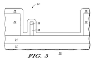
図3は、パッシベーション層20の上、及び開口部24内の絶縁層14及びフィン16(及び、存在する場合はキャップ層18)の上にスペーサ層26が形成された後のデバイス10を示す。スペーサ層26は、例えば堆積プロセスを用いて形成されてもよい。一実施形態において、スペーサ層26は酸化物を含む。スペーサ層26はあらゆる適切な誘電体を含むことができ、そのために誘電性層とも称されることに留意されたい。
FIG. 3 shows the
図4はスペーサ層を異方的にエッチングして、パッシベーション層20の側壁に隣接するスペーサ28、及びフィン16の側壁に隣接するスペーサ30を形成する工程の中間段階におけるデバイス10を示す。図5に示されるように、異方的エッチングはスペーサ30が除去されるまで続けられる。ただし、パッシベーション層20の高さはフィン16の高さよりも高いため、スペーサ28の複数の部分はパッシベーション層20の側壁に隣接したまま残留する。そのため、スペーサ28の高さはパッシベーション層20の高さよりも低いことに留意されたい。後に説明されるように、スペーサ28はデバイス10の機械的特性を向上させるために用いられ得、また、より短いゲート長を得るためにも用いられ得る。(図4及び5において、断面図で示されているために、スペーサ30及び28はそれぞれ別個の部分を含んでいるように見えるが、図8の全体図でスペーサ28に関して示されるように、それらはそれぞれ一つのスペーサの各部分であってもよい点に留意されたい。したがって、各スペーサ28及び30は、それぞれ一つのスペーサ28及び一つのスペーサ30ともみなされ得る。)
図6はパッシベーション層20、スペーサ28、フィン16(及び、存在する場合はキャップ層18)、及び絶縁層14の上のゲート誘電性層32が形成された後のデバイス10を示す。ゲート誘電性層32は、酸化物又は金属酸化物等のあらゆる種類のゲート誘電性材料を含む。ゲート誘電性層32は、例えばハフニウム酸化物等の、二酸化ケイ素よりも高い誘電率(K)を有する材料(よって、高K材料とも称される)を含む。一実施形態において、図6に示されるように、ゲート誘電性層32は化学蒸着(CVD)又は原子層堆積(ALD)によって堆積される。代替の実施形態において、ゲート誘電性層32はフィン16の側壁上に成長させてもよい。この実施形態において、ゲート誘電性層32は、例えば成長させた二酸化ケイ素又は酸窒化ケイ素でもよい。また、この代替の実施形態において、ゲート誘電性層32はフィン16の側壁上のみに成長する。
FIG. 4 shows the
FIG. 6 shows the
次に、ゲート層34がゲート誘電性層32の上に形成される。ゲート層34はあらゆる種類の一つ又は複数のゲート材料を含むことができる。例えば、ゲート層34はシリコンを含んでもよく、又は金属を含んでもよい。さらに、ゲート層34は異なる層を何層含んでもよく、その場合、ゲート層34はゲートスタック層に相当し得る。
A
図7は、ゲート層34を平坦化し、ゲート36を形成した後のデバイス10を示す。ゲート36はゲート電極部分(ゲート電極38)及びゲートコンタクト部分(ゲートコンタクト領域40)を含む。一実施形態において、平坦化の後、ゲート36の頂部はパッシベーション層20の頂部にほぼ連続する。よって、図7は、上述した図8のデバイス10の全体図に沿った水平断面図に相当する点に留意されたい。
FIG. 7 shows the
図9はソース/ドレイン領域44及び46、及びフィン16の中央に沿った断面に相当する断面図を示す。図8のデバイス10の全体図の同じ位置に沿った断面は図10の断面図として示されている。ただし、図9において、パッシベーション層20は依然存在する。したがって、フィン16(及び、存在する場合はキャップ層)の上に重なるゲート36及びスペーサ28が示されている。図9において、ゲート36の下に重なるフィン16の部分はデバイス10のチャネル領域を含む点に留意されたい。また、寸法48はパターン形成されたマスク層22によって画定される開口幅に相当し、デバイス10の実際のゲート長に相当する寸法50よりも大きいことに留意されたい。寸法48はパッシベーション層20の頂部にほぼ連続するゲート36の頂部の長さに相当し、寸法50はスペーサ28に隣接するゲート36の底部の長さに相当する点に留意されたい。そのため、スペーサ28は、パターン形成されたマスク層22又は他のリソグラフィー技術を用いて得られるゲート長よりも短いゲート長を得るために用いられ得る点に留意されたい。
FIG. 9 shows a cross-sectional view corresponding to the cross-section along the center of the source /
図10は図8の全体図に沿った断面図に相当し、パッシベーション層20の除去後のデバイス10を示す。スペーサ28はゲート36の側面に沿って残留する点に留意されたい。したがって、スペーサ28はゲート36に機械的支持を提供し、それによって、現行のフィン型FETデバイスと比較すると、より機械的に安定なデバイスを可能にする。パッシベーション層20の除去後、フィン型FETデバイスを概ね完成させるために従来のプロセスが用いられてもよい。例えば、従来のプロセス技術を用いて、ゲート36の側壁及びスペーサ28に沿ってスペーサが形成されてもよい。また、従来のインプラントを用いて、ソース/ドレイン領域44及び46が形成されてもよい。
10 corresponds to a cross-sectional view along the general view of FIG. 8 and shows the
図11〜16は、本発明の代替の実施形態によって形成され、また、図8のデバイス10をもたらすデバイス10の断面図を示す。図11は、層12、絶縁層14、フィン16、及びキャップ層18を示し、これらは全て図1を参照して説明された。フィン16及びキャップ層18の形成後、パターン形成されたダミーゲート層52がフィン16及びキャップ層18の上に形成される。ダミーゲート層52は後に除去されるため、容易に除去可能な、あらゆる適切な材料から形成される。一実施形態において、ソース/ドレイン注入はダミーゲート層52の形成後に形成されてもよい。この態様において、ダミーゲート層52は注入の間、フィン16を保護し得る。ダミーゲート層52は、後に形成されるゲート電極38の少なくとも一部分のためのダミー構造とみなされてもよい。
FIGS. 11-16 illustrate a cross-sectional view of
図12は、ダミーゲート層52の上にパッシベーション層54が形成された後のデバイス10を示す。パッシベーション層54はパッシベーション層20に類似し、同じプロセス及び材料を用いて形成されてもよい。
FIG. 12 shows the
図13は、パッシベーション層54を平坦化してダミーゲート層52の頂部を露出させた後のデバイス10を示す。図14はダミーゲート層52の除去後のデバイス10を示す。フィン16及びキャップ層18が残留している点に留意されたい。したがって、ダミーゲート層52の除去は、フィン16が位置するパッシベーション層54内の開口部51をもたらす。すなわち、パッシベーション層54内の開口部51は、パッシベーション層54内の空洞の断面である点に留意されたい。開口部51は、上述した開口部24に類似のものである点に留意されたい。ただし、開口部24がゲート電極38及びゲートコンタクト領域44の位置を画定するのに対し、開口部51はフィン16の上に重なるゲートの部分の位置を画定する。
FIG. 13 shows the
図15は、パッシベーション層54の側壁に隣接するスペーサ56の形成を示す。スペーサ56は上述したスペーサ28に類似し、スペーサ28に関して上述したものと同じ方法及び材料を用いて形成されてもよい。例えば、スペーサ層の異方的エッチングを用いてスペーサ56を形成することができ、スペーサ56は酸化物等の誘電性材料を含んでもよい。パッシベーション層20と同様に、パッシベーション層54はフィン16よりも高い高さを有し、フィン16の側壁に隣接するスペーサを形成することなくパッシベーション層54の側壁上にスペーサ56を形成することを可能にしている。また、パッシベーション層54の高さはスペーサ56の高さよりも高い点に留意されたい。(スペーサ30及び28に関して上述したように、断面図で示されるため、スペーサ56は別個の部分を含むように見えるが、一つのスペーサの各部分でもあり得る。したがって、複数のスペーサ56は一つのスペーサ56ともみなされ得る。)
スペーサ56の形成後、ゲート誘電性層58が、パッシベーション層54の上、及び、開口部51内のスペーサ56、絶縁層14、及びフィン16の上に形成される。ゲート誘電性層58の形成後、ゲート層60がゲート誘電性層58の上に形成される。ゲート誘電性層58及びゲート層60は、それぞれ上述したゲート誘電性層32及びゲート層34に類似し、ゲート誘電性層32及びゲート層34に関して上述したものと同じ方法及び材料を用いて形成されてもよい。
FIG. 15 illustrates the formation of
After formation of the
図16は、ゲート層60をパターン形成及びエッチングし、ゲート電極38及びゲートコンタクト領域40を形成した後のデバイス10を示す。上述したゲート36とは異なり、もたらされるゲート60はパッシベーション層54の頂部にほぼ連続しているのではなく、代わりにパッシベーション層54の上に延出し、ゲート電極38の残留部分及びゲートコンタクト領域40を形成している点に留意されたい。よって、ゲート60は図8に示されるように見える点に留意されたい。ただし、スペーサ28に関して図8に示されるように、スペーサ56はゲート電極38及びゲートコンタクト領域40全体の下にではなく、ゲート電極38の一部分の下にのみ重なることに留意されたい。また、図1〜7の実施形態において、ゲートコンタクト領域40を通るフィン16から延出する前記ゲートの部分は、パッシベーション層20がゲート34及び絶縁層14の間に位置していないところの絶縁層14の上に重なることに留意されたい。しかし、図11〜16の実施形態において、パッシベーション層54はほとんど除去されず、ゲート電極38の一部分及びゲートコンタクト領域40はパッシベーション層54の上に形成される点に留意されたい。図1〜7の実施形態のように、スペーサ56は、ゲート長の寸法の減少及び機械的安定性の改善を可能にし得る。
FIG. 16 shows the
本発明は特定の導電型又は電位の極性に関して説明されたが、熟練した技術者は、導電型及び電位の極性が逆転され得ることを理解する。
更に、明細書及び特許請求の範囲において、「正面」、「背面」、「頂部」、「底部」、「上」、「下」等の用語があれば、それらは記述的な目的で用いられており、必ずしも恒常的な位置関係を説明するものではない。ここで説明される本発明の実施形態は、例えばここで示され又は説明される方向以外の他の方向においても実行可能であり、そのような適切な環境下において、上記のように用いられるこれらの用語は、互いに取替えることができるものと理解される。
Although the present invention has been described with respect to a particular conductivity type or polarity of potential, the skilled artisan will understand that the conductivity type and potential polarity can be reversed.
Further, in the specification and claims, if there are terms such as “front”, “back”, “top”, “bottom”, “top”, “bottom”, they are used for descriptive purposes. It does not necessarily explain the permanent positional relationship. The embodiments of the invention described herein can be implemented in other directions than those shown or described herein, for example, and are used as described above in such appropriate environments. Are understood to be interchangeable.
以上の説明において、本発明は特定の実施形態を参照しつつ、詳細に説明されている。しかし、請求項において説明されるように、本発明の範囲から逸脱することなく多様な変形及び変更を実施し得ることを当業者は理解するであろう。したがって、本明細書及び図面は限定的な意味というよりも例示的な意味において認識されるべきであり、そのような変形の全ては本発明の範囲内に含まれるものと意図されている。 In the foregoing description, the invention has been described in detail with reference to specific embodiments. However, one of ordinary skill in the art appreciates that various modifications and changes can be made without departing from the scope of the invention as set forth in the claims. The specification and drawings are, accordingly, to be regarded in an illustrative sense rather than a restrictive sense, and all such variations are intended to be included within the scope of the present invention.
特定の実施形態に関して、利益、他の有利な点、及び問題の解決策が上述されている。しかしながら、これらの利益、有利な点、問題の解決策、及びあらゆる利益、有利な点、解決策を生じさせ又はより顕著にさせ得るあらゆる要素は、本請求項のいずれか若しくは全てにおいて、重要な、必須の、又は不可欠な特徴又は要素として解釈されるものではない。ここで用いられる用語「備える」、「備えている」、又はこれらの用語の他の活用形は、非独占的な包含に及ぶように意図されており、例えば、要素のリストを構成する工程、方法、物品、又は装置はこれらの要素だけを含むのではなく、明示的に記載されていない他の要素や、そのような工程、方法、物品、又は装置に固有の他の要素を含んでもよい。 Benefits, other advantages, and solutions to problems have been described above with regard to specific embodiments. However, these benefits, advantages, solutions to problems, and any factors that may cause or make any benefit, advantage, solution significant, are important in any or all of the claims. It is not to be construed as an essential or essential feature or element. The terms “comprising”, “comprising”, or other uses of these terms, as used herein, are intended to cover non-exclusive inclusions, for example, constructing a list of elements, A method, article, or device does not include only these elements, but may include other elements not explicitly described, or other elements unique to such steps, methods, articles, or devices. .
ここで用いられる「複数」という用語は、2つ又は2つを超えることを意味する。ここで用いられる同用語は別に、少なくとも第2の、又はそれより後順位であることを意味する。 As used herein, the term “plurality” means two or more than two. As used herein, the same term separately means at least second or later.
ここで用いられる「連結された」という用語は、必ずしも直接的に、及び必ずしも機械的にではないが、接続されていることを意味する。
上記の詳細な説明は典型例であるため、「一実施形態」と述べられる場合、それは一つの典型的な実施形態である。したがって、この文脈における「一」という用語の用法は、一つの説明される特徴を有する実施形態が唯一のものであることを示すように意図されているのではない。むしろ、他の多数の実施形態が典型的な「一実施形態」で説明された特徴を有する場合があり、また多くの場合は実際に有する。したがって、上記で用いられたように、本発明が一実施形態の文脈で説明される場合、その一実施形態は本発明の多数の可能な実施形態の中の一つである。
The term “coupled” as used herein means connected, although not necessarily directly and not necessarily mechanically.
Since the above detailed description is exemplary, when "one embodiment" is described, it is one exemplary embodiment. Thus, the usage of the term “one” in this context is not intended to indicate that the embodiment having one described feature is the only one. Rather, many other embodiments may have the features described in the exemplary “one embodiment”, and in many cases actually. Thus, as used above, when the present invention is described in the context of an embodiment, that embodiment is one of many possible embodiments of the present invention.
詳細な説明における「一実施形態」という用語の用法に関する上記の注意書きにかかわらず、当業者は、仮に特定の数の請求項の要素が後続の請求項においても意図される場合、そのような意図はその請求項において明確に記載され、そのような記載がない場合はそのような限定は存在しないか、又は意図されていないことを理解するであろう。例えば、後続の請求項において、ある請求項の要素が「一つ」の特徴を有すると記載される場合、その要素はその説明された特徴の唯一つであると限定されるように意図されている。 Notwithstanding the above remarks regarding the usage of the term “one embodiment” in the detailed description, one of ordinary skill in the art would recognize that if a particular number of claim elements are also intended in subsequent claims, It will be understood that the intention is expressly recited in the claims, and in the absence of such a description, no such limitation exists or is not intended. For example, in a subsequent claim, if an element of a claim is described as having “one” feature, that element is intended to be limited to being the only one of the described features. Yes.
更に、ここで用いられる「一つ」は、一つ又は一つを超えることを意味する。また、特許請求の範囲における「少なくとも一つ」及び「一つ以上」等の前置き句の用法は、たとえ同じ請求項が前置き句の「一つ以上」又は「少なくとも一つ」及び「一つ」等の不定冠詞を含んでいても、不定冠詞の「一つ」による別の請求項の要素の導入が、そのような要素を一つだけ含む発明に対して導入されたそのような請求項の要素を含むいずれかの特定の請求項を限定することを意味すると解釈されてはならない。定冠詞の用法にも同じことが当てはまる。 Further, as used herein, “one” means one or more than one. In addition, the usage of a prefix such as “at least one” and “one or more” in a claim is the same claim as “one or more” or “at least one” and “one”. The introduction of an element of another claim by “one” of the indefinite article, even if such an indefinite article is included, for such a claim introduced to an invention containing only one such element Neither should it be construed as limiting any particular claim containing an element. The same applies to the usage of definite articles.
Claims (5)
半導体層を提供する工程と、
パッシベーション層及びフィンを前記半導体層の上に形成する工程であって、前記パッシベーション層は側壁を有する開口部を備え、前記フィンは前記開口部内に位置し、かつ前記フィンの高さが前記開口部の高さよりも低くなるように、パッシベーション層及びフィンを形成する工程と、
前記開口部内及び前記フィンの上にスペーサ層を堆積する工程と、
前記フィンの側壁に隣接する部分のスペーサ層が除去され、かつ前記開口部の高さよりも低い高さを有するスペーサが前記開口部の側壁に沿って形成されるように、前記スペーサ層を異方的にエッチングする工程と、
前記スペーサの形成後、前記開口部内にゲートの一部分を形成する工程と
からなる方法。 A method of forming a semiconductor device comprising:
Providing a semiconductor layer;
Pas Sshibeshon layer and the fins comprising the steps of forming on the semiconductor layer, wherein the passivation layer includes an opening having a side wall, the fin is located in the opening, and the height of the fins the opening Forming a passivation layer and fins so as to be lower than the height of the part ;
Depositing a spacer layer in the opening and on the fin;
The spacer layer is anisotropically formed so that a portion of the spacer layer adjacent to the side wall of the fin is removed and a spacer having a height lower than the height of the opening is formed along the side wall of the opening. Etching step,
Forming a part of the gate in the opening after forming the spacer;
Rana Ru way or.
前記頂部は前記パッシベーション層の頂部に連続し、かつ第1の寸法を有し、
前記底部は前記スペーサに隣接し、かつ前記スペーサ間に第2の寸法を有し、
前記第2の寸法は前記第1の寸法と平行であり、
前記第1の寸法は前記第2の寸法よりも大きいことからなる請求項1に記載の方法。 Forming a portion of the gate within the opening further comprises forming a portion of the gate such that the portion of the gate has a top and a bottom;
Said top section to continue with the top of the passivation layer, and has a first dimension,
The bottom is adjacent to the spacer and has a second dimension between the spacers;
The second dimension is parallel to the first dimension;
The method of claim 1, wherein the first dimension is greater than the second dimension.
前記スペーサの形成前に前記ダミーゲートを除去する工程とを更に備え、前記ゲートを形成する工程は前記ダミーゲートの除去後に行われるとともに、前記ゲートを形成する工程が、ゲート電極及びゲートコンタクト領域を形成する工程を更に備え、かつ、前記ダミーゲートを形成する工程が、前記ゲート電極のためのダミー構造を形成する工程を更に備える請求項1に記載の方法。 Forming a dummy gate on the fin;
Removing the dummy gate before forming the spacer, and the step of forming the gate is performed after the removal of the dummy gate, and the step of forming the gate includes the gate electrode and the gate contact region. The method of claim 1, further comprising forming and forming the dummy gate further comprises forming a dummy structure for the gate electrode.
Applications Claiming Priority (3)
| Application Number | Priority Date | Filing Date | Title |
|---|---|---|---|
| US11/380,530 | 2006-04-27 | ||
| US11/380,530 US7442590B2 (en) | 2006-04-27 | 2006-04-27 | Method for forming a semiconductor device having a fin and structure thereof |
| PCT/US2007/063966 WO2007127533A2 (en) | 2006-04-27 | 2007-03-14 | Method for forming a semiconductor device having a fin and structure thereof |
Publications (3)
| Publication Number | Publication Date |
|---|---|
| JP2009535820A JP2009535820A (en) | 2009-10-01 |
| JP2009535820A5 JP2009535820A5 (en) | 2010-04-30 |
| JP5208918B2 true JP5208918B2 (en) | 2013-06-12 |
Family
ID=38648827
Family Applications (1)
| Application Number | Title | Priority Date | Filing Date |
|---|---|---|---|
| JP2009507865A Active JP5208918B2 (en) | 2006-04-27 | 2007-03-14 | Method for forming a semiconductor device having fins |
Country Status (6)
| Country | Link |
|---|---|
| US (1) | US7442590B2 (en) |
| JP (1) | JP5208918B2 (en) |
| KR (1) | KR20090005066A (en) |
| CN (1) | CN101432877B (en) |
| TW (1) | TWI404206B (en) |
| WO (1) | WO2007127533A2 (en) |
Cited By (1)
| Publication number | Priority date | Publication date | Assignee | Title |
|---|---|---|---|---|
| US9283273B2 (en) | 1995-07-27 | 2016-03-15 | Genentech, Inc. | Protein formulation |
Families Citing this family (12)
| Publication number | Priority date | Publication date | Assignee | Title |
|---|---|---|---|---|
| US8202780B2 (en) * | 2009-07-31 | 2012-06-19 | International Business Machines Corporation | Method for manufacturing a FinFET device comprising a mask to define a gate perimeter and another mask to define fin regions |
| US8901665B2 (en) * | 2011-12-22 | 2014-12-02 | Taiwan Semiconductor Manufacturing Company, Ltd. | Gate structure for semiconductor device |
| US8987823B2 (en) | 2012-11-07 | 2015-03-24 | International Business Machines Corporation | Method and structure for forming a localized SOI finFET |
| US8766363B2 (en) | 2012-11-07 | 2014-07-01 | International Business Machines Corporation | Method and structure for forming a localized SOI finFET |
| US20140167162A1 (en) | 2012-12-13 | 2014-06-19 | International Business Machines Corporation | Finfet with merge-free fins |
| US8981496B2 (en) | 2013-02-27 | 2015-03-17 | Taiwan Semiconductor Manufacturing Company, Ltd. | Metal gate and gate contact structure for FinFET |
| US9018054B2 (en) | 2013-03-15 | 2015-04-28 | Applied Materials, Inc. | Metal gate structures for field effect transistors and method of fabrication |
| US8969155B2 (en) | 2013-05-10 | 2015-03-03 | International Business Machines Corporation | Fin structure with varying isolation thickness |
| US9287372B2 (en) * | 2013-12-27 | 2016-03-15 | Taiwan Semiconductor Manufacturing Company Limited | Method of forming trench on FinFET and FinFET thereof |
| US9679985B1 (en) * | 2016-06-20 | 2017-06-13 | Globalfoundries Inc. | Devices and methods of improving device performance through gate cut last process |
| CN109427664B (en) * | 2017-08-24 | 2021-08-06 | 中芯国际集成电路制造(上海)有限公司 | Semiconductor structure and forming method thereof |
| US11973143B2 (en) | 2019-03-28 | 2024-04-30 | Intel Corporation | Source or drain structures for germanium N-channel devices |
Family Cites Families (9)
| Publication number | Priority date | Publication date | Assignee | Title |
|---|---|---|---|---|
| JP4044276B2 (en) * | 2000-09-28 | 2008-02-06 | 株式会社東芝 | Semiconductor device and manufacturing method thereof |
| US6800905B2 (en) * | 2001-12-14 | 2004-10-05 | International Business Machines Corporation | Implanted asymmetric doped polysilicon gate FinFET |
| US6803631B2 (en) * | 2003-01-23 | 2004-10-12 | Advanced Micro Devices, Inc. | Strained channel finfet |
| US6855582B1 (en) * | 2003-06-12 | 2005-02-15 | Advanced Micro Devices, Inc. | FinFET gate formation using reverse trim and oxide polish |
| US6855989B1 (en) * | 2003-10-01 | 2005-02-15 | Advanced Micro Devices, Inc. | Damascene finfet gate with selective metal interdiffusion |
| US6951783B2 (en) | 2003-10-28 | 2005-10-04 | Freescale Semiconductor, Inc. | Confined spacers for double gate transistor semiconductor fabrication process |
| US6936516B1 (en) | 2004-01-12 | 2005-08-30 | Advanced Micro Devices, Inc. | Replacement gate strained silicon finFET process |
| US7041542B2 (en) * | 2004-01-12 | 2006-05-09 | Advanced Micro Devices, Inc. | Damascene tri-gate FinFET |
| JP4796329B2 (en) * | 2004-05-25 | 2011-10-19 | 三星電子株式会社 | Manufacturing method of multi-bridge channel type MOS transistor |
-
2006
- 2006-04-27 US US11/380,530 patent/US7442590B2/en active Active
-
2007
- 2007-03-14 KR KR1020087026162A patent/KR20090005066A/en not_active Application Discontinuation
- 2007-03-14 WO PCT/US2007/063966 patent/WO2007127533A2/en active Application Filing
- 2007-03-14 CN CN200780015277XA patent/CN101432877B/en active Active
- 2007-03-14 JP JP2009507865A patent/JP5208918B2/en active Active
- 2007-03-22 TW TW096109944A patent/TWI404206B/en active
Cited By (1)
| Publication number | Priority date | Publication date | Assignee | Title |
|---|---|---|---|---|
| US9283273B2 (en) | 1995-07-27 | 2016-03-15 | Genentech, Inc. | Protein formulation |
Also Published As
| Publication number | Publication date |
|---|---|
| WO2007127533A3 (en) | 2008-06-26 |
| WO2007127533A2 (en) | 2007-11-08 |
| JP2009535820A (en) | 2009-10-01 |
| TW200742070A (en) | 2007-11-01 |
| US7442590B2 (en) | 2008-10-28 |
| CN101432877A (en) | 2009-05-13 |
| KR20090005066A (en) | 2009-01-12 |
| CN101432877B (en) | 2011-09-28 |
| TWI404206B (en) | 2013-08-01 |
| US20070254435A1 (en) | 2007-11-01 |
Similar Documents
| Publication | Publication Date | Title |
|---|---|---|
| JP5208918B2 (en) | Method for forming a semiconductor device having fins | |
| US7629220B2 (en) | Method for forming a semiconductor device and structure thereof | |
| US9859375B2 (en) | Stacked planar double-gate lamellar field-effect transistor | |
| US8637384B2 (en) | FinFET parasitic capacitance reduction using air gap | |
| JP5409997B2 (en) | Method for forming a gate in a FinFET device and method for manufacturing a semiconductor device | |
| US9472407B2 (en) | Replacement metal gate FinFET | |
| KR101369134B1 (en) | Nanowire mesh device and method of fabricating same | |
| US10170634B2 (en) | Wire-last gate-all-around nanowire FET | |
| US8742508B2 (en) | Three dimensional FET devices having different device widths | |
| US9123654B2 (en) | Trilayer SIT process with transfer layer for FINFET patterning | |
| US9214529B2 (en) | Fin Fet device with independent control gate | |
| US9634125B2 (en) | Fin field effect transistor device and fabrication method thereof | |
| US8053348B2 (en) | Method of forming a semiconductor device using a sacrificial uniform vertical thickness spacer structure | |
| US20160049467A1 (en) | Fin field effect transistor device and fabrication method thereof | |
| US20140084371A1 (en) | Multi-gate field effect transistor devices | |
| WO2013029314A1 (en) | Semiconductor device and manufacturing method thereof | |
| TWI502649B (en) | Method of fabricating double-gate and tri-gate transistors on common substrate | |
| TW202105617A (en) | A method for forming a semiconductor device |
Legal Events
| Date | Code | Title | Description |
|---|---|---|---|
| A521 | Request for written amendment filed |
Free format text: JAPANESE INTERMEDIATE CODE: A523 Effective date: 20100310 |
|
| A621 | Written request for application examination |
Free format text: JAPANESE INTERMEDIATE CODE: A621 Effective date: 20100310 |
|
| RD04 | Notification of resignation of power of attorney |
Free format text: JAPANESE INTERMEDIATE CODE: A7424 Effective date: 20120228 |
|
| A131 | Notification of reasons for refusal |
Free format text: JAPANESE INTERMEDIATE CODE: A131 Effective date: 20120918 |
|
| A521 | Request for written amendment filed |
Free format text: JAPANESE INTERMEDIATE CODE: A523 Effective date: 20121217 |
|
| TRDD | Decision of grant or rejection written | ||
| A01 | Written decision to grant a patent or to grant a registration (utility model) |
Free format text: JAPANESE INTERMEDIATE CODE: A01 Effective date: 20130129 |
|
| A61 | First payment of annual fees (during grant procedure) |
Free format text: JAPANESE INTERMEDIATE CODE: A61 Effective date: 20130220 |
|
| FPAY | Renewal fee payment (event date is renewal date of database) |
Free format text: PAYMENT UNTIL: 20160301 Year of fee payment: 3 |
|
| R150 | Certificate of patent or registration of utility model |
Ref document number: 5208918 Country of ref document: JP Free format text: JAPANESE INTERMEDIATE CODE: R150 Free format text: JAPANESE INTERMEDIATE CODE: R150 |
|
| R250 | Receipt of annual fees |
Free format text: JAPANESE INTERMEDIATE CODE: R250 |
|
| R250 | Receipt of annual fees |
Free format text: JAPANESE INTERMEDIATE CODE: R250 |
|
| S533 | Written request for registration of change of name |
Free format text: JAPANESE INTERMEDIATE CODE: R313533 |
|
| R350 | Written notification of registration of transfer |
Free format text: JAPANESE INTERMEDIATE CODE: R350 |
|
| R250 | Receipt of annual fees |
Free format text: JAPANESE INTERMEDIATE CODE: R250 |
|
| R250 | Receipt of annual fees |
Free format text: JAPANESE INTERMEDIATE CODE: R250 |
|
| R250 | Receipt of annual fees |
Free format text: JAPANESE INTERMEDIATE CODE: R250 |
|
| R250 | Receipt of annual fees |
Free format text: JAPANESE INTERMEDIATE CODE: R250 |
|
| R250 | Receipt of annual fees |
Free format text: JAPANESE INTERMEDIATE CODE: R250 |
|
| R250 | Receipt of annual fees |
Free format text: JAPANESE INTERMEDIATE CODE: R250 |
|
| R250 | Receipt of annual fees |
Free format text: JAPANESE INTERMEDIATE CODE: R250 |