JP5203102B2 - Operation method of semiconductor processing equipment - Google Patents
Operation method of semiconductor processing equipment Download PDFInfo
- Publication number
- JP5203102B2 JP5203102B2 JP2008223882A JP2008223882A JP5203102B2 JP 5203102 B2 JP5203102 B2 JP 5203102B2 JP 2008223882 A JP2008223882 A JP 2008223882A JP 2008223882 A JP2008223882 A JP 2008223882A JP 5203102 B2 JP5203102 B2 JP 5203102B2
- Authority
- JP
- Japan
- Prior art keywords
- wafer
- vacuum
- vacuum robot
- axis sensor
- chamber
- Prior art date
- Legal status (The legal status is an assumption and is not a legal conclusion. Google has not performed a legal analysis and makes no representation as to the accuracy of the status listed.)
- Active
Links
Images


Description
本発明は、半導体処理装置の処理室等の間で、半導体被処理基板(以下、「ウエハ」という。)を移動させることに関し、更に詳細には、ウエハの位置を補正する真空処理方法及び真空搬送装置に関する。 The present invention relates to moving a semiconductor substrate to be processed (hereinafter referred to as “wafer”) between processing chambers of a semiconductor processing apparatus, and more specifically, a vacuum processing method and a vacuum for correcting the position of a wafer. The present invention relates to a transport device.
半導体デバイスの製造では、処理室等を相互に接続させて、接続された処理室等の間で、ウエハを移送できるようにすることが望ましい。このような移送は、真空搬送室であるバッファ室や処理室を構成する真空容器の側壁の内部を連通する通路を通してこれら内部の室間でウエハを移送する真空搬送装置によって行われる。真空搬送装置は、一般に、半導体エッチングシステム、材料堆積システム、フラットパネルディスプレイエッチングシステムを含む、種々のウエハ処理モジュールと連携して使用される。 In the manufacture of semiconductor devices, it is desirable to connect processing chambers and the like so that wafers can be transferred between the connected processing chambers. Such transfer is performed by a vacuum transfer device that transfers wafers between the chambers through a passage communicating with the inside of the side walls of the vacuum chamber constituting the buffer chamber and the processing chamber, which are vacuum transfer chambers. Vacuum transfer devices are typically used in conjunction with various wafer processing modules, including semiconductor etching systems, material deposition systems, and flat panel display etching systems.
真空処理における清浄度および高処理精度への要求が増すにつれて、処理工程中および処理工程間を真空条件下で連続して行うため真空搬送装置が採用されている。真空搬送装置は、例えば、ウエハが授受されるポートや容器とウエハが実際に処理される処理室、例えば、その表面をエッチングされたり膜を堆積させたりする複数の処理室との間に設置される。そして、真空搬送装置内に設置されたロボットアームを利用して、これら容器と処理室との間でウエハを搬送してやり取りすることができるように構成されている。 As demands for cleanliness and high processing accuracy in vacuum processing increase, a vacuum transfer device is employed to continuously perform processing steps and between processing steps under vacuum conditions. The vacuum transfer device is installed between, for example, a port through which a wafer is transferred and a container and a processing chamber in which the wafer is actually processed, for example, a plurality of processing chambers in which the surface is etched or a film is deposited. The A wafer can be transferred and exchanged between these containers and the processing chamber using a robot arm installed in the vacuum transfer device.
一方、このようなロボットの使用において、ウエハを移送するにあたって幾つかの問題が生じていた。例えば、ウエハをロードロック室等の一方の室から目的箇所である別の処理室等他方の室内へ移送する場合に、目的箇所の所望の位置にウエハが適切に設置または位置決めされない問題が生じる虞がある。例えば、特許文献1には、ウエハの中心が適切に設置または位置決めされない場合に、ウエハの位置補正を行うシステムとして、R軸方向にセンサを設けて検出する方式が記載されている。
しかしながら、上記の従来技術であるウエハの位置補正のシステムでは、以下の問題点があった。
(1)補正量Sθ、補正量SRが規格値を外れた場合、補正動作を行うようにしているが、この補正量Sθ、補正量SRには規格値しかないため、規格値を外れた全ての補正量に対して補正動作を行う。したがって、センサ出力不良等による想定外の補正量に対しても補正動作を行うことになる。
(2)ウエハ位置ずれエラーの場合は、事前の警告もなしに装置が停止する。
(3)補正動作後のセンサ出力データをクリアしないため、補正動作後に真空ロボットの収縮動作を行い、そのまま伸張させると、前回動作時のθ軸センサ出力と本伸張時のR軸センサ出力値で計算を行うため、実際の真空ロボットに対する位置データとは異なる計算結果となる。
(4)計算に使用するセンサの出力が複数回ある等のセンサ異常の場合でも、補正計算を行う。
However, the above-described prior art wafer position correction system has the following problems.
(1) When the correction amount Sθ and the correction amount SR deviate from the standard value, the correction operation is performed. However, since the correction amount Sθ and the correction amount SR have only the standard value, all the values out of the standard value are used. The correction operation is performed for the correction amount. Therefore, a correction operation is performed even for an unexpected correction amount due to a sensor output defect or the like.
(2) In the case of a wafer misalignment error, the apparatus stops without any prior warning.
(3) Since the sensor output data after the correction operation is not cleared, if the contraction operation of the vacuum robot is performed after the correction operation and is expanded as it is, the θ-axis sensor output during the previous operation and the R-axis sensor output value during the main expansion are used. Since the calculation is performed, the calculation result is different from the position data for the actual vacuum robot.
(4) The correction calculation is performed even in the case of a sensor abnormality such as a plurality of sensor outputs used for the calculation.
本発明の目的は、センサ出力不良等による想定外の補正量、また真空ロボットに対する位置データの誤計算に対しても適切に処置することができ、スループットの高い真空処理装置または真空処理方法を提供することにある。 An object of the present invention is to provide a high-throughput vacuum processing apparatus or vacuum processing method capable of appropriately taking measures against unexpected correction amounts due to sensor output defects and the like, and miscalculation of position data for a vacuum robot. There is to do.
上記の目的を達成するため、本発明の真空処理装置の運転方法は、真空搬送室であるバッファ室の内部に配置された真空ロボットによりウエハを上記バッファ室に連結された複数の真空容器のうちの少なくとも1つに搬送し、上記真空容器の内部に配置された試料台上に上記ウエハを載置して処理する真空処理方法であって、上記真空ロボットによる上記ウエハの前記真空容器の1つへの搬送中において、上記真空ロボットの回転時に上記ウエハの遮光角度を検出するθ軸センサと、上記真空ロボットの伸縮時に上記ウエハの遮光距離を検出するR軸センサとの出力に基づいて、上記ウエハの上記真空ロボットに対する位置補正量を求め、上記位置補正量が所定の値の範囲を超えた場合には、上記真空ロボットの搬送の動作停止を行い、動作停止後は、上記バッファ室に連結され上記真空ロボット上の上記ウエハの位置を外部から確認可能な室に搬送されて上記位置が確認された上記ウエハを上記真空容器の1つへ再度搬送するリトライ動作を行うことを特徴とする。 In order to achieve the above object, a method of operating a vacuum processing apparatus according to the present invention includes: a plurality of vacuum containers in which a wafer is connected to the buffer chamber by a vacuum robot disposed inside a buffer chamber that is a vacuum transfer chamber. A vacuum processing method in which the wafer is placed and processed on a sample stage disposed inside the vacuum container, wherein one of the vacuum containers of the wafer by the vacuum robot is provided. Based on the outputs of the θ-axis sensor that detects the light shielding angle of the wafer when the vacuum robot rotates and the R-axis sensor that detects the light shielding distance of the wafer when the vacuum robot expands and contracts. obtain the position correction amount for the vacuum robot wafer, when the position correction amount is out of the range of predetermined value, performs an operation stop of the conveyance of the vacuum robot operation Stop after the retry for transporting the wafer is conveyed to the ascertainable chambers above position was confirmed the position of the wafer on the concatenated the vacuum robot in the buffer chamber from the outside again to one of the vacuum vessel It is characterized by performing an operation.
本発明によれば、θ軸センサ及びR軸センサの出力に基づいて、ウエハの真空ロボットに対する回転方向の補正量と直進方向の補正量を求めて、これらが所定の規格値を外れていた場合に位置データの変更動作を行い、許容値を超えていれば補正量範囲オーバーエラーとして動作を停止することができ、かつ補正量範囲オーバーエラー時はウエハクリアにて補正動作のリトライを行うこともできる。また、上記θ軸センサ及び上記R軸センサの出力に基づいて得られた距離データの差が規格値を越えていた場合には、位置ずれエラーとして警告を発信することで、ウエハ保持力低下の警告およびしても適切に対処することができる。 According to the present invention, based on the outputs of the θ-axis sensor and the R-axis sensor, the correction amount in the rotation direction and the correction amount in the straight direction of the wafer with respect to the vacuum robot are obtained, and these are out of a predetermined standard value. If the value exceeds the allowable value, the operation can be stopped as a correction amount range over error, and if the correction amount range over error occurs, the correction operation can be retried by clearing the wafer. it can. Further, when the difference in distance data obtained based on the outputs of the θ-axis sensor and the R-axis sensor exceeds a standard value, a warning is issued as a misalignment error, thereby reducing the wafer holding power. Warnings and even appropriate actions can be taken.
以下、本発明の実施の形態について、図面を用いて詳細に説明する。 Hereinafter, embodiments of the present invention will be described in detail with reference to the drawings.
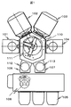
図1は、本発明の実施例である半導体処理装置100の全体構成図を示している。半導体処理装置100は、複数(4個)の処理室101,102,103,104と、複数(3個)のカセット設置台105との間でウエハを移送することができる。
FIG. 1 shows an overall configuration diagram of a semiconductor processing apparatus 100 according to an embodiment of the present invention. The semiconductor processing apparatus 100 can transfer wafers between a plurality (four) of
処理室101,102,103,104は、プラズマエッチング、層の堆積、および/またはスパッタリングを実行するための処理室であっても良い。これら処理室101,102,103,104は、所定の圧力(真空圧)に減圧される内部の空間にウエハ等試料が載置される試料台を有した真空処理容器から構成され、その内部の空間に処理用のガスを供給しつつ図示しない電界または磁界の供給手段から電界または磁界を印加して処理室のウエハ上方の空間にプラズマを形成し、試料の表面を処理する処理容器となっている。
The
真空処理装置である半導体処理装置100のバッファ室110は、内部が前記処理室101等の内部と同等の圧力に調節可能な真空容器から構成され、ウエハを真空側に導入するために実装された複数のロードロック室106,107が接続されている。なお、処理室101,102,103,104、バッファ室110、ロードロック室106,107は、減圧された条件で試料を搬送、処理を行う真空側ブロックを構成している。
The
複数のロードロック室106,107は、大気ロボット108が内部の空間に配置された大気搬送室109に接続され、この大気搬送室109は、ウエハが収納されるカセットがその上面に載置されるカセット載置台105を前面側に備えている。ロードロック室106,107は、カセットが連結される大気搬送室109と真空側ブロックとの間でのウエハの取り出しや受け渡しのための開閉機構であるとともに、可変圧インタフェースとして機能する。
The plurality of
大気ロボット108は、戴置されるカセット戴置台105に戴置されたカセットからウエハを取り出して、大気搬送室109に運び、大気搬送室109内でウエハのセンタリング及びノッチ合わせを行った後、再び、ロードロック室106または107に搬入する。
The
ロードドック室または107に搬入されたウエハは、その内側に配置された試料台上に載置される。内部が減圧された後、試料台内に配置された複数のピン形状のウエハプッシャーに持ち上げられた状態で真空ロボット111のアーム先端部のハンドがウエハ下方に移動してそのハンド上へウエハの受渡しが行われる。ウエハの受渡しが完了すると真空ロボット111のアームが縮み、ハンド上に載せられたウエハがバッファ室110内に運び込まれる。
The wafer carried into the load dock chamber or 107 is placed on a sample stage disposed inside the load dock chamber or 107. After the inside is depressurized, the hand at the tip of the arm of the
バッファ室110内で、真空ロボット111の回転動作により、処理室101,102,103,104の方向に向きが変更され、真空ロボット111のアームの伸張動作により、ウエハが、処理室101,102,103,104に移送されて、処理室内で、プラズマエッチング、層の堆積、および/またはスパッタリングなどの処理が実行される。
In the
これらの処理は密封された処理室内で行われる。例えば、処理室101の内側に搬送されたウエハは、図示しない試料台上に載置される。この際、ロードロック室106または107内側の構成と同様に、試料台内部に配置された上下に移動してウエハを上下に昇降させる複数のプッシャピンを備えている。
These processes are performed in a sealed processing chamber. For example, the wafer transferred to the inside of the
これらのプッシャピンが上方に移動した状態で、その上方に位置する真空ロボット111のアーム先端側のハンド上に載せられたウエハがアームの下降に伴ってプッシャピン上に載せられた後、アームがバッファ室110内に移動してウエハの試料台への受渡しが行われる。アームの移動後に、プッシャピンは下方に移動され試料台内に格納されて、ウエハが試料台上の上面の誘電体製膜に被覆されたウエハ載置面上に載せられる。
With these pusher pins moving upward, a wafer placed on the arm tip side hand of the
その後、処理室101内に処理用ガスが導入されると共に、処理室101内は図示しない真空ポンプの動作により排気されて所定の圧力(真空圧)に調節される。また、誘電体製膜内に配置された静電吸着用の電極に電力が印加されることで生起されるウエハと誘電体製膜との間の静電吸着力により、試料台上のウエハ載置面上にウエハが吸着、保持される。
Thereafter, a processing gas is introduced into the
さらに、ウエハ載置面の表面とウエハ裏面との間には、He等の熱伝達用のガスが導入されて、ウエハと試料台との間の熱伝達が調節されてウエハの表面の温度が所望の範囲に調節される。この状態で、処理室101内のウエハ上方の空間に電界または磁界が供給されて処理用ガスがプラズマ化され、このプラズマを用いてウエハ表面が処理される。
In addition, a heat transfer gas such as He is introduced between the front surface of the wafer mounting surface and the back surface of the wafer, and the heat transfer between the wafer and the sample table is adjusted so that the temperature of the front surface of the wafer is increased. Adjust to the desired range. In this state, an electric field or a magnetic field is supplied to the space above the wafer in the
この処理の終了後に、静電吸着電極に印加された電力が除かれて静電吸着力が低減された後、プッシャピンを上昇させてウエハがウエハ載置面から上方に持ち上げられる。処理室101の密封しているゲートバルブが開放された後、真空ロボット111のアームが伸張されて先端側のハンドがウエハの下方に位置するように移動される。プッシャピンの下方の移動によって、ウエハがハンド上の保持面上に載せられてアームに受け渡される。プッシャピンはその後、再び試料台内部に格納される。
After this process is completed, the power applied to the electrostatic chucking electrode is removed to reduce the electrostatic chucking force, and then the pusher pin is raised to lift the wafer upward from the wafer mounting surface. After the gate valve sealed in the
このように、処理室101,102,103,104内での処理の実行後、処理済のウエハが真空ロボット111に受け渡され、真空ロボット111のアームの収縮動作、真空ロボット111の回転動作、真空ロボット111のアームの伸張動作の組合せにより、ウエハが処理室同士または処理室とロードロック室との間を移送される。
As described above, after the processing in the
上記真空ロボット111または大気ロボット108の動作は、図示しない各々用の制御装置により調節される。このような制御装置は、真空処理装置100全体の動作を制御する制御装置と指令を授受可能に接続されるか、またはこれと一体となっていても良い。
The operation of the
このような真空ロボット111によるウエハの受け渡しまたは搬送の際には、例え動作が制御された真空ロボット111あるいはそのアーム上に載せられたウエハは、所期の位置から距離が離れてズレた位置に保持される場合が有り、このため、搬送先の目的の位置に精密に位置決めして載置できなくなる虞が有る。
When the wafer is transferred or transferred by the
すなわち、ウエハの受渡しの際に、ウエハとアームまたはこの先端側のハンド上の所定の位置との間にズレが生じたり、搬送中にウエハがアームまたはハンド上で位置が移動したりする問題が生じる。例えば、ウエハがプッシャピンにより持ち上げられて真空ロボット111のアームがその動作を制御されてウエハ下方の所定の位置にアーム先端側のハンドが配置されたとしても、ウエハがプッシャピンで持ち上げられたその位置がアームまたはハンドにウエハを載せる際の基準となる位置と異なっている場合には、上記ズレが生じてしまう。これは、ウエハを持ち上げる際に静電吸着力が特定の大きさ以上残っていたり、プッシャピンの配置や形状、位置の不均等があると生起しやすい。また、ウエハのウエハ載置面上に載置された状態でその載置の基準となる位置からズレている場合にも、受渡しでの基準位置からのズレが生じてしまう。
In other words, there is a problem that when the wafer is delivered, there is a gap between the wafer and a predetermined position on the arm or the hand on the tip side, or the position of the wafer moves on the arm or the hand during transfer. Arise. For example, even if the wafer is lifted by the pusher pin and the arm of the
このようなウエハの位置の変動があると、処理室内の試料台等の目的箇所でのウエハ載置面へのウエハの位置決めが不安定となり、ウエハを保持する吸着力のウエハ面上で不均一や処理の不均一を生起して処理の歩留まりを低下させてしまう。また、ウエハの受渡しの際に安定してアームまたはハンド上に載置できず搬送中にウエハが落下したり装置内部の表面と接触したりして事故や汚染が生起するという問題が生じていた。このため、ウエハをアームまたはハンドの上面や試料台上の載置面の目的の位置に精度良く載置すること、または受渡しすることが求められている。 If there is such a variation in the position of the wafer, the positioning of the wafer with respect to the wafer mounting surface at a target location such as a sample stage in the processing chamber becomes unstable, and the suction force for holding the wafer is not uniform on the wafer surface. Or non-uniformity of processing, and the processing yield is reduced. In addition, there was a problem that the wafer could not be stably placed on the arm or hand when the wafer was delivered, and the wafer dropped during transportation or contacted with the surface inside the apparatus, resulting in an accident or contamination. . For this reason, it is required to accurately place or deliver the wafer to a target position on the upper surface of the arm or hand or the placement surface on the sample table.
さらに、ウエハを搬送する際の真空ロボット111の動作により、アームの上面でウエハがその位置を移動してしまう場合がある。これを抑制しようとして、ウエハの外形や径に合わせてその外終縁と接してウエハを保持するピンをアーム上に配置して、ウエハの位置を固定することが考えられる。しかし、この場合、アームの位置を高精度に制御しなければウエハ外周縁を複数ピンで接触または支持できないため、適正な支持ができずウエハが落下したり傾いて搬送されたりして目的箇所に適正に載置できないという事故が増大して却って処理の効率を低下させてしまう。或いは、真空ロボット111のコストが増大して装置全体の製造コストが増大するという問題が生起する。或いはまた、ピンとウエハ外周端縁との接触により塵埃が生起して異物となってウエハや処理室等の装置内を汚染して処理の歩留まりが低下したり、クリーニングの頻度を増大させて処理効率が低下してしまう。
Further, the operation of the
このため、本実施例では、ウエハの裏面をアーム先端側のハンド上の面または複数の点で支持するとともにウエハ外周縁の周囲に隙間をあけてこれを保持する技術が採用される。
本実施例の構成では、真空ロボット111の停止や移動によって、ウエハの搬送中のウエハの位置の移動が生じる虞が有る場合に、生じたウエハの位置の移動(ズレ)を検出し、これに対応して真空処理装置の搬送や処理の動作を調節する。
For this reason, in this embodiment, a technique is adopted in which the back surface of the wafer is supported by a surface or a plurality of points on the hand on the tip side of the arm and a gap is formed around the outer periphery of the wafer.
In the configuration of this embodiment, when there is a possibility that the movement of the wafer position during the wafer transfer may occur due to the stop or movement of the
図2は、半導体処理装置100の真空搬送装置200(バッファ室110)内のセンサ取り付け位置を示している。真空搬送装置200には、これを構成する真空容器の側面に複数個の処理室101,102,103,104と複数個のロードロック室106,107が連結され、これら内部を連通する通路を介してこれら処理室とロードロック室との間でウエハの移送が可能となっている。
FIG. 2 shows a sensor mounting position in the vacuum transfer device 200 (buffer chamber 110) of the semiconductor processing apparatus 100. A plurality of
本実施例では、真空ロボット111は、バッファ室110の中央近傍にその中心203が配置され、この中心203を軸として所定の角度θの回転が可能となっている。この中心203を中心軸とした真空ロボット111またはそのアームの回転動作をθ軸の動作またはθ軸(周り)の回転という。
In the present embodiment, the
さらに、真空ロボット111は、所定のθ軸の回転角度位置で、そのアームを中心203側とバッファ室110の外周側(処理室側)とを結ぶ方向に伸縮可能してその先端部のウエハ載置用のハンドの位置をバッファ室110内と処理室内とを往き、戻りの移動をさせることが可能となっている。この伸縮の動作をR軸(方向)の動作という。
Furthermore, the
本発明では、半導体処理装置100の真空搬送装置200(バッファ室110)内に、真空ロボット111の動作方向であるθ軸及びR軸のそれぞれに。θ軸センサ201、R軸センサ202を設けている。(ロードロック室2室、処理室4室の装置構成の場合は、θ軸用が6ケ、R軸用が6ケとなる。)
θ軸センサ201は、真空ロボット111の中心203を中心とした円周上に、複数個(少なくとも処理室およびロードロック室の個数)配置され、本実施例では、バッファ室110の上下各々に配置された1対を1個とする指向性の高い光センサであって上下の一方から他方へ向かう光の量を検出するセンサであり、上下のセンサの取り付け位置でのセンサ対の間のウエハの有無あるいはその通過がウエハの遮光によって検出されるものである。このような対のセンサを真空ロボット111の回転動作時にウエハがその間を通過する半径位置に配置することで、真空ロボット111の回転時のθ軸センサ201の出力を用いて、真空ロボット中心からウエハ中心までの距離を算出することができる。
In the present invention, in the vacuum transfer apparatus 200 (buffer chamber 110) of the semiconductor processing apparatus 100, each of the θ axis and the R axis, which are the operation directions of the
A plurality of θ-axis sensors 201 (at least the number of processing chambers and load lock chambers) are arranged on the circumference centered on the
また、R軸センサ202は、真空ロボット111のアームの伸縮方向、即ち、各処理室あるいはロードロック室と中心203とを結ぶ方向に沿った線上に配置され、本実施例ではθ軸センサ201と同様に指向性の高い光センサであって、ウエハが載せられたアームの伸張動作の際のウエハの遮光によってそのセンサの取り付け位置での通過あるいはウエハの有無が検出される。本実施例ではθ軸センサ201と同様に指向性の高い光センサであって、ウエハが載せられたアームの伸張動作の際のウエハの遮光によってそのセンサの取り付け位置での通過あるいはウエハの有無が検出される。アームの伸縮時のR軸センサ202の出力を用いて、真空ロボット111のハンド中心とウエハ中心との距離を算出することができる。
The R-
上記θ軸センサ201、R軸センサ202は、後述するウエハが処理室退避位置、あるいは待機位置にある場合に、ウエハがこれらの対の間に位置して有無が検出されない位置に配置されている。すなわち、本実施例では上記θ軸センサ201、R軸センサ202はウエハの通過とその時刻を検出するためのものであり、ウエハの有無を検出するものではない。
The θ-
これらのθ軸センサ201、R軸センサ202から求められる変位量を計算し、所定の規格値以上の変位量がある場合に限り位置の補正を行なう。尚、この変位量の求め方は、ティーチング時の値を絶対値とし、それからの差分にて変位量を求めるものである。
The displacement amount obtained from the θ-
ティーチングは、大気ロボット108側と真空ロボット111側とでそれぞれ行なわれる。真空ロボット111側で行なうのは、真空ロボット111の動作原点から各処理室までの回転角度と、搬入前の退避位置から各処理室間までの距離のあわせ込みである。つまり、アームまたはハンドの位置を可動の範囲内で自由に調節可能な真空ロボット111あるいはその制御装置に対して、その動作の基準となる位置をその上に載せられるウエハの特定の位置または処理室101内部の試料台等の装置内の目的箇所の特定の位置に対する相対的な位置の情報として記憶させ、設定するものである。
Teaching is performed on the
例えば、アームのハンド上の特定の位置に載せられたウエハの特定位置と処理室101の試料台上の特定位置とが所定の距離に配置されるアームの位置を基準となる位置の情報として設定する。このような基準の位置の情報に基づいて真空ロボット111のθ軸方向の回転やR軸方向の伸縮の動作によるアームの位置が調節される。尚、これら調整は、ハンド中心と各処理室の中心が合致するように治具を用いて行う。
For example, the position of the arm where the specific position of the wafer placed at a specific position on the hand of the arm and the specific position on the sample stage in the
図3には、上記ティーチングにおけるθ軸センサ201を用いた真空ロボット111またはウエハの位置の情報を検出する要領を模式的に示している。
FIG. 3 schematically shows a procedure for detecting information on the position of the
遮光角度θ1は、θ軸センサ201のON−OFFを読み取ることで、
θ1=θon−θoff(deg)・・・(1)
により求められ、この求められたθ1より、距離Aは、
A=cos(θ1/2)×L1(mm)・・・(2)
となる。
また、θ軸センサ201の取り付け距離Llと求められた距離Aより、距離Bは、
B=√(L12−A2)(mm)・・・(3)
となる。
また、ウエハ半径rと、求められた距離Bより、距離Cは、
C=√(r2−B2)(mm)・・・(4)
となる。
The light shielding angle θ1 is obtained by reading ON / OFF of the θ-
θ1 = θon−θoff (deg) (1)
From this calculated θ1, the distance A is
A = cos (θ1 / 2) × L1 (mm) (2)
It becomes.
Further, from the attachment distance Ll of the θ-
B = √ (L12−A2) (mm) (3)
It becomes.
From the wafer radius r and the obtained distance B, the distance C is
C = √ (r2−B2) (mm) (4)
It becomes.
上記の検出では、装置の動作によってその量が変動しにくい中心203とθ軸センサ201との間の距離L1を用いた。このような構成により、ティーチングあるいは装置の処理中の動作時の位置の検出の精度を向上させることができる。
In the above detection, the distance L1 between the
以上より、真空ロボット中心203からウエハ中心までの距離Dは、
D=A−C(mm)・・・(5)
となる。
From the above, the distance D from the
D = A−C (mm) (5)
It becomes.
図4は、ティーチング時のR軸センサ202の検出要領を示している。
本発明では、アーム伸び時にR軸センサ202がウエハにより遮光される間隔を読み取ることでセンサ取り付け位置L2の距離を求める。
遮光距離E、はR軸センサ202のON−OFFを読み取ることで、
E=Ron−Roff(mm)・・・(6)
と求められ、この求められたEとウエハ半径rより、距離Fは、
F=√((r2−(E/2)2)(mm)・・・(7)
となる。
FIG. 4 shows the detection procedure of the R-
In the present invention, the distance of the sensor mounting position L2 is obtained by reading the interval at which the R-
The light shielding distance E is obtained by reading ON / OFF of the
E = Ron-Roff (mm) (6)
From the obtained E and the wafer radius r, the distance F is
F = √ ((r2− (E / 2) 2) (mm) (7)
It becomes.
ティーチング時における、この距離Fと、R軸センサ取り付け位置L2は同じでなければならないため、
L2=F(mm)・・・(8)
となる。
また、ティーチング時における変位量Gは0のため、
G=L2−F=0(mm)・・・(9)
となる。
Since this distance F and the R-axis sensor mounting position L2 at the time of teaching must be the same,
L2 = F (mm) (8)
It becomes.
Also, since the displacement G during teaching is 0,
G = L2-F = 0 (mm) (9)
It becomes.
したがって、ティーチング時における真空ロボット111がウエハを処理室外でハンド上に保持してθ軸方向に回転可能な状態におけるウエハの特定の位置であるウエハの中心の位置(以下、処理室退避位置)から真空ロボット中心203までの距離Jは、
J=√(D2−G2)(mm)・・・(10)
となる。
Therefore, from the position of the center of the wafer (hereinafter referred to as the processing chamber retreat position) in a state where the
J = √ (D2-G2) (mm) (10)
It becomes.
また、真空ロボット111がそのアームを伸張させてウエハを処理室内の試料台上方まで移動させた状態で試料台の中心とウエハの中心とが略一致する状態におけるウエハの特定の位置であるハンド上のウエハの中心の位置(以下、処理室内搬送位置)との距離Kは、
K=J+TR(mm)・・・(11)
となる。なお、TRは、ティーチングにおける距離Kと距離Jとの差であり、上記処理室退避位置と処理室内搬送位置との間の距離である。
In addition, when the
K = J + TR (mm) (11)
It becomes. Note that TR is the difference between the distance K and the distance J in teaching, and is the distance between the processing chamber retracted position and the processing chamber transfer position.
これらティーチングにより求められたDおよびGと、通常運転時に求められるDとGの変位量を求め、計算することで位置補正を行なうものである。通常運転時における動作を例にとり、以下、説明する。 The position correction is performed by obtaining and calculating D and G obtained by teaching and the displacement amounts of D and G obtained during normal operation. The operation during normal operation will be described below as an example.
ロードロック室106,107に搬入されたウエハは、ウエハプッシャーにて真空ロボット111のハンド上ヘウエハの受渡しを行ない、受渡しが完了すると真空ロボット111のアームが縮み、ウエハがバッファ室110内に運び込まれる。この時、真空ロボット111のアームが縮む際に、ウエハによりセンサ202が遮光される。この遮光された間隔を読み取ることで、ウエハの位置の比較を行なうことが可能となる。
The wafers loaded into the
図5は、通常運転時のR軸センサ202の検出要領を示している。
この遮光された距離をE’とすると、
E’=R’縮on−R’縮off(mm)・・・(12)
となる。
次に、真空ロボット111は、所定の処理室に搬入するための回転動作に入り、ここでも同様にウエハによりR軸センサ202が遮光される。ここでは、遮光された角度θ1が読み出され、これにより真空ロボット中心203からウエハ中心までの距離Dを計算することができる。
FIG. 5 shows the detection procedure of the R-
If the shielded distance is E ′,
E ′ = R ′ reduction on-R ′ reduction off (mm) (12)
It becomes.
Next, the
通常運転時のθ軸センサ201の検出要領は、図3に示されたθ軸センサの検出要領と同様である。
遮光角度θ1’は、θ軸センサ201を読み取ることで、
θ1’=θ’on−θ1’off(deg)・・・(13)
と求められ、この求められたθ1’より、距離A’は、
A’= cos(θ1’/2)×L1(mm)・・・(14)
となる。
また、センサ距離Llと求められたA’より、距離B’は、
B’= √(L12−A’2)(mm)・・・(15)
となり、また、ウエハ半径rと求められた距離B’より、距離C’は、
C’=√(r2−B’2)(mm)…(16)
となる。
以上より、通常運転時の真空ロボット中心203からウエハ中心までの距離D’は、
D’=A’−C’(mm)・・・(17)
となる。
The detection procedure of the θ-
The light shielding angle θ1 ′ is obtained by reading the θ-
θ1 ′ = θ′on−θ1′off (deg) (13)
From this calculated θ1 ′, the distance A ′ is
A ′ = cos (θ1 ′ / 2) × L1 (mm) (14)
It becomes.
Further, from A ′ obtained as the sensor distance Ll, the distance B ′ is
B ′ = √ (L12−A′2) (mm) (15)
From the wafer radius r and the obtained distance B ′, the distance C ′ is
C ′ = √ (r2−B′2) (mm) (16)
It becomes.
From the above, the distance D ′ from the
D ′ = A′−C ′ (mm) (17)
It becomes.
真空ロボット111は、目的の箇所である処理室またはロードロック室の方向に所定の角度だけθ軸回転して、停止する。この位置は、目的の室とバッファ室110との間を連通しゲートバルブにより開閉されるゲートの前(バッファ室110側)であり、ウエハはこの位置で一旦停止して待機して、図示しないセンサによりウエハがアームのハンド上に搭載されているか否かが検出される。センサの出力からウエハの搭載が確認されない場合には、ウエハが落下したか位置が大きくずれていると判断され、搬送の不良としてエラーが報知されるとともに装置における処理の動作が停止される。ティーチングにて決定された位置まで真空ロボット111のアームが伸びる動作へと進む。この伸びる動作時にウエハによりR軸センサ202が遮光され、この遮光された距離Eを読み取ることで、ティーチング時との変位量を計算にて求めることができる。
The
検出距離E’は、R軸センサ202のON−OFFを読み取ることで、
E’=R’伸on−R’伸off(mm)・・・(18)
と求められ、この求められたE’とウエハ半径rより、距離F’は、
F’=√((r2−(E’/2)2)(mm)・・・(19)
となる。
ティーチング時との変位量G’は、R軸センサ取り付け位置L2とF’より
G’=L2−F’(mm)‥・(20)
となる。処理室退避位置から真空ロボット中心203までの距離J’は、
J’=√(D’2−G’2)(mm)…(21)
となり、また、真空ロボット111の中心から処理室までの距離K’は、
K’=J’+TR(mm)…(22)
となる。
The detection distance E ′ is obtained by reading ON / OFF of the R-
E ′ = R ′ extension on−R ′ extension off (mm) (18)
From the obtained E ′ and the wafer radius r, the distance F ′ is
F ′ = √ ((r2− (E ′ / 2) 2) (mm) (19)
It becomes.
Displacement amount G 'when teaching is based on R-axis sensor mounting positions L2 and F' G '= L2-F' (mm) (20)
It becomes. The distance J ′ from the processing chamber retreat position to the
J ′ = √ (D′ 2-G′2) (mm) (21)
The distance K ′ from the center of the
K ′ = J ′ + TR (mm) (22)
It becomes.
これより、回転方向の補正量Sθは、
Sθ=tan−1((G’−G)/K’)(deg)・・・(23)
となり、また、直進方向の補正量SRは、
SR=K−K’(mm)・・・(24)
となる。
Accordingly, the correction amount Sθ in the rotation direction is
Sθ = tan−1 ((G′−G) / K ′) (deg) (23)
The correction amount SR in the straight direction is
SR = K−K ′ (mm) (24)
It becomes.
以上より、求められたSθ,SRが所定の値よりも大きい場合には、真空ロボット111の位置データの変更動作を行い、その動作を調節して上記Sθ,SRの値を低減して0に近づけるように、ウエハの位置を調節する。すなわち、ウエハの位置の補正を行う。これにより、実際の処理における搬送中に検出されたウエハの位置のズレを修正して、搬送の目的箇所である試料台の載置面の特定位置と搬送対象のウエハの中心とをできるだけ接近させて精度良くウエハを試料台の載置面上に載置させることができる。
As described above, when the obtained Sθ, SR is larger than the predetermined value, the position data changing operation of the
また、(12)(18)より読み出された距離の差が許容値を外れていた場合と、下式(27)(28)の差が所定の規格値を外れていた場合は、「ウエハ位置ズレ警告」とし、上位装置に警告を報告する。また、許容値を外れていた場合は、センサ検出後にハンド上でウエハが位置ずれを起こしたと考えられるので、「ウエハ位置ずれエラー」として、これを装置使用者等にディスプレーやブザー等で報知して、搬送動作または装置におけるウエハの処理の動作を停止する。このような検出結果の比較について、これに必要な距離、位置の情報を示す図6を用いて説明する。 In addition, when the difference in distance read from (12) and (18) is out of the allowable value and when the difference in the following expressions (27) and (28) is out of a predetermined standard value, “wafer” “Position shift warning” and report the warning to the host device. If the tolerance is not met, it is considered that the wafer has been misaligned on the hand after sensor detection. This is reported as a “wafer misalignment error” to the user of the apparatus by a display or buzzer. Then, the transfer operation or the wafer processing operation in the apparatus is stopped. Such comparison of detection results will be described with reference to FIG. 6 showing information of distance and position necessary for this.
ティーチング時に求められる真空ロボット中心203からウエハ中心までの距離Mは、
M=L3−E/2−Ron(mm)・・・(25)
となり、また、通常運転時のM’は、
M’=L3−E’/2−R’on(mm)・・・(26)
となる。
この差Pは、
P=M−M’(mm)・・・〈27〉
となる。また、(10)(21)式より求められた処理室退避位置から真空ロボット中心203までの距離J及びJ’の差Qは、
Q=J−J’(mm)‥・(28)
となる。
The distance M from the
M = L3-E / 2-Ron (mm) (25)
M 'during normal operation is
M ′ = L3-E ′ / 2-R′on (mm) (26)
It becomes.
This difference P is
P = MM− (′) (<27>)
It becomes. Further, the difference Q between the distances J and J ′ from the processing chamber retracted position obtained from the equations (10) and (21) to the
Q = J−J ′ (mm) (28)
It becomes.
このPとQとの差が所定の規格値を外れていた場合は、「ウエハ位置ズレ警告」とし、上位装置に警告を報告する。また、許容値を超えていた場合は「ウエハ位置ずれエラー」とし、センサ検出後にハンド上でウエハが位置ずれを起こしたと考えられるので、「ウエハ位置ずれエラー」として、これを装置使用者等にディスプレーやブザー等で報知して、搬送動作または装置におけるウエハの処理の動作を停止する。 If the difference between P and Q deviates from a predetermined standard value, a “wafer position deviation warning” is set and a warning is reported to the host device. Also, if it exceeds the allowable value, it is considered as “wafer misalignment error”, and it is considered that the wafer has misaligned on the hand after sensor detection. A notification is given by a display, a buzzer or the like, and the transfer operation or the wafer processing operation in the apparatus is stopped.
図7〜9は、半導体処理装置におけるウエハの搬送動作フローの一例を示している。まず、図7のウエハの搬送動作フローでは、ステップS601において、ウエハの搬送動作フローが開始され、ステップS602において、ウエハの搬送パターンの選択が行われる。 7 to 9 show an example of a wafer transfer operation flow in the semiconductor processing apparatus. First, in the wafer transfer operation flow of FIG. 7, the wafer transfer operation flow is started in step S601, and in step S602, a wafer transfer pattern is selected.
次に、ステップS603において、選択された搬送パターンに従って、ウエハを取り出すロードロック室あるいは処理室の方向を向くように、真空ロボット111のθ軸方向の回転動作が行われる。
Next, in step S603, the
次いで、ステップS604において、ウエハの取り出しのために、真空ロボット111のアームのR軸方向の伸張動作が行われる。処理室内で試料台上のウエハをそのアーム先端側のハンド上面に受け渡された真空ロボット111は、ステップS605において、アームのR軸方向の収縮動作を行う。
In step S604, the arm of the
真空ロボット111のアームのR軸方向の収縮動作時に、ステップS606において、R軸センサ202により、遮光距離Eを検出し、検出距離の読み出しを行う(式12に対応)。次に、ステップS607において、真空ロボット111がθ軸方向に回転する。真空ロボット111のθ軸方向の回転時に、ステップS608において、θ軸センサ201により、遮光角度θ1’の検出と読み出しが行われる(式13に対応)。
When the arm of the
真空ロボット111がθ軸方向に回転して、選択された搬送パターンの処理室またはロードロック室の方向を向いた後、ステップS609において、真空ロボット111のアームのR軸方向の伸張動作が行われる。
After the
真空ロボット111のアームのR軸方向の伸張動作時に、ステップS610において、R軸センサ202により、遮光距離E’を検出し、検出距離の読み出しを行う(式18に対応)。
When the arm of the
次いで、図8のウエハの搬送動作フロー(続き)により説明する。θ軸サンサ201及びR軸センサ204により検出し読み出された遮光角度θ、遮光距離E,E’を用いて、ステップS615において、位置補正計算が行われる。これらの位置の計算に用いられる情報を出力するセンサは、ウエハが取り出しされる処理室に対応するR軸方向のセンサ202及びウエハが搬入される処理室に対応するR軸方向のセンサ202と、これらの間をウエハを搬送中に真空ロボット111が行うθ軸方向の回転の際のウエハの通過を検出するθ軸センサ201の3箇所(3対)のセンサであり、ウエハの搬出と搬入の際の各々の位置のズレ量を3つのセンサで行っている。
Next, the wafer transfer operation flow (continued) in FIG. 8 will be described. In step S615, position correction calculation is performed using the light shielding angle θ and the light shielding distances E and E ′ detected and read by the θ-
なお、遮光角度θ1’を用いた距離A’,B’,C’,D’の計算(式14,15,16,17に対応)は、ステップS615に先立って、必要なデータが揃った段階で早めに計算しても良い。なお、ステップS611において、θ軸センサ201の出力値が許容値以下の場合は、ステップS613にてウエハ異常として「補正計算不可エラー」を上位装置に報告し、ステップS614にて動作停止となる。
The calculation of the distances A ′, B ′, C ′, and D ′ using the light shielding angle θ1 ′ (corresponding to the equations 14, 15, 16, and 17) is a stage where necessary data are prepared prior to step S615. You can calculate early. If the output value of the θ-
ここで言うθ軸センサ201の許容値とはウエハ径の寸法とセンサ取り付け位置によって決定される遮光幅を意味し、例えば真空ロボット111のアーム等ウエハ以外の物体で遮光される場合と切り離すものである。また、この許容値によりウエハの有無およびウエハの割れ等の異常も検知することが出来る。
The allowable value of the θ-
ステップS611において正常と判断された場合は、ステップS612に移行し、計算に使用するθ軸センサ201およびR軸センサ202が複数回出力されなかったか、また、θ軸センサ201およびR軸センサ202の両方の出力があるかを確認し、異常と判断された場合は、ステップS613にてウエハ異常として「補正計算不可エラー」と上位装置に報告し、ステップS614にて動作停止となる。異常として判断されなかった場合は、ステップS615に移行する。
If it is determined in step S611 that the operation is normal, the process proceeds to step S612, and the θ-
次に、ステップS616において、ステップS606におけるR軸の収縮時の検出距離とステップS610におけるR軸の伸張時の検出距離(E,E’)の差が規格以内であるかどうかの判断がなされる。検出距離の差が規格値を外れていた場合には、ステップS617にて許容値内であるかを確認し、規格値を外れるものの許容値内であれば、ステップS622にて「ウエハ位置ずれ警告」を上位装置に報告し、ステップS620に移行する。 Next, in step S616, it is determined whether or not the difference between the detected distance when the R-axis contracts in step S606 and the detected distance (E, E ′) when the R-axis is expanded in step S610 is within the standard. . If the difference in detection distance is out of the standard value, it is checked in step S617 whether it is within the allowable value. If it is out of the standard value but within the allowable value, in step S622, a “wafer misalignment warning” is displayed. Is reported to the host device, and the process proceeds to step S620.
ステップS617にて許容値を外れていた場合は、ステップS618にて「ウエハ位置ずれエラー」を上位装置に報告し、ステップS619にて動作停止を行う。また、この際に、搬送中の「ウエハ位置ずれエラー」が生起したとして、これを装置使用者等にディスプレーやブザー等で報知する。 If the allowable value is not satisfied in step S617, a “wafer misalignment error” is reported to the host device in step S618, and the operation is stopped in step S619. At this time, if a “wafer misalignment error” occurs during transfer, this is notified to the apparatus user or the like by a display or buzzer.
ステップS616において、検出距離の差が許容値以内であると判断された場合には、ステップS620に移行する。次にステップS620において、ステップS606におけるR軸の収縮時の遮光距離とステップS608におけるθ軸方向の回転時の検出角度から求まる処理室退避位置から真空ロボット中心203までの距離の差Q(式28に対応)と、ステップS610におけるR軸の伸張時の検出距離から求まる真空ロボット中心からウエハ中心までの距離Mの差P(式27に対応)とを計算し、PとQとの差が所定の規格値以内であるかどうかの判断がなされる。
If it is determined in step S616 that the difference in detection distance is within the allowable value, the process proceeds to step S620. Next, in step S620, the difference Q between the processing chamber retracted position and the
PとQとの差が規格値の範囲を外れていた場合には、ステップS621にて許容値内であるかを確認し、規格値を外れるものの許容値内であれば、ステップS622にて「ウエハ位置ずれ警告」を上位装置に報告し、ステップS623に移行する。ステップS621にて許容値を外れていた場合は、ステップS618にて「ウエハ位置ずれエラー」を上位装置に報告し、ステップS619にて動作停止を行う。また、この際に、搬送中の「ウエハ位置ずれエラー」が生起したとして、これを装置使用者等にディスプレーやブザー等で報知する。 If the difference between P and Q is out of the range of the standard value, it is checked in step S621 whether it is within the allowable value. If it is out of the standard value but within the allowable value, in step S622, “ A “wafer displacement warning” is reported to the host device, and the process proceeds to step S623. If the allowable value is not satisfied in step S621, a “wafer position error” is reported to the host device in step S618, and the operation is stopped in step S619. At this time, if a “wafer misalignment error” occurs during transfer, this is notified to the apparatus user or the like by a display or buzzer.
次いで、図8のウエハの搬送動作フロー(続き)により説明する。ステップS623において、ステップS608におけるθ軸方向の回転時の検出角度と、ステップS610におけるR軸の伸張時の検出距離から計算された位置補正量(回転方向の補正量Sθ,直進方向の補正量SR、式23,24に対応)が、所定の規格値以内であるかどうかが判断される。 Next, the wafer transfer operation flow (continued) in FIG. 8 will be described. In step S623, a position correction amount (rotation direction correction amount Sθ, straight-ahead direction correction amount SR calculated from the detection angle during rotation in the θ-axis direction in step S608 and the detection distance during extension of the R-axis in step S610. , Corresponding to Equations 23 and 24) is determined to be within a predetermined standard value.
位置補正量(Sθ,SR)が所定の規格値以内である場合、即ち、位置補正量が小さくて位置データの変更の必要がない場合には、位置データの変更を行うことなく、ステップS635に移行して、真空ロボット111の位置補正を終了し、θ軸センサおよびR軸センサのデータをクリアする。
If the position correction amount (Sθ, SR) is within a predetermined standard value, that is, if the position correction amount is small and the position data does not need to be changed, the position data is not changed, and the process proceeds to step S635. Then, the position correction of the
また、位置補正量(Sθ,SR)が所定の規格値を外れていた場合には、ステップS624において、許容値内にあるかを判断し、規格値を外れるものの許容値内にある場合には、ステップS633において、位置データの変更を行ってウエハ又は真空ロボット111のアームの位置の調整を済ませた後、ステップS635に移行して、真空ロボットの位置補正を終了し、θ軸センサおよびR軸センサのデータをクリアする。
If the position correction amount (Sθ, SR) is out of the predetermined standard value, it is determined in step S624 whether it is within the allowable value. If it is out of the standard value, but within the allowable value. In step S633, the position data is changed to adjust the position of the wafer or the arm of the
また、許容値を外れていた場合には、ステップS625において、「補正量範囲オーバ−エラー」と判断され、ステップS626にて動作停止が行われる。ステップS626において動作停止が行われた場合には、ステップS627においてウエハクリアの動作を行い、ステップS628にてロードロック室に真空ロボット111のアームを伸張させる。
On the other hand, if it is outside the allowable value, it is determined as “correction amount range over-error” in step S625, and the operation is stopped in step S626. If the operation is stopped in step S626, the wafer clear operation is performed in step S627, and the arm of the
この真空ロボット111の伸張動作により、ステップS629の「補正量範囲オーバ−エラー」が発生し、ステップS630に移行し再度動作停止となり、ステップS631に移行される。ステップS631では、ロードロック室で真空ロボットハンドとウエハの位置関係を確認し、真空ロボットハンド内にウエハが載置されていれば、ステップS634にてリトライ動作を行い、位置データの変更を行ってウエハ又は真空ロボット111のアームの位置の調整を済ませた後、ステップS635に移行して、真空ロボットの位置補正を終了し、θ軸センサおよびR軸センサのデータをクリアする。また、真空ロボットハンド内にウエハが正常に載置されていない場合は、ステップS632にて動作停止となる。
By the expansion operation of the
なお、ステップS628において伸張されるロードロック室は、ロードロック室106およびロードロック室107のどちらでも良い。このロードロック室106およびロードロック室107はウエハと真空ロボットハンドが確認できるように、上部から覗けるようにする。この覗き窓112および覗き窓113は、外圧に耐えられる材料であって、視認性が良い透明体で構成することが望ましい。
Note that the load lock chamber extended in step S628 may be either the
また、ステップS633および634において位置データの変更を行い補正終了となった場合、センサデータがクリアされているので、再度真空ロボットを伸張させてもθ軸センサのデータがないので、補正計算を行う条件が成立しないため、「補正計算不可エラー」を報告し、動作停止となる。 If the position data is changed in steps S633 and S634 and the correction is completed, the sensor data is cleared. Therefore, even if the vacuum robot is extended again, there is no data for the θ-axis sensor. Since the condition is not satisfied, a “correction calculation impossible error” is reported and the operation is stopped.
なお、上記の実施例1では、半導体処理装置の処理室が4室、ロードロック室が2室、カセット戴置台が3台の例を示したが、処理室、ロードロック室、カセット戴置台の個数は、これに限定されず、任意の個数の装置を構成することができる。また、処理室で行う処理として、プラズマエッチング、層の堆積、および/またはスパッタリングなどの処理を例示したが、処理はこれらに限定されない。 In the first embodiment, four processing chambers, two load lock chambers, and three cassette mounting tables are shown in the semiconductor processing apparatus. However, the processing chamber, the load lock chamber, and the cassette mounting table are provided. The number is not limited to this, and an arbitrary number of devices can be configured. Further, as the treatment performed in the treatment chamber, treatments such as plasma etching, layer deposition, and / or sputtering are illustrated, but the treatment is not limited thereto.
また、ステップS616で判断される位置補正量として、式23,24に対応した回転方向の補正量Sθ,直進方向の補正量SRを例示したが、θ軸センサとR軸センサの出力に基づいて計算される位置補正量としては、式23,24に対応した回転方向の補正量Sθ,直進方向の補正量SR以外に他の位置補正量を用いることができる。 In addition, as the position correction amounts determined in step S616, the rotation direction correction amount Sθ and the straight direction correction amount SR corresponding to Equations 23 and 24 are exemplified, but based on the outputs of the θ-axis sensor and the R-axis sensor. As the calculated position correction amount, other position correction amounts can be used besides the rotation direction correction amount Sθ and the straight direction correction amount SR corresponding to the equations 23 and 24.
また、図6の動作フローでは、ステップS612とステップS613とステップS616の順番により、許容値以内かどうか規格値以内かどうかの判断が行われているが、これらの各判断ステップSの順序やステップSの数を変更しても良い。 Further, in the operation flow of FIG. 6, whether or not it is within the allowable value or within the standard value is determined by the order of step S612, step S613, and step S616. The number of S may be changed.
また、ステップS612、ステップS613、ステップS616で使用される所定の許容値と所定の規格値は、規格値が比較的小さい値で、位置データの変更が必要かどうかの判断に用いられるのに対し、許容値は、比較的大きい値であって、動作停止が必要かどうかの判断に用いられるものである。 In addition, the predetermined allowable value and the predetermined standard value used in step S612, step S613, and step S616 are relatively small values, and are used to determine whether or not position data needs to be changed. The allowable value is a relatively large value and is used to determine whether or not it is necessary to stop the operation.
これらの許容値と規格値は、半導体処理装置におけるウエハの搬送動作を迅速かつ確実に行うように最適な所定の値が設定される。ステップS612、ステップS613で用いられる所定の許容値は同じ値である必要はなく、また、ハンド上のウエハの位置ずれエラーを判断するために用いられる他の距離データに対応して、異なる所定の値を設定することができる。 As these allowable values and standard values, optimum predetermined values are set so as to perform the wafer transfer operation quickly and reliably in the semiconductor processing apparatus. The predetermined permissible values used in steps S612 and S613 do not have to be the same value, and differ according to other distance data used to determine the wafer misalignment error on the hand. A value can be set.
100 半導体処理装置
101 処理室1
102 処理室2
103 処理室3
104 処理室4
105 カセット戴置台
106 ロードロック室
107 ロードロック室
108 大気ロボット
109 大気搬送室
110 バッファ室
111 真空ロボット
112 覗き窓
113 覗き窓
200 真空搬送装置
201 θ軸センサ
202 R軸センサ
203 真空ロボット中心
100
102
103 Processing chamber 3
104 Processing chamber 4
105 cassette mounting table 106
Claims (4)
上記真空ロボットによる上記ウエハの前記真空容器の1つへの搬送中において、上記真空ロボットの回転時に上記ウエハの遮光角度を検出するθ軸センサと、上記真空ロボットの伸縮時に上記ウエハの遮光距離を検出するR軸センサとの出力に基づいて、上記ウエハの上記真空ロボットに対する位置補正量を求め、
上記位置補正量が所定の値の範囲を超えた場合には、上記真空ロボットの搬送の動作停止を行い、
動作停止後は、上記バッファ室に連結され上記真空ロボット上の上記ウエハの位置を外部から確認可能な室に搬送されて上記位置が確認された上記ウエハを上記真空容器の1つへ再度搬送するリトライ動作を行うことを特徴とする半導体処理装置の運転方法。 A wafer stage is transferred to at least one of a plurality of vacuum vessels connected to the buffer chamber by a vacuum robot arranged inside a buffer chamber which is a vacuum transfer chamber, and a sample stage is arranged inside the vacuum vessel. A vacuum processing method for mounting and processing the wafer on the top,
During transfer of the wafer to one of the vacuum containers by the vacuum robot, a θ-axis sensor that detects a light shielding angle of the wafer when the vacuum robot rotates, and a light shielding distance of the wafer when the vacuum robot extends and contracts. Based on the output from the detected R axis sensor, the position correction amount of the wafer relative to the vacuum robot is obtained,
When the position correction amount exceeds a predetermined value range , the transfer operation of the vacuum robot is stopped,
After the operation is stopped, the wafer is connected to the buffer chamber and transferred to a chamber where the position of the wafer on the vacuum robot can be confirmed from the outside, and the wafer whose position is confirmed is transferred again to one of the vacuum containers. A method of operating a semiconductor processing apparatus , wherein a retry operation is performed .
上記真空ロボットの回転時に上記ウエハの遮光角度を検出するθ軸センサと、上記真空ロボットの伸縮時に上記ウエハの遮光距離を検出するR軸センサとの出力において、上記θ軸センサの出力が許容値以下の場合、また上記θ軸センサおよび上記R軸センサの出力を複数回検出した時、また上記θ軸センサもしくは上記R軸センサの出力がどちらか一方のみであった場合には、補正計算エラーを出力し動作停止を行うことを特徴とする半導体処理装置の運転方法。 A method of operating a semiconductor processing apparatus according to claim 1 ,
The output of the θ-axis sensor is an allowable value in the output of the θ-axis sensor that detects the light shielding angle of the wafer when the vacuum robot rotates and the R-axis sensor that detects the light shielding distance of the wafer when the vacuum robot extends and contracts. In the following cases, when the output of the θ-axis sensor and the R-axis sensor is detected a plurality of times, or when the output of the θ-axis sensor or the R-axis sensor is only one, a correction calculation error how the operation of a semiconductor processing device and performing output to stop operating.
上記真空ロボットの回転時に上記ウエハの遮光角度を検出するθ軸センサ及び/または上記真空ロボットの伸縮時に上記ウエハの遮光距離を検出するR軸センサの出力に基づいて、上記ウエハの上記真空ロボットに対する距離データを求め、上記距離データから求められた上記位置補正量が上記所定の値より小さい所定の規格値を越え且つ上記所定の値より小さい場合には、位置ずれ警告を上位装置に報告し、
上記位置補正量が更に上記所定の値を越えた場合には、位置ずれエラーとして動作停止を行うことを特徴とする半導体処理装置の運転方法。 A method of operating a semiconductor manufacturing apparatus according to claim 1 or 2 ,
Based on the output of the θ-axis sensor that detects the light shielding angle of the wafer when the vacuum robot rotates and / or the R-axis sensor that detects the light shielding distance of the wafer when the vacuum robot expands and contracts, the wafer with respect to the vacuum robot If distance data is obtained and the position correction amount obtained from the distance data exceeds a predetermined standard value smaller than the predetermined value and smaller than the predetermined value , a positional deviation warning is reported to the host device,
When the position correction amount is further beyond the predetermined value, the method operation of a semiconductor processing device and performing an operation stop as a position deviation error.
上記位置補正量を求めた後、上記ウエハまたは上記真空ロボットの位置の調整を行って上記ウエハの上記真空ロボットに対する位置の補正動作完了後、上記R軸センサと上記θ軸センサのデータをクリアすることを特徴とする半導体処理装置の運転方法。 A method for operating a semiconductor processing apparatus according to any one of claims 1 to 3,
After obtaining the position correction amount, the position of the wafer or the vacuum robot is adjusted, and after the position correction operation of the wafer with respect to the vacuum robot is completed, the data of the R-axis sensor and the θ-axis sensor are cleared. A method for operating a semiconductor processing apparatus.
Priority Applications (1)
| Application Number | Priority Date | Filing Date | Title |
|---|---|---|---|
| JP2008223882A JP5203102B2 (en) | 2008-09-01 | 2008-09-01 | Operation method of semiconductor processing equipment |
Applications Claiming Priority (1)
| Application Number | Priority Date | Filing Date | Title |
|---|---|---|---|
| JP2008223882A JP5203102B2 (en) | 2008-09-01 | 2008-09-01 | Operation method of semiconductor processing equipment |
Publications (3)
| Publication Number | Publication Date |
|---|---|
| JP2010062215A JP2010062215A (en) | 2010-03-18 |
| JP2010062215A5 JP2010062215A5 (en) | 2011-10-13 |
| JP5203102B2 true JP5203102B2 (en) | 2013-06-05 |
Family
ID=42188732
Family Applications (1)
| Application Number | Title | Priority Date | Filing Date |
|---|---|---|---|
| JP2008223882A Active JP5203102B2 (en) | 2008-09-01 | 2008-09-01 | Operation method of semiconductor processing equipment |
Country Status (1)
| Country | Link |
|---|---|
| JP (1) | JP5203102B2 (en) |
Families Citing this family (5)
| Publication number | Priority date | Publication date | Assignee | Title |
|---|---|---|---|---|
| JP2012049357A (en) * | 2010-08-27 | 2012-03-08 | Hitachi High-Technologies Corp | Vacuum processing device |
| JP6059934B2 (en) * | 2012-09-28 | 2017-01-11 | 株式会社日立ハイテクノロジーズ | Teaching method for sample transport device |
| WO2014157358A1 (en) | 2013-03-28 | 2014-10-02 | 株式会社日立国際電気 | Substrate processing apparatus, semiconductor device manufacturing method, and recording medium |
| JP5858103B2 (en) * | 2014-07-16 | 2016-02-10 | 東京エレクトロン株式会社 | Substrate transport apparatus, substrate transport method, and storage medium |
| CN113725135B (en) * | 2021-08-30 | 2023-08-25 | 上海华力微电子有限公司 | Semiconductor reaction equipment and position calibration method thereof |
Family Cites Families (3)
| Publication number | Priority date | Publication date | Assignee | Title |
|---|---|---|---|---|
| JPH0685038A (en) * | 1992-09-03 | 1994-03-25 | Tokyo Electron Yamanashi Kk | Wafer alignment and its device and transparent wafer alignment device |
| JP2005093807A (en) * | 2003-09-18 | 2005-04-07 | Hitachi Kokusai Electric Inc | Semiconductor manufacturing device |
| JP4892225B2 (en) * | 2005-10-28 | 2012-03-07 | 株式会社日立ハイテクノロジーズ | Vacuum processing method, vacuum transfer apparatus, and semiconductor processing apparatus |
-
2008
- 2008-09-01 JP JP2008223882A patent/JP5203102B2/en active Active
Also Published As
| Publication number | Publication date |
|---|---|
| JP2010062215A (en) | 2010-03-18 |
Similar Documents
| Publication | Publication Date | Title |
|---|---|---|
| JP4892225B2 (en) | Vacuum processing method, vacuum transfer apparatus, and semiconductor processing apparatus | |
| US7406360B2 (en) | Method for detecting transfer shift of transfer mechanism and semiconductor processing equipment | |
| KR102157440B1 (en) | Substrate transfer method and substrate transfer apparatus | |
| JP5030542B2 (en) | Vacuum processing equipment | |
| US20100326637A1 (en) | Load-lock apparatus and substrate cooling method | |
| US8897906B2 (en) | Wafer processing based on sensor detection and system learning | |
| JP6063716B2 (en) | Substrate processing apparatus and substrate transfer method | |
| JP5203102B2 (en) | Operation method of semiconductor processing equipment | |
| JP5557516B2 (en) | Vacuum processing equipment | |
| JP2002043394A (en) | Positional deviation detecting device and processing system | |
| TW202147495A (en) | Wafer transfer device and wafer transfer method capable of achieving a high transfer throughput | |
| JP2009049200A (en) | Substrate processing apparatus, substrate processing method and storage medium | |
| JP2008251968A (en) | Operation method for wafer processor | |
| US20210252695A1 (en) | Teaching method | |
| JP2012195427A (en) | Substrate processing apparatus and substrate processing method | |
| JP2014075397A (en) | Positioning method of transfer mechanism | |
| JP5851099B2 (en) | Operation method of vacuum processing equipment | |
| US20230051061A1 (en) | Substrate transfer method and substrate transfer device | |
| US20240105487A1 (en) | Substrate transfer system and image correction method | |
| JP2024002030A (en) | Plasma processing device and method for operating plasma processing device | |
| JP2023049784A (en) | Substrate processing system and teaching method of transport device | |
| KR20030061032A (en) | Semiconductor manufacturing equipment |
Legal Events
| Date | Code | Title | Description |
|---|---|---|---|
| A521 | Written amendment |
Free format text: JAPANESE INTERMEDIATE CODE: A523 Effective date: 20110830 |
|
| A621 | Written request for application examination |
Free format text: JAPANESE INTERMEDIATE CODE: A621 Effective date: 20110830 |
|
| A977 | Report on retrieval |
Free format text: JAPANESE INTERMEDIATE CODE: A971007 Effective date: 20120903 |
|
| A131 | Notification of reasons for refusal |
Free format text: JAPANESE INTERMEDIATE CODE: A131 Effective date: 20120925 |
|
| A521 | Written amendment |
Free format text: JAPANESE INTERMEDIATE CODE: A523 Effective date: 20121126 |
|
| TRDD | Decision of grant or rejection written | ||
| A01 | Written decision to grant a patent or to grant a registration (utility model) |
Free format text: JAPANESE INTERMEDIATE CODE: A01 Effective date: 20130115 |
|
| A61 | First payment of annual fees (during grant procedure) |
Free format text: JAPANESE INTERMEDIATE CODE: A61 Effective date: 20130213 |
|
| R150 | Certificate of patent or registration of utility model |
Ref document number: 5203102 Country of ref document: JP Free format text: JAPANESE INTERMEDIATE CODE: R150 Free format text: JAPANESE INTERMEDIATE CODE: R150 |
|
| FPAY | Renewal fee payment (event date is renewal date of database) |
Free format text: PAYMENT UNTIL: 20160222 Year of fee payment: 3 |
|
| S531 | Written request for registration of change of domicile |
Free format text: JAPANESE INTERMEDIATE CODE: R313531 |
|
| S533 | Written request for registration of change of name |
Free format text: JAPANESE INTERMEDIATE CODE: R313533 |
|
| R350 | Written notification of registration of transfer |
Free format text: JAPANESE INTERMEDIATE CODE: R350 |