JP5191373B2 - Epitaxial wafer manufacturing method and manufacturing apparatus - Google Patents
Epitaxial wafer manufacturing method and manufacturing apparatus Download PDFInfo
- Publication number
- JP5191373B2 JP5191373B2 JP2008324795A JP2008324795A JP5191373B2 JP 5191373 B2 JP5191373 B2 JP 5191373B2 JP 2008324795 A JP2008324795 A JP 2008324795A JP 2008324795 A JP2008324795 A JP 2008324795A JP 5191373 B2 JP5191373 B2 JP 5191373B2
- Authority
- JP
- Japan
- Prior art keywords
- single crystal
- crystal substrate
- silicon single
- heater
- temperature
- Prior art date
- Legal status (The legal status is an assumption and is not a legal conclusion. Google has not performed a legal analysis and makes no representation as to the accuracy of the status listed.)
- Active
Links
- 238000004519 manufacturing process Methods 0.000 title claims description 36
- XUIMIQQOPSSXEZ-UHFFFAOYSA-N Silicon Chemical compound [Si] XUIMIQQOPSSXEZ-UHFFFAOYSA-N 0.000 claims description 99
- 229910052710 silicon Inorganic materials 0.000 claims description 99
- 239000010703 silicon Substances 0.000 claims description 99
- 239000013078 crystal Substances 0.000 claims description 59
- 239000000758 substrate Substances 0.000 claims description 56
- 238000010438 heat treatment Methods 0.000 claims description 15
- 230000002093 peripheral effect Effects 0.000 claims description 12
- 238000001816 cooling Methods 0.000 claims description 6
- 230000007423 decrease Effects 0.000 claims description 6
- 230000003247 decreasing effect Effects 0.000 claims description 5
- 230000001590 oxidative effect Effects 0.000 claims description 3
- 230000031070 response to heat Effects 0.000 claims 1
- 235000012431 wafers Nutrition 0.000 description 77
- 238000009826 distribution Methods 0.000 description 12
- 229910052736 halogen Inorganic materials 0.000 description 10
- 150000002367 halogens Chemical class 0.000 description 10
- 238000000034 method Methods 0.000 description 10
- 239000004065 semiconductor Substances 0.000 description 7
- 230000007547 defect Effects 0.000 description 6
- 239000007789 gas Substances 0.000 description 5
- 230000000630 rising effect Effects 0.000 description 4
- 239000012159 carrier gas Substances 0.000 description 3
- 230000008859 change Effects 0.000 description 3
- 230000008569 process Effects 0.000 description 3
- XKRFYHLGVUSROY-UHFFFAOYSA-N Argon Chemical compound [Ar] XKRFYHLGVUSROY-UHFFFAOYSA-N 0.000 description 2
- UFHFLCQGNIYNRP-UHFFFAOYSA-N Hydrogen Chemical compound [H][H] UFHFLCQGNIYNRP-UHFFFAOYSA-N 0.000 description 2
- 206010037660 Pyrexia Diseases 0.000 description 2
- BLRPTPMANUNPDV-UHFFFAOYSA-N Silane Chemical compound [SiH4] BLRPTPMANUNPDV-UHFFFAOYSA-N 0.000 description 2
- 238000009529 body temperature measurement Methods 0.000 description 2
- 238000010586 diagram Methods 0.000 description 2
- 235000012489 doughnuts Nutrition 0.000 description 2
- 230000000694 effects Effects 0.000 description 2
- 239000010408 film Substances 0.000 description 2
- 239000001257 hydrogen Substances 0.000 description 2
- 229910052739 hydrogen Inorganic materials 0.000 description 2
- 230000006872 improvement Effects 0.000 description 2
- 230000003287 optical effect Effects 0.000 description 2
- 230000005855 radiation Effects 0.000 description 2
- 229910000077 silane Inorganic materials 0.000 description 2
- 230000003068 static effect Effects 0.000 description 2
- 230000036962 time dependent Effects 0.000 description 2
- ZDHXKXAHOVTTAH-UHFFFAOYSA-N trichlorosilane Chemical compound Cl[SiH](Cl)Cl ZDHXKXAHOVTTAH-UHFFFAOYSA-N 0.000 description 2
- 239000005052 trichlorosilane Substances 0.000 description 2
- 229910000838 Al alloy Inorganic materials 0.000 description 1
- 229910052786 argon Inorganic materials 0.000 description 1
- 238000011109 contamination Methods 0.000 description 1
- 238000002474 experimental method Methods 0.000 description 1
- PCHJSUWPFVWCPO-UHFFFAOYSA-N gold Chemical compound [Au] PCHJSUWPFVWCPO-UHFFFAOYSA-N 0.000 description 1
- 239000010931 gold Substances 0.000 description 1
- 229910052737 gold Inorganic materials 0.000 description 1
- 238000009434 installation Methods 0.000 description 1
- 230000010354 integration Effects 0.000 description 1
- 239000000463 material Substances 0.000 description 1
- 238000005259 measurement Methods 0.000 description 1
- 230000002250 progressing effect Effects 0.000 description 1
- 239000010453 quartz Substances 0.000 description 1
- 239000002994 raw material Substances 0.000 description 1
- 230000009467 reduction Effects 0.000 description 1
- 238000004439 roughness measurement Methods 0.000 description 1
- 238000004904 shortening Methods 0.000 description 1
- VYPSYNLAJGMNEJ-UHFFFAOYSA-N silicon dioxide Inorganic materials O=[Si]=O VYPSYNLAJGMNEJ-UHFFFAOYSA-N 0.000 description 1
- 239000007787 solid Substances 0.000 description 1
- 230000007480 spreading Effects 0.000 description 1
- 238000003892 spreading Methods 0.000 description 1
- 230000035882 stress Effects 0.000 description 1
- 230000002123 temporal effect Effects 0.000 description 1
- 230000008646 thermal stress Effects 0.000 description 1
- 239000010409 thin film Substances 0.000 description 1
- 239000012808 vapor phase Substances 0.000 description 1
Images


Description
本発明は、半導体の集積回路素子等に使用されるエピタキシャルウェーハの製造方法及び製造装置に関し、特に、エピタキシャル成長工程の前のウェーハ加熱工程で温度整序を行うエピタキシャルウェーハの製造方法及び製造装置に関する。 The present invention relates to a method and apparatus for manufacturing an epitaxial wafer used for semiconductor integrated circuit elements and the like, and more particularly, to a method and apparatus for manufacturing an epitaxial wafer that performs temperature ordering in a wafer heating process before an epitaxial growth process.
シリコン半導体による集積回路素子(デバイス)の高密度化傾向は、急速に進行しており、デバイスを形成させるシリコンウェーハの品質への要求は、ますます厳しくなっている。つまり、集積が高密度化するほど回路は繊細となるので、リーク電流の増大やキャリアのライフタイム短縮原因となる、転位などの結晶欠陥は、これまでよりはるかに厳しく制限される。 The trend toward higher density of integrated circuit elements (devices) using silicon semiconductors is rapidly progressing, and the requirements for the quality of silicon wafers that form devices are becoming increasingly severe. In other words, the higher the integration density, the more delicate the circuit, and crystal defects such as dislocations that cause an increase in leakage current and a reduction in carrier lifetime are much more severely limited than before.
図10に示すエピタキシャル製造装置100に基づき、エピタキシャルウェーハの製造方法を簡単に説明する。まず、シリコン単結晶基板12をサセプタ14の上に置く。このサセプタ14は、支持部材161に回転可能に支持されている。また、載置されたシリコン単結晶基板12は、垂直に延びるリフト部材を端部に備えるリフト支持部材163により載置時に支持される。上面に透明窓部材150を備えるこれらを収納するチャンバー内にキャリアガス等を導入口168より流入させ、排出口170より流出させることにより、該シリコン単結晶基板及び周辺部品を清浄にする。次に、必要に応じてシリコン単結晶基板12を上部ヒータ16a、16a、及び、下部ヒータ16b、16bにより加熱し、熱処理を行う。このとき、熱効率を上げるために、上部ヒータ16a、16a、及び、下部ヒータ16b、16bの背面等には、それぞれリフレクター18a、18bがそれぞれ配置される。また、全体を覆うカバー190もリフレクターとして機能する。シリコン単結晶基板12の温度は、上部に備えられる放射熱温度計32により、サセプタ14の背面の温度は下方に備えられる放射熱温度計34により、それぞれモニタされる。そして、導入口168より、シランまたはトリクロロシランのようなシリコン源となるガスをキャリアガスと共に流入させ、そのシリコン単結晶基板12の主表面を約800℃またはそれ以上で暴露して、前記主表面にシリコンのエピタキシャル層を成長させる(以降、シリコン単結晶基板とシリコンエピタキシャルウェーハとを併せてシリコンウェーハと総称する)。所定の厚さのエピタキシャル層を成長させた後、原料ガスの供給を止め、エピタキシャル層を積んだシリコンウェーハの温度を下げて、チャンバー内から取出して、次の工程に供給される。この一連の製造工程において、コンタミや、転位などの結晶欠陥を生じさせないように細心の注意が払われる。
Based on the
エピタキシャル層の成長工程の前の熱処理工程は、直接エピタキシャル層の成長には影響を及ぼさないが、望ましいシリコンウェーハの特性を得るために重要である。水素、アルゴン等の非酸化性雰囲気において、エピタキシャル層の成長工程での温度以上の温度で行われるこの熱処理工程においては、700℃以上の昇温工程において、シリコンウェーハの欠陥の除去及び熱応力、接触応力等による転位の発生を防ぎつつ、生産性を上げるために、高い昇温速度が望まれる。しかし、シリコンウェーハの主表面/裏面間の温度勾配が急となる場合には、シリコンウェーハに反りを引き起こすおそれがあり、反りが生じない場合であっても、ウェーハ内にスリップ転位という結晶欠陥が発生するおそれがあるので、昇温及び降温における温度管理も重要である。 The heat treatment step before the epitaxial layer growth step does not directly affect the growth of the epitaxial layer, but is important for obtaining desirable silicon wafer characteristics. In this heat treatment step performed at a temperature equal to or higher than the temperature in the epitaxial layer growth step in a non-oxidizing atmosphere such as hydrogen or argon, in the temperature rising step at 700 ° C. or higher, removal of defects in the silicon wafer and thermal stress, In order to increase productivity while preventing the occurrence of dislocation due to contact stress or the like, a high temperature rising rate is desired. However, when the temperature gradient between the main surface and the back surface of the silicon wafer becomes steep, the silicon wafer may be warped, and even if no warpage occurs, crystal defects called slip dislocations are present in the wafer. Since it may occur, temperature control in temperature rise and fall is also important.
一方、エピタキシャル層の成長は、温度に大きく影響されるので、シリコンウェーハの面内の温度管理は重要である(例えば、特許文献1)。そのため、構成上および材料上の工夫を経た枚葉式気相薄膜成長装置をもってしても、シリコンウェーハの面内位置によってエピタキシャル層の厚みに差が生じ、特に、シリコンエピタキシャル層の厚みが約8μmを超えると、シリコンエピタキシャル層の面内厚さの差が実用上好ましくないレベルにまで強調される傾向がある。そのため、石英からなるサポート手段の形状を改善して、中央の垂直ピンを省略し、支持部材のサセプタ裏面への当接位置を外周側へずらすことが提案されている(例えば、特許文献2)。 On the other hand, since the growth of the epitaxial layer is greatly influenced by the temperature, temperature management within the surface of the silicon wafer is important (for example, Patent Document 1). Therefore, even with a single-wafer vapor phase thin film growth apparatus that has been devised in terms of structure and materials, there is a difference in the thickness of the epitaxial layer depending on the in-plane position of the silicon wafer. In particular, the thickness of the silicon epitaxial layer is about 8 μm. In the case of exceeding, the difference in the in-plane thickness of the silicon epitaxial layer tends to be emphasized to a practically unfavorable level. Therefore, it has been proposed to improve the shape of the support means made of quartz, omit the central vertical pin, and shift the contact position of the support member to the back surface of the susceptor to the outer peripheral side (for example, Patent Document 2). .
ところで、半導体ウェーハをRTA装置により所定温度で熱処理する工程を有する半導体ウェーハの製造方法において、前記半導体ウェーハの少なくとも半導体ウェーハを支持する支持治具との接触部分の温度が、半導体ウェーハの中心部の温度よりも3〜20℃低くなる様に制御した状態で熱処理を行い、スリップ転位の発生を抑制する技術が開示されている(特許文献2)。
しかしながら、特許文献1の温度計測では、温度差を測定できても、それを是正する方法が、シリコン単結晶基板の設置のし直しであり、工業上十分な効果を得ることは難しい。また、特許文献2の粗さ計測では、良品のみを選出することはできても、計測自体では良品率を上げることができず、また、温度分布を均一化するために、中央の垂直ピンを省略し、支持部材のサセプタ裏面への当接位置を外周側へずらすことでは、静的な温度状態を改善することができても、昇温又は降温という動的な温度状態の改善は困難である。
However, in the temperature measurement of
そこで、本発明者らは、シリコン単結晶基板の主表面にエピタキシャル層を成長させるエピタキシャルウェーハ製造方法において、昇温又は降温を含む熱状態を解明し、製造装置に用いる治具に関する好ましい静的な改良と、加熱という動的な改良を加え、それらを融合させたエピタキシャルウェーハの製造方法や製造装置を提供する。 Therefore, the present inventors have clarified a thermal state including a temperature rise or a temperature drop in an epitaxial wafer manufacturing method in which an epitaxial layer is grown on the main surface of a silicon single crystal substrate, and a preferable static related to a jig used in a manufacturing apparatus. The present invention provides a method and an apparatus for manufacturing an epitaxial wafer in which improvement and dynamic improvement of heating are added and they are fused.
以上のような課題に鑑みて、サセプタの上に実質的に水平状態に配されるシリコン単結晶基板の主表面にエピタキシャル層を成長させるエピタキシャルウェーハの製造装置において、少なくとも前記シリコン単結晶基板の上又は下に配されるヒータと、前記シリコン単結晶基板から見て前記ヒータの背後に配置されるリフレクターと、前記ヒータの出力を制御可能な制御装置と、を備え、前記リフレクターは、前記ヒータからの熱線を前記シリコン単結晶基板の中心側により多く反射するように傾斜した傾斜部を所定の割合で備え、前記ヒータは、前記傾斜部に対応する傾斜部対応ヒータ要素を備え、前記制御装置は、前記傾斜部の割合に応じて、前記傾斜部対応ヒータ要素の出力を制御することができる製造装置及びその製造方法を提供する。 In view of the above problems, in an epitaxial wafer manufacturing apparatus for growing an epitaxial layer on the main surface of a silicon single crystal substrate disposed in a substantially horizontal state on a susceptor, at least on the silicon single crystal substrate. Or a heater disposed underneath, a reflector disposed behind the heater as viewed from the silicon single crystal substrate, and a control device capable of controlling the output of the heater, the reflector from the heater The heater includes an inclined portion corresponding to the inclined portion, and the controller includes an inclined portion corresponding to the inclined portion so as to reflect more heat rays at a center side of the silicon single crystal substrate at a predetermined ratio. Provided is a manufacturing apparatus capable of controlling the output of the heater element corresponding to the inclined portion according to the ratio of the inclined portion, and a manufacturing method thereof. .
より具体的には、以下のようなものを提供することができる。
(1)サセプタの上に実質的に水平状態に配されるシリコン単結晶基板の主表面にエピタキシャル層を成長させるエピタキシャルウェーハの製造装置であって、少なくとも前記シリコン単結晶基板の上又は下に配されるヒータと、前記シリコン単結晶基板から見て前記ヒータの背後に配置されるリフレクターと、前記ヒータの出力を制御可能な制御装置と、を備え、前記リフレクターは、前記ヒータからの熱線を前記シリコン単結晶基板の中心側により多く反射するように傾斜した傾斜部を所定の割合で備え、前記ヒータは、前記傾斜部に対応する傾斜部対応ヒータ要素を備え、前記制御装置は、前記傾斜部の割合に応じて、前記傾斜部対応ヒータ要素の出力を制御することを特徴とするエピタキシャルウェーハの製造装置を提供することができる。
More specifically, the following can be provided.
(1) An epitaxial wafer manufacturing apparatus for growing an epitaxial layer on a main surface of a silicon single crystal substrate disposed substantially horizontally on a susceptor, which is disposed at least above or below the silicon single crystal substrate. Heater, a reflector disposed behind the heater as viewed from the silicon single crystal substrate, and a control device capable of controlling the output of the heater, wherein the reflector transmits the heat rays from the heater Inclined portions inclined so as to reflect more on the center side of the silicon single crystal substrate are provided at a predetermined ratio, the heater includes an inclined portion corresponding heater element corresponding to the inclined portion, and the control device includes the inclined portion. The epitaxial wafer manufacturing apparatus is characterized in that the output of the heater element corresponding to the inclined portion is controlled in accordance with the ratio of Kill.
ここで、実質的に水平とは、載置されたシリコン単結晶基板が自重で移動することがない程度に水平であればよい。従って、厳密な水平は要求されない。一般的な水準器により水平とされる程度の水平であることがより好ましい。前記ヒータは、熱線を放射するタイプのヒータであることが好ましい。例えば、ランプヒータ、赤外線ランプ、ハロゲンランプ等を例としてあげることができる。リフレクターは、実質的に熱線(例えば、可視光、赤外線、遠赤外線等を含んでよい)を反射するものであればよい。例えば、金をコーティングしたアルミ合金等を含んでよい。リフレクターは、通常ヒータの背後に設けられ、後ろ向きに放射される熱線をより好ましくは放物曲線を描く面で反射して、前向きに放射させる。前記リフレクターは、反射の法則に従って入射光を反射するが、入射光が全ての角度で均一に前記リフレクター(ここでは曲面ではなく平らな反射面を仮定)を照射するならば、反射光も同様に全ての角度で均一に反射することができる。しかしながら、前記リフレクターがある角度で傾斜して備えられた場合は、入射光は前記リフレクターを均一に照射するとは限らず、それに伴い反射光も偏った方向に、より多くの熱線を反射することがある。また、前記リフレクターの反射面が、ヒータに対して満遍なく広がる(熱線が均等に放射されてそれを偏らないようにリフレクターの反射面が受ける)場合は、反射光は偏った方向により多くの熱線として反射されるのではなく、あらゆる方向(理論的には、立体角でπラジアン)に均一に(少なくともリフレクターやヒータが対称に備えられる場合はその対称性の範囲において)反射される。従って、中心側により多く反射するためには、照射対象物(例えば中心部)に対してより対面(又は対向)するような角度に傾斜角が設定される。また、ヒータの放射する熱線のごく一部を入射光として前記リフレクターが受ける場合は、ヒータからの所定の角度の範囲において放射される光を受けるので、入射角の範囲の偏り、及び/又は、反射面への単位面積当たりの熱線の量の偏りに伴い、偏った方向(の範囲)に他の方向(の範囲)よりも多くの熱線を反射することができる。例えば、実質的に水平に配置されたシリコン単結晶基板やサセプターに、同様に実質的に水平に配置され、これらシリコン単結晶基板やサセプターに対向するリフレクターが、その間であって、前記リフレクターにより近い位置(例えば、対向距離の10%以下、5%以下、1%以下等)に配置されたヒータからの光を反射する場合は、反射光は、対向するこれらシリコン単結晶基板やサセプターに比較的均一に照射される。しかし、若干の傾斜角をもって対向する場合は、ヒータから全角度で均一に放射される光であっても、リフレクターの反射面に入射する光は偏ることがあり、真対向に比べ、傾斜角により傾いた方により多くの割合で熱線を反射すると考えられる。このような傾斜する反射面を含む傾斜部を、ドーナツ状に広がるリフレクターの反射面からなるリフレクター全体に対して、ある割合で備えることができる。この割合は、平坦面(若しくは水平面)を仮定したリフレクターの反射面の面積全体に対する、該傾斜部の反射面の平坦面を仮定した面積で規定することができる。このとき、ヒータから十分遠くに離れた(例えば、最近接の反射面との間の距離の10倍以上、20倍以上、50倍以上等)リフレクターの反射面は、無視することができる。また、このような傾斜部(及びその反射面)は、ドーナツの中心(多くの場合、シリコンウェーハの中心)に垂直に立つ中心軸に対して回転対称に備えることが好ましい。 Here, “substantially horizontal” may be horizontal so long as the mounted silicon single crystal substrate does not move under its own weight. Therefore, strict horizontality is not required. It is more preferable that the level is as high as that obtained by a general level. The heater is preferably a heater that emits heat rays. For example, a lamp heater, an infrared lamp, a halogen lamp, etc. can be mentioned as examples. The reflector may be anything that substantially reflects heat rays (eg, may include visible light, infrared light, far infrared light, etc.). For example, an aluminum alloy coated with gold may be included. The reflector is usually provided behind the heater, and reflects the heat rays radiated backward, more preferably by a parabolic curved surface, and radiates forward. The reflector reflects incident light according to the law of reflection, but if the incident light illuminates the reflector uniformly at all angles (assuming a flat reflecting surface, not a curved surface here), the reflected light is the same as well. It can be reflected uniformly at all angles. However, when the reflector is provided at an angle, the incident light does not necessarily irradiate the reflector uniformly, and as a result, the reflected light may reflect more heat rays in a biased direction. is there. In addition, when the reflecting surface of the reflector spreads evenly with respect to the heater (the reflecting surface of the reflector receives the heat rays so that the heat rays are evenly radiated and not biased), the reflected light becomes more heat rays in the biased direction. Instead of being reflected, it is reflected uniformly in all directions (theoretically π radians in solid angles) (at least in the range of symmetry when reflectors and heaters are provided symmetrically). Therefore, in order to reflect more on the center side, the inclination angle is set to an angle that more faces (or faces) the irradiation object (for example, the center). In addition, when the reflector receives only a part of the heat rays radiated from the heater as incident light, it receives light radiated in a predetermined angle range from the heater, so that the deviation of the incident angle range, and / or As the amount of heat rays per unit area on the reflecting surface is biased, more heat rays can be reflected in the biased direction (range) than in other directions (range). For example, a silicon single crystal substrate or susceptor disposed substantially horizontally is similarly disposed substantially horizontally, and a reflector facing the silicon single crystal substrate or susceptor is between and closer to the reflector. When light from a heater arranged at a position (for example, 10% or less, 5% or less, 1% or less, etc. of the facing distance) is reflected, the reflected light is relatively reflected on these facing silicon single crystal substrates and susceptors. Uniform irradiation. However, when facing each other with a slight tilt angle, even if the light is uniformly emitted from the heater at all angles, the light incident on the reflecting surface of the reflector may be biased. It is considered that the heat ray is reflected at a higher rate on the inclined side. An inclined part including such an inclined reflecting surface can be provided at a certain ratio with respect to the entire reflector made of the reflecting surface of the reflector spreading like a donut. This ratio can be defined by an area assuming the flat surface of the reflecting surface of the inclined portion with respect to the entire area of the reflecting surface of the reflector assuming a flat surface (or a horizontal surface). At this time, the reflecting surface of the reflector that is sufficiently far away from the heater (for example, 10 times, 20 times, 50 times or more of the distance from the nearest reflecting surface) can be ignored. Moreover, it is preferable to provide such an inclined part (and its reflecting surface) in rotational symmetry with respect to a central axis standing perpendicular to the center of the donut (in many cases, the center of the silicon wafer).
(2)更に、前記シリコン単結晶基板の温度を計測するウェーハ温度計と、前記サセプタの温度を計測するサセプタ温度計と、を備え、前記制御装置は、計測した前記シリコン単結晶基板の温度と前記サセプタの温度との差が、10℃以下となるように前記傾斜部対応ヒータ要素の出力を制御することを特徴とする上記(1)に記載のエピタキシャルウェーハの製造装置を提供することができる。 (2) Further, a wafer thermometer for measuring the temperature of the silicon single crystal substrate, and a susceptor thermometer for measuring the temperature of the susceptor, wherein the control device The apparatus for producing an epitaxial wafer according to (1) above, wherein the output of the heater element corresponding to the inclined portion is controlled so that the difference from the temperature of the susceptor is 10 ° C. or less. .
ここで、前記シリコン単結晶基板の温度と前記サセプタの温度との差は、10℃以下が好ましく、より好ましくは5℃以下であり、更に好ましくは3℃以下である。 Here, the difference between the temperature of the silicon single crystal substrate and the temperature of the susceptor is preferably 10 ° C. or less, more preferably 5 ° C. or less, and further preferably 3 ° C. or less.
(3)前記制御装置は、前記所定の割合が、前記リフレクターに対して60%以上のときは、前記傾斜部対応ヒータ要素の出力の出力割合を60%以下として、必要に応じて全体の出力を増減させることにより、前記シリコン単結晶基板を所望の温度にするように加熱することを特徴とする上記(1)又は(2)に記載のエピタキシャルウェーハの製造装置を提供することができる。 (3) When the predetermined ratio is 60% or more with respect to the reflector, the control device sets the output ratio of the output corresponding to the inclined portion heater element to 60% or less, and outputs the entire output as necessary. The epitaxial wafer manufacturing apparatus according to (1) or (2) above, wherein the silicon single crystal substrate is heated to a desired temperature by increasing or decreasing the value.
ここで、前記所定の割合は、60%以上が好ましく、より好ましくは65%以上であり、更に好ましくは70%以上である。また、このとき、上述の傾斜部対応ヒータ要素の出力の出力割合は、60%以下が好ましく、50%以下がより好ましく、45%以下が更に好ましい。また、所望の温度とは、例えば、エピタキシャル膜の成長に好ましい温度(及びその範囲)を意味することができる。この温度は、エピタキシャル膜が実際に成長されない成長前準備皇帝及び成長後の温度保持/冷却工程における温度を含んでよい。 Here, the predetermined ratio is preferably 60% or more, more preferably 65% or more, and further preferably 70% or more. At this time, the output ratio of the output of the heater element corresponding to the inclined portion is preferably 60% or less, more preferably 50% or less, and further preferably 45% or less. Further, the desired temperature can mean, for example, a temperature (and its range) preferable for growing an epitaxial film. This temperature may include the pre-growth emperor where the epitaxial film is not actually grown and the temperature in the temperature hold / cooling process after growth.
(4)サセプタの上に実質的に水平状態に配されるシリコン単結晶基板の主表面にエピタキシャル層を成長させるエピタキシャルウェーハの製造方法であって、前記シリコン単結晶基板の上又は下の少なくともいずれかに配されるヒータにより非酸化性雰囲気で所定の温度に前記シリコン単結晶基板を加熱する工程と、加熱された前記シリコン単結晶基板を所定のエピタキシャル成長温度まで冷却する工程と、前記シリコン単結晶基板の主表面にエピタキシャル層を所定の温度で成長させる工程と、前記シリコン単結晶基板の主表面にエピタキシャル層を成長させたエピタキシャルウェーハを冷却する工程と、を含み、上記何れの工程においても、前記シリコン単結晶基板の温度と前記サセプタの温度との差を10℃以下にするように、前記ヒータにより制御し、前記シリコン単結晶基板から見て前記ヒータの背後に配置されるリフレクターが、前記ヒータからの熱線を前記シリコン単結晶基板の中心側により多く反射するように傾斜した傾斜部を所定の割合で備え、前記ヒータは、前記傾斜部に対応する傾斜部対応ヒータ要素を備え、前記傾斜部の割合に応じて、前記傾斜部対応ヒータ要素の出力を制御することを特徴とするエピタキシャルウェーハの製造方法を提供することができる。 (4) A method for manufacturing an epitaxial wafer, wherein an epitaxial layer is grown on a main surface of a silicon single crystal substrate disposed substantially horizontally on a susceptor, wherein the epitaxial layer is grown at least above or below the silicon single crystal substrate. A step of heating the silicon single crystal substrate to a predetermined temperature in a non-oxidizing atmosphere by means of a heater disposed in the furnace, a step of cooling the heated silicon single crystal substrate to a predetermined epitaxial growth temperature, and the silicon single crystal Including any step of growing an epitaxial layer on the main surface of the substrate at a predetermined temperature, and cooling the epitaxial wafer on which the epitaxial layer is grown on the main surface of the silicon single crystal substrate. The difference between the temperature of the silicon single crystal substrate and the temperature of the susceptor is 10 ° C. or less. And a reflector disposed behind the heater as viewed from the silicon single crystal substrate is inclined so as to reflect more heat rays from the heater toward the center side of the silicon single crystal substrate. The epitaxial device is provided with a predetermined ratio, and the heater includes an inclined portion corresponding heater element corresponding to the inclined portion, and controls the output of the inclined portion corresponding heater element according to the ratio of the inclined portion. A method for manufacturing a wafer can be provided.
(5)前記所定の割合が、前記リフレクターに対して60%以上のときは、前記傾斜部対応ヒータ要素の出力の出力割合を60%以下として、必要に応じて全体の出力を増減させることにより、前記シリコン単結晶基板を所望の温度にするように制御することを特徴とする上記(4)に記載のエピタキシャルウェーハの製造方法を提供することができる。 (5) When the predetermined ratio is 60% or more with respect to the reflector, the output ratio of the output corresponding to the inclined portion heater element is set to 60% or less, and the overall output is increased or decreased as necessary. The method for producing an epitaxial wafer as described in (4) above, wherein the silicon single crystal substrate is controlled to have a desired temperature.
本発明によれば、加熱及び冷却工程並びに所定温度保持工程(例えば、エピタキシャル成長工程)において生じるシリコンウェーハとサセプタとの温度差を所定の範囲内となるように制御し、かつ、シリコンウェーハの面内の温度分布のばらつきを所定の範囲内となるように制御することが容易にできる。特に、光学的ヒータの背後に配置されるリフレクターの所定の割合の部分を所定の角度で傾斜させることにより、前記ヒータの広い出力範囲において、転位のない好ましいシリコンウェーハを製造することができる。ここで、所定の範囲の温度差とは、例えば、シリコンウェーハにおいて転位等の欠陥が生じ難くなる温度差の範囲を意味することができる。また、所定の範囲の温度分布のばらつきとは、例えば、シリコンウェーハにおいて転位等の欠陥が生じ難くなる温度分布のばらつきの範囲を意味することができる。 According to the present invention, the temperature difference between the silicon wafer and the susceptor generated in the heating and cooling step and the predetermined temperature holding step (for example, epitaxial growth step) is controlled to be within a predetermined range, and the in-plane of the silicon wafer is controlled. It is possible to easily control the variation of the temperature distribution so as to be within a predetermined range. In particular, by tilting a predetermined portion of the reflector disposed behind the optical heater at a predetermined angle, a preferable silicon wafer without dislocation can be manufactured in a wide output range of the heater. Here, the temperature difference within a predetermined range can mean, for example, a temperature difference range in which defects such as dislocations hardly occur in a silicon wafer. Moreover, the variation in temperature distribution within a predetermined range can mean, for example, a range of variation in temperature distribution in which defects such as dislocations hardly occur in a silicon wafer.
次に、本発明の実施の形態について、図面を参照しながら説明する。各図面において同一の構成又は機能を有する構成要素及び相当部分には、同一の符号を付し、その説明は省略する。また、以下の説明では、本発明に係る実施の態様の例を示したに過ぎず、当業者の技術常識に基づき、本発明の範囲を超えることなく、適宜変更可能である。従って、本発明の範囲はこれらの具体例に限定されるものではない。また、これらの図面は、説明のために強調されて表されており、実際の寸法とは異なる場合がある。 Next, embodiments of the present invention will be described with reference to the drawings. In the drawings, components having the same configuration or function and corresponding parts are denoted by the same reference numerals, and description thereof is omitted. Moreover, in the following description, the example of the embodiment which concerns on this invention is shown, and it can change suitably based on the technical common sense of those skilled in the art, without exceeding the range of this invention. Therefore, the scope of the present invention is not limited to these specific examples. Also, these drawings are emphasized for the purpose of explanation, and may differ from actual dimensions.
図1は、本発明の実施形態に関し、エピタキシャルウェーハ製造装置の概略図である。基本的には、図10のエピタキシャルウェーハ製造装置とほぼ同様な構成となっているので、重複する説明は省略する。中央に円筒形状のリフレクター20a、20bが、シリコンウェーハのそれぞれ上方及び下方に備えられ、回転軸の加熱を防止すると共に、温度計測のための光路を確保する。また、ハロゲンランプ等からなるヒータ16a、16a、16b、16bの背面に配されるリフレクター18a、18bは、所定の割合で、シリコンウェーハ12の中心部に向かってより多くの熱を反射するように傾斜された傾斜部が備えられる。この傾斜部に対応する傾斜部対応ヒータ要素が備えられる。
FIG. 1 is a schematic diagram of an epitaxial wafer manufacturing apparatus according to an embodiment of the present invention. Basically, the configuration is almost the same as that of the epitaxial wafer manufacturing apparatus of FIG.
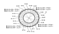
図2は、ヒータの各ヒータ要素であるハロゲンランプ16−01〜20の放射状の配置を示す平面図である。中央にリフレクター20a、20bが配置可能な円形の空間を設け、周囲に時計回りに20個のハロゲンランプが配置されている。その下側には、リフレクター18(上方の場合は18a、下方の場合は18b)が設けられる。図中ハロゲンランプ16−01、02、06、07、11、12、16、17からなる第1グループと、ハロゲンランプ16−03〜05、08〜10、13〜15、18〜20からなる第2グループとに分かれており、それぞれのグループに対応した傾斜部を備える2種類のリフレクターを準備した。第1のリフレクターは、第1グループに傾斜部を備えるものであり、第2のリフレクターは、第2グループに傾斜部を備えるものである。そのため、第1のリフレクターでは、傾斜部が2:3の割合で設けられ、第2のリフレクターでは、傾斜部が3:2の割合で設けられることになる。それぞれの傾斜部は、図1のシリコンウェーハ12の中心部に向かってより多くの熱線を反射するように所定の角度(例えば、7度)で傾斜している。
FIG. 2 is a plan view showing a radial arrangement of halogen lamps 16-01 to 20 which are heater elements of the heater. A circular space in which the
図9に、この傾斜角を図解する。リフレクター18a、18bから(特にリフレクターの半径方向中央16a−c、16b−cから)シリコンウェーハ12迄の鉛直方向の距離をHa、Hbとし、リフレクター18a、18bの置かれる平面内で、シリコンウェーハ12の中心に相当する中心までの距離をLa、Lbとすれば、Δa=tan−1(Ha/La)であり、Δb=tan−1(Hb/Lb)である。ここで、所定の角度αa、αbは、0<αa<π/2−Δaであり、0<αb<π/2−Δbである。ここで、高さが相対的に大きい場合、Δa、Δbは大きくなるので、傾斜角はそれほど大きくする必要もないと考えられ、αa、αbは小さくなる傾向がある。一方、高さが相対的に小さい場合、Δa、Δbは小さくなるので、傾斜角はそれほど小さくする必要もないと考えられ、αa、αbは大きくなる傾向がある。通常のHa/La、Hb/Lbにおいては、この傾斜角αa、αbは、それぞれ2度以上が好ましく、4度以上がより好ましく、5度以上が更に好ましい。また、この傾斜角αa、αbは、それぞれ12度以下が好ましく、10度以下がより好ましく、8度以下が更に好ましい。概ね7度が好ましいと考えられる。尚、傾斜角αa、αbは同じである必要はない。装置の各機器の配置に応じて適宜選択できる。ここで、La、Lbはハロゲンランプの半径方向で中央の位置から中心までの距離を意味してよい。また、これらの数値が同一でない場合は、算術平均して求めることができる。加熱されるシリコンウェーハ12及びサセプタ14は、同一中心軸の回りに回転するため、このように回転対象に備えられたヒータにより、均一に加熱される。
FIG. 9 illustrates this inclination angle. The vertical distances from the
図3は、図1の装置により、第1のリフレクターを上下に備えることにより、エピタキシャルウェーハを製造したときの、シリコンウェーハの温度及び各ヒータ(ヒータ要素)の出力の経時変化を示す。まず、任意単位の時間2までは、上下のハロゲンランプによりシリコンウェーハ(シリコン単結晶基板)を加熱し、熱処理を行った。到達最高温度は、任意単位の温度5であった。即ち、平均昇温速度は、約5/2=約2.5であった。次に、ヒータの出力を弱め、冷却して、エピタキシャル成長工程に入った。ここでは、まずシリコンウェーハの温度を任意単位の温度4にして、次に所定の濃度の原料ガスを流し、回転させながらエピタキシャル成長を任意単位の時間2.5から4.5まで行った。その次に、ヒータの出力を最低にし、放冷した。
FIG. 3 shows temporal changes in the temperature of the silicon wafer and the output of each heater (heater element) when an epitaxial wafer is manufactured by providing the first reflectors at the top and bottom with the apparatus of FIG. First, up to an arbitrary unit of
このときのエピタキシャル成長条件を以下に記す。尚、この条件は、次に述べるエピタキシャル製造方法において同一であった。
キャリアガス 水素
原料ガス シランまたはトリクロロシランを5%
流量 混合ガスで、50リッター/分
The epitaxial growth conditions at this time are described below. This condition was the same in the epitaxial manufacturing method described below.
Carrier gas
図4は、図1の装置により、第2のリフレクターを上下に備えることにより、エピタキシャルウェーハを製造したときの、シリコンウェーハの温度及び各ヒータ(ヒータ要素)の出力の経時変化を示す。この図の任意単位の温度及び時間は、図3と同じであるので、両者をそのまま対比することができる。図3の場合に比べ、最高温度が温度5となるまでの時間が約1.4であり、平均昇温速度は、約5/1.4=約3.6とより高かった。このため、温度5での熱処理時間をより長期間維持することができた。
FIG. 4 shows changes over time in the temperature of the silicon wafer and the output of each heater (heater element) when an epitaxial wafer is manufactured by providing the second reflectors at the top and bottom with the apparatus of FIG. Since the temperature and time in arbitrary units in this figure are the same as those in FIG. 3, they can be directly compared. Compared to the case of FIG. 3, the time until the maximum temperature reached 5 was about 1.4, and the average rate of temperature increase was about 5 / 1.4 = about 3.6. For this reason, the heat treatment time at
表1及び2に、図3及び4の実験を含む、実験結果をまとめる。図3は、表1の50/50/50のものであり、転位フリー(転位が無い)ウェーハは、上面と下面の温度差が−25又は−30のときのみであった。ここで、50/50/50は、上下のヒータの出力割合が50%ずつであり(最初の50)、上方の傾斜部に対応する傾斜対応ヒータとそれ以外のヒータとの出力割合が50%ずつ(次の50)であり、下方の傾斜部に対応する傾斜対応ヒータとそれ以外のヒータとの出力割合が50%ずつ(最後の50)である。一方、図4は、表2の50/60/60のものであり、転位フリー(転位が無い)ウェーハは、上面と下面の温度差が−30のときのみであった。このように、ほぼ同じ転位フリーの状態が得られるにもかかわらず、熱処理の時間が多く取れ、処理時間が短くなる効果が、第2のリフレクターにより得ることができた。 Tables 1 and 2 summarize the experimental results, including the experiments of FIGS. FIG. 3 is the one of 50/50/50 in Table 1. The dislocation free (no dislocation) wafer was only when the temperature difference between the upper surface and the lower surface was −25 or −30. Here, 50/50/50 is that the output ratio of the upper and lower heaters is 50% each (first 50), and the output ratio of the heater corresponding to the inclination corresponding to the upper inclined portion and the other heaters is 50%. (The next 50), and the output ratio of the heater corresponding to the inclination corresponding to the lower inclined portion and the other heaters is 50% (the last 50). On the other hand, FIG. 4 is the one of 50/60/60 in Table 2, and the dislocation-free (no dislocation) wafer was only when the temperature difference between the upper surface and the lower surface was −30. Thus, despite the fact that almost the same dislocation-free state can be obtained, the second reflector can obtain the effect of taking a long heat treatment time and shortening the treatment time.
ここで、表1において、上面及び下面の温度差が大きいと、転位フリーに成り易いが、これは、昇温速度を遅くしたため、結果的に上面及び下面の温度差が大きくなったためである。即ち、表1において、温度差が大きくなると、昇温速度が低下する関係にある。また、第1のリフレクターでは、外周への熱の放射割合が高いため、内側の出力を大きくすると、全体では却って出力が低下し、昇温速度が低下する。そのため、転位フリーに成り易い領域が増加したのである。一方、表2では、同様に、上面及び下面の温度差が大きいと、転位フリーに成り易かった。これは、同様に昇温速度を遅くすることにより、結果的に上面及び下面の温度差が大きくなったためである。即ち、表2において、温度差が大きくなると、昇温速度が低下する関係にある。しかるに、第2のリフレクターでは、外周への熱の放射割合が低いため、内側の出力を大きくすると、全体も出力が増加し、昇温速度が高くなる。そのため、転位フリーに成り易い領域が減少したのである。 Here, in Table 1, when the temperature difference between the upper surface and the lower surface is large, dislocation is likely to occur, but this is because the temperature difference between the upper surface and the lower surface is increased because the rate of temperature increase is slowed. That is, in Table 1, as the temperature difference increases, the temperature rising rate decreases. Moreover, in the 1st reflector, since the radiation | emission ratio of the heat | fever to an outer periphery is high, if an inner side output is enlarged, an output will decline on the whole, and a temperature increase rate will fall. For this reason, the area that is likely to be dislocation free has increased. On the other hand, in Table 2, similarly, when the temperature difference between the upper surface and the lower surface is large, dislocation is likely to occur. This is because the temperature difference between the upper surface and the lower surface is increased as a result of similarly decreasing the temperature increase rate. That is, in Table 2, as the temperature difference increases, the temperature rising rate decreases. However, in the second reflector, since the radiation ratio of heat to the outer periphery is low , when the output on the inner side is increased, the output increases as a whole and the temperature raising rate is increased. As a result, the area that is likely to be dislocation free has decreased.

図5(a)〜(c)は、表1の50/40/40(a)、50/50/50(b)、50/60/60(c)のものをそれぞれプロットしたものである。傾斜対応ヒータ要素の出力割合が40%と低い場合(a)は、特に外周部での温度分布がばらついていることがわかる。また、中心部では温度差がほぼ0であるが、外周部では概ね10℃と面内においても差がみられた。傾斜対応ヒータ要素の出力割合が50%と中くらいの場合(b)でも、(a)に比べれば少ないものの、外周部での温度分布がばらついている。また、中心部では温度差がほぼ0であるが、外周部では概ね5℃と面内においても若干の差がみられた。傾斜対応ヒータ要素の出力割合が60%と高い場合(c)でも、(a)に比べればかなり少ないものの、外周部での温度分布がややばらついている。中心部では温度差がほぼ0であり、外周部でも数℃と面内の差も少なくなった。これらの結果、外周部での温度差が特に小さい場合は、昇温速度も低く、転位フリーの領域が大きくなったことがわかる。 5A to 5C are plots of 50/40/40 (a), 50/50/50 (b), and 50/60/60 (c) of Table 1, respectively. When the output ratio of the heater element corresponding to the inclination is as low as 40% (a), it can be seen that the temperature distribution varies particularly in the outer peripheral portion. Moreover, although the temperature difference was substantially zero in the central part, the difference was also observed in the plane at approximately 10 ° C. in the outer peripheral part. Even in the case where the output ratio of the heater element corresponding to the inclination is about 50% (b), the temperature distribution in the outer peripheral portion varies although it is smaller than that in (a). In addition, although the temperature difference is almost zero in the central portion, there is a slight difference even in the plane at about 5 ° C. in the outer peripheral portion. Even when the output ratio of the heater element corresponding to the inclination is as high as 60%, the temperature distribution in the outer peripheral portion is slightly varied, although it is considerably smaller than that in (a). The temperature difference was almost zero at the center, and the in-plane difference was reduced to several degrees C. at the outer periphery. As a result, it can be seen that when the temperature difference at the outer peripheral portion is particularly small, the rate of temperature increase is low and the dislocation-free region becomes large.
図6(a)〜(c)は、表2の50/40/40(a)、50/50/50(b)、50/60/60(c)のものをそれぞれプロットしたものである。これらの図から、傾斜対応ヒータ要素の出力割合が40%と低い場合(a)は、中間部での温度分布がばらついていることがわかる。また、中心部では温度差がほぼ0であるが、中間部で5℃くらい、外周部では2〜3℃くらいと面内の差は図5の場合に比べ少なかった。しかし、図6の中では、一番面内の温度差が大きい。傾斜対応ヒータ要素の出力割合が50%と中くらいの場合(b)でも、(a)に比べれば少ないものの、中間部で2〜3℃くらいを中心にばらついているが、外周部では温度差もばらつきも殆どなかった。従って、面内の温度差分布のばらつきはあまり大きくなかった。傾斜対応ヒータ要素の出力割合が60%と高い場合(c)では、(a)及び(b)に比べればかなり少ないものの、中間部での温度分布がややばらついている。中心部では温度差がほぼ0であるが、外周部では、マイナス数℃外周部での温度差の逆転が生じていた。このように何れの外周部においても、温度差や温度差のばらつきは小さく、昇温速度が低くなる(a)の場合の方が、転位フリーの領域が大きくなったことがわかる。 6A to 6C are plots of 50/40/40 (a), 50/50/50 (b), and 50/60/60 (c) of Table 2, respectively. From these figures, it can be seen that when the output ratio of the inclination corresponding heater element is as low as 40% (a), the temperature distribution in the intermediate portion varies. Further, although the temperature difference is almost 0 in the central portion, the difference in the plane is about 5 ° C. in the middle portion and about 2-3 ° C. in the outer peripheral portion, which is smaller than that in the case of FIG. However, the in-plane temperature difference is the largest in FIG. Even if the output ratio of the heater element corresponding to the inclination is about 50% (b), although it is less than (a), it is scattered around 2 to 3 ° C in the middle part, but the temperature difference in the outer part There was almost no variation. Therefore, the variation in the in-plane temperature difference distribution was not so large. When the output ratio of the heater element corresponding to the inclination is as high as 60%, the temperature distribution in the middle part is slightly different in (c) although it is considerably smaller than (a) and (b). Although the temperature difference is substantially zero at the center, the temperature difference is reversed at the outer periphery at a minus several degrees Celsius. Thus, it can be seen that in any of the outer peripheral portions, the temperature difference and the variation in the temperature difference are small, and the dislocation-free region is larger in the case of (a) where the rate of temperature increase is low.
図7は、エピタキシャルウェーハ製造装置210における、シリコンウェーハ12及びサセプタ14を加熱する上部ヒータ16a、16a及び下部ヒータ16b、16b、並びに、背面にあるそれぞれのリフレクター18a、18b、並びに、円筒形の中央のリフレクター20a、20bを模式的に示し、熱線200a、200bにより、熱の移動を説明する図である。上部及び下部ヒータ16a、16a、16b、16bからは、各発光点より半球面に広がるように熱線が放射される。この熱線は、それぞれにほぼ同じ熱量を表わすので、当たる熱線の数が多い方が、熱が多く移動することになる。上部及び下部ヒータ16a、16a、16b、16bのシリコンウェーハ12及びサセプタ14に面する面よりは、熱線200a、200bが放射し、シリコンウェーハ12の表面、サセプタ14の上面及び底面に当たり熱を伝達する。また、リフレクター20a、20bの筒状部21a、21b及びコーン部22a、22bに当たった熱線は、反射角の法則に従い反射し、殆どそのままの熱量を反射熱線が運び、反射熱線が当たる部位に熱を伝える。従って、シリコンウェーハ12は、その主表面に当たる熱線の数で流入熱量が殆ど決定され、サセプタ14は、その上面の外縁(シリコンウェーハ12の外側)において、及び、底面全体において当たる熱線の数で流入熱量が殆ど決定される。
FIG. 7 shows the
図8は、上部及び下部ヒータ16a、16a、16b、16bの背面側より放射される熱線がリフレクター18においてどのように反射されるかを模式的に示す図である。図8(a)は、通常の水平に配置されたリフレクター18における反射の様子を、図8(b)は、所定の割合で設けられた傾斜部19における反射の様子を模式的に示すものである。上述するように、ヒータ16のシリコンウェーハ12側面の各輝点161から、半球状に発光熱線が放射され、シリコンウェーハ12側から見て背面側の面の各輝点162、163において同様に発光熱線が放射される。それぞれの熱線は、通常のリフレクター18の表面164において反射され、ほぼ均等に広がることがわかる。一方、傾斜部19の表面165においては、傾斜角βだけ、傾斜して反射されるため、シリコンウェーハ12の中心部(図中右側)に向かってより多くの熱線が反射されることがわかる。従って、シリコンウェーハ12側から見て背面側の面の各輝点162、163において、その面に対し角度θで放射された熱線は、その面に対しπ−θ+2×βの角度で反射されることになる。これらの関係を数式で示す。
反射角(通常)=π−θ (式1)
反射角(傾斜角β)=π−θ+2×β (式2)
FIG. 8 is a diagram schematically showing how the heat rays radiated from the back side of the upper and
Reflection angle (normal) = π−θ (Formula 1)
Reflection angle (tilt angle β) = π−θ + 2 × β (Formula 2)
100、210 エピタキシャルウェーハ製造装置
12 シリコンウェーハ
14 サセプタ
16、16a、16b ハロゲンランプ
18、18a、18b リフレクター
19 傾斜部
20a、20b 円筒状のリフレクター
32、34 放射熱温度計
100, 210 Epitaxial
Claims (2)
少なくとも前記シリコン単結晶基板の上及び/又は下に平面視で前記シリコン単結晶基板の中心部から放射状に配されるヒータと、
前記シリコン単結晶基板から見て前記ヒータの背後に前記シリコン単結晶基板の中心に垂直に立つ中心軸に対して回転対称に配置されるリフレクターと、
前記シリコン単結晶基板の温度を計測するウェーハ温度計と、
前記サセプタの温度を計測するサセプタ温度計と、
前記ヒータの出力を制御可能な制御装置と、を備え、
前記リフレクターは、前記ヒータから後ろ向きに放射される熱線を受けて前記シリコン単結晶基板の中心部に向かって、前記シリコン単結晶基板の外周部より、多くの割合で熱を反射するように傾斜した傾斜部を60%以上の割合で備え、
前記ヒータは、前記傾斜部に対応する傾斜部対応ヒータ要素を備え、
前記制御装置は、前記傾斜部対応ヒータ要素の出力の出力割合を60%以下として、必要に応じて全体の出力を増減させることにより、計測した前記シリコン単結晶基板の温度と前記サセプタの温度との差が、10℃以下となるように前記傾斜部対応ヒータ要素の出力を制御することを特徴とするエピタキシャルウェーハの製造装置。 An epitaxial wafer manufacturing apparatus for growing an epitaxial layer on a main surface of a silicon single crystal substrate disposed substantially horizontally on a susceptor,
A heater arranged radially from the center of the silicon single crystal substrate in a plan view above and / or below the silicon single crystal substrate;
A reflector disposed rotationally symmetrically with respect to a central axis standing perpendicular to the center of the silicon single crystal substrate behind the heater as viewed from the silicon single crystal substrate;
A wafer thermometer for measuring the temperature of the silicon single crystal substrate;
A susceptor thermometer for measuring the temperature of the susceptor;
A control device capable of controlling the output of the heater,
The reflector is inclined so as to reflect heat at a higher rate than the outer peripheral portion of the silicon single crystal substrate toward the central portion of the silicon single crystal substrate in response to heat rays emitted backward from the heater. Provide the sloped part at a rate of 60% or more ,
The heater includes an inclined portion corresponding heater element corresponding to the inclined portion,
The control device sets the output ratio of the heater element corresponding to the inclined portion to 60% or less, and increases or decreases the total output as necessary, thereby measuring the temperature of the silicon single crystal substrate and the temperature of the susceptor. The epitaxial wafer manufacturing apparatus is characterized in that the output of the heater element corresponding to the inclined portion is controlled such that the difference between them is 10 ° C. or less .
前記シリコン単結晶基板の上及び/又は下に配されるヒータにより非酸化性雰囲気で所定の温度に前記シリコン単結晶基板を加熱する工程と、
加熱された前記シリコン単結晶基板を所定のエピタキシャル成長温度まで冷却する工程と、
前記シリコン単結晶基板の主表面にエピタキシャル層を所定の温度で成長させる工程と、
前記シリコン単結晶基板の主表面にエピタキシャル層を成長させたエピタキシャルウェーハを冷却する工程と、を含み、
上記何れの工程においても、前記シリコン単結晶基板の温度と前記サセプタの温度との差を10℃以下にするように、前記ヒータにより制御し、
前記シリコン単結晶基板から見て平面視で前記シリコン単結晶基板の中心部から放射状に前記ヒータの背後に、各々前記シリコン単結晶基板の中心に垂直に立つ中心軸に対して回転対称に配置されるリフレクターが、前記ヒータから後ろ向きに放射される熱線を前記シリコン単結晶基板の中心部に向かって、前記シリコン単結晶基板の外周部より、多くの割合で熱を反射するように傾斜した傾斜部を60%以上の割合で備え、前記ヒータは、前記傾斜部に対応する傾斜部対応ヒータ要素を備え、前記傾斜部対応ヒータ要素の出力の出力割合を60%以下として、必要に応じて全体の出力を増減させることにより、前記傾斜部対応ヒータ要素の出力を制御することを特徴とするエピタキシャルウェーハの製造方法。
An epitaxial wafer manufacturing method for growing an epitaxial layer on a main surface of a silicon single crystal substrate disposed substantially horizontally on a susceptor,
Heating the silicon single crystal substrate to a predetermined temperature in a non-oxidizing atmosphere by a heater disposed on and / or below the silicon single crystal substrate;
Cooling the heated silicon single crystal substrate to a predetermined epitaxial growth temperature;
Growing an epitaxial layer on the main surface of the silicon single crystal substrate at a predetermined temperature;
Cooling an epitaxial wafer having an epitaxial layer grown on the main surface of the silicon single crystal substrate,
In any of the above steps, the heater is controlled so that the difference between the temperature of the silicon single crystal substrate and the temperature of the susceptor is 10 ° C. or less.
In a plan view when viewed from the silicon single crystal substrate, they are arranged behind the heater radially from the center of the silicon single crystal substrate and rotationally symmetrical with respect to a central axis that stands perpendicular to the center of the silicon single crystal substrate. The reflector is inclined such that heat rays emitted backward from the heater are reflected toward the center of the silicon single crystal substrate at a higher rate than the outer periphery of the silicon single crystal substrate. 60% or more, and the heater includes an inclined portion corresponding heater element corresponding to the inclined portion, and the output ratio of the output of the inclined portion corresponding heater element is set to 60% or less. A method of manufacturing an epitaxial wafer , wherein the output of the heater element corresponding to the inclined portion is controlled by increasing or decreasing the output.
Priority Applications (1)
| Application Number | Priority Date | Filing Date | Title |
|---|---|---|---|
| JP2008324795A JP5191373B2 (en) | 2008-12-19 | 2008-12-19 | Epitaxial wafer manufacturing method and manufacturing apparatus |
Applications Claiming Priority (1)
| Application Number | Priority Date | Filing Date | Title |
|---|---|---|---|
| JP2008324795A JP5191373B2 (en) | 2008-12-19 | 2008-12-19 | Epitaxial wafer manufacturing method and manufacturing apparatus |
Publications (3)
| Publication Number | Publication Date |
|---|---|
| JP2010147350A JP2010147350A (en) | 2010-07-01 |
| JP2010147350A5 JP2010147350A5 (en) | 2012-08-30 |
| JP5191373B2 true JP5191373B2 (en) | 2013-05-08 |
Family
ID=42567436
Family Applications (1)
| Application Number | Title | Priority Date | Filing Date |
|---|---|---|---|
| JP2008324795A Active JP5191373B2 (en) | 2008-12-19 | 2008-12-19 | Epitaxial wafer manufacturing method and manufacturing apparatus |
Country Status (1)
| Country | Link |
|---|---|
| JP (1) | JP5191373B2 (en) |
Cited By (1)
| Publication number | Priority date | Publication date | Assignee | Title |
|---|---|---|---|---|
| JP7004888B2 (en) | 2016-04-15 | 2022-01-21 | 日本ソリッド株式会社 | Oil collecting weir with diffusion prevention function |
Families Citing this family (12)
| Publication number | Priority date | Publication date | Assignee | Title |
|---|---|---|---|---|
| JP5807522B2 (en) * | 2011-11-17 | 2015-11-10 | 信越半導体株式会社 | Epitaxial growth equipment |
| US9200965B2 (en) * | 2012-06-26 | 2015-12-01 | Veeco Instruments Inc. | Temperature control for GaN based materials |
| JP2014060219A (en) * | 2012-09-14 | 2014-04-03 | Shin Etsu Handotai Co Ltd | Epitaxial growth apparatus |
| JP5920188B2 (en) * | 2012-11-26 | 2016-05-18 | 信越半導体株式会社 | Heating device |
| JP5602903B2 (en) | 2013-03-14 | 2014-10-08 | アプライド マテリアルズ インコーポレイテッド | Epitaxial film formation method and epitaxial growth apparatus |
| KR102116508B1 (en) * | 2013-08-29 | 2020-05-28 | 에스케이실트론 주식회사 | Apparatus for manufacturing epitaxial wafer |
| JP6198584B2 (en) * | 2013-11-21 | 2017-09-20 | アプライド マテリアルズ インコーポレイテッドApplied Materials,Incorporated | Epitaxial film formation method and epitaxial growth apparatus |
| JP6309252B2 (en) * | 2013-11-21 | 2018-04-11 | アプライド マテリアルズ インコーポレイテッドApplied Materials,Incorporated | Epitaxial film formation method and epitaxial growth apparatus |
| JP6241277B2 (en) * | 2013-12-27 | 2017-12-06 | 株式会社Sumco | Epitaxial growth equipment |
| EP3488464B1 (en) * | 2016-07-22 | 2021-09-08 | Applied Materials, Inc. | Heating modulators to improve epi uniformity tuning |
| US10446420B2 (en) | 2016-08-19 | 2019-10-15 | Applied Materials, Inc. | Upper cone for epitaxy chamber |
| CN111599722B (en) * | 2020-05-25 | 2023-04-14 | 北京北方华创微电子装备有限公司 | Semiconductor process equipment |
Family Cites Families (5)
| Publication number | Priority date | Publication date | Assignee | Title |
|---|---|---|---|---|
| JPH03150365A (en) * | 1989-07-26 | 1991-06-26 | Tokyo Electron Ltd | Heat treating device |
| US6064799A (en) * | 1998-04-30 | 2000-05-16 | Applied Materials, Inc. | Method and apparatus for controlling the radial temperature gradient of a wafer while ramping the wafer temperature |
| JP2000138170A (en) * | 1998-10-30 | 2000-05-16 | Applied Materials Inc | Semiconductor equipment |
| JP2002217110A (en) * | 2000-12-27 | 2002-08-02 | Applied Materials Inc | Heating apparatus and semiconductor manufacturing apparatus using the same |
| JP2004533118A (en) * | 2001-05-30 | 2004-10-28 | エーエスエム アメリカ インコーポレイテッド | Low temperature loading and unloading and baking |
-
2008
- 2008-12-19 JP JP2008324795A patent/JP5191373B2/en active Active
Cited By (1)
| Publication number | Priority date | Publication date | Assignee | Title |
|---|---|---|---|---|
| JP7004888B2 (en) | 2016-04-15 | 2022-01-21 | 日本ソリッド株式会社 | Oil collecting weir with diffusion prevention function |
Also Published As
| Publication number | Publication date |
|---|---|
| JP2010147350A (en) | 2010-07-01 |
Similar Documents
| Publication | Publication Date | Title |
|---|---|---|
| JP5191373B2 (en) | Epitaxial wafer manufacturing method and manufacturing apparatus | |
| TWI512884B (en) | Improved edge ring lip | |
| KR102226246B1 (en) | Multizone control of lamps in a conical lamphead using pyrometers | |
| US9558982B2 (en) | Minimal contact edge ring for rapid thermal processing | |
| JP3296300B2 (en) | Light irradiation type heating device | |
| CN107731718B (en) | Support cylinder for thermal processing chamber | |
| TWI625821B (en) | Substrate support ring for more uniform layer thickness | |
| JP6424726B2 (en) | Susceptor and epitaxial growth apparatus | |
| JP2010147350A5 (en) | ||
| US20200045776A1 (en) | Multizone lamp control and individual lamp control in a lamphead | |
| JP7107949B2 (en) | carrier ring | |
| JP5098873B2 (en) | Susceptor and vapor phase growth apparatus for vapor phase growth apparatus | |
| JP2002151412A (en) | Semiconductor manufacturing apparatus | |
| JP2007273623A (en) | Method and device for manufacturing epitaxial wafer | |
| KR102177620B1 (en) | Reflective liners | |
| JP6844529B2 (en) | Epitaxial wafer manufacturing method and epitaxial wafer | |
| JP2010141060A (en) | Method of manufacturing epitaxial silicon wafer | |
| JPWO2003003432A1 (en) | Vapor phase growth method and vapor phase growth apparatus | |
| KR20160024165A (en) | Apparatus for Manufacturing Wafer | |
| JPH0620950A (en) | Heater for substrate and using method of the heater | |
| JPS6358925A (en) | Vapor phase surface-treating reactor |
Legal Events
| Date | Code | Title | Description |
|---|---|---|---|
| A521 | Request for written amendment filed |
Free format text: JAPANESE INTERMEDIATE CODE: A523 Effective date: 20111214 |
|
| A621 | Written request for application examination |
Free format text: JAPANESE INTERMEDIATE CODE: A621 Effective date: 20111214 |
|
| A521 | Request for written amendment filed |
Free format text: JAPANESE INTERMEDIATE CODE: A523 Effective date: 20120711 |
|
| A977 | Report on retrieval |
Free format text: JAPANESE INTERMEDIATE CODE: A971007 Effective date: 20121024 |
|
| A131 | Notification of reasons for refusal |
Free format text: JAPANESE INTERMEDIATE CODE: A131 Effective date: 20121030 |
|
| A521 | Request for written amendment filed |
Free format text: JAPANESE INTERMEDIATE CODE: A523 Effective date: 20121226 |
|
| TRDD | Decision of grant or rejection written | ||
| A01 | Written decision to grant a patent or to grant a registration (utility model) |
Free format text: JAPANESE INTERMEDIATE CODE: A01 Effective date: 20130122 |
|
| A61 | First payment of annual fees (during grant procedure) |
Free format text: JAPANESE INTERMEDIATE CODE: A61 Effective date: 20130129 |
|
| R150 | Certificate of patent or registration of utility model |
Ref document number: 5191373 Country of ref document: JP Free format text: JAPANESE INTERMEDIATE CODE: R150 |
|
| FPAY | Renewal fee payment (event date is renewal date of database) |
Free format text: PAYMENT UNTIL: 20160208 Year of fee payment: 3 |
|
| R250 | Receipt of annual fees |
Free format text: JAPANESE INTERMEDIATE CODE: R250 |
|
| R250 | Receipt of annual fees |
Free format text: JAPANESE INTERMEDIATE CODE: R250 |
|
| R250 | Receipt of annual fees |
Free format text: JAPANESE INTERMEDIATE CODE: R250 |
|
| R250 | Receipt of annual fees |
Free format text: JAPANESE INTERMEDIATE CODE: R250 |
|
| R250 | Receipt of annual fees |
Free format text: JAPANESE INTERMEDIATE CODE: R250 |
|
| R250 | Receipt of annual fees |
Free format text: JAPANESE INTERMEDIATE CODE: R250 |
|
| R250 | Receipt of annual fees |
Free format text: JAPANESE INTERMEDIATE CODE: R250 |
|
| R250 | Receipt of annual fees |
Free format text: JAPANESE INTERMEDIATE CODE: R250 |
|
| R250 | Receipt of annual fees |
Free format text: JAPANESE INTERMEDIATE CODE: R250 |