JP5173496B2 - Imaging apparatus and imaging system - Google Patents
Imaging apparatus and imaging system Download PDFInfo
- Publication number
- JP5173496B2 JP5173496B2 JP2008056625A JP2008056625A JP5173496B2 JP 5173496 B2 JP5173496 B2 JP 5173496B2 JP 2008056625 A JP2008056625 A JP 2008056625A JP 2008056625 A JP2008056625 A JP 2008056625A JP 5173496 B2 JP5173496 B2 JP 5173496B2
- Authority
- JP
- Japan
- Prior art keywords
- imaging
- center
- pixel
- region
- photoelectric conversion
- Prior art date
- Legal status (The legal status is an assumption and is not a legal conclusion. Google has not performed a legal analysis and makes no representation as to the accuracy of the status listed.)
- Expired - Fee Related
Links
- 238000003384 imaging method Methods 0.000 title claims description 138
- 238000006243 chemical reaction Methods 0.000 claims description 77
- 239000004065 semiconductor Substances 0.000 claims description 48
- 238000012545 processing Methods 0.000 claims description 26
- 238000009792 diffusion process Methods 0.000 claims description 21
- 230000003287 optical effect Effects 0.000 claims description 19
- 230000002093 peripheral effect Effects 0.000 claims description 9
- 238000002955 isolation Methods 0.000 claims description 5
- 238000000034 method Methods 0.000 claims description 4
- 230000005484 gravity Effects 0.000 claims description 3
- 230000008569 process Effects 0.000 claims description 2
- 239000010410 layer Substances 0.000 description 33
- 238000010586 diagram Methods 0.000 description 16
- 238000012546 transfer Methods 0.000 description 16
- 239000000758 substrate Substances 0.000 description 12
- 239000012535 impurity Substances 0.000 description 10
- 238000005036 potential barrier Methods 0.000 description 9
- 238000009825 accumulation Methods 0.000 description 4
- 230000006870 function Effects 0.000 description 3
- 238000005468 ion implantation Methods 0.000 description 3
- 210000001747 pupil Anatomy 0.000 description 3
- 238000004364 calculation method Methods 0.000 description 2
- 239000011229 interlayer Substances 0.000 description 2
- 229910052581 Si3N4 Inorganic materials 0.000 description 1
- 230000003321 amplification Effects 0.000 description 1
- 230000004888 barrier function Effects 0.000 description 1
- 230000008859 change Effects 0.000 description 1
- 239000003086 colorant Substances 0.000 description 1
- 238000012937 correction Methods 0.000 description 1
- 238000013461 design Methods 0.000 description 1
- 239000002184 metal Substances 0.000 description 1
- 238000012986 modification Methods 0.000 description 1
- 230000004048 modification Effects 0.000 description 1
- 238000003199 nucleic acid amplification method Methods 0.000 description 1
- 229910021420 polycrystalline silicon Inorganic materials 0.000 description 1
- 229920005591 polysilicon Polymers 0.000 description 1
- 230000001681 protective effect Effects 0.000 description 1
- 230000035945 sensitivity Effects 0.000 description 1
- 238000000926 separation method Methods 0.000 description 1
- HQVNEWCFYHHQES-UHFFFAOYSA-N silicon nitride Chemical compound N12[Si]34N5[Si]62N3[Si]51N64 HQVNEWCFYHHQES-UHFFFAOYSA-N 0.000 description 1
Images


Classifications
-
- H—ELECTRICITY
- H01—ELECTRIC ELEMENTS
- H01L—SEMICONDUCTOR DEVICES NOT COVERED BY CLASS H10
- H01L27/00—Devices consisting of a plurality of semiconductor or other solid-state components formed in or on a common substrate
- H01L27/14—Devices consisting of a plurality of semiconductor or other solid-state components formed in or on a common substrate including semiconductor components sensitive to infrared radiation, light, electromagnetic radiation of shorter wavelength or corpuscular radiation and specially adapted either for the conversion of the energy of such radiation into electrical energy or for the control of electrical energy by such radiation
- H01L27/144—Devices controlled by radiation
- H01L27/146—Imager structures
- H01L27/14601—Structural or functional details thereof
- H01L27/14603—Special geometry or disposition of pixel-elements, address-lines or gate-electrodes
-
- H—ELECTRICITY
- H01—ELECTRIC ELEMENTS
- H01L—SEMICONDUCTOR DEVICES NOT COVERED BY CLASS H10
- H01L27/00—Devices consisting of a plurality of semiconductor or other solid-state components formed in or on a common substrate
- H01L27/14—Devices consisting of a plurality of semiconductor or other solid-state components formed in or on a common substrate including semiconductor components sensitive to infrared radiation, light, electromagnetic radiation of shorter wavelength or corpuscular radiation and specially adapted either for the conversion of the energy of such radiation into electrical energy or for the control of electrical energy by such radiation
- H01L27/144—Devices controlled by radiation
- H01L27/146—Imager structures
- H01L27/14601—Structural or functional details thereof
- H01L27/1463—Pixel isolation structures
-
- H—ELECTRICITY
- H01—ELECTRIC ELEMENTS
- H01L—SEMICONDUCTOR DEVICES NOT COVERED BY CLASS H10
- H01L27/00—Devices consisting of a plurality of semiconductor or other solid-state components formed in or on a common substrate
- H01L27/14—Devices consisting of a plurality of semiconductor or other solid-state components formed in or on a common substrate including semiconductor components sensitive to infrared radiation, light, electromagnetic radiation of shorter wavelength or corpuscular radiation and specially adapted either for the conversion of the energy of such radiation into electrical energy or for the control of electrical energy by such radiation
- H01L27/144—Devices controlled by radiation
- H01L27/146—Imager structures
- H01L27/14601—Structural or functional details thereof
- H01L27/14609—Pixel-elements with integrated switching, control, storage or amplification elements
-
- H—ELECTRICITY
- H01—ELECTRIC ELEMENTS
- H01L—SEMICONDUCTOR DEVICES NOT COVERED BY CLASS H10
- H01L27/00—Devices consisting of a plurality of semiconductor or other solid-state components formed in or on a common substrate
- H01L27/14—Devices consisting of a plurality of semiconductor or other solid-state components formed in or on a common substrate including semiconductor components sensitive to infrared radiation, light, electromagnetic radiation of shorter wavelength or corpuscular radiation and specially adapted either for the conversion of the energy of such radiation into electrical energy or for the control of electrical energy by such radiation
- H01L27/144—Devices controlled by radiation
- H01L27/146—Imager structures
- H01L27/14601—Structural or functional details thereof
- H01L27/14625—Optical elements or arrangements associated with the device
- H01L27/14627—Microlenses
-
- H—ELECTRICITY
- H01—ELECTRIC ELEMENTS
- H01L—SEMICONDUCTOR DEVICES NOT COVERED BY CLASS H10
- H01L27/00—Devices consisting of a plurality of semiconductor or other solid-state components formed in or on a common substrate
- H01L27/14—Devices consisting of a plurality of semiconductor or other solid-state components formed in or on a common substrate including semiconductor components sensitive to infrared radiation, light, electromagnetic radiation of shorter wavelength or corpuscular radiation and specially adapted either for the conversion of the energy of such radiation into electrical energy or for the control of electrical energy by such radiation
- H01L27/144—Devices controlled by radiation
- H01L27/146—Imager structures
- H01L27/14643—Photodiode arrays; MOS imagers
-
- H—ELECTRICITY
- H01—ELECTRIC ELEMENTS
- H01L—SEMICONDUCTOR DEVICES NOT COVERED BY CLASS H10
- H01L27/00—Devices consisting of a plurality of semiconductor or other solid-state components formed in or on a common substrate
- H01L27/14—Devices consisting of a plurality of semiconductor or other solid-state components formed in or on a common substrate including semiconductor components sensitive to infrared radiation, light, electromagnetic radiation of shorter wavelength or corpuscular radiation and specially adapted either for the conversion of the energy of such radiation into electrical energy or for the control of electrical energy by such radiation
- H01L27/144—Devices controlled by radiation
- H01L27/146—Imager structures
- H01L27/148—Charge coupled imagers
- H01L27/14831—Area CCD imagers
- H01L27/14843—Interline transfer
-
- H—ELECTRICITY
- H01—ELECTRIC ELEMENTS
- H01L—SEMICONDUCTOR DEVICES NOT COVERED BY CLASS H10
- H01L31/00—Semiconductor devices sensitive to infrared radiation, light, electromagnetic radiation of shorter wavelength or corpuscular radiation and specially adapted either for the conversion of the energy of such radiation into electrical energy or for the control of electrical energy by such radiation; Processes or apparatus specially adapted for the manufacture or treatment thereof or of parts thereof; Details thereof
- H01L31/0248—Semiconductor devices sensitive to infrared radiation, light, electromagnetic radiation of shorter wavelength or corpuscular radiation and specially adapted either for the conversion of the energy of such radiation into electrical energy or for the control of electrical energy by such radiation; Processes or apparatus specially adapted for the manufacture or treatment thereof or of parts thereof; Details thereof characterised by their semiconductor bodies
- H01L31/0352—Semiconductor devices sensitive to infrared radiation, light, electromagnetic radiation of shorter wavelength or corpuscular radiation and specially adapted either for the conversion of the energy of such radiation into electrical energy or for the control of electrical energy by such radiation; Processes or apparatus specially adapted for the manufacture or treatment thereof or of parts thereof; Details thereof characterised by their semiconductor bodies characterised by their shape or by the shapes, relative sizes or disposition of the semiconductor regions
- H01L31/035272—Semiconductor devices sensitive to infrared radiation, light, electromagnetic radiation of shorter wavelength or corpuscular radiation and specially adapted either for the conversion of the energy of such radiation into electrical energy or for the control of electrical energy by such radiation; Processes or apparatus specially adapted for the manufacture or treatment thereof or of parts thereof; Details thereof characterised by their semiconductor bodies characterised by their shape or by the shapes, relative sizes or disposition of the semiconductor regions characterised by at least one potential jump barrier or surface barrier
Description
本発明は、撮像装置及び撮像システムに関する。 The present invention relates to an imaging apparatus and an imaging system.
近年、ビデオカメラやディジタルスチルカメラ等において、CCD型イメージセンサやCMOS型イメージセンサ等の撮像装置が広く使用されている。撮像装置は、フォトダイオードを含む画素が2次元的に複数配列された撮像領域を有する。 In recent years, imaging devices such as CCD image sensors and CMOS image sensors are widely used in video cameras, digital still cameras, and the like. The imaging device has an imaging region in which a plurality of pixels including photodiodes are two-dimensionally arranged.
特許文献1に示された撮像装置では、図8に示すように、撮像領域の中心からの距離が遠くなるに従って、画素内におけるフォトダイオードPDへ入射する光の光軸PAc,PAb,PAaがその受光面の法線PLc,PLb,PLaに対して大きく傾く。この撮像装置では、フォトダイオードPDへ効率よく集光するために、フォトダイオードPDの上方にオンチップレンズ547が設けられている。そして、オンチップレンズ547とフォトダイオードPDとの間には、撮像領域の中心から画素までの距離(図8のc,b,aの順に距離が遠くなる)に応じて、光の光軸の傾きに沿うようにシフトされた信号線544,543,542が設けられている。これにより、特許文献1によれば、光軸が受光面の法線に対して大きく傾いても光を損失させずにフォトダイオードPDへ到達させるようにできるので、撮像領域の周辺部付近におけるフォトダイオードの受光感度を改善できるとされている。
In the imaging device disclosed in Patent Document 1, as shown in FIG. 8, as the distance from the center of the imaging region increases, the optical axes PAc, PAb, and PAa of light incident on the photodiode PD in the pixel are changed. It is greatly inclined with respect to the normal lines PLc, PLb and PLa of the light receiving surface. In this imaging device, an on-
特許文献2に示された撮像装置(CCD型イメージセンサ)では、撮像領域におけるその中心から所定の距離だけ離れた画素が、図9に示すような構成をしている。
In the imaging device (CCD type image sensor) disclosed in
特許文献2に示された技術では、撮像領域の中心から画素までの距離が遠くなるに従って、受光部(フォトダイオード)605へ入射する光の光軸PAがその受光面の法線PLに対して大きく傾く。この撮像装置では、受光部605へ効率よく集光するために、受光部605の上方であって光軸PAに沿った位置にオンチップレンズ650が設けられている。そして、受光部605内では、撮像領域の中心から画素までの距離に応じて、光の光軸PAの傾きに沿うようにシフトされた不純物領域605a〜605cが設けられている。これにより、特許文献2によれば、撮像領域の周辺部付近における斜め入射光によるスミアを抑制できるとされている。
特許文献1に示された撮像装置では、図8に示すように、フォトダイオードPDに入射した光が光電変換されて電荷が発生する領域CA1〜CA3が、撮像領域の中心から画素までの距離が遠くなるに従って、隣接する画素のフォトダイオードPDに近くなる。これにより、特定の画素のフォトダイオードPDで光電変換された電荷がその特定の画素に隣接する画素のフォトダイオードPDへ漏れ込む可能性がある。すなわち、斜め入射光により隣接する画素へ電荷が漏れこむ可能性がある。 In the imaging device disclosed in Patent Document 1, as shown in FIG. 8, the areas CA1 to CA3 where the light incident on the photodiode PD is photoelectrically converted to generate charges have a distance from the center of the imaging area to the pixel. As the distance increases, the pixel PD becomes closer to the photodiode PD of the adjacent pixel. As a result, the charge photoelectrically converted by the photodiode PD of the specific pixel may leak into the photodiode PD of the pixel adjacent to the specific pixel. That is, charges may leak into adjacent pixels due to oblique incident light.
特許文献2に記載された撮像装置では、受光部605とチャネルストッパ609との位置関係が撮像領域内の各画素の間で一様であると考えられる。この場合、受光部605に入射した光が光電変換されて電荷が発生する領域が、撮像領域の中心から画素までの距離が遠くなるに従って、チャネルストッパ609に近くなることがある。
In the imaging device described in
例えば、撮像領域内で図9に示す画素と撮像領域の中心に関して対称な画素では、受光部605の法線PLに対してチャネルストッパ609に近づく方向(図9の光軸PAと対称な方向)に光軸が傾いていると考えられる。この場合、受光部605におけるチャネルストッパ609に近い領域で斜め入射光が光電変換されるので、発生した電荷がチャネルストッパ609により形成されたポテンシャル障壁を越えて隣接する画素へ漏れこむ可能性がある。すなわち、斜め入射光により隣接する画素へ電荷が漏れこむ可能性がある。
For example, in a pixel symmetric with respect to the pixel shown in FIG. 9 and the center of the imaging region in the imaging region, a direction approaching the
本発明の目的は、斜め入射光による隣接する画素への電荷の漏れこみを抑制することにある。 An object of the present invention is to suppress charge leakage into adjacent pixels due to obliquely incident light.
本発明の第1側面に係る撮像装置は、光電変換部と、前記光電変換部を他の領域と分離するように素子分離領域の下に配置された半導体領域とを含む画素が2次元状に複数配列された撮像領域を有する撮像装置であって、前記画素内における前記光電変換部の受光面の中心を通る法線に対する前記半導体領域の少なくとも一部のオフセット量は、前記撮像領域の中心に配された画素に比べて前記撮像領域の周辺部に配された画素が大きいことを特徴とする。 In the imaging device according to the first aspect of the present invention, a pixel including a photoelectric conversion unit and a semiconductor region disposed under an element isolation region so as to separate the photoelectric conversion unit from other regions is two-dimensionally formed. An imaging apparatus having a plurality of imaging regions arranged, wherein an offset amount of at least a part of the semiconductor region with respect to a normal passing through a center of a light receiving surface of the photoelectric conversion unit in the pixel is at the center of the imaging region Compared with the arranged pixels, the pixels arranged in the peripheral part of the imaging region are larger.
本発明の第2側面に係る撮像システムは、上記の撮像装置と、前記撮像装置の撮像面へ像を形成する光学系と、前記撮像装置から出力された信号を処理して画像データを生成する信号処理部とを備えたことを特徴とする。 An imaging system according to a second aspect of the present invention generates image data by processing the imaging apparatus described above, an optical system that forms an image on an imaging surface of the imaging apparatus, and a signal output from the imaging apparatus. And a signal processing unit.
本発明によれば、斜め入射光による隣接する画素への電荷の漏れこみを抑制することができる。 According to the present invention, it is possible to suppress leakage of electric charges to adjacent pixels due to obliquely incident light.
本発明の第1実施形態に係る撮像装置100の概略構成について、図1を用いて説明する。図1は、第1実施形態に係る撮像装置100の概略構成を示す図である。
A schematic configuration of the
撮像装置100は、撮像領域IA、垂直走査回路79、列回路70、水平走査回路71、及び出力回路72を備える。
The
撮像領域IAでは、画素が2次元状に複数配列されている。図1には、撮像領域IAの中心RCに近い画素1c1,1c2と、その画素1c1,1c2より中心RCから遠い画素1b1,1b2と、画素1b1,1b2より中心RCから遠い画素1a1,1a2とが例示されている。画素1b1,1b2、1a1,1a2は画素1c1,1c2に比べて撮像領域の周辺部に配されているといえる。 In the imaging area IA, a plurality of pixels are arranged two-dimensionally. In FIG. 1, pixels 1c1 and 1c2 near the center RC of the imaging area IA, pixels 1b1 and 1b2 farther from the center RC than the pixels 1c1 and 1c2, and pixels 1a1 and 1a2 farther from the center RC than the pixels 1b1 and 1b2 are shown. Illustrated. It can be said that the pixels 1b1, 1b2, 1a1, and 1a2 are arranged in the periphery of the imaging region compared to the pixels 1c1 and 1c2.
垂直走査回路79は、撮像領域IAを垂直方向に走査することにより、撮像領域IAにおける各画素を駆動する。各画素は、駆動されることにより信号を出力する。
The
列回路70は、画素から出力された信号を受けて、所定期間だけその信号を保持する。
The
水平走査回路71は、列回路70を水平方向に走査することにより、列回路70により保持された信号を順次に出力回路72へ転送する。
The
出力回路72は、転送された信号を増幅して出力する。
The
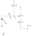
次に、各画素の構成を、図2を用いて説明する。図2は、各画素の回路構成を示す図である。図2には、画素1c2の回路構成が例示されているが、他の画素の回路構成も同様である。 Next, the configuration of each pixel will be described with reference to FIG. FIG. 2 is a diagram illustrating a circuit configuration of each pixel. FIG. 2 illustrates the circuit configuration of the pixel 1c2, but the circuit configurations of the other pixels are the same.
画素1c2は、光電変換部PD、転送部50、電荷電圧変換部7、出力部60、選択部30、及びリセット部40を含む。
The pixel 1c2 includes a photoelectric conversion unit PD, a
光電変換部PDは、受けた光を光電変換して電荷を発生させる。光電変換部PDは、例えば、フォトダイオードである。光電変換部PDは、電荷蓄積領域4を含む。
The photoelectric conversion unit PD generates charges by photoelectrically converting the received light. The photoelectric conversion unit PD is, for example, a photodiode. The photoelectric conversion unit PD includes a
転送部50は、光電変換部PDで発生した電荷を電荷電圧変換部7へ転送する。転送部50は、例えば、転送MOSトランジスタであり、そのゲート電極3に垂直走査回路79からアクティブな信号が供給された際に、オンして、光電変換部PDで発生した電荷を電荷電圧変換部7へ転送する。
The
電荷電圧変換部7は、電荷を電圧に変換する。電荷電圧変換部7は、光電変換部PDから転送された電荷を電圧に変換して、変換した電圧を出力部60へ入力する。電荷電圧変換部7は、例えば、フローティングディフュージョンである。
The charge-
出力部60は、電荷電圧変換部7から入力された電圧に応じた信号を選択部30経由で列信号線RLへ出力する。出力部60は、例えば、増幅MOSトランジスタであり、そのゲート電極に入力された電圧に応じた信号を増幅して、増幅した信号をソース経由で列信号線RLへ出力する。
The
選択部30は、画素が選択状態にされた際に、出力部60から出力された信号を列信号線RLへ転送する。選択部30は、例えば、選択MOSトランジスタであり、そのゲート電極に垂直走査回路79からアクティブな信号が供給された際に、オンして、出力部60から出力された信号を列信号線RLへ転送する。
The
リセット部40は、電荷電圧変換部7をリセットする。リセット部40は、例えば、リセットMOSトランジスタであり、そのゲート電極に垂直走査回路79からアクティブな信号が供給された際に、オンして、電荷電圧変換部7をリセットする。
The
次に、本発明の第1実施形態に係る撮像装置100における画素の断面構成について、図3を用いて説明する。図3のaは、図1におけるA−A’断面に対応する断面構成図である。図3のbは、図1におけるB−B’断面に対応する断面構成図である。図3のcは、図1におけるC−C’断面に対応する断面構成図である。
Next, a cross-sectional configuration of the pixel in the
19は、n型の不純物を含む半導体領域である。2は、n型の不純物を含む半導体領域であって、エピタキシャル成長により形成されたエピタキシャル層である。9は、p型の不純物を高濃度に含む半導体領域であって、電荷のオーバーフローバリアを形成する。
これらの領域は、例えば、次のように形成される。n型の不純物を含む下地基板を用意し、その下地基板の表面近傍にp型の不純物を注入することにより、下地基板内に半導体領域19及び半導体領域9を形成する。その後、下地基板の上にエピタキシャル層2をエピタキシャル成長させる。これにより、半導体基板SBが形成される。
These regions are formed as follows, for example. A base substrate containing an n-type impurity is prepared, and a p-type impurity is implanted near the surface of the base substrate, thereby forming a
なお、これらの領域は、他の方法で形成されても良い。例えば、半導体基板SBを準備して、その半導体基板SBに対してイオン注入を行うことにより半導体領域9やその上の半導体領域を形成しても良い。 Note that these regions may be formed by other methods. For example, the semiconductor region SB and the semiconductor region thereon may be formed by preparing the semiconductor substrate SB and performing ion implantation on the semiconductor substrate SB.
3は、ポリシリコンなどで形成された電極であって、転送部50(転送MOSトランジスタ)のゲート電極である。
4は、半導体基板SBの内部におけるn型の不純物を含む半導体領域であって、光電変換により発生した電荷を蓄積する電荷蓄積領域である。5は、半導体基板SBの表面におけるp型の不純物を含む半導体領域であって、電荷蓄積領域4を保護する保護領域である。エピタキシャル層2、電荷蓄積領域4、及び保護領域5は、光電変換部PD(埋め込み型のフォトダイオード)として機能するよう構成されている。光電変換部PDでは、エピタキシャル層2と電荷蓄積領域4との界面近傍で光電変換が行われ、発生した電荷が電荷蓄積領域4に蓄積される。このとき、保護領域5により暗電流が低減されている。また、電荷蓄積領域4は、転送部50(転送MOSトランジスタ)のソースとして機能する。
なお、光電変換部PDの構成は、埋め込み型以外の構成であってもよい。 The configuration of the photoelectric conversion unit PD may be a configuration other than the embedded type.
6は、絶縁膜(素子分離膜)を有しており、活性領域を他の活性領域と分離するための素子分離領域である。電荷電圧変換部7は、n型の不純物を高濃度に含む半導体領域であって、光電変換部PDにより転送された電荷を電圧に変換する領域(フローティングディフュージョン)である。電荷電圧変換部7は、転送部50(転送MOSトランジスタ)のドレインとして機能する。
13,14は、それぞれ、半導体基板SBの上方における所望の配線パターンを有するように形成された配線層である。配線層13,14は、例えば、金属で形成される。8,21,22は、それぞれ、ゲート電極3及び配線層13,14を互いに絶縁する層間絶縁膜である。15は、最上の層間絶縁膜22の上にプラズマシリコン窒化膜等で形成された層内レンズである。この層内レンズ15は、光電変換部PDの上方に配置されている。
23は、光電変換部PDの上方であって層内レンズ15の上に設けられた平坦化層である。16は、平坦化層23の上に設けられた層であり、複数の波長のいずれかの波長の光を選択的に透過するカラーフィルタを含むカラーフィルタ層である。カラーフィルタ層16に含まれるカラーフィルタは、例えば、RGBのいずれかの波長の光を選択的に透過する原色フィルターである。
17は、光電変換部PDの上方であってカラーフィルタ層16のカラーフィルタの上に設けられたマイクロレンズである。
10は、光電変換部PDを他の領域(他の画素の光電変換部PD)と分離するように素子分離領域6の下に配置された半導体領域である。半導体領域10は、複数の拡散層10a〜10dを含む。複数の拡散層10a〜10dは、それぞれ、p型の不純物を高濃度に含む層であり、電荷蓄積領域4に蓄積されるべき電荷に対するポテンシャル障壁を形成する。
ところで、撮像装置100に対して、用いられている撮影レンズ92の絞り93(図4参照)によって決定される射出瞳と呼ばれる擬似的な光源が存在する。レンズ焦点から射出瞳までの距離である射出瞳距離が有限であるために、撮像領域18の中心RCから周辺部へ行くに従って光電変換部PDに入射する光の光軸PAc〜PAaが法線PLc〜PLaに対して傾き、入射角度が大きくなる。
By the way, there exists a pseudo light source called an exit pupil determined by the diaphragm 93 (see FIG. 4) of the photographing
ここで、仮に、画素内における光電変換部を他の画素の光電変換部と分離するための半導体領域が、撮像領域の中心から画素までの距離に関わらず、光電変換部の受光面の中心を通る法線に対して一定のオフセット量を有している場合を考える。この場合、光電変換部PDにおけるその分離するための半導体領域に近い領域で斜め入射光が光電変換され得るので、発生した電荷がその半導体領域により形成されたポテンシャル障壁を越えて隣接する画素へ漏れこむ可能性がある。すなわち、斜め入射光により隣接する画素へ電荷が漏れこむ可能性がある。 Here, it is assumed that the semiconductor region for separating the photoelectric conversion unit in the pixel from the photoelectric conversion unit of another pixel is the center of the light receiving surface of the photoelectric conversion unit regardless of the distance from the center of the imaging region to the pixel. Consider a case in which there is a certain amount of offset with respect to the normal passing through. In this case, since obliquely incident light can be photoelectrically converted in a region near the semiconductor region for separation in the photoelectric conversion unit PD, the generated charge leaks to the adjacent pixel beyond the potential barrier formed by the semiconductor region. There is a possibility that That is, charges may leak into adjacent pixels due to oblique incident light.
それに対して、本実施形態の撮像装置100では、撮像領域18における各画素が次のような特徴を有する。すなわち、画素内における光電変換部PDの受光面の中心を通る法線PLc〜PLaに対する半導体領域10の少なくとも一部のオフセット量は、撮像領域18の中心に配された画素に比べて前記撮像領域の周辺部に配された画素が大きい。すなわち、画素内における光電変換部PDの受光面の中心を通る法線PLc〜PLaに対する半導体領域10の一部の拡散層10bのオフセット量OF1c〜OF1aは、撮像領域18の中心に配された画素に比べて前記撮像領域の周辺部に配された画素が大きい。
On the other hand, in the
例えば、撮像領域18の中心RC(図1参照)に近い画素1c2内では、法線PLcに対する拡散層10bのオフセット量がOF1cになる。中心RC(図1参照)から画素1c2より遠い画素1b2内では、法線PLbに対する拡散層10bのオフセット量がOF1b(>OF1c)になる。中心RC(図1参照)から画素1b2より遠い画素1a2内では、法線PLaに対する拡散層10bのオフセット量がOF1a(>OF1b)になる。すなわち、画素1c2,1b2,1a2内におけるオフセット量は、
OF1c<OF1b<OF1a・・・数式1の関係にある。ここで、異なるフォトマスクを用いて各拡散層10a〜10dごとにイオン注入を行うことにより、法線に対するオフセット量の互いに異なり得る複数の拡散層10a〜10dを得ることができる。
For example, in the pixel 1c2 close to the center RC (see FIG. 1) of the
OF1c <OF1b <OF1a (Equation 1). Here, by performing ion implantation for each of the diffusion layers 10a to 10d using different photomasks, it is possible to obtain a plurality of
このように、本実施形態によれば、画素内における光電変換部PDの光電変換が行われる領域とポテンシャル障壁を形成するための半導体領域との距離を、撮像領域18の各画素について均等にすることができる。このため、撮像領域の中心から画素までの距離が遠くなっても、光電変換により発生した電荷が半導体領域によるポテンシャル障壁を越えることを抑制できる。すなわち、斜め入射光による隣接する画素への電荷の漏れこみを抑制することができる。ここで光電変換部PDの光電変換が行われる領域とポテンシャル障壁を形成するための半導体領域との距離は全画素で全て等しくする必要はない。撮像領域の中心からの距離に応じて複数の領域に分け、領域ごとにオフセット量をかえることもできる。更にはセンサチップのサイズによっては中心に配された画素に比べてオフセット量を大きくする画素を撮像領域内の周辺部の最も外側に配される画素のみにしてもよい。
As described above, according to the present embodiment, the distance between the region where the photoelectric conversion of the photoelectric conversion unit PD is performed in the pixel and the semiconductor region for forming the potential barrier is equalized for each pixel in the
また、斜め入射光が光電変換の行われるべき領域を通過して隣接する画素の光電変換部へ到達することも抑制できる。 In addition, it is possible to prevent oblique incident light from passing through a region where photoelectric conversion is to be performed and reaching a photoelectric conversion unit of an adjacent pixel.
さらに、画素内におけるポテンシャル障壁を形成するための半導体領域以外の部分は、構造の変更がないので、撮像領域の各画素の間での特性ばらつきも抑制できる。これにより、例えば、転送トランジスタ(転送部)のチャネルやフォトダイオード(光電変換部)の空乏領域を考慮してフォトダイオード(光電変換部)を決定できるので、設計の自由度が高くなる。 Further, since the structure of the portion other than the semiconductor region for forming the potential barrier in the pixel is not changed, the characteristic variation among the pixels in the imaging region can be suppressed. Thereby, for example, the photodiode (photoelectric conversion unit) can be determined in consideration of the channel of the transfer transistor (transfer unit) and the depletion region of the photodiode (photoelectric conversion unit), so that the degree of freedom in design increases.
なお、撮像領域18の中心RCから距離に応じてオフセット量を変える半導体領域10内の拡散層は、拡散層10b以外の拡散層10a,10c,10dであっても良いし、拡散層10bと他の拡散層10a,10c,10dとの組み合わせでも良い。
Note that the diffusion layers in the
また、半導体領域10に含まれる拡散層の数は、図3に示される4つ以外であっても良い。
Further, the number of diffusion layers included in the
さらに、半導体領域10におけるオフセット量を変える部分及びそのオフセット量は、カラーフィルタにより透過される光の波長に応じて決定されていてもよい。
Furthermore, the portion of the
例えば、図5に示すように、撮像領域18の中心からの距離が画素1b2と同様だが、カラーフィルタにより透過される光の波長が互いに異なる画素1b21〜1b23を考える。画素1b21では、カラーフィルタ161により青色の波長の光が透過される。画素1b22では、カラーフィルタ162により緑色の波長の光が透過される。画素1b23では、カラーフィルタ163により赤色の波長の光が透過される。この場合、画素1b21内で光電変換が行われる領域は、半導体基板SBの表面に近く、画素1b23内で光電変換が行われる領域は、半導体基板SBの表面から深く、画素1b22内で光電変換が行われる領域は、両者の中間付近に位置している。この場合でも、半導体領域10における一部のオフセット量を、撮像領域18の中心RCから画素までの距離が遠くなるほど大きくなるように決定されている。半導体領域10におけるその一部は、カラーフィルタにより透過される光の波長が長いほど光電変換部PDの受光面から深く位置するように決定されている。そして、そのオフセット量OF1b1〜OF1b3は、撮像領域18の中心RCから画素までの距離が等しい場合、カラーフィルタ161〜163により透過される光の波長が長いほど大きくなるように決定されている。
For example, as illustrated in FIG. 5, consider pixels 1b21 to 1b23 that have the same distance from the center of the
これにより、画素内における光電変換部PDの光電変換が行われる領域とポテンシャル障壁を形成するための半導体領域との距離を、光電変換部PDへ入射する光の波長が画素の間で異なっても、撮像領域18の各画素について均等にすることができる。
Thereby, even if the wavelength of the light which injects into photoelectric conversion part PD differs between pixels, the distance of the area | region where photoelectric conversion of the photoelectric conversion part PD in a pixel is performed, and the semiconductor region for forming a potential barrier differs. The pixels in the
次に、本発明の撮像装置を適用した撮像システムの一例を図4に示す。 Next, an example of an imaging system to which the imaging apparatus of the present invention is applied is shown in FIG.
撮像システム90は、図4に示すように、主として、光学系、撮像装置100及び信号処理部を備える。光学系は、主として、シャッター91、撮影レンズ92及び絞り93を備える。信号処理部は、主として、撮像信号処理回路95、A/D変換器96、画像信号処理部97、メモリ部87、外部I/F部89、タイミング発生部98、全体制御・演算部99、記録媒体88及び記録媒体制御I/F部94を備える。なお、信号処理部は、記録媒体88を備えなくても良い。
As shown in FIG. 4, the
シャッター91は、光路上において撮影レンズ92の手前に設けられ、露出を制御する。
The
撮影レンズ92は、入射した光を屈折させて、撮像装置100の撮像領域18(撮像面)に被写体の像を形成する。
The
絞り93は、光路上において撮影レンズ92と撮像装置100との間に設けられ、撮影レンズ92を通過後に撮像装置100へ導かれる光の量を調節する。
The
撮像装置100は、撮像領域18に形成された被写体の像を画像信号に変換する。撮像装置100は、その画像信号を撮像領域18から読み出して出力する。
The
撮像信号処理回路95は、撮像装置100に接続されており、撮像装置100から出力された画像信号を処理する。
The imaging
A/D変換器96は、撮像信号処理回路95に接続されており、撮像信号処理回路95から出力された処理後の画像信号(アナログ信号)をデジタル信号へ変換する。
The A /
画像信号処理部97は、A/D変換器96に接続されており、A/D変換器96から出力された画像信号(デジタル信号)に各種の補正等の演算処理を行い、画像データを生成する。この画像データは、メモリ部87、外部I/F部89、全体制御・演算部99及び記録媒体制御I/F部94などへ供給される。
The image
メモリ部87は、画像信号処理部97に接続されており、画像信号処理部97から出力された画像データを記憶する。
The
外部I/F部89は、画像信号処理部97に接続されている。これにより、画像信号処理部97から出力された画像データを、外部I/F部89を介して外部の機器(パソコン等)へ転送する。
The external I /
タイミング発生部98は、撮像装置100、撮像信号処理回路95、A/D変換器96及び画像信号処理部97に接続されている。これにより、撮像装置*、撮像信号処理回路95、A/D変換器96及び画像信号処理部97へタイミング信号を供給する。そして、撮像装置100、撮像信号処理回路95、A/D変換器96及び画像信号処理部97がタイミング信号に同期して動作する。
The
全体制御・演算部99は、タイミング発生部98、画像信号処理部97及び記録媒体制御I/F部94に接続されており、タイミング発生部98、画像信号処理部97及び記録媒体制御I/F部94を全体的に制御する。
The overall control /
記録媒体88は、記録媒体制御I/F部94に取り外し可能に接続されている。これにより、画像信号処理部97から出力された画像データを、記録媒体制御I/F部94を介して記録媒体88へ記録する。
The recording medium 88 is detachably connected to the recording medium control I /
以上の構成により、撮像装置100において良好な画像信号が得られれば、良好な画像(画像データ)を得ることができる。
With the above configuration, if a good image signal is obtained in the
次に、本発明の第2実施形態に係る撮像装置について、図6を用いて説明する。図6は、本発明の第2実施形態に係る撮像装置における画素の断面構成を示す図である。図6のaは、図1におけるA−A’断面に対応する断面構成図である。図6のbは、図1におけるB−B’断面に対応する断面構成図である。図6のcは、図1におけるC−C’断面に対応する断面構成図である。以下では、第1実施形態と異なる部分を中心に説明し、同様の部分の説明を省略する。 Next, an imaging apparatus according to a second embodiment of the present invention will be described with reference to FIG. FIG. 6 is a diagram illustrating a cross-sectional configuration of a pixel in an imaging apparatus according to the second embodiment of the present invention. FIG. 6A is a cross-sectional configuration diagram corresponding to the A-A ′ cross section in FIG. 1. FIG. 6B is a cross-sectional configuration diagram corresponding to the B-B ′ cross section in FIG. 1. FIG. 6C is a cross-sectional configuration diagram corresponding to the C-C ′ cross section in FIG. 1. Below, it demonstrates centering on a different part from 1st Embodiment, and abbreviate | omits description of the same part.
本実施形態の撮像装置では、撮像領域18における各画素が次のような特徴を有する。すなわち、画素内における光電変換部PDの受光面の中心を通る法線PLc,PLb,PLaに対する半導体領域10の重心軸GAc,GAb,GAaの傾斜角は、撮像領域18の中心RCから画素までの距離が遠くなるほど大きくなるように決定されている。すなわち、画素内における半導体領域10の重心軸GAc,GAb,GAaは、光電変換部PDの受光面へ入射する光の光軸PAc,PAb,PAaに沿った方向に傾いている。
In the imaging apparatus of the present embodiment, each pixel in the
例えば、撮像領域18の中心RC(図1参照)に近い画素1c2内では、法線PLcに対する重心軸GAcの傾斜角がγ(≒0)になる。中心RC(図1参照)から画素1c2より遠い画素1b2内では、法線PLbに対する重心軸GAbの傾斜角がβ(>γ)になる。中心RC(図1参照)から画素1b2より遠い画素1a2内では、法線PLaに対する重心軸GAaの傾斜角がα(>β)になる。すなわち、画素1c2,1b2,1a2内における傾斜角は、
γ(≒0)<β<α・・・数式2
の関係にある。ここで、異なるフォトマスクを用いて各拡散層10a〜10dごとにイオン注入を行うことにより、法線に対するオフセット量の互いに異なる複数の拡散層10a〜10dを得ることができる。
For example, in the pixel 1c2 close to the center RC (see FIG. 1) of the
γ (≈0) <β <α (2)
Are in a relationship. Here, by performing ion implantation for each of the diffusion layers 10a to 10d using different photomasks, a plurality of
このように、本実施形態によれば、画素内における光電変換部PDの光電変換が行われる領域と半導体領域10との距離を、光電変換が行われる領域の深さが画素の間で異なっていても、撮像領域18の各画素について均等にすることができる。すなわち、画素内における光電変換部PDの光電変換が行われる領域と半導体領域10との距離を、光電変換部PDへ入射する光の波長が画素の間で異なっても、撮像領域18の各画素について均等にすることができる。ここで光電変換部PDの光電変換が行われる領域とポテンシャル障壁を形成するための半導体領域との距離は全画素で全て等しくする必要はない。撮像領域の中心からの距離に応じて複数の領域に分け、領域ごとにオフセット量をかえることもできる。更にはセンサチップのサイズによっては中心に配された画素に比べてオフセット量を大きくする画素を撮像領域内の周辺部の最も外側に配される画素のみにしてもよい。
As described above, according to the present embodiment, the distance between the region where the photoelectric conversion of the photoelectric conversion unit PD is performed in the pixel and the
また、全ての色に対応して、撮像領域18における隣接する画素の間で同様なシュリンク率でのレイアウトパターンを用いて各画素のパターンを形成することができる。
In addition, corresponding to all colors, a pattern of each pixel can be formed using a layout pattern with a similar shrink rate between adjacent pixels in the
次に、本発明の第3実施形態に係る撮像装置について、図7を用いて説明する。図7は、本発明の第3実施形態に係る撮像装置における画素の断面構成を示す図である。図7のaは、図1におけるA−A’断面に対応する断面構成図である。図7のbは、図1におけるB−B’断面に対応する断面構成図である。図7のcは、図1におけるC−C’断面に対応する断面構成図である。以下では、第1実施形態と異なる部分を中心に説明し、同様の部分の説明を省略する。 Next, an imaging device according to a third embodiment of the present invention will be described with reference to FIG. FIG. 7 is a diagram illustrating a cross-sectional configuration of a pixel in an imaging apparatus according to the third embodiment of the present invention. FIG. 7A is a cross-sectional configuration diagram corresponding to the A-A ′ cross section in FIG. 1. FIG. 7B is a cross-sectional configuration diagram corresponding to the B-B ′ cross section in FIG. 1. FIG. 7C is a cross-sectional configuration diagram corresponding to the C-C ′ cross section in FIG. 1. Below, it demonstrates centering on a different part from 1st Embodiment, and abbreviate | omits description of the same part.
本実施形態の撮像装置では、撮像領域18における各画素が次のような特徴を有する。すなわち、画素内における光電変換部PDの受光面の中心を通る法線PLc,PLb,PLaに対する要素の重心のオフセット量は、撮像領域18の中心RCから画素までの距離が遠くなるほど大きくなるように決定されている。ここで、要素は、マイクロレンズ17、カラーフィルタ16、層内レンズ15、及び配線層13,14の少なくとも1つを含む。
In the imaging apparatus of the present embodiment, each pixel in the
例えば、撮像領域18の中心RC(図1参照)に近い画素1c2内では、法線PLcに対するマイクロレンズ17のオフセット量がOF3c(≒0)になる。中心RC(図1参照)から画素1c2より遠い画素1b2内では、法線PLbに対するマイクロレンズ17のオフセット量がOF3b(>OF1c)になる。中心RC(図1参照)から画素1b2より遠い画素1a2内では、法線PLaに対するマイクロレンズ17のオフセット量がOF1a(>OF1b)になる。すなわち、画素1c2,1b2,1a2内におけるオフセット量は、
OF3c(≒0)<OF3b<OF3a・・・数式3
の関係にある。
For example, in the pixel 1c2 close to the center RC (see FIG. 1) of the
OF3c (≈0) <OF3b <OF3a (3)
Are in a relationship.
このように、本実施形態によれば、要素を光軸PAc〜PAaの傾きに沿うようにシフトさせるので、光軸PAc〜PAaが受光面の法線PLc〜PLaに対して大きく傾いても光を損失させずに光電変換部PDへ到達させるようにできる。 Thus, according to the present embodiment, the elements are shifted so as to follow the inclinations of the optical axes PAc to PAa. Therefore, even if the optical axes PAc to PAa are largely inclined with respect to the normal lines PLc to PLa of the light receiving surface, It can be made to reach the photoelectric conversion part PD without loss.
90 撮像システム
100 撮像装置
90
Claims (8)
前記画素内における前記光電変換部の受光面の中心を通る法線に対する前記半導体領域の少なくとも一部の、前記中心から遠ざかる方向へのオフセット量は、前記撮像領域の中心に配された画素に比べて前記撮像領域の周辺部に配された画素が大きい
ことを特徴とする撮像装置。 An imaging apparatus having an imaging region in which a plurality of pixels including a photoelectric conversion unit and a semiconductor region disposed under an element isolation region so as to separate the photoelectric conversion unit from other regions are arranged two-dimensionally. And
The offset amount in the direction away from the center of at least a part of the semiconductor region with respect to the normal passing through the center of the light receiving surface of the photoelectric conversion unit in the pixel is larger than that of the pixel arranged in the center of the imaging region An image pickup apparatus having a large number of pixels arranged in a peripheral portion of the image pickup area.
前記画素内における前記光電変換部の受光面の中心を通る法線に対する前記複数の拡散層の少なくとも1つの拡散層の、前記中心から遠ざかる方向へのオフセット量は、前記撮像領域の中心に配された画素に比べて前記撮像領域の周辺部に配された画素が大きい
ことを特徴とする請求項1に記載の撮像装置。 The semiconductor region includes a plurality of diffusion layers,
The offset amount in the direction away from the center of at least one diffusion layer of the plurality of diffusion layers with respect to the normal passing through the center of the light receiving surface of the photoelectric conversion unit in the pixel is arranged at the center of the imaging region. The imaging device according to claim 1, wherein pixels arranged in a peripheral portion of the imaging region are larger than the arranged pixels.
前記画素内における前記光電変換部の受光面の中心を通る法線に対する前記重心軸の傾斜角は、前記撮像領域の中心に配された画素に比べて前記撮像領域の周辺部に配された画素が大きい
ことを特徴とする請求項1又は2に記載の撮像装置。 The center of gravity axis of the semiconductor region in the pixel is inclined in a direction along the optical axis of the light incident on the light receiving surface of the photoelectric conversion unit,
Pixel inclination angle of the central axis with respect to the normal line, arranged on the periphery of the imaging area than the pixels arranged in the center of the imaging area through the center of the light receiving surface of the photoelectric conversion portion in said pixel The imaging device according to claim 1, wherein the imaging device is large.
前記半導体領域の一部の、前記中心から遠ざかる方向へのオフセット量は、前記撮像領域の中心に配された画素に比べて前記撮像領域の周辺部に配された画素が大きく、
前記半導体領域における前記一部は、前記カラーフィルタにより透過される光の波長が長いほど前記光電変換部の受光面から深く位置するように決定されている
ことを特徴とする請求項1から3のいずれか1項に記載の撮像装置。 The pixel further includes a color filter that selectively transmits light of any one of the wavelengths such that light of any of the plurality of wavelengths enters the photoelectric conversion unit,
The offset amount in the direction away from the center of a part of the semiconductor region is larger in the pixels arranged in the peripheral part of the imaging region than the pixels arranged in the center of the imaging region,
Said portion of said semiconductor region, of claims 1 to 3, characterized in that the wavelength of the light transmitted is determined to be located deeper from longer receiving surface of the photoelectric conversion unit by the color filter The imaging device according to any one of the above.
ことを特徴とする請求項4に記載の撮像装置。 The offset amount, a plurality of pixels equal distance from the center of the imaging area, in claim 4, wherein the wavelength of the light transmitted by the color filter is determined to be larger the longer The imaging device described.
前記画素内における前記光電変換部の受光面の中心を通る法線に対する前記要素の重心の、前記中心から遠ざかる方向へのオフセット量は、前記撮像領域の中心に配された画素に比べて前記撮像領域の周辺部に配された画素が大きい
ことを特徴とする請求項1から3のいずれか1項に記載の撮像装置。 The pixel further includes an element disposed above the photoelectric conversion unit,
The amount of offset of the center of gravity of the element in the direction away from the center with respect to the normal passing through the center of the light receiving surface of the photoelectric conversion unit in the pixel is larger than that of the pixel arranged at the center of the imaging region. The imaging device according to any one of claims 1 to 3 , wherein pixels arranged in a peripheral portion of the region are large.
ことを特徴とする請求項6に記載の撮像装置。 The imaging device according to claim 6 , wherein the element includes at least one of a microlens, a color filter, an in-layer lens, and a wiring layer.
前記撮像装置の撮像面へ像を形成する光学系と、
前記撮像装置から出力された信号を処理して画像データを生成する信号処理部と、
を備えたことを特徴とする撮像システム。 The imaging device according to any one of claims 1 to 7,
An optical system for forming an image on the imaging surface of the imaging device;
A signal processing unit that processes the signal output from the imaging device to generate image data;
An imaging system comprising:
Priority Applications (3)
| Application Number | Priority Date | Filing Date | Title |
|---|---|---|---|
| JP2008056625A JP5173496B2 (en) | 2008-03-06 | 2008-03-06 | Imaging apparatus and imaging system |
| US12/370,928 US7812382B2 (en) | 2008-03-06 | 2009-02-13 | Image sensing apparatus and imaging system |
| CN2009100079722A CN101527311B (en) | 2008-03-06 | 2009-03-06 | Image sensing apparatus and imaging system |
Applications Claiming Priority (1)
| Application Number | Priority Date | Filing Date | Title |
|---|---|---|---|
| JP2008056625A JP5173496B2 (en) | 2008-03-06 | 2008-03-06 | Imaging apparatus and imaging system |
Publications (3)
| Publication Number | Publication Date |
|---|---|
| JP2009212465A JP2009212465A (en) | 2009-09-17 |
| JP2009212465A5 JP2009212465A5 (en) | 2011-03-17 |
| JP5173496B2 true JP5173496B2 (en) | 2013-04-03 |
Family
ID=41052729
Family Applications (1)
| Application Number | Title | Priority Date | Filing Date |
|---|---|---|---|
| JP2008056625A Expired - Fee Related JP5173496B2 (en) | 2008-03-06 | 2008-03-06 | Imaging apparatus and imaging system |
Country Status (3)
| Country | Link |
|---|---|
| US (1) | US7812382B2 (en) |
| JP (1) | JP5173496B2 (en) |
| CN (1) | CN101527311B (en) |
Families Citing this family (12)
| Publication number | Priority date | Publication date | Assignee | Title |
|---|---|---|---|---|
| JP2010239001A (en) * | 2009-03-31 | 2010-10-21 | Sony Corp | Capacitive element, method of manufacturing the same, solid-state image pickup device, and imaging device |
| JP5585232B2 (en) | 2010-06-18 | 2014-09-10 | ソニー株式会社 | Solid-state imaging device, electronic equipment |
| JP2013004635A (en) * | 2011-06-14 | 2013-01-07 | Canon Inc | Image sensor, imaging device, and formation method |
| JP6141024B2 (en) | 2012-02-10 | 2017-06-07 | キヤノン株式会社 | Imaging apparatus and imaging system |
| JP5956840B2 (en) | 2012-06-20 | 2016-07-27 | キヤノン株式会社 | Solid-state imaging device and camera |
| CN104904197B (en) * | 2012-12-05 | 2016-12-28 | 富士胶片株式会社 | Camera head and abnormal dip incident illumination detection method |
| WO2014087804A1 (en) * | 2012-12-07 | 2014-06-12 | 富士フイルム株式会社 | Image capture device, image processing method, and program |
| WO2014136570A1 (en) * | 2013-03-05 | 2014-09-12 | 富士フイルム株式会社 | Imaging device, image processing device, image processing method and program |
| JP6448289B2 (en) * | 2014-10-07 | 2019-01-09 | キヤノン株式会社 | Imaging apparatus and imaging system |
| WO2016103430A1 (en) * | 2014-12-25 | 2016-06-30 | キヤノン株式会社 | Line sensor, image reading device, image formation device |
| JP6721511B2 (en) * | 2015-01-13 | 2020-07-15 | ソニーセミコンダクタソリューションズ株式会社 | Solid-state image sensor, manufacturing method thereof, and electronic device |
| KR20200141345A (en) * | 2019-06-10 | 2020-12-18 | 삼성전자주식회사 | Image sensor comprising auto focus pixel |
Family Cites Families (14)
| Publication number | Priority date | Publication date | Assignee | Title |
|---|---|---|---|---|
| JP4708583B2 (en) * | 2001-02-21 | 2011-06-22 | キヤノン株式会社 | Imaging device |
| JP2002320141A (en) * | 2001-04-20 | 2002-10-31 | Canon Inc | Solid-state imaging device and imaging method |
| JP4759886B2 (en) | 2001-09-03 | 2011-08-31 | ソニー株式会社 | Solid-state imaging device |
| JP4221940B2 (en) | 2002-03-13 | 2009-02-12 | ソニー株式会社 | Solid-state imaging device, solid-state imaging device, and imaging system |
| US6838715B1 (en) * | 2002-04-30 | 2005-01-04 | Ess Technology, Inc. | CMOS image sensor arrangement with reduced pixel light shadowing |
| JP2004165462A (en) * | 2002-11-14 | 2004-06-10 | Sony Corp | Solid-state imaging device and its manufacturing method |
| JP2006073885A (en) * | 2004-09-03 | 2006-03-16 | Canon Inc | Solid state imaging device, its manufacturing device, and digital camera |
| JP4718875B2 (en) * | 2005-03-31 | 2011-07-06 | 株式会社東芝 | Solid-state image sensor |
| US7432491B2 (en) * | 2005-05-06 | 2008-10-07 | Micron Technology, Inc. | Pixel with spatially varying sensor positions |
| TWI310987B (en) * | 2005-07-09 | 2009-06-11 | Samsung Electronics Co Ltd | Image sensors including active pixel sensor arrays |
| JP2007189129A (en) | 2006-01-16 | 2007-07-26 | Matsushita Electric Ind Co Ltd | Solid-state photographing device, and manufacturing method thereof |
| JP2007227474A (en) * | 2006-02-21 | 2007-09-06 | Matsushita Electric Ind Co Ltd | Solid-state imaging apparatus |
| US20080211050A1 (en) * | 2007-03-01 | 2008-09-04 | Hiok Nam Tay | Image sensor with inter-pixel isolation |
| JP4793493B2 (en) * | 2007-09-12 | 2011-10-12 | 日本ユニサンティスエレクトロニクス株式会社 | Solid-state imaging device, driving method thereof, and solid-state imaging device matrix |
-
2008
- 2008-03-06 JP JP2008056625A patent/JP5173496B2/en not_active Expired - Fee Related
-
2009
- 2009-02-13 US US12/370,928 patent/US7812382B2/en not_active Expired - Fee Related
- 2009-03-06 CN CN2009100079722A patent/CN101527311B/en not_active Expired - Fee Related
Also Published As
| Publication number | Publication date |
|---|---|
| CN101527311A (en) | 2009-09-09 |
| JP2009212465A (en) | 2009-09-17 |
| US7812382B2 (en) | 2010-10-12 |
| CN101527311B (en) | 2011-04-13 |
| US20090224346A1 (en) | 2009-09-10 |
Similar Documents
| Publication | Publication Date | Title |
|---|---|---|
| JP5173496B2 (en) | Imaging apparatus and imaging system | |
| JP7264187B2 (en) | Solid-state imaging device, its driving method, and electronic equipment | |
| JP7301936B2 (en) | Solid-state imaging device, manufacturing method thereof, and electronic device | |
| US20200195869A1 (en) | Solid-state imaging device, method for driving the same, and electronic device | |
| US10257454B2 (en) | Solid-state imaging device, method of driving solid-state imaging device, method of manufacturing solid-state imaging device, and electronic apparatus | |
| JP5045012B2 (en) | Solid-state imaging device and imaging apparatus using the same | |
| JP4457326B2 (en) | Solid-state imaging device | |
| JP5406537B2 (en) | Photoelectric conversion device, imaging system, and method of manufacturing photoelectric conversion device | |
| JP4839990B2 (en) | Solid-state imaging device and imaging apparatus using the same | |
| JP2015065270A (en) | Solid state image pickup device and manufacturing method of the same, and electronic apparatus | |
| US20160071893A1 (en) | Imaging device and imaging system | |
| JP2012199489A (en) | Solid state image pickup device, solid state image pickup device manufacturing method and electronic apparatus | |
| JP2010041031A (en) | Solid-state imaging device | |
| CN109309103B (en) | Image sensor having phase difference detection pixels | |
| US9257464B2 (en) | Solid-state image device, method of fabricating the same, and electronic apparatus | |
| JP2011091368A (en) | Photoelectric conversion apparatus, and imaging system using the same | |
| JP2008103664A (en) | Rear irradiation type imaging element, manufacturing method of same and imaging apparatus equipped with same | |
| TW201607011A (en) | Solid-state imaging device and method for manufacturing solid-state imaging device | |
| JP2010021450A (en) | Solid-state image sensor | |
| JP6316902B2 (en) | Solid-state imaging device and electronic device | |
| JP2012004264A (en) | Solid-state imaging element and imaging device | |
| US11676988B2 (en) | Image sensor | |
| JP2010135695A (en) | Imaging device and imaging system | |
| JP2010040997A (en) | Solid-state imaging element | |
| JP2016082103A (en) | Solid state image pickup device and manufacturing method of solid state image pickup device |
Legal Events
| Date | Code | Title | Description |
|---|---|---|---|
| A521 | Request for written amendment filed |
Free format text: JAPANESE INTERMEDIATE CODE: A523 Effective date: 20110202 |
|
| A621 | Written request for application examination |
Free format text: JAPANESE INTERMEDIATE CODE: A621 Effective date: 20110202 |
|
| TRDD | Decision of grant or rejection written | ||
| A01 | Written decision to grant a patent or to grant a registration (utility model) |
Free format text: JAPANESE INTERMEDIATE CODE: A01 Effective date: 20121207 |
|
| A977 | Report on retrieval |
Free format text: JAPANESE INTERMEDIATE CODE: A971007 Effective date: 20121213 |
|
| A61 | First payment of annual fees (during grant procedure) |
Free format text: JAPANESE INTERMEDIATE CODE: A61 Effective date: 20121227 |
|
| FPAY | Renewal fee payment (event date is renewal date of database) |
Free format text: PAYMENT UNTIL: 20160111 Year of fee payment: 3 |
|
| LAPS | Cancellation because of no payment of annual fees |