JP5153772B2 - Liquid crystal display with field emission backlight - Google Patents
Liquid crystal display with field emission backlight Download PDFInfo
- Publication number
- JP5153772B2 JP5153772B2 JP2009518088A JP2009518088A JP5153772B2 JP 5153772 B2 JP5153772 B2 JP 5153772B2 JP 2009518088 A JP2009518088 A JP 2009518088A JP 2009518088 A JP2009518088 A JP 2009518088A JP 5153772 B2 JP5153772 B2 JP 5153772B2
- Authority
- JP
- Japan
- Prior art keywords
- liquid crystal
- crystal display
- display according
- field emission
- phosphor
- Prior art date
- Legal status (The legal status is an assumption and is not a legal conclusion. Google has not performed a legal analysis and makes no representation as to the accuracy of the status listed.)
- Active
Links
Images


Classifications
-
- G—PHYSICS
- G02—OPTICS
- G02F—OPTICAL DEVICES OR ARRANGEMENTS FOR THE CONTROL OF LIGHT BY MODIFICATION OF THE OPTICAL PROPERTIES OF THE MEDIA OF THE ELEMENTS INVOLVED THEREIN; NON-LINEAR OPTICS; FREQUENCY-CHANGING OF LIGHT; OPTICAL LOGIC ELEMENTS; OPTICAL ANALOGUE/DIGITAL CONVERTERS
- G02F1/00—Devices or arrangements for the control of the intensity, colour, phase, polarisation or direction of light arriving from an independent light source, e.g. switching, gating or modulating; Non-linear optics
- G02F1/01—Devices or arrangements for the control of the intensity, colour, phase, polarisation or direction of light arriving from an independent light source, e.g. switching, gating or modulating; Non-linear optics for the control of the intensity, phase, polarisation or colour
- G02F1/13—Devices or arrangements for the control of the intensity, colour, phase, polarisation or direction of light arriving from an independent light source, e.g. switching, gating or modulating; Non-linear optics for the control of the intensity, phase, polarisation or colour based on liquid crystals, e.g. single liquid crystal display cells
- G02F1/133—Constructional arrangements; Operation of liquid crystal cells; Circuit arrangements
- G02F1/1333—Constructional arrangements; Manufacturing methods
- G02F1/1335—Structural association of cells with optical devices, e.g. polarisers or reflectors
- G02F1/1336—Illuminating devices
- G02F1/133621—Illuminating devices providing coloured light
-
- G—PHYSICS
- G02—OPTICS
- G02F—OPTICAL DEVICES OR ARRANGEMENTS FOR THE CONTROL OF LIGHT BY MODIFICATION OF THE OPTICAL PROPERTIES OF THE MEDIA OF THE ELEMENTS INVOLVED THEREIN; NON-LINEAR OPTICS; FREQUENCY-CHANGING OF LIGHT; OPTICAL LOGIC ELEMENTS; OPTICAL ANALOGUE/DIGITAL CONVERTERS
- G02F1/00—Devices or arrangements for the control of the intensity, colour, phase, polarisation or direction of light arriving from an independent light source, e.g. switching, gating or modulating; Non-linear optics
- G02F1/01—Devices or arrangements for the control of the intensity, colour, phase, polarisation or direction of light arriving from an independent light source, e.g. switching, gating or modulating; Non-linear optics for the control of the intensity, phase, polarisation or colour
- G02F1/13—Devices or arrangements for the control of the intensity, colour, phase, polarisation or direction of light arriving from an independent light source, e.g. switching, gating or modulating; Non-linear optics for the control of the intensity, phase, polarisation or colour based on liquid crystals, e.g. single liquid crystal display cells
- G02F1/133—Constructional arrangements; Operation of liquid crystal cells; Circuit arrangements
- G02F1/1333—Constructional arrangements; Manufacturing methods
- G02F1/1335—Structural association of cells with optical devices, e.g. polarisers or reflectors
- G02F1/1336—Illuminating devices
- G02F1/133602—Direct backlight
-
- H—ELECTRICITY
- H01—ELECTRIC ELEMENTS
- H01J—ELECTRIC DISCHARGE TUBES OR DISCHARGE LAMPS
- H01J63/00—Cathode-ray or electron-stream lamps
- H01J63/02—Details, e.g. electrode, gas filling, shape of vessel
- H01J63/04—Vessels provided with luminescent coatings; Selection of materials for the coatings
-
- H—ELECTRICITY
- H01—ELECTRIC ELEMENTS
- H01J—ELECTRIC DISCHARGE TUBES OR DISCHARGE LAMPS
- H01J63/00—Cathode-ray or electron-stream lamps
- H01J63/06—Lamps with luminescent screen excited by the ray or stream
-
- H—ELECTRICITY
- H01—ELECTRIC ELEMENTS
- H01L—SEMICONDUCTOR DEVICES NOT COVERED BY CLASS H10
- H01L21/00—Processes or apparatus adapted for the manufacture or treatment of semiconductor or solid state devices or of parts thereof
- H01L21/02—Manufacture or treatment of semiconductor devices or of parts thereof
- H01L21/04—Manufacture or treatment of semiconductor devices or of parts thereof the devices having at least one potential-jump barrier or surface barrier, e.g. PN junction, depletion layer or carrier concentration layer
- H01L21/48—Manufacture or treatment of parts, e.g. containers, prior to assembly of the devices, using processes not provided for in a single one of the subgroups H01L21/06 - H01L21/326
- H01L21/4814—Conductive parts
-
- G—PHYSICS
- G02—OPTICS
- G02F—OPTICAL DEVICES OR ARRANGEMENTS FOR THE CONTROL OF LIGHT BY MODIFICATION OF THE OPTICAL PROPERTIES OF THE MEDIA OF THE ELEMENTS INVOLVED THEREIN; NON-LINEAR OPTICS; FREQUENCY-CHANGING OF LIGHT; OPTICAL LOGIC ELEMENTS; OPTICAL ANALOGUE/DIGITAL CONVERTERS
- G02F1/00—Devices or arrangements for the control of the intensity, colour, phase, polarisation or direction of light arriving from an independent light source, e.g. switching, gating or modulating; Non-linear optics
- G02F1/01—Devices or arrangements for the control of the intensity, colour, phase, polarisation or direction of light arriving from an independent light source, e.g. switching, gating or modulating; Non-linear optics for the control of the intensity, phase, polarisation or colour
- G02F1/13—Devices or arrangements for the control of the intensity, colour, phase, polarisation or direction of light arriving from an independent light source, e.g. switching, gating or modulating; Non-linear optics for the control of the intensity, phase, polarisation or colour based on liquid crystals, e.g. single liquid crystal display cells
- G02F1/133—Constructional arrangements; Operation of liquid crystal cells; Circuit arrangements
- G02F1/1333—Constructional arrangements; Manufacturing methods
- G02F1/1335—Structural association of cells with optical devices, e.g. polarisers or reflectors
- G02F1/1336—Illuminating devices
- G02F1/133625—Electron stream lamps
Description
本発明はインテリジェント背面発光を有する液晶ディスプレイに関する。 The present invention relates to a liquid crystal display having intelligent backside light emission.
液晶ディスプレイ(LCD)は一般に光バルブである。よって画像を生成するため、LCDは照射されなければならない。基本となる画像領域(画素、サブピクセル)は、小さな面積を有して電子的にアドレス指定可能な光シャッターによって生成される。従来型のLCDディスプレイでは、白色光の照射、及び各独立した赤、緑、青のサブ画像に相当する各独立したサブピクセルの光透過のカラーフィルタリングによって、色が生成される。より進化したLCDディスプレイでは、各独立したパルス光のスクロールによって、運動のぼやけを除去できるように、バックライトをプログラム制御することが可能である。たとえば、スクロールは、多数の冷陰極蛍光ランプ-たとえば特許文献2に記載されているような(ディスプレイあたり約10のバルブを有する)LCDディスプレイのような-を配置することによって実現されて良い。係る冷陰極蛍光ランプの配置は、そのランプの長軸がディスプレイの水平軸に平行で、かつ、各独立したランプは、LCDディスプレイの垂直プログレッシブ方式によるアドレス指定とほぼ同期して活性化される、ように行われる。あるいはその代わりに、熱フィラメント蛍光バルブが用いられて良く、かつ同様にスクロールして良い。そのスクロールは、各独立したバルブが、プログレッシブ方式で上から下へ循環しながらオンとオフとを切り換える。そのようにして、スクロールは運動によるアーティファクトを減少させることができる。スクロールの利用が可能な既知のLCDは、図1のLCDと同様の構成を有して良い。背面発光ランプ58はディフューザ51の前に設けられている。ディフューザ51に続き、偏光子52、及び第1ガラス基板プレート上にアドレス指定回路と関連する第1表面画素電極を有する回路板53が存在する。その素子は、回路板53に続いて設けられた液晶(LC)材料54をさらに有する。LCDディスプレイはまた、図1に図示されたような順序で、第2表面電極を支持する第2ガラス板55、カラーフィルタ59、第2偏光子56、及び表面処理膜57をも有する。
標準的なLCD技術は、バックライト用のLED(発光ダイオード)を利用することによってさらに改善することができる。係るLEDを液晶材料の後方で均等に分布するように配置し、かつ、背面全体の発光システムを有する3組のLED(青、緑、赤)を供することによって、さらなるプログラム制御が可能となり、かつさらなる性能を得ることができる。係るLED発光体の重要な特徴には、優れたブラックレベル、改良されたダイナミックレンジ、及び図1に示されたカラーフィルタ59を省略することが含まれる。カラーフィルタ59は、バックライト及びLCDをカラーフィールドシーケンシャル方式によって動作させることによって省略可能となる。LEDバックライトは優れた画像特性を供することができるが、そのコストは高い。
Standard LCD technology can be further improved by utilizing backlight LEDs (light emitting diodes). By arranging such LEDs so that they are evenly distributed behind the liquid crystal material and providing three sets of LEDs (blue, green, red) with the entire backside light emitting system, further program control is possible, and Further performance can be obtained. Important features of such LED emitters include excellent black level, improved dynamic range, and omission of the
液晶ディスプレイは、液晶フロントエンド部品及び電界放出型バックライト部品を有する。前記電界放出型バックライト部品が異なる色のリン光体を有する1つ以上の各独立した素子を有して良い。前記複数の各独立した素子が繰り返しユニットにグループ化され、前記電界放出型バックライト部品が10個以上の繰り返しユニットを有して良い。前記電界放出型バックライト部品の各独立した素子は、選択されたグループを構成する各独立した素子が、前記液晶フロントエンド部品の関連する液晶セルの起動と連動して起動するように、プログラム制御可能で、かつ同期がとられる。前記各独立した素子の少なくとも一部が水との相性の悪いリン光体−たとえばストロンチウムチオガレート:ユーロピウム−を有して良い。前記複数の各独立したリン光体素子が、行又は列で並んでいる、請求項2に記載の液晶ディスプレイ。画素ライン数に対する各独立した行又は列の比は、1:3-1000の範囲である。好適実施例では、画素ライン数に対する各独立した行又は列の比は、1:100-1000の範囲である。前記電界放出バックライト部品は、カーボンナノチューブを有する陰極を用いて良い。前記電界放出型バックライト部品が10-20kVで動作して良い。
The liquid crystal display has a liquid crystal front end component and a field emission type backlight component . The field emission backlight component may include one or more individual elements having phosphors of different colors . The plurality of independent elements may be grouped into repeating units, and the field emission backlight component may include 10 or more repeating units . Each independent element of the field emission backlight component is programmed so that each independent element constituting the selected group is activated in conjunction with activation of an associated liquid crystal cell of the liquid crystal front end component. Possible and synchronized . At least a portion of each of the independent elements may include a phosphor that is incompatible with water, such as strontium thiogallate: europium . 3. The liquid crystal display according to
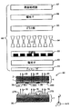
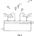
本発明の典型的実施例は添付の図面を参照しながら説明される。図2はLCDフロントエンド部品60とFEDバックライト(すなわちFEDバックライト部品)50を有する典型的なLCDディスプレイの断面を図示している。典型的実施例では、各独立したリン光体素子33は垂直のストライプ状に並ぶ、つまり図5に図示されたようなパッチを構成する。しかし本発明は、リン光体素子33が水平方向に並ぶ実施例、及び所与の色を有するリン光体が連続的に並ぶような実施例も含む。図3及び4は、本発明の典型的実施例によるFEDバックライト50の各異なる断面を図示している。図中、Y軸は垂直軸で、かつX軸は水平軸である。以降で説明するように、各独立したリン光体素子を有することで、LCD用のインテリジェントバックライトが実現可能となる。
Exemplary embodiments of the invention will now be described with reference to the accompanying drawings. FIG. 2 illustrates a cross section of a typical LCD display having an LCD
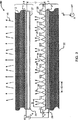
FEDバックライト50は陰極7を有する。陰極7はアレイ状に配置された複数のエミッタ16を有する。複数のエミッタ16は、陰極7内に発生する電場によって電子18を放出する。これらの電子18は陽極4へ向かって引き出される。陽極4はガラス基板2を有して良い。ガラス基板2は、その上に堆積された透明導体1を有する。各独立したリン光体素子33は透明導体1に設けられて良く、かつ互いに離れていて良い。透明導体1はインジウムスズ酸化物であって良い。リン光体素子33は、図5のように配置された、赤色リン光体(33R)、緑色リン光体(33G)、及び青色リン光体(33B)を有して良い。
The FED
FEDバックライト50の動作は、陰極7内の複数のエミッタ16からの電子18の陽極板4上のリン光体素子33への衝突、及び光子46の放出を含む。図2に表されたエミッタセルのグループ27R、27G、27Bは、各独立したリン光体素子33に対応する。ディスプレイ動作中、電位15が陽極4へ印加される。特定のアレイエミッタのアパーチャ25から電子を放出するため、ゲート電圧Vqが、誘電材料28によって支持されて良い特定のゲート26へ印加される。図3及び4に図示されているように、複数のゲート26(つまり複数のエミッタセル)は、一のリン光体素子33内で用いられて良い。
The operation of the FED
誘電材料28及び電子エミッタ16は、陰極背面29上で支持可能な陰極集合体上で支持されて良い。つまりは背面板支持構造30によって支持されているということである。
The
FEDバックライト50の輝度は、リン光体の陰極側上の薄い反射金属膜21の存在によって顕著に改善されうる。本質的には、反射金属膜21は観察者によって観察される光46を2倍にすることができる。その理由は、反射金属膜21は陰極板へ向かうように放出される光を反射し、その反射によって放出された光は陰極7から遠ざかるようにして観察者へ向かって進行するからである。
The brightness of the FED
図2は、図3-5に図示されたFED50を利用するLCDディスプレイの典型的実施例を図示している。本発明によるLCDディスプレイは一般的にディフューザ51を含むことを意図している。ディフューザ51に続き、偏光子52と回路板53が存在する。ディフューザ51及び偏光子の積層体は、たとえば3Mによって製造されているビキュティ(Vikuiti)(商標)光学膜のような、追加の輝度改善素子を有して良い。この追加の輝度改善素子は、使用されない光(たとえば偏光子によって吸収される光)をリサイクルし、かつ液晶に入射する光の角度を最適化することによって液晶ディスプレイ(LCD)の輝度を向上させる。LCDは回路板53の後に位置する液晶(LC)材料54をさらに有する。LCDディスプレイはまた、図2に図示された順序通りに、第2ガラス板55、第2偏光子56、及び表面処理膜57をも有する。図3及び4に図示された複数のエミッタ16に関しては、錐体マイクロチップエミッタとして図示されている。しかしカーボンナノチューブエミッタが好ましい。カーボンナノチューブエミッタは、1mm以上の画素解像度範囲において、10kV以上の陽極電位で動作するFEDでは有効となりうる。粗いディフューザ51を有する低解像度FEDは、LCDディスプレイ用の実質的に局所的に均一なバックライトを供する(低解像度とは、一の特定のリン光体素子、又は複数のリン光体素子からなる一の特定の繰り返しユニットが、一の特定LCD画素の専用ではないことを意味する)。本発明の特徴は、各異なるリン光体素子33からの複数の各独立した色が各独立したLCD画素を通過できるが、一のLCDセルだけ通過することである。これにより、適切なリン光体素子33が活性化され、かつその活性化されたリン光体からの光がLCD画素付近で適切に拡散するときに、白色、緑色、赤色、青色、又は上記色の組合せを供することができる。
FIG. 2 illustrates an exemplary embodiment of an LCD display utilizing the FED 50 illustrated in FIGS. 3-5. LCD displays according to the present invention are generally intended to include a
本発明の特徴は、バックライトがプログラム制御可能なFED構造であって良いことである。このような構造はインテリジェントバックライトとも呼ばれる。このことは、FEDが、スクリーン上の特定領域へ特定の色を有する光を供することができることを意味する。これは利点である。なぜなら光は、様々な液晶セル領域の活性化と不活性化によって調整されるからである。プログラム制御可能なFEDバックライトによって、LCDは、良好なブラックレベル、幅の広いダイナミックレンジ、及びぼやけのない運動の描画を実現することができる。さらに可能な限り広い色範囲を有するバックライトを供することが望ましい。これらの特性は、低解像度FEDをバックライトとして用いることによって最も簡便に実現される。FEDに含まれる発光リン光体材料は、幅広い色範囲を供するように選ばれる。 A feature of the present invention is that the backlight may have a program-controllable FED structure. Such a structure is also called an intelligent backlight. This means that the FED can provide light with a specific color to a specific area on the screen. This is an advantage. This is because light is adjusted by activation and deactivation of various liquid crystal cell regions. With a programmable FED backlight, the LCD can achieve good black level, wide dynamic range, and motion-free rendering. It is further desirable to provide a backlight having as wide a color range as possible. These characteristics are most easily realized by using a low resolution FED as a backlight. The luminescent phosphor materials included in the FED are selected to provide a wide color range.
新規の電界放出素子(FED)バックライトは驚くべきことに、LEDの全ての望ましい特性を示すにもかかわらず、かなりの低コストである。開示されたFEDがプログラム制御可能であるので、開示されたFEDはカラーフィールドシーケンス方式で動作して良い。図2に図示されたFED構造がブラックマトリックス39を有する一方で、FEDを有する市販された品質のLCDディスプレイはブラックマトリックスなしでも実現可能である(しかしブラックマトリックスは、ブラックフィールドとコントラストにおいてある程度の名目上の改善を供するが)。陰極面の適切なx-yアドレス指定によって、プログラム制御可能な冷陰極からの電子放出が可能となる。冷陰極は最も簡便にはカーボンナノチューブ(CNT)技術によって作られる。FEDの重要な利点は、陰極構造へx-yマトリックス方式で印加される電圧及び電流信号が低くても、FEDのプログラム制御が可能となることである。さらに電界放出現象が本質的に非線形であるため、x-y接合におけるスイッチとして、能動素子を組み込む必要がなくなる。FEDのさらなる利点は、放出光の電源が単純なDC電力供給であることである。放出光の電源は、この用途では10-20kV範囲で動作させることが好ましい。インテリジェントバックライト用の適切なLEDは、10-1000本の各独立してプログラム制御可能な行、及びそれとほぼ同数の列を有して良い。図5に図示された典型的FEDでは、各列は一種類のリン光体しか有しておらず、かつリン光体の色は各行に沿って循環する。この場合、系は垂直方向にプログラム制御可能であって良い。列は全体的な調節が可能である。あるいはその代わりに各行は一種類のリン光体の色を有して良い。この場合では、水平方向にプログラム制御が可能である。行は全体的な調節が可能である。本発明によるバックライトについては、各独立したリン光体素子33間での適切なピッチA(図5)が、LCDディスプレイに必要な性能の要件によって支配される。ピッチAの典型的な長さは数mm(たとえば1-5mm)であって良い。図3及び4に図示されているように、各独立したリン光体素子33は複数のエミッタセルを有して良い。各セルは、図3に図示されているように、大きさがBの開口を有するアレイのエミッタアパーチャ25を有する。適切な開口部の大きさの値Bは約10μmであって良い(図3及び4の開口部の大きさは必ずしも同一の値である必要はない)。エミッタセルのピッチDは15-30μm周辺であって良い(図3及び4のピッチの大きさDは必ずしも同一の値である必要はない)。陽極面4と陰極面7との間の間隔Cに関しては、LCDディスプレイにおけるバックライトモードのFEDについては、1mm〜数mmの間隔Cが非常に良好に機能することが分かった。好適には間隔Cは1-5mmである。このCの値は、非常に薄いディスプレイを維持することの一助となる。ピッチAが約1mmよりも広い場合には、空間電荷及びこれらの空間に関連する放出角度に起因する電子の広がりは、バックライトの色の性能に有害ではないことが分かった。換言すれば、LCDは、インテリジェントバックライトが用いられるときのバックライトの要件である比較的低い解像度を有する。そのようなものとして、陽極板と陰極板との間での電子の広がりは全く重要な問題ではない。カーボンナノチューブFEDは、発光の不均一性に起因する可視のグレインの影響を受けやすい優れた光出力を供することができる。開示された素子では、係る発光の不均一性の意図しない帰結は、FEDバックライトと液晶素子との間に適切なディフューザを用いることで取るに足らないものとなる。開示されたFEDバックライトはカラーシーケンシャルモードで動作することが好ましい。よってカラーフィルタは不要となる。しかし本発明の他の実施例には、より狭い色波長範囲を供することのできるカラーフィルタが含まれて良い。たとえば300本の各独立してアドレス指定可能な行を用いるFEDバックライトにおいては、これらの行のうちの100本を3色-赤、緑、青-の各々に割り当てることができる。それにより、任意の時点において時系列的に適切な制御信号を活性化させる際、陽極面からの赤、緑、又は青のリン光体素子のみが発光する。図5は仮想的状況のFED素子のアレイの上面図である。この図では、ある時点において、第1ブロックで表された2つの隣接する色のグループ(つまり赤33R、緑33G、青33B、及び赤33R’、緑33G’、青33B’)のうちの複数の行34中で、青のバックライトが必要とされ、かつ、続いて、第2ブロックで表された次の2つの隣接する色のグループ(つまり赤33R’’、緑33G’’、青33B’’、及び赤33R’’’、緑33G’’’、青33B’’’)うちの青のバックライトと同一の行35で、緑のバックライトが必要とされる。図5に図示された例では、列中にわずか6個のリン光体素子33しか、ある時点で活性化していない。しかしLCDは、色がLCD内のスクリーンのある特定領域で必要とされるときには、FED中の一部又は全部の列を活性化させるように設計及び動作されて良いことに留意して欲しい。本発明によるLCD部品の画素ライン数に対する各独立したリン光体素子33の各独立した行又は列の比は、1:3-1000である。好適実施例では、その比は1:100-1000である。その比が1:100-1000であることが好ましい理由は、必要とされる各独立した電気的接続数が少なくないにもかかわらず、適切なバックライトの均一性及びプログラム制御可能性が得られるためである。
The novel field emission device (FED) backlight is surprisingly low cost despite showing all the desirable properties of the LED. Since the disclosed FED is programmable, the disclosed FED may operate in a color field sequence manner. While the FED structure illustrated in FIG. 2 has a
本発明の他の態様は、FEDバックライトに用いることのできるリン光体の選択である。可能な限り最も広い広範囲を供することが望ましい。既知のFEDは、低電圧リン光体材料又はCRTリン光体材料を利用する。10-15kVの好適動作範囲では、CRTリン光体材料が最も適している。以下の表では、様々なリン光体材料とその特性が示されている。 Another aspect of the present invention is the selection of phosphors that can be used in FED backlights. It is desirable to provide the widest possible wide range. Known FEDs utilize low voltage phosphor materials or CRT phosphor materials. In the preferred operating range of 10-15 kV, CRT phosphor materials are most suitable. In the table below, various phosphor materials and their properties are shown.

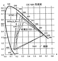
他の緑リン光体-ストロンチウムチオガレート:ユーロピウム-も特定された。図6に図示されたCIE1931色度図は、ストロンチウムチオガレート:ユーロピウムが、CRTの緑を超えてNTSCの緑に迫る色範囲を供することを示している。ストロンチウムチオガレート:ユーロピウムリン光体の負の側面は、湿気に敏感である(つまり水によって化学的に分解する)ことである。従って係るリン光体は、標準的な市販のスクリーニング技術に適用することはできない。なぜなら標準的な市販のスクリーニング技術では水を使用することが必要となるからである。そのような意味では、ストロンチウムチオガレート:ユーロピウムは考慮され得ない。 Another green phosphor-strontium thiogallate: europium-was also identified. The CIE1931 chromaticity diagram illustrated in FIG. 6 shows that strontium thiogallate: europium provides a color range that approaches the green of NTSC beyond the green of CRT. Strontium thiogallate: The negative aspect of europium phosphors is that they are sensitive to moisture (ie, chemically decomposed by water). Such phosphors are therefore not applicable to standard commercial screening techniques. This is because standard commercial screening techniques require the use of water. In that sense, strontium thiogallate: europium cannot be considered.
しかし本発明の他の態様は、水以外との相性の良いリン光体を含める手段を供する。水の相性の良くないリン光体をスクリーニングするFED用の2つの新規な静電手法が開示されている。一つは電子写真スクリーニングプロセス(EPS)で、他は直接静電スクリーニングプロセス(DES)である。 However, other embodiments of the present invention provide a means for including a phosphor that is compatible with other than water. Two novel electrostatic techniques for FED that screen for poorly water-compatible phosphors are disclosed. One is an electrophotographic screening process (EPS) and the other is a direct electrostatic screening process (DES).
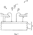
一の直接静電スクリーニングプロセス(DES)は図7を参照することで最も良く理解できる。処理は、ガラス基板上への導体の堆積で開始されて良い。図7は、ガラス基板2上に導体1を有する未完成の陽極板4を図示している。導体1は、金属(たとえばRh)の薄い層又は有機導体を堆積させることによって作られて良い。後続の処理及び/又は仕上げ後に無機導体がFED構造内部に残る場合では、その導体は透明でなければならない。有機導体の場合では、構造の処理工程において有機導体をベーキングすることができる。そのため有機導体については、透明性は必須ではない。
One direct electrostatic screening process (DES) is best understood with reference to FIG. Processing may begin with the deposition of a conductor on the glass substrate. FIG. 7 illustrates an
次に処理は、アパーチャ13を有する静電マスク12を、ガラス基板2の前方である間隔だけ離れた位置に設ける工程を有する。アパーチャ13の大きさは、ほぼリン光体ストライプの所望の大きさ(つまり図2及び5に図示された33R、33G、33Bの幅)であって良い。アパーチャ13の大きさは、リン光体ストライプの標的幅のサイズの約±20%であることが示唆される。続いて静電マスクと基板をコーティングする導体との間にバイアス電圧が印加される。そのバイアス電圧が印加される結果、図7において矢印と”E”の添え字で示された電場が生じる。チャンバ20(粒子の流束を流すための適切な配管を有する閉じた箱構造であって良い)内の荷電リン光体粒子11の流束は、基板2及び付属の静電マスク12へ向かうようにし向けられる。流束はチャンバ20へ導入され、かつその導入される位置はガラス基板と対向するマスクの面上である。リン光体粒子11は静電マスクと同一の電荷を有する。リン光体粒子11がマスクに接近するにつれて、その粒子は、周辺の電場によって、マスク12の固体表面12から飛び出してアパーチャ13を通り抜けるように案内される。それにより粒子は、アパーチャ13の下に存在する導体1の上部に堆積される。上で概説した処理工程は第1色のリン光体について行われる。異なる色である他のリン光体を塗布するため、他の静電マスク12が第1マスクに代わり、そして他の色であるリン光体粒子の次の流束を塗布するように適切に位置設定されて良い。あるいはその代わりに第1色のリン光体の堆積に用いられる既存の静電マスク12が、第2色のリン光体の標的位置内に次の色のリン光体を堆積するように適切に移動しても良い。
Next, the process includes a step of providing the
図8は別なDESの構成を図示している。図7の構成と図8の構成との基本的な差異は、基板上の導体2の上部に絶縁層3を含んでいるかいないかである。基本的には、図8に図示された構成は、図7に図示された構成と同様に機能する。ただし図8では、電荷を有して静電マスク12のアパーチャ13を通り抜けるリン光体粒子11は、絶縁体3へ堆積されても、その電荷を保持する。なぜならリン光体粒子11は、絶縁体3によって下地の導体1と隔離されているからである。絶縁体3によって、処理工程は、図7に記載されたリン光体粒子11の堆積に用いられる処理工程と同一にすることができる。
FIG. 8 illustrates another DES configuration. The fundamental difference between the configuration of FIG. 7 and the configuration of FIG. 8 is whether or not the
絶縁体3が含まれることによって、他のプリント処理も可能となる。その処理は、コロナ放電によって、静電マスク11のアパーチャ13を介して絶縁体3を帯電させる工程を有する。アパーチャ13に対して位置合わせされた絶縁体上の位置は電荷を有する。よって電荷を有するリン光体粒子11は、チャンバ内へ導入が可能で、かつリン光体粒子11とは反対の電荷を有する導体の上へ堆積する。
By including the
絶縁体3を含めることは、固定工程にも有利に利用することができる。図9の画は、絶縁体と固定工程を有する実施例による処理に係る様々な段階を図示している。図9Aは3種類のリン光体の堆積及び静電マスクの除去が行われた後の陽極板4のプロファイルを図示している。図9Bは固定工程の結果を図示している。その固定は、絶縁体を部分的に溶解する溶媒を適用することによって行われて良い。それにより、リン光体粒子を絶縁体3へ浸漬させ、かつ毛管作用によって絶縁材料の一部をリン光体へ入り込ませることが可能となる。溶媒が蒸発した結果、リン光体堆積物は陽極板4に強く固着する。固定工程は、膜生成工程中でのリン光体粒子の意図しない運動を防止することの一助となる。好適実施例では、絶縁体は厚さが約5-10μmのポリスチレン材料で、かつ、リン光体の固定は陽極板に溶媒を噴霧することによって実現される。固定工程に続き、ラッカー膜5の層が陽極板上に成膜されて良い。その後図9Cに図示されているように、反射金属膜21が成膜される。ベーキング工程後、ブラックマトリックス39が用いられない場合の陽極板4の最終構造が図4Dに図示されている。ブラックマトリックス39が用いられる場合、ブラックマトリックス39は反射金属膜21の成膜前に成膜され、かつ、スクリーン構造は図2に図示された構造に似るだろう。
Inclusion of the
あるいはその代わりに、リン光体素子は、電子写真スクリーニング(EPS)プロセスによって堆積されても良い。EPSは概略的には図10に図示されている。そのプロセスは、図10Aに図示されているように有機導体膜41の成膜によって開始される。その後図10Bに図示されているように、有機光伝導体膜42が成膜される。続いて図10Cに図示されているように、有機光伝導体膜42は、好適にはコロナ放電体によって、帯電する。その後マスク43がスクリーンによって位置設定される。マスク43は、リン光体素子の好適位置に対応するアパーチャを有する。続いて図10Dに図示されているように、有機光伝導体は、マスク43のアパーチャを通過する光に露光される。その光に露光された有機光伝導体の領域の電荷は放出され、露光されていない領域は帯電したままである。図10Eに図示されているように、チャンバ20(粒子の流束を流すための適切な配管を有する閉じた箱構造であって良い)内での帯電したリン光体粒子11の流束は基板へ向かって流れるようにし向けられ、かつ、帯電したリン光粒子11は電荷を放出した有機光伝導体の領域上へ堆積する。(あるいはその代わりに、リン光体の現像は、有機光伝導体の適切に帯電した位置への反対電荷が帯電したリン光体を堆積させる工程を有して良い。)図10Cに図示されているコロナ放電工程、図10Dに図示されている露光と電荷放出工程、及び帯電したリン光体粒子11の堆積による現像工程は、追加のリン光体の色を堆積するために繰り返されて良い。必要な色のリン光体全てが陽極板4に堆積されるとき、その陽極板は図10Fに図示されているように固定されて膜を形成して良い。膜の形成に続いて、反射金属膜が陽極板に成膜されて良く、かつ、その陽極板は陰極板7と組み合わせられることで、FED素子が完成する。FEDの完成後、そのFEDはLCDの背面と接合することで、LCD用のバックライトを供する。本明細書に開示された処理に従って作製されたそのFED素子はまた、液晶フロントエンド部品は含まれない直接ディスプレイ素子として用いるためにも作製されて良い。
Alternatively, the phosphor element may be deposited by an electrophotographic screening (EPS) process. The EPS is schematically illustrated in FIG. The process is started by forming the
Claims (13)
低解像度の電界放出型バックライト部品;
を有する液晶ディスプレイであって、
前記電界放出型バックライト部品は、低解像度で、かつ、前記第1方向に特定のリン光体素子の列を有し、
前記電界放出型バックライト部品の列の特定のリン光体素子は、前記液晶フロントエンド部品の特定の画素のラインに限定されない、
液晶ディスプレイ。LCD front-end components with pixel lines in the first direction ; and low-resolution field emission backlight components;
A liquid crystal display having
The field emission backlight component has a low resolution and a specific row of phosphor elements in the first direction,
The specific phosphor elements in the column of field emission backlight components are not limited to specific pixel lines of the liquid crystal front end components,
LCD display.
該繰り返しユニット中の各独立したリン光体素子の色はそれぞれ異なっている、
請求項2に記載の液晶ディスプレイ。The plurality of independent phosphor elements are grouped into repeating units, and the colors of the individual phosphor elements in the repeating unit are different from each other;
3. A liquid crystal display according to claim 2.
選択されたグループを構成する各独立した素子が、前記液晶フロントエンド部品の関連する液晶セルの起動と連動して起動するように、
プログラム制御可能で、かつ同期がとられる、
請求項2又は3に記載の液晶ディスプレイ。Each independent element of the field emission backlight component is:
Each independent element constituting the selected group is activated in conjunction with activation of an associated liquid crystal cell of the liquid crystal front end component,
Programmable and synchronized
The liquid crystal display according to claim 2 or 3.
Applications Claiming Priority (3)
| Application Number | Priority Date | Filing Date | Title |
|---|---|---|---|
| US81724106P | 2006-06-28 | 2006-06-28 | |
| US60/817,241 | 2006-06-28 | ||
| PCT/US2006/038827 WO2008002320A1 (en) | 2006-06-28 | 2006-10-04 | Liquid crystal display having a field emission backlight |
Publications (3)
| Publication Number | Publication Date |
|---|---|
| JP2009543291A JP2009543291A (en) | 2009-12-03 |
| JP2009543291A5 JP2009543291A5 (en) | 2010-01-21 |
| JP5153772B2 true JP5153772B2 (en) | 2013-02-27 |
Family
ID=37560940
Family Applications (2)
| Application Number | Title | Priority Date | Filing Date |
|---|---|---|---|
| JP2009518089A Active JP5117492B2 (en) | 2006-06-28 | 2006-10-04 | Liquid crystal display with field emission backlight |
| JP2009518088A Active JP5153772B2 (en) | 2006-06-28 | 2006-10-04 | Liquid crystal display with field emission backlight |
Family Applications Before (1)
| Application Number | Title | Priority Date | Filing Date |
|---|---|---|---|
| JP2009518089A Active JP5117492B2 (en) | 2006-06-28 | 2006-10-04 | Liquid crystal display with field emission backlight |
Country Status (6)
| Country | Link |
|---|---|
| US (2) | US9111742B2 (en) |
| EP (2) | EP2038909B1 (en) |
| JP (2) | JP5117492B2 (en) |
| KR (2) | KR101299035B1 (en) |
| CN (2) | CN101473399B (en) |
| WO (2) | WO2008002321A1 (en) |
Families Citing this family (13)
| Publication number | Priority date | Publication date | Assignee | Title |
|---|---|---|---|---|
| US9111742B2 (en) | 2006-06-28 | 2015-08-18 | Thomson Licensing | Liquid crystal display having a field emission backlight |
| WO2008033502A2 (en) * | 2006-09-15 | 2008-03-20 | Thomson Licensing | Display utilizing simultaneous color intelligent backlighting and luminescence controlling shutters |
| JP5216780B2 (en) * | 2006-12-18 | 2013-06-19 | トムソン ライセンシング | Display device having field emission portion with black matrix |
| KR101404846B1 (en) * | 2006-12-18 | 2014-06-09 | 톰슨 라이센싱 | Screen structure for field emission device backlighting unit |
| KR20090015748A (en) * | 2007-08-09 | 2009-02-12 | 삼성모바일디스플레이주식회사 | Blacklight unit and image display apparatus employing the same |
| KR20090076551A (en) * | 2008-01-09 | 2009-07-13 | 삼성에스디아이 주식회사 | Display device |
| US9529228B2 (en) | 2010-11-05 | 2016-12-27 | Yissum Research Development Company Of The Hebrew University Of Jerusalem, Ltd. | Polarizing lighting systems |
| CN102929039B (en) * | 2012-11-05 | 2015-06-03 | 福州大学 | Liquid crystal display-field emission display (LCD-FED) double-screen structure high-dynamic display system |
| US9171509B2 (en) | 2013-04-19 | 2015-10-27 | VIZIO Inc. | Single backlight source where the backlight emits pure colored light in a sequential manner where the sequence is red, blue and green |
| US20170005116A1 (en) * | 2015-07-01 | 2017-01-05 | Apple Inc. | Displays Having Substrate Ledge Support |
| CN109493809B (en) * | 2017-09-12 | 2021-01-01 | 纬创资通(中山)有限公司 | Display device and backlight driving method |
| CN109238388B (en) * | 2018-09-21 | 2024-01-05 | 新开普电子股份有限公司 | LCD display of gas meter |
| CN109188770B (en) * | 2018-10-12 | 2021-07-23 | 江西省弘叶光电科技有限公司 | Backlight source module and liquid crystal display thereof |
Family Cites Families (86)
| Publication number | Priority date | Publication date | Assignee | Title |
|---|---|---|---|---|
| NL195682A (en) | 1954-03-24 | |||
| US3479711A (en) * | 1966-08-25 | 1969-11-25 | Hughes Aircraft Co | Method and apparatus for producing a color kinescope and blank unit therefor |
| JPS58189943A (en) | 1982-04-30 | 1983-11-05 | Hitachi Ltd | Forming method of coated layer with pulverulent body |
| FI73325C (en) | 1985-03-05 | 1987-09-10 | Elkoteade Ag | FOERFARANDE FOER ALSTRING AV INDIVIDUELLT REGLERBARA BILDELEMENT OCH PAO DESSA BASERAD FAERGDISPLAY. |
| EP0324147A3 (en) | 1988-01-11 | 1990-07-04 | Seiko Epson Corporation | Light guide type display apparatus |
| JP2582644B2 (en) | 1989-08-10 | 1997-02-19 | 富士写真フイルム株式会社 | Flat panel image display |
| US5347201A (en) | 1991-02-25 | 1994-09-13 | Panocorp Display Systems | Display device |
| US5319282A (en) | 1991-12-30 | 1994-06-07 | Winsor Mark D | Planar fluorescent and electroluminescent lamp having one or more chambers |
| EP0623944B1 (en) * | 1993-05-05 | 1997-07-02 | AT&T Corp. | Flat panel display apparatus, and method of making same |
| US5831387A (en) | 1994-05-20 | 1998-11-03 | Canon Kabushiki Kaisha | Image forming apparatus and a method for manufacturing the same |
| US6573961B2 (en) | 1994-06-27 | 2003-06-03 | Reveo, Inc. | High-brightness color liquid crystal display panel employing light recycling therein |
| US6252569B1 (en) | 1994-09-28 | 2001-06-26 | Texas Instruments Incorporated | Large field emission display (FED) made up of independently operated display sections integrated behind one common continuous large anode which displays one large image or multiple independent images |
| US6184969B1 (en) | 1994-10-25 | 2001-02-06 | James L. Fergason | Optical display system and method, active and passive dithering using birefringence, color image superpositioning and display enhancement |
| US5646702A (en) | 1994-10-31 | 1997-07-08 | Honeywell Inc. | Field emitter liquid crystal display |
| US5866039A (en) | 1995-01-13 | 1999-02-02 | The United States Of America As Represented By The Secretary Of The Army | Luminescent device for displays and lighting |
| US5760858A (en) | 1995-04-21 | 1998-06-02 | Texas Instruments Incorporated | Field emission device panel backlight for liquid crystal displays |
| US5554468A (en) | 1995-04-27 | 1996-09-10 | Thomson Consumer Electronics, Inc. | CRT electrophotographic screening method using an organic photoconductive layer |
| US5611719A (en) | 1995-07-06 | 1997-03-18 | Texas Instruments Incorporated | Method for improving flat panel display anode plate phosphor efficiency |
| US20020115269A1 (en) * | 1995-07-11 | 2002-08-22 | Applied Materials, Inc. | Method of depositing amorphous silicon based films having controlled conductivity |
| US5772488A (en) | 1995-10-16 | 1998-06-30 | Micron Display Technology, Inc. | Method of forming a doped field emitter array |
| JPH09199028A (en) | 1995-12-15 | 1997-07-31 | Thomson Consumer Electron Inc | Method for manufacturing luminescent screen assembly for cathode-ray tube electrophotographically |
| US5926239A (en) * | 1996-08-16 | 1999-07-20 | Si Diamond Technology, Inc. | Backlights for color liquid crystal displays |
| JP3171121B2 (en) | 1996-08-29 | 2001-05-28 | 双葉電子工業株式会社 | Field emission display |
| KR100286828B1 (en) | 1996-09-18 | 2001-04-16 | 니시무로 타이죠 | Flat panel display device |
| JPH10134717A (en) | 1996-10-29 | 1998-05-22 | Matsushita Electric Ind Co Ltd | Manufacture of plasma display panel |
| KR19980038178A (en) * | 1996-11-25 | 1998-08-05 | 손욱 | Method for manufacturing fluorescent film of cathode ray tube |
| US5827624A (en) | 1996-12-30 | 1998-10-27 | Micron Display Technology, Inc. | Mask modification for focal plane on contact photolithography tool |
| US7625420B1 (en) | 1997-02-24 | 2009-12-01 | Cabot Corporation | Copper powders methods for producing powders and devices fabricated from same |
| US6197218B1 (en) | 1997-02-24 | 2001-03-06 | Superior Micropowders Llc | Photoluminescent phosphor powders, methods for making phosphor powders and devices incorporating same |
| US6875372B1 (en) | 1997-02-24 | 2005-04-05 | Cabot Corporation | Cathodoluminescent phosphor powders, methods for making phosphor powders and devices incorporating same |
| JP3247643B2 (en) | 1997-09-10 | 2002-01-21 | インターナショナル・ビジネス・マシーンズ・コーポレーション | Liquid crystal display device |
| CN2309577Y (en) | 1997-10-10 | 1999-03-03 | 邹德春 | Synchronous scanning liquid crystal display screen rear light source |
| JP3328198B2 (en) | 1998-08-17 | 2002-09-24 | 日本電気株式会社 | Liquid crystal display |
| US6300021B1 (en) | 1999-06-14 | 2001-10-09 | Thomson Licensing S.A. | Bias shield and method of developing a latent charge image |
| KR100476043B1 (en) | 1999-06-21 | 2005-03-10 | 비오이 하이디스 테크놀로지 주식회사 | FED device and method for manufacturing the same |
| KR100589398B1 (en) | 1999-08-20 | 2006-06-13 | 삼성에스디아이 주식회사 | Flat panel display |
| US6448709B1 (en) | 1999-09-15 | 2002-09-10 | Industrial Technology Research Institute | Field emission display panel having diode structure and method for fabricating |
| US6353286B1 (en) | 1999-10-08 | 2002-03-05 | Motorola, Inc | Field emission display having a multi-layered barrier structure |
| US6570322B1 (en) * | 1999-11-09 | 2003-05-27 | Micron Technology, Inc. | Anode screen for a phosphor display with a plurality of pixel regions defining phosphor layer holes |
| JP4355977B2 (en) | 1999-11-12 | 2009-11-04 | ソニー株式会社 | Image display device and illumination control method in image display device |
| US6426590B1 (en) | 2000-01-13 | 2002-07-30 | Industrial Technology Research Institute | Planar color lamp with nanotube emitters and method for fabricating |
| JP2001222967A (en) | 2000-02-07 | 2001-08-17 | Sony Corp | Field-emission display device and its manufacturing method |
| JP3999922B2 (en) | 2000-03-29 | 2007-10-31 | 京セラ株式会社 | Protruded substrate and flat display |
| KR100366704B1 (en) | 2000-04-27 | 2003-01-09 | 삼성에스디아이 주식회사 | Liquid crystal display device |
| JP2002124180A (en) | 2000-10-18 | 2002-04-26 | Canon Inc | Manufacturing method of electron-emitting element, electron-emitting element, electron source and image forming device |
| US6734469B2 (en) | 2000-11-17 | 2004-05-11 | Tdk Corporation | EL phosphor laminate thin film and EL device |
| JP4027602B2 (en) | 2001-01-12 | 2007-12-26 | 株式会社リコー | Development device and image forming device |
| EP2309314B1 (en) | 2001-02-27 | 2020-12-16 | Dolby Laboratories Licensing Corporation | A method and device for displaying an image |
| US7184066B2 (en) | 2001-05-09 | 2007-02-27 | Clairvoyante, Inc | Methods and systems for sub-pixel rendering with adaptive filtering |
| JP3918472B2 (en) | 2001-08-01 | 2007-05-23 | セイコーエプソン株式会社 | Electro-optical device and electronic apparatus |
| US6690349B2 (en) | 2001-11-09 | 2004-02-10 | Koninklijke Philips Electronics N.V. | Scrolling backlight system for LCD TV |
| US7064740B2 (en) | 2001-11-09 | 2006-06-20 | Sharp Laboratories Of America, Inc. | Backlit display with improved dynamic range |
| US7583279B2 (en) | 2004-04-09 | 2009-09-01 | Samsung Electronics Co., Ltd. | Subpixel layouts and arrangements for high brightness displays |
| JP2003242885A (en) | 2002-02-19 | 2003-08-29 | Dainippon Printing Co Ltd | Manufacturing method of substrate for field emission type display |
| JP3636154B2 (en) | 2002-03-27 | 2005-04-06 | ソニー株式会社 | Cold cathode field emission device and manufacturing method thereof, cold cathode field electron emission display device and manufacturing method thereof |
| KR20030092730A (en) | 2002-05-31 | 2003-12-06 | 엘지.필립스디스플레이(주) | Flat panel display |
| US6950088B2 (en) | 2002-06-17 | 2005-09-27 | Koninklijke Philips Electronics N.V. | Synchronizing optical scan and electrical addressing of a single-panel, scrolling color LCD system |
| JP3373507B1 (en) | 2002-07-16 | 2003-02-04 | パイオニア株式会社 | Surface discharge type plasma display device |
| US7176878B2 (en) | 2002-12-11 | 2007-02-13 | Nvidia Corporation | Backlight dimming and LCD amplitude boost |
| KR100502821B1 (en) * | 2002-12-26 | 2005-07-22 | 이호영 | Low temperature formation method for emitter tip including copper oxide nanowire or copper nanowire and display device or light source having emitter tip manufactured by using the same method |
| JP4120414B2 (en) | 2003-02-07 | 2008-07-16 | 三菱電機株式会社 | Projection display apparatus and image signal conversion method |
| KR100918280B1 (en) | 2003-02-17 | 2009-09-18 | 엘지디스플레이 주식회사 | liquid crystal display device module |
| US7293591B2 (en) * | 2003-02-28 | 2007-11-13 | Ishida Co., Ltd. | System for mounting products to a tape |
| US7046262B2 (en) | 2003-03-31 | 2006-05-16 | Sharp Laboratories Of America, Inc. | System for displaying images on a display |
| US7157848B2 (en) | 2003-06-06 | 2007-01-02 | Electrovac Fabrikation Elektrotechnischer Spezialartikel Gmbh | Field emission backlight for liquid crystal television |
| JP4304125B2 (en) | 2003-10-03 | 2009-07-29 | 日本碍子株式会社 | Electron emitter |
| KR101002278B1 (en) | 2004-02-03 | 2010-12-20 | 삼성에스디아이 주식회사 | Field emission type backlight device |
| JP4628770B2 (en) | 2004-02-09 | 2011-02-09 | 株式会社日立製作所 | Image display device having illumination device and image display method |
| US7239080B2 (en) | 2004-03-11 | 2007-07-03 | Avago Technologies Ecbu Ip (Singapore) Pte. Ltd | LED display with overlay |
| ES2391095T3 (en) | 2004-05-03 | 2012-11-21 | Dolby Laboratories Licensing Corporation | Procedure for efficient computation of image frames, for dual modulation display systems, using key frames |
| US7872631B2 (en) | 2004-05-04 | 2011-01-18 | Sharp Laboratories Of America, Inc. | Liquid crystal display with temporal black point |
| US7532192B2 (en) | 2004-05-04 | 2009-05-12 | Sharp Laboratories Of America, Inc. | Liquid crystal display with filtered black point |
| US7612757B2 (en) | 2004-05-04 | 2009-11-03 | Sharp Laboratories Of America, Inc. | Liquid crystal display with modulated black point |
| KR101016288B1 (en) | 2004-06-29 | 2011-02-22 | 엘지디스플레이 주식회사 | liquid crystal display device and method for driving the same |
| US7511415B2 (en) * | 2004-08-26 | 2009-03-31 | Dialight Japan Co., Ltd. | Backlight for liquid crystal display device |
| DE112005002127T5 (en) | 2004-09-03 | 2007-10-04 | Sumitomo Electric Industries, Ltd. | Phosphor, process for producing the same, and light-emitting device using the same |
| CN1770352A (en) * | 2004-11-05 | 2006-05-10 | 清华大学 | Field emission device and field emission display equipped with the same |
| JP2006154235A (en) | 2004-11-29 | 2006-06-15 | Sharp Corp | Developing device and image forming apparatus |
| JP2006156377A (en) | 2004-12-01 | 2006-06-15 | Nanopacific Inc | Field emission device driven by bipolar pulse power supply |
| US7782405B2 (en) | 2004-12-02 | 2010-08-24 | Sharp Laboratories Of America, Inc. | Systems and methods for selecting a display source light illumination level |
| KR20070003467A (en) | 2005-07-02 | 2007-01-05 | 삼성전자주식회사 | Surface light source device and liquid crystal display having the same |
| US20070024772A1 (en) | 2005-07-28 | 2007-02-01 | Childers Winthrop D | Display with sub-region backlighting |
| CN101473397A (en) * | 2006-06-23 | 2009-07-01 | 汤姆森许可贸易公司 | Luminescent material for carbon nanotube (CNT)/field emission device (FED) display |
| US9111742B2 (en) * | 2006-06-28 | 2015-08-18 | Thomson Licensing | Liquid crystal display having a field emission backlight |
| KR101404846B1 (en) | 2006-12-18 | 2014-06-09 | 톰슨 라이센싱 | Screen structure for field emission device backlighting unit |
| JP5216780B2 (en) * | 2006-12-18 | 2013-06-19 | トムソン ライセンシング | Display device having field emission portion with black matrix |
-
2006
- 2006-10-04 US US12/308,816 patent/US9111742B2/en active Active
- 2006-10-04 US US12/308,906 patent/US8259258B2/en active Active
- 2006-10-04 KR KR1020087031589A patent/KR101299035B1/en active IP Right Grant
- 2006-10-04 CN CN2006800551493A patent/CN101473399B/en active Active
- 2006-10-04 JP JP2009518089A patent/JP5117492B2/en active Active
- 2006-10-04 EP EP06816304.7A patent/EP2038909B1/en active Active
- 2006-10-04 WO PCT/US2006/038938 patent/WO2008002321A1/en active Application Filing
- 2006-10-04 CN CN200680055173.7A patent/CN101479653B/en active Active
- 2006-10-04 EP EP06816234.6A patent/EP2038699B1/en active Active
- 2006-10-04 KR KR1020087031582A patent/KR101210530B1/en active IP Right Grant
- 2006-10-04 WO PCT/US2006/038827 patent/WO2008002320A1/en active Application Filing
- 2006-10-04 JP JP2009518088A patent/JP5153772B2/en active Active
Also Published As
| Publication number | Publication date |
|---|---|
| US8259258B2 (en) | 2012-09-04 |
| US9111742B2 (en) | 2015-08-18 |
| KR101299035B1 (en) | 2013-08-27 |
| KR101210530B1 (en) | 2012-12-10 |
| EP2038699A1 (en) | 2009-03-25 |
| US20090185110A1 (en) | 2009-07-23 |
| CN101473399A (en) | 2009-07-01 |
| JP2009543291A (en) | 2009-12-03 |
| JP5117492B2 (en) | 2013-01-16 |
| WO2008002321A1 (en) | 2008-01-03 |
| CN101479653A (en) | 2009-07-08 |
| CN101479653B (en) | 2012-10-03 |
| EP2038699B1 (en) | 2013-08-07 |
| WO2008002320A1 (en) | 2008-01-03 |
| JP2009543292A (en) | 2009-12-03 |
| US20090186165A1 (en) | 2009-07-23 |
| EP2038909B1 (en) | 2013-08-14 |
| CN101473399B (en) | 2011-03-23 |
| KR20090028560A (en) | 2009-03-18 |
| KR20090028558A (en) | 2009-03-18 |
| EP2038909A1 (en) | 2009-03-25 |
Similar Documents
| Publication | Publication Date | Title |
|---|---|---|
| JP5153772B2 (en) | Liquid crystal display with field emission backlight | |
| US6545422B1 (en) | Socket for use with a micro-component in a light-emitting panel | |
| TWI436130B (en) | A liquid crystal display | |
| CN1471702A (en) | A method for testinga light-emtiting panel and the components therein | |
| CN1471699A (en) | A method and system for energizing a micro-component in a light-emitting panel | |
| US20100045589A1 (en) | Display device having field emission unit with black matrix | |
| US7701127B2 (en) | Field emission backlight unit | |
| JP2009543118A (en) | Luminescent display device having filter material | |
| US20050280366A1 (en) | Double-faced plasma display panel | |
| CN100385604C (en) | Electron emission device and method of manufacturing the same | |
| KR940004241B1 (en) | Liquid crystal display devices of method of plasma address | |
| KR100255451B1 (en) | Plasma display panel and manufacturing method thereof | |
| JPS6286651A (en) | Fluorescent luminous tube | |
| JP2003203558A (en) | Method of manufacturing display device and display device | |
| KR20030072970A (en) | Plasma display panel | |
| KR19980087878A (en) | Fluorescent wire and manufacturing method thereof and color display device using same |
Legal Events
| Date | Code | Title | Description |
|---|---|---|---|
| A521 | Request for written amendment filed |
Free format text: JAPANESE INTERMEDIATE CODE: A523 Effective date: 20091001 |
|
| A621 | Written request for application examination |
Free format text: JAPANESE INTERMEDIATE CODE: A621 Effective date: 20091001 |
|
| A977 | Report on retrieval |
Free format text: JAPANESE INTERMEDIATE CODE: A971007 Effective date: 20111027 |
|
| A131 | Notification of reasons for refusal |
Free format text: JAPANESE INTERMEDIATE CODE: A131 Effective date: 20111108 |
|
| A601 | Written request for extension of time |
Free format text: JAPANESE INTERMEDIATE CODE: A601 Effective date: 20120207 |
|
| A602 | Written permission of extension of time |
Free format text: JAPANESE INTERMEDIATE CODE: A602 Effective date: 20120214 |
|
| A521 | Request for written amendment filed |
Free format text: JAPANESE INTERMEDIATE CODE: A523 Effective date: 20120507 |
|
| TRDD | Decision of grant or rejection written | ||
| A01 | Written decision to grant a patent or to grant a registration (utility model) |
Free format text: JAPANESE INTERMEDIATE CODE: A01 Effective date: 20121106 |
|
| A61 | First payment of annual fees (during grant procedure) |
Free format text: JAPANESE INTERMEDIATE CODE: A61 Effective date: 20121204 |
|
| FPAY | Renewal fee payment (event date is renewal date of database) |
Free format text: PAYMENT UNTIL: 20151214 Year of fee payment: 3 |
|
| R150 | Certificate of patent or registration of utility model |
Ref document number: 5153772 Country of ref document: JP Free format text: JAPANESE INTERMEDIATE CODE: R150 Free format text: JAPANESE INTERMEDIATE CODE: R150 |
|
| R250 | Receipt of annual fees |
Free format text: JAPANESE INTERMEDIATE CODE: R250 |
|
| S111 | Request for change of ownership or part of ownership |
Free format text: JAPANESE INTERMEDIATE CODE: R313113 |
|
| S531 | Written request for registration of change of domicile |
Free format text: JAPANESE INTERMEDIATE CODE: R313531 |
|
| R360 | Written notification for declining of transfer of rights |
Free format text: JAPANESE INTERMEDIATE CODE: R360 |
|
| R360 | Written notification for declining of transfer of rights |
Free format text: JAPANESE INTERMEDIATE CODE: R360 |
|
| R371 | Transfer withdrawn |
Free format text: JAPANESE INTERMEDIATE CODE: R371 |
|
| S531 | Written request for registration of change of domicile |
Free format text: JAPANESE INTERMEDIATE CODE: R313531 |
|
| R350 | Written notification of registration of transfer |
Free format text: JAPANESE INTERMEDIATE CODE: R350 |
|
| R250 | Receipt of annual fees |
Free format text: JAPANESE INTERMEDIATE CODE: R250 |
|
| S111 | Request for change of ownership or part of ownership |
Free format text: JAPANESE INTERMEDIATE CODE: R313113 |
|
| R350 | Written notification of registration of transfer |
Free format text: JAPANESE INTERMEDIATE CODE: R350 |
|
| R250 | Receipt of annual fees |
Free format text: JAPANESE INTERMEDIATE CODE: R250 |
|
| R250 | Receipt of annual fees |
Free format text: JAPANESE INTERMEDIATE CODE: R250 |
|
| R250 | Receipt of annual fees |
Free format text: JAPANESE INTERMEDIATE CODE: R250 |