JP5145359B2 - Optical storage medium having mask layer providing super-resolution near-field effect, and each manufacturing method - Google Patents
Optical storage medium having mask layer providing super-resolution near-field effect, and each manufacturing method Download PDFInfo
- Publication number
- JP5145359B2 JP5145359B2 JP2009546723A JP2009546723A JP5145359B2 JP 5145359 B2 JP5145359 B2 JP 5145359B2 JP 2009546723 A JP2009546723 A JP 2009546723A JP 2009546723 A JP2009546723 A JP 2009546723A JP 5145359 B2 JP5145359 B2 JP 5145359B2
- Authority
- JP
- Japan
- Prior art keywords
- layer
- storage medium
- optical storage
- data
- nanometers
- Prior art date
- Legal status (The legal status is an assumption and is not a legal conclusion. Google has not performed a legal analysis and makes no representation as to the accuracy of the status listed.)
- Expired - Fee Related
Links
- 230000003287 optical effect Effects 0.000 title claims abstract description 49
- 230000000694 effects Effects 0.000 title claims description 9
- 238000004519 manufacturing process Methods 0.000 title abstract description 4
- 239000002105 nanoparticle Substances 0.000 claims abstract description 38
- 239000000758 substrate Substances 0.000 claims abstract description 11
- 238000004528 spin coating Methods 0.000 claims abstract description 9
- 238000000034 method Methods 0.000 claims description 5
- 229910052751 metal Inorganic materials 0.000 claims description 4
- 239000002184 metal Substances 0.000 claims description 4
- 229910000510 noble metal Inorganic materials 0.000 claims 1
- 230000005669 field effect Effects 0.000 abstract 1
- 239000010410 layer Substances 0.000 description 131
- 239000000463 material Substances 0.000 description 8
- 238000004544 sputter deposition Methods 0.000 description 6
- FOIXSVOLVBLSDH-UHFFFAOYSA-N Silver ion Chemical compound [Ag+] FOIXSVOLVBLSDH-UHFFFAOYSA-N 0.000 description 3
- 229910000618 GeSbTe Inorganic materials 0.000 description 2
- 229910004298 SiO 2 Inorganic materials 0.000 description 2
- 239000003989 dielectric material Substances 0.000 description 2
- 230000003993 interaction Effects 0.000 description 2
- 229910044991 metal oxide Inorganic materials 0.000 description 2
- 150000004706 metal oxides Chemical class 0.000 description 2
- BASFCYQUMIYNBI-UHFFFAOYSA-N platinum Chemical compound [Pt] BASFCYQUMIYNBI-UHFFFAOYSA-N 0.000 description 2
- 229910000763 AgInSbTe Inorganic materials 0.000 description 1
- 229910052782 aluminium Inorganic materials 0.000 description 1
- XAGFODPZIPBFFR-UHFFFAOYSA-N aluminium Chemical compound [Al] XAGFODPZIPBFFR-UHFFFAOYSA-N 0.000 description 1
- 150000001875 compounds Chemical class 0.000 description 1
- 239000002355 dual-layer Substances 0.000 description 1
- 238000005516 engineering process Methods 0.000 description 1
- 239000002082 metal nanoparticle Substances 0.000 description 1
- 239000012782 phase change material Substances 0.000 description 1
- 229910052697 platinum Inorganic materials 0.000 description 1
- 239000011241 protective layer Substances 0.000 description 1
- 238000005546 reactive sputtering Methods 0.000 description 1
Images


Classifications
-
- G—PHYSICS
- G11—INFORMATION STORAGE
- G11B—INFORMATION STORAGE BASED ON RELATIVE MOVEMENT BETWEEN RECORD CARRIER AND TRANSDUCER
- G11B7/00—Recording or reproducing by optical means, e.g. recording using a thermal beam of optical radiation by modifying optical properties or the physical structure, reproducing using an optical beam at lower power by sensing optical properties; Record carriers therefor
- G11B7/24—Record carriers characterised by shape, structure or physical properties, or by the selection of the material
- G11B7/241—Record carriers characterised by shape, structure or physical properties, or by the selection of the material characterised by the selection of the material
- G11B7/252—Record carriers characterised by shape, structure or physical properties, or by the selection of the material characterised by the selection of the material of layers other than recording layers
- G11B7/257—Record carriers characterised by shape, structure or physical properties, or by the selection of the material characterised by the selection of the material of layers other than recording layers of layers having properties involved in recording or reproduction, e.g. optical interference layers or sensitising layers or dielectric layers, which are protecting the recording layers
-
- B—PERFORMING OPERATIONS; TRANSPORTING
- B82—NANOTECHNOLOGY
- B82Y—SPECIFIC USES OR APPLICATIONS OF NANOSTRUCTURES; MEASUREMENT OR ANALYSIS OF NANOSTRUCTURES; MANUFACTURE OR TREATMENT OF NANOSTRUCTURES
- B82Y10/00—Nanotechnology for information processing, storage or transmission, e.g. quantum computing or single electron logic
-
- G—PHYSICS
- G11—INFORMATION STORAGE
- G11B—INFORMATION STORAGE BASED ON RELATIVE MOVEMENT BETWEEN RECORD CARRIER AND TRANSDUCER
- G11B7/00—Recording or reproducing by optical means, e.g. recording using a thermal beam of optical radiation by modifying optical properties or the physical structure, reproducing using an optical beam at lower power by sensing optical properties; Record carriers therefor
- G11B7/24—Record carriers characterised by shape, structure or physical properties, or by the selection of the material
- G11B7/2403—Layers; Shape, structure or physical properties thereof
- G11B7/24056—Light transmission layers lying on the light entrance side and being thinner than the substrate, e.g. specially adapted for Blu-ray® discs
- G11B7/24059—Light transmission layers lying on the light entrance side and being thinner than the substrate, e.g. specially adapted for Blu-ray® discs specially adapted for near-field recording or reproduction
-
- Y—GENERAL TAGGING OF NEW TECHNOLOGICAL DEVELOPMENTS; GENERAL TAGGING OF CROSS-SECTIONAL TECHNOLOGIES SPANNING OVER SEVERAL SECTIONS OF THE IPC; TECHNICAL SUBJECTS COVERED BY FORMER USPC CROSS-REFERENCE ART COLLECTIONS [XRACs] AND DIGESTS
- Y10—TECHNICAL SUBJECTS COVERED BY FORMER USPC
- Y10T—TECHNICAL SUBJECTS COVERED BY FORMER US CLASSIFICATION
- Y10T428/00—Stock material or miscellaneous articles
- Y10T428/21—Circular sheet or circular blank
Landscapes
- Engineering & Computer Science (AREA)
- Chemical & Material Sciences (AREA)
- Nanotechnology (AREA)
- Physics & Mathematics (AREA)
- Mathematical Physics (AREA)
- Theoretical Computer Science (AREA)
- Crystallography & Structural Chemistry (AREA)
- Optical Record Carriers And Manufacture Thereof (AREA)
- Optical Recording Or Reproduction (AREA)
- Manufacturing Optical Record Carriers (AREA)
Abstract
Description
本発明は光学記憶媒体に関し、特に、超解像近接場効果を用いて高データ密度で読取専用領域にデータを格納する光学ディスク、および各光学記憶媒体を製造する方法に関する。 The present invention relates to an optical storage medium, and more particularly, to an optical disk that stores data in a read-only area at a high data density using the super-resolution near-field effect, and a method of manufacturing each optical storage medium.
光学記憶媒体は、光学的に読み取り可能な方法でデータが格納される媒体であり、例えば、ピックアップに統合されたレーザーおよび光検出器によりなされる。この光検出器は、データを読み取るときに、レーザービームの反射光を検出するために用いられる。一方、多くの様々な光学記憶媒体が知られており、異なるレーザー波長で動作するものや、1ギガバイトから50ギガバイト(GB)までの記憶容量を備える異なるサイズのものなどである。このフォーマットは、オーディオCDやビデオDVDなどの読み取り専用フォーマットと、CD−R、DVD−R、DVD+Rなどのライトワンス(write-once)およびCD−RW、DVD−RW、DVD+RWのようなリライタブル(rewritable)フォーマットの光学媒体と、を含む。デジタルデータは、この媒体の1またはそれ以上の層の中のトラックに沿ってこれら媒体上に格納される。 An optical storage medium is a medium in which data is stored in an optically readable manner, for example, by a laser and a photodetector integrated in a pickup. This photodetector is used to detect the reflected light of the laser beam when reading data. On the other hand, many different optical storage media are known, such as those that operate at different laser wavelengths, and those of different sizes with storage capacities from 1 gigabyte to 50 gigabytes (GB). This format includes read-only formats such as audio CD and video DVD, write-once such as CD-R, DVD-R and DVD + R, and rewritable such as CD-RW, DVD-RW and DVD + RW. (rewritable) format optical media. Digital data is stored on these media along tracks in one or more layers of the media.
最高のデータ容量をもつ記憶媒体は、現在、ブルーレイディスク(Blu-Ray(登録商標):BD)であり、2層ディスク上に50GB格納することができる。利用可能なブルーレイのフォーマットは、現在、読み取り専用BD−ROM、リライタブルBD−RE、およびライトワンスBD−Rの各ディスクである。ブルーレイディスクの読み取りおよび書き込みのための405ナノメートルのレーザー波長の光学ピックアップが用いられる。ブルーレイディスク上では、320ナノメートルのトラックピッチ、および2Tから8T、9Tまでのマーク長のトラックピッチが用いられる。ここで、Tはチャンネルビット長であり、最小のマーク長が138から160ナノメートルに相当する。リライタブルBD−REディスクは、例えばAgInSbTeまたはGeSbTe化合物を用いる位相変化層を備える位相変化技術に基づいている。ブルーレイディスクのシステムに関するさらなる情報は、例えば、インターネット(www.blu-raydisc.com.)を通じてブルーレイ・グループから入手可能である。 The storage medium with the highest data capacity is currently a Blu-ray disc (Blu-Ray (registered trademark): BD), which can store 50 GB on a dual layer disc. Available Blu-ray formats are currently read-only BD-ROM, rewritable BD-RE, and write-once BD-R discs. An optical pickup with a laser wavelength of 405 nanometers for reading and writing Blu-ray discs is used. On a Blu-ray disc, a track pitch of 320 nanometers and a track length of mark lengths from 2T to 8T, 9T are used. Here, T is the channel bit length, and the minimum mark length corresponds to 138 to 160 nanometers. The rewritable BD-RE disc is based on a phase change technology comprising a phase change layer using, for example, an AgInSbTe or GeSbTe compound. Further information regarding the Blu-ray Disc system is available from the Blu-ray Group, for example, via the Internet (www.blu-raydisc.com.).
超解像近接場構造(Super-RENS)をもつ新しい光学記憶媒体は、ブルーレイディスクと比較して1つの大きさで4倍まで光学記憶媒体のデータ密度を増大する可能性を示す。これはいわゆるSuper-RENS構造により可能であり、Super-RENS構造は、光学記憶媒体のデータ層上に置かれ、光学記憶媒体からの読み取り、または光学記憶媒体への書き込みのために用いられる光スポットの有効サイズを大いに減少させる。超解像近接場構造の層はまた、マスク層とも呼ばれる。これは、超解像近接場構造の層がデータ層の上に配置されて、レーザービームの高強度の中央部分のみがマスク層に入ることができるからである。 New optical storage media with super-resolution near-field structure (Super-RENS) show the potential to increase the data density of optical storage media up to 4 times in one size compared to Blu-ray discs. This is possible with a so-called Super-RENS structure, which is placed on the data layer of the optical storage medium and used for reading from or writing to the optical storage medium. Greatly reduces the effective size of. A layer with a super-resolution near-field structure is also called a mask layer. This is because the super-resolution near-field structure layer is disposed on the data layer so that only the high intensity central portion of the laser beam can enter the mask layer.
Super-RENS効果は、光学ディクスのマークに格納されたデータの記録および読み取りを可能にする。ここで、マークは、光学ディスク上のデータを読み取りまたは書き込みするために用いられるレーザービームの解像限界よりも小さなサイズである。周知のように、レーザービームの解像の回折限界は、λ/(2×NA)であり、ここで、λはレーザー波長であり、NAは光学ピックアップの対物レンズの開口数である。非特許文献1に記載されているように、AgOX層の中の銀のナノ粒子は、局所的な表面プラズモンによりナノ粒子の周辺で局所的な場の強い増大を示す近接場を発生する。λ/10よりも小さなサブ波長の記録マークは、区別可能なものである。なぜならば、金属ナノ粒子が、エバネッセント波を非近接場において検出可能な信号に移すからである。NgおよびLiuによって研究されたSuper-RENSディスクは、記録層、AgOX層に組み込まれた銀のナノ粒子をランダムに分配するAgOX層、およびAgOX層を保護する2つのZnS−SiO2誘電層としてのGeSbTe位相変化材料を含む。 The Super-RENS effect enables the recording and reading of data stored in optical disc marks. Here, the mark has a size smaller than the resolution limit of the laser beam used for reading or writing data on the optical disk. As is well known, the diffraction limit of the resolution of the laser beam is λ / (2 × NA), where λ is the laser wavelength and NA is the numerical aperture of the objective lens of the optical pickup. As described in Non-Patent Document 1, the silver nanoparticles in the AgO x layer generate a near field that shows a strong local field increase around the nanoparticles due to local surface plasmons. Recording marks with sub-wavelengths smaller than λ / 10 are distinguishable. This is because the metal nanoparticles transfer the evanescent wave to a signal that can be detected in a non-near field. Super-RENS discs studied by Ng and Liu consist of a recording layer, an AgO x layer that randomly distributes silver nanoparticles incorporated in the AgO x layer, and two ZnS-SiO 2 dielectrics that protect the AgO x layer. GeSbTe phase change material as a layer.
特許文献1には、記録可能な光学ディスクが記載されており、このディスクは、位相変化層またはデータ層としての金属酸化物層を備える。マスク層として金属酸化物層またはナノ粒子層を用いることができ、例えば、白金のナノ粒子をもつ層である。 Patent Document 1 describes a recordable optical disc, which includes a metal oxide layer as a phase change layer or a data layer. A metal oxide layer or a nanoparticle layer can be used as the mask layer, for example, a layer having platinum nanoparticles.
特許文献2には、超解像効果を与える光伝導性混合材料層を備える光学記憶媒体が記載されている。この混合材料層は、混合材料層の屈折率を増大する高屈折率のナノ粒子を含む。この混合材料層は、スピンコート法を用いることにより形成することができる。
屈折率を変更する非線形光学材料に組み込まれるナノ粒子を含む高密度近接場光学記憶システムのマスク層が特許文献3に記載されている。 A mask layer for a high-density near-field optical storage system that includes nanoparticles incorporated into a nonlinear optical material that changes the refractive index is described in US Pat.
本発明に係る光学記憶媒体は、基板層と、この基板層上に配置されてピット構造を持つ読取専用データ層と、ナノ粒子を利用して超解像近接場効果を与えるマスク層と、マスク層とデータ層との間に配置される誘電体層と、を備え、マスク層とデータ層のピット構造との間の距離が決められており、かつ一様ではないことを特徴とする。マスク層とデータ層との間の距離は、誘電体層によって決められ、特にピット構造に依存して変化する。 An optical storage medium according to the present invention includes a substrate layer, a read-only data layer disposed on the substrate layer and having a pit structure, a mask layer that provides a super-resolution near-field effect using nanoparticles, and a mask And a dielectric layer disposed between the data layer and the data layer, wherein a distance between the mask layer and the pit structure of the data layer is determined and is not uniform. The distance between the mask layer and the data layer is determined by the dielectric layer, and varies particularly depending on the pit structure.
ナノ粒子がピットの近くにあるときに、ナノ粒子の横断面の散乱を増加する特性を有するナノ粒子が優先的に選択される。このことは、ナノ粒子によって散乱した光とピットとの間の強い相互作用を生じるものである。したがって、ナノ粒子とピットとの間の信号変調が増加することとなり、それゆえサブ回折限界のピットを検出することができる。 Nanoparticles that have the property of increasing the cross-sectional scattering of the nanoparticles when the nanoparticles are near the pits are preferentially selected. This results in a strong interaction between the light scattered by the nanoparticles and the pits. Therefore, the signal modulation between the nanoparticles and the pits will increase, so that sub-diffraction limited pits can be detected.
誘電体層は、好適な実施形態において、プラスチック層であり、平坦な誘電体層の表面をもつようにスピンコート法によってデータ層の上に配置される。光学記憶媒体は、特に光学ディスクであって、ブルーレイディスクシステムに用いるピックアップに従って、ブルーレイのピックアップで動作するように配置される。 The dielectric layer is, in a preferred embodiment, a plastic layer and is disposed on the data layer by spin coating so as to have a flat dielectric layer surface. The optical storage medium is in particular an optical disc and is arranged to operate with a Blu-ray pickup according to the pickup used in the Blu-ray disc system.
各光学ディスクの製造に関して、最初に、ピット構造を含む基板が製造されて、次のステップで、例えばスパッタリングにより反射金属層が基板上に備えられて、読み取り専用のデータ層を備える。次に、マスク層の表面を完全に平坦にするために、特にスピンコートが用いられて、誘電体層がデータ層上に配置される。誘電体層の厚さは、したがって均一ではなく、なぜならば、この厚さはピット構造に依存して変化するからである。 For the manufacture of each optical disc, first a substrate including a pit structure is manufactured, and in the next step a reflective metal layer is provided on the substrate, for example by sputtering, to provide a read-only data layer. Next, in order to completely planarize the surface of the mask layer, a dielectric layer is placed on the data layer, particularly using spin coating. The thickness of the dielectric layer is therefore not uniform because this thickness varies depending on the pit structure.
例えばスパッタリングよりもスピンコートによる利点は、負のピットが材料で満たされて、正のピットのそれぞれが誘電体材料に囲まれ、そしてスピンコート法が用いられるときに、やはりマスク層に平坦な面が与えられる。このことは、スパッタリング法による場合にはできず、なぜならば、そのときの層の厚みが基本的に一定であり、それゆえピット構造による平坦な面が得られないからである。 For example, the advantage of spin coating over sputtering is that when the negative pits are filled with material, each positive pit is surrounded by a dielectric material, and the spin coat method is used, the mask layer also has a flat surface. Is given. This is not possible with the sputtering method, because the layer thickness at that time is basically constant, and therefore a flat surface due to the pit structure cannot be obtained.
本発明の好適な実施形態が、簡単な図を参照しながら例示により以下にとりわけ詳細にここで説明される。
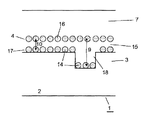
図1に簡易的な光学記憶媒体1の断面図を示す。基板2の上には、ピット構造を有し、例えばアルミ層などの反射金属層を備える読取専用データ層3が配置される。読取専用データ層3の上には、例えばプラスチック材料から形成される第1の誘電体層5が配置される。誘電体層5の上には、超解像近接場効果(Super-RENS)を与えるナノ粒子を備えるマスク層4が配置される。
FIG. 1 shows a cross-sectional view of a simple optical storage medium 1. A read-
誘電体層5は、平坦な面を持つようにして配置され、誘電体層5の上にはナノ粒子が置かれて、そしてそれゆえにマスク層4のナノ粒子とデータ層3との間の距離がピット構造に依存して厚みが変化するようにして決められる。マスク層4の上には、例えばZnS−SiO2材料を備える第2の誘電体層6が配置される。追加の層として、誘電体層6の上にカバー層7が保護層として配置される。データ層3のデータを読み取ることに関し、光学記憶媒体1の上部からレーザービームが当てられて、まずカバー層7に入る。
The
光学記憶媒体1は、特に光学ディスクである。読取専用データ層3は、正のマークまたは負のマークを有するプレス済みのピット構造をとることができて、これは通常のROMディスク、例えばDVDやCDなどで知られているものである。
The optical storage medium 1 is in particular an optical disk. The read-
図2において、例えば30ナノメートル以上(例えば、約40ナノメートル)のピット8のように配置されるマークをもつピット構造を有するデータ層3を備える第1の実施形態が示される。データ層3のピット8は、例えばスタンパー(stamper)により製造することができる。ナノ粒子をもつマスク層4は、ドットで示され、均一な面に配置される様子が示されている。マスク層4は、例えば1〜30ナノメートルの範囲内の厚みを有し、誘電体層5は、20〜50ナノメートルの範囲内の厚みを有する。
In FIG. 2, a first embodiment is shown comprising a
マスク層4のこのように均一な面を得るために、データ層3とマスク層4との間に配置される誘電体層5は、マスク層4のナノ粒子に対して完全に平坦な面を含んでいる。マスク層4のナノ粒子とデータ層3との間の距離は、データ層3にピット8があるときは、それゆえ変化する。マスク層4とピット8の底面との間の距離9は、特に50ナノメートルよりも大きく、ピットがない場合に、距離10は、特に50ナノメートルより小さい。
In order to obtain such a uniform surface of the
ナノ粒子の特性は、それゆえ誘電体層5の不均一な厚さに従って変化することがあり、ナノ粒子がピットに近づいたときに、ナノ粒子の断面の散乱が増大するようにナノ粒子が優先的に選択される。この場合、ナノ粒子によって散乱された光とピットとの間に強い相互作用があり、そして、ピットによる信号変調が増大することがあり、サブ回折限界ピットを検出することができて、それゆえ超解像近接場効果を与える。
The properties of the nanoparticles can therefore vary according to the non-uniform thickness of the
データ層のピット構造に従って、ナノ粒子は、レーザー光が照射されたときに、非近接場において検出可能な信号をもたらして、局所的な表面プラズモンを生成することが想定される。これは、前に述べた非特許文献1の記事に記載されており、AgOX層のナノ粒子効果に関連するものである。 According to the pit structure of the data layer, it is envisaged that the nanoparticles produce a local surface plasmon when they are irradiated with laser light, resulting in a signal that can be detected in a non-near field. This is described in the article of Non-Patent Document 1 described above and relates to the nanoparticle effect of the AgO x layer.
読取専用データ層3のデータを読み取ることについて、特に、ブルーレイディスクシステムと一致する405ナノメートルの青色レーザーダイオードをもつピックアップを用いることができる。この波長をもつレーザーは、現在、高密度データにできる光学ディスクデータを可能にしている。異なる波長のレーザーダイオードが用いられるとき、誘電体層5の厚みはそれに応じて変化させなければならない。
For reading the data of the read-
図3において、負のピット構造をもつデータ層3を備える本発明の第2の実施形態が示されており、ここで、ピット11は、正のマークまたはバンプとして配置されている。ピット11とマスク層4との間の距離12は、それゆえ小さく、距離13はしたがって大きい。誘電体層5は、マスク層4とデータ層3との間に配置されて、完全な平面を備える。そして、誘電体層5上には、マスク層4のナノ粒子が配置される。
In FIG. 3, a second embodiment of the invention comprising a
本実施形態について、データ層3は、例えば30ナノメートル以上の高さ、例えば40ナノメートルの負のマークを備え、そしてマスク層4とデータ層3との間の距離13は、バンプがない場合には50ナノメートルより大きい。距離12は、例えばマスク層4とデータ層3の場所にあるピット11との間が50ナノメートルよりも小さい。誘電体層5の厚さは、例えば20−50ナノメートルの範囲の最小距離と、例えば50−60ナノメートルより大きな最大距離との間のピット構造にしたがってそれゆえ変化する。
For this embodiment, the
図4に本発明の別の実施形態を示す。別の実施形態では、第1のマスク層4に加えて、データ層3上に直接配置されるナノ粒子14をもつ第2のマスク層17を備える。誘電体層13のナノ粒子14は、したがってピット18の底面上にも配置される。ナノ粒子層17と14との間の誘電体層15は平面を有し、マスク層4のナノ粒子16を均一な面にして配置するようにして配置されている。距離9、10、およびピット18の深さは、図2の実施形態において用いられたものと同等の値にすることができる。第2のマスク層17の厚さは特に一定である。誘電体層15の厚さはまた、前の実施形態と同様に最小距離と最大距離との間のピット構造にそれゆえしたがって変化する。図2から4に示す光学記憶媒体の読み取り専用のデータ層3のデータを読み取るために、ブルーレイディスクシステムと同じ405ナノメートルの青色レーザーダイオードのピックアップを特に用いることができる。この波長のレーザーは、現在、最高のデータ密度の光学データディスクを可能にする。異なる波長のレーザーダイオードを用いるとき、誘電体層5の厚さは、それに応じて変えなければならない。
FIG. 4 shows another embodiment of the present invention. In another embodiment, in addition to the
記憶媒体1、特に光学ディスクを製造するために、最初に、ピット構造を含む基板2が製造される。基板2の上には、例えば、スパッタリングにより、データ層3のような反射金属層が配置される。データ層3上で誘電体層5に完全な平面を与えるために、スピンコート法を有利に用いることができる。スパッタリング法を誘電体層5に用いることはできない。なぜなら、そのとき誘電体層5が一定の厚みを有することとなり、したがってナノ粒子をもつマスク層4に対して平らな面を与えることができないからである。誘電体層5は、例えば、20から50ナノメートルの範囲の値となる厚さをもつ薄いプラスチック層であり、スピンコートにより容易に製造できる。
In order to produce a storage medium 1, in particular an optical disc, first a
次のステップにおいて、例えばスパッタリングにより、マスク層4のナノ粒子が誘電体層5の上に配置される。ナノ粒子をもつマスク層4は、特許文献1に記載されているように例えばリアクティブスパッタリングにより製造することができる。次に、カバー層7が、例えばスピンコート方を用いることにより、ディスク上に配置される。さらに、マスク層4とカバー層7との間に第2の誘電体層6を配置することができる。
In the next step, the nanoparticles of the
本発明の他の実施形態もまた、本発明の趣旨および範囲から逸脱することなく当業者により実施することができる。本発明は特に、ブルーレイディスク形式のピックアップを備えるピックアップユニットを用いる記憶媒体に限定されない。本発明は、したがって、本明細書の後に添付の特許請求の範囲に属する。 Other embodiments of the invention may also be practiced by those skilled in the art without departing from the spirit and scope of the invention. The present invention is not particularly limited to a storage medium using a pickup unit including a Blu-ray disc type pickup. The present invention is therefore within the scope of the claims appended hereto.
Claims (9)
前記基板層の上に配置される、プレスされたピット構造を備える読み取り専用のデータ層と、
ナノ粒子を備えて、レーザービームが照射されたときに表面プラズモンを生成することにより超解像近接場効果をもたらすマスク層と、
前記データ層と前記マスク層との間に配置される誘電体層と、
を備え、
前記誘電体層は、スピンコート法により前記データ層の上に配置され、かつ、前記誘電体層の不均一な厚みを与える平面を備え、
前記不均一な厚みは、前記ピット構造に従って変化する
ことを特徴とする光学記憶媒体。A substrate layer;
A read-only data layer comprising a pressed pit structure disposed on the substrate layer;
A mask layer comprising nanoparticles and providing a super-resolution near-field effect by generating surface plasmons when irradiated with a laser beam;
A dielectric layer disposed between the data layer and the mask layer;
With
The dielectric layer is disposed on the data layer by a spin coating method, and includes a plane that gives a non-uniform thickness of the dielectric layer,
The optical storage medium , wherein the non-uniform thickness varies according to the pit structure .
30ナノメートルよりも大きなピット深さをもつ正のピットと、
前記データ層の位置にピットがある場合、前記マスク層と前記データ層との間が50ナノメートルよりも大きい距離と、
前記データ層の位置にピットがない場合、前記マスク層と前記データ層との間が50ナノメートルよりも小さい距離と
を備えることを特徴とする請求項1乃至3のうちのいずれか1項に記載の光学記憶媒体。The data layer is
A positive pit with a pit depth greater than 30 nanometers,
If there is a pit at the location of the data layer, a distance greater than 50 nanometers between the mask layer and the data layer;
The distance between the mask layer and the data layer is less than 50 nanometers when there is no pit at the position of the data layer. The optical storage medium described.
30ナノメートルよりも大きなピット高さをもつ負のピットまたはバンプと、
前記データ層の位置にピットがない場合、前記マスク層と前記データ層との間が50ナノメートルよりも大きい距離と、
前記データ層の位置にピットがある場合、前記マスク層と前記データ層との間が50ナノメートルよりも小さい距離と
を備えることを特徴とする請求項1乃至3のうちのいずれか1項に記載の光学記憶媒体。The data layer is
Negative pits or bumps with a pit height greater than 30 nanometers;
If there are no pits at the data layer, a distance greater than 50 nanometers between the mask layer and the data layer;
The distance between the mask layer and the data layer when there is a pit at the position of the data layer includes a distance smaller than 50 nanometers. The optical storage medium described.
Applications Claiming Priority (3)
| Application Number | Priority Date | Filing Date | Title |
|---|---|---|---|
| EP07100977A EP1950759A1 (en) | 2007-01-23 | 2007-01-23 | Optical storage medium with a mask layer providing a super resolution near filed effect and respective manufacturing method |
| EP07100977.3 | 2007-01-23 | ||
| PCT/EP2008/050602 WO2008090104A1 (en) | 2007-01-23 | 2008-01-21 | Optical storage medium with a mask layer providing a super resolution near field effect, and respective manufacturing method |
Publications (3)
| Publication Number | Publication Date |
|---|---|
| JP2010517202A JP2010517202A (en) | 2010-05-20 |
| JP2010517202A5 JP2010517202A5 (en) | 2011-03-10 |
| JP5145359B2 true JP5145359B2 (en) | 2013-02-13 |
Family
ID=38080987
Family Applications (1)
| Application Number | Title | Priority Date | Filing Date |
|---|---|---|---|
| JP2009546723A Expired - Fee Related JP5145359B2 (en) | 2007-01-23 | 2008-01-21 | Optical storage medium having mask layer providing super-resolution near-field effect, and each manufacturing method |
Country Status (9)
| Country | Link |
|---|---|
| US (1) | US8088465B2 (en) |
| EP (2) | EP1950759A1 (en) |
| JP (1) | JP5145359B2 (en) |
| KR (1) | KR101456312B1 (en) |
| CN (1) | CN101583999B (en) |
| AT (1) | ATE502384T1 (en) |
| BR (1) | BRPI0806510A2 (en) |
| DE (1) | DE602008005555D1 (en) |
| WO (1) | WO2008090104A1 (en) |
Families Citing this family (4)
| Publication number | Priority date | Publication date | Assignee | Title |
|---|---|---|---|---|
| WO2010098758A1 (en) * | 2009-02-26 | 2010-09-02 | Hewlett-Packard Development Company, L.P. | Optical data recording medium |
| EP2346040A1 (en) * | 2010-01-08 | 2011-07-20 | Thomson Licensing | Optical storage medium comprising a super-resolution layer and a read-only data layer |
| EP2387036A1 (en) * | 2010-05-10 | 2011-11-16 | Thomson Licensing | Optical disc comprising two nonlinear layers separated by a spacer layer |
| JP6075288B2 (en) * | 2011-08-09 | 2017-02-08 | パナソニックIpマネジメント株式会社 | Information recording medium, information device, and method of manufacturing information recording medium |
Family Cites Families (8)
| Publication number | Priority date | Publication date | Assignee | Title |
|---|---|---|---|---|
| JPH06176402A (en) * | 1992-11-30 | 1994-06-24 | Victor Co Of Japan Ltd | Optical recording medium |
| KR100922870B1 (en) * | 2002-09-28 | 2009-10-20 | 삼성전자주식회사 | High density optical disc |
| JP2004310803A (en) | 2003-04-01 | 2004-11-04 | Samsung Electronics Co Ltd | Super-resolution near-field structure recording medium, reproducing method and reproducing apparatus |
| US20050221228A1 (en) * | 2004-03-30 | 2005-10-06 | General Electric Company | Near field optical storage mask layer, disk, and fabrication method |
| JP2006276453A (en) * | 2005-03-29 | 2006-10-12 | Mitsubishi Chemicals Corp | Information recording medium and optical recording method |
| CN100399441C (en) * | 2005-05-12 | 2008-07-02 | 索尼株式会社 | Optical recording medium and optical recording and reproducing method |
| JP4591379B2 (en) * | 2005-05-12 | 2010-12-01 | ソニー株式会社 | Optical recording medium and optical recording / reproducing method |
| FR2914775B1 (en) * | 2007-04-06 | 2009-05-15 | Commissariat Energie Atomique | SUPER-RESOLUTION OPTICAL RECORDING MEDIUM |
-
2007
- 2007-01-23 EP EP07100977A patent/EP1950759A1/en not_active Withdrawn
-
2008
- 2008-01-21 BR BRPI0806510-1A patent/BRPI0806510A2/en not_active IP Right Cessation
- 2008-01-21 CN CN2008800022215A patent/CN101583999B/en not_active Expired - Fee Related
- 2008-01-21 KR KR1020097015564A patent/KR101456312B1/en not_active Expired - Fee Related
- 2008-01-21 DE DE602008005555T patent/DE602008005555D1/en active Active
- 2008-01-21 EP EP08708006A patent/EP2106609B1/en not_active Not-in-force
- 2008-01-21 JP JP2009546723A patent/JP5145359B2/en not_active Expired - Fee Related
- 2008-01-21 AT AT08708006T patent/ATE502384T1/en not_active IP Right Cessation
- 2008-01-21 US US12/448,955 patent/US8088465B2/en not_active Expired - Fee Related
- 2008-01-21 WO PCT/EP2008/050602 patent/WO2008090104A1/en not_active Ceased
Also Published As
| Publication number | Publication date |
|---|---|
| KR20090105945A (en) | 2009-10-07 |
| BRPI0806510A2 (en) | 2011-09-13 |
| CN101583999B (en) | 2012-10-31 |
| EP2106609B1 (en) | 2011-03-16 |
| EP1950759A1 (en) | 2008-07-30 |
| KR101456312B1 (en) | 2014-11-03 |
| ATE502384T1 (en) | 2011-04-15 |
| US20100062203A1 (en) | 2010-03-11 |
| CN101583999A (en) | 2009-11-18 |
| US8088465B2 (en) | 2012-01-03 |
| EP2106609A1 (en) | 2009-10-07 |
| JP2010517202A (en) | 2010-05-20 |
| DE602008005555D1 (en) | 2011-04-28 |
| WO2008090104A1 (en) | 2008-07-31 |
Similar Documents
| Publication | Publication Date | Title |
|---|---|---|
| EP2074617B1 (en) | Optical storage medium comprising tracks with positive and negative marks, and stampers and production methods for manufacturing of the optical storage medium | |
| JP5145359B2 (en) | Optical storage medium having mask layer providing super-resolution near-field effect, and each manufacturing method | |
| CN101960522B (en) | Optical storage medium comprising a multilevel data layer | |
| CN101960521B (en) | Optical storage medium comprising inverted super-resolution pits and lands | |
| US8259558B2 (en) | Optical storage medium and apparatus for reading of respective data | |
| JP5524514B2 (en) | High data capacity storage medium with protection code, method for obtaining protection code, and each data reader | |
| EP2092521B1 (en) | Optical storage medium and respective apparatus for recording and/or reading data | |
| US8493832B2 (en) | Optical storage medium having different dimension of recorded marks and spaces on different tracks | |
| EP2131358A1 (en) | Recordable optical storage medium comprising a data layer with a super-resolution near-field structure and respective recorder | |
| EP2387036A1 (en) | Optical disc comprising two nonlinear layers separated by a spacer layer |
Legal Events
| Date | Code | Title | Description |
|---|---|---|---|
| A521 | Request for written amendment filed |
Free format text: JAPANESE INTERMEDIATE CODE: A523 Effective date: 20110121 |
|
| A621 | Written request for application examination |
Free format text: JAPANESE INTERMEDIATE CODE: A621 Effective date: 20110121 |
|
| A977 | Report on retrieval |
Free format text: JAPANESE INTERMEDIATE CODE: A971007 Effective date: 20111214 |
|
| A131 | Notification of reasons for refusal |
Free format text: JAPANESE INTERMEDIATE CODE: A131 Effective date: 20120327 |
|
| A601 | Written request for extension of time |
Free format text: JAPANESE INTERMEDIATE CODE: A601 Effective date: 20120621 |
|
| A602 | Written permission of extension of time |
Free format text: JAPANESE INTERMEDIATE CODE: A602 Effective date: 20120628 |
|
| A521 | Request for written amendment filed |
Free format text: JAPANESE INTERMEDIATE CODE: A523 Effective date: 20120927 |
|
| TRDD | Decision of grant or rejection written | ||
| A01 | Written decision to grant a patent or to grant a registration (utility model) |
Free format text: JAPANESE INTERMEDIATE CODE: A01 Effective date: 20121026 |
|
| A01 | Written decision to grant a patent or to grant a registration (utility model) |
Free format text: JAPANESE INTERMEDIATE CODE: A01 |
|
| A61 | First payment of annual fees (during grant procedure) |
Free format text: JAPANESE INTERMEDIATE CODE: A61 Effective date: 20121126 |
|
| FPAY | Renewal fee payment (event date is renewal date of database) |
Free format text: PAYMENT UNTIL: 20151130 Year of fee payment: 3 |
|
| R150 | Certificate of patent or registration of utility model |
Free format text: JAPANESE INTERMEDIATE CODE: R150 |
|
| LAPS | Cancellation because of no payment of annual fees |