JP5138406B2 - Display device and driving method thereof - Google Patents
Display device and driving method thereof Download PDFInfo
- Publication number
- JP5138406B2 JP5138406B2 JP2008031633A JP2008031633A JP5138406B2 JP 5138406 B2 JP5138406 B2 JP 5138406B2 JP 2008031633 A JP2008031633 A JP 2008031633A JP 2008031633 A JP2008031633 A JP 2008031633A JP 5138406 B2 JP5138406 B2 JP 5138406B2
- Authority
- JP
- Japan
- Prior art keywords
- sensing
- data
- unit
- frame
- signal
- Prior art date
- Legal status (The legal status is an assumption and is not a legal conclusion. Google has not performed a legal analysis and makes no representation as to the accuracy of the status listed.)
- Expired - Fee Related
Links
Images


Classifications
-
- G—PHYSICS
- G06—COMPUTING; CALCULATING OR COUNTING
- G06F—ELECTRIC DIGITAL DATA PROCESSING
- G06F3/00—Input arrangements for transferring data to be processed into a form capable of being handled by the computer; Output arrangements for transferring data from processing unit to output unit, e.g. interface arrangements
- G06F3/01—Input arrangements or combined input and output arrangements for interaction between user and computer
- G06F3/03—Arrangements for converting the position or the displacement of a member into a coded form
- G06F3/041—Digitisers, e.g. for touch screens or touch pads, characterised by the transducing means
- G06F3/0412—Digitisers structurally integrated in a display
-
- G—PHYSICS
- G02—OPTICS
- G02F—OPTICAL DEVICES OR ARRANGEMENTS FOR THE CONTROL OF LIGHT BY MODIFICATION OF THE OPTICAL PROPERTIES OF THE MEDIA OF THE ELEMENTS INVOLVED THEREIN; NON-LINEAR OPTICS; FREQUENCY-CHANGING OF LIGHT; OPTICAL LOGIC ELEMENTS; OPTICAL ANALOGUE/DIGITAL CONVERTERS
- G02F1/00—Devices or arrangements for the control of the intensity, colour, phase, polarisation or direction of light arriving from an independent light source, e.g. switching, gating or modulating; Non-linear optics
- G02F1/01—Devices or arrangements for the control of the intensity, colour, phase, polarisation or direction of light arriving from an independent light source, e.g. switching, gating or modulating; Non-linear optics for the control of the intensity, phase, polarisation or colour
- G02F1/13—Devices or arrangements for the control of the intensity, colour, phase, polarisation or direction of light arriving from an independent light source, e.g. switching, gating or modulating; Non-linear optics for the control of the intensity, phase, polarisation or colour based on liquid crystals, e.g. single liquid crystal display cells
- G02F1/133—Constructional arrangements; Operation of liquid crystal cells; Circuit arrangements
- G02F1/1333—Constructional arrangements; Manufacturing methods
- G02F1/13338—Input devices, e.g. touch panels
-
- G—PHYSICS
- G06—COMPUTING; CALCULATING OR COUNTING
- G06F—ELECTRIC DIGITAL DATA PROCESSING
- G06F3/00—Input arrangements for transferring data to be processed into a form capable of being handled by the computer; Output arrangements for transferring data from processing unit to output unit, e.g. interface arrangements
- G06F3/01—Input arrangements or combined input and output arrangements for interaction between user and computer
- G06F3/03—Arrangements for converting the position or the displacement of a member into a coded form
- G06F3/041—Digitisers, e.g. for touch screens or touch pads, characterised by the transducing means
- G06F3/0416—Control or interface arrangements specially adapted for digitisers
- G06F3/04166—Details of scanning methods, e.g. sampling time, grouping of sub areas or time sharing with display driving
-
- G—PHYSICS
- G06—COMPUTING; CALCULATING OR COUNTING
- G06F—ELECTRIC DIGITAL DATA PROCESSING
- G06F3/00—Input arrangements for transferring data to be processed into a form capable of being handled by the computer; Output arrangements for transferring data from processing unit to output unit, e.g. interface arrangements
- G06F3/01—Input arrangements or combined input and output arrangements for interaction between user and computer
- G06F3/03—Arrangements for converting the position or the displacement of a member into a coded form
- G06F3/041—Digitisers, e.g. for touch screens or touch pads, characterised by the transducing means
- G06F3/0416—Control or interface arrangements specially adapted for digitisers
- G06F3/0418—Control or interface arrangements specially adapted for digitisers for error correction or compensation, e.g. based on parallax, calibration or alignment
- G06F3/04186—Touch location disambiguation
-
- G—PHYSICS
- G06—COMPUTING; CALCULATING OR COUNTING
- G06F—ELECTRIC DIGITAL DATA PROCESSING
- G06F3/00—Input arrangements for transferring data to be processed into a form capable of being handled by the computer; Output arrangements for transferring data from processing unit to output unit, e.g. interface arrangements
- G06F3/01—Input arrangements or combined input and output arrangements for interaction between user and computer
- G06F3/03—Arrangements for converting the position or the displacement of a member into a coded form
- G06F3/041—Digitisers, e.g. for touch screens or touch pads, characterised by the transducing means
- G06F3/044—Digitisers, e.g. for touch screens or touch pads, characterised by the transducing means by capacitive means
- G06F3/0447—Position sensing using the local deformation of sensor cells
-
- G—PHYSICS
- G09—EDUCATION; CRYPTOGRAPHY; DISPLAY; ADVERTISING; SEALS
- G09G—ARRANGEMENTS OR CIRCUITS FOR CONTROL OF INDICATING DEVICES USING STATIC MEANS TO PRESENT VARIABLE INFORMATION
- G09G3/00—Control arrangements or circuits, of interest only in connection with visual indicators other than cathode-ray tubes
- G09G3/20—Control arrangements or circuits, of interest only in connection with visual indicators other than cathode-ray tubes for presentation of an assembly of a number of characters, e.g. a page, by composing the assembly by combination of individual elements arranged in a matrix no fixed position being assigned to or needed to be assigned to the individual characters or partial characters
- G09G3/34—Control arrangements or circuits, of interest only in connection with visual indicators other than cathode-ray tubes for presentation of an assembly of a number of characters, e.g. a page, by composing the assembly by combination of individual elements arranged in a matrix no fixed position being assigned to or needed to be assigned to the individual characters or partial characters by control of light from an independent source
- G09G3/36—Control arrangements or circuits, of interest only in connection with visual indicators other than cathode-ray tubes for presentation of an assembly of a number of characters, e.g. a page, by composing the assembly by combination of individual elements arranged in a matrix no fixed position being assigned to or needed to be assigned to the individual characters or partial characters by control of light from an independent source using liquid crystals
- G09G3/3611—Control of matrices with row and column drivers
- G09G3/3648—Control of matrices with row and column drivers using an active matrix
Description
本発明は表示装置及びその駆動方法に関し、特にタッチスクリーンと一体化された表示装置に関する。 The present invention relates to a display device and a driving method thereof, and more particularly to a display device integrated with a touch screen.
パーソナルコンピュータやテレビなどの軽量化及び薄形化が進み、従来のブラウン管(CRT)は今やフラットパネルディスプレイによって駆逐されつつある。フラットパネルディスプレイには、液晶表示装置(LCD)、電界放出表示装置(FED)、有機発光表示装置(OLED)、プラズマディスプレイ(PDP)などがある。 As personal computers and televisions become lighter and thinner, conventional cathode ray tubes (CRTs) are now being driven out by flat panel displays. The flat panel display includes a liquid crystal display (LCD), a field emission display (FED), an organic light emitting display (OLED), a plasma display (PDP), and the like.
フラットパネルディスプレイは一般にアクティブマトリクス型であり、複数の画素が画面にマトリクス状に配列されている。外部から与えられた輝度情報に従って各画素の輝度が個別に制御されることにより、画面に所望の画像が表示される。 A flat panel display is generally an active matrix type, and a plurality of pixels are arranged in a matrix on a screen. A desired image is displayed on the screen by individually controlling the luminance of each pixel according to luminance information given from the outside.
例えば液晶表示装置では2枚の表示パネルが液晶層を間に挟んで貼り合わされている。一方の表示パネルでは複数の画素電極がマトリクス状に配列され、他方の表示パネルでは共通電極が全面を覆っている。各画素電極と共通電極との間の電圧を輝度情報に応じて調節すると、その画素電極と共通電極との間に挟まれた液晶層の部分にはその電圧に応じた強度の電界が生じる。液晶層は誘電率異方性を持つので、液晶層を通過する光の偏光方向が電場の強さに応じて回転する。この偏光方向の変化は偏光子によって各画素の透過率の変化に変換される。従って、各画素電極と共通電極との間の電圧を調節することによってそれらの間に挟まれた液晶層の部分に生じる電界の強さを調節すれば、液晶層のその部分の透過率を調節できる。2枚の表示パネルが外部から光を受けるとき、各画素が調節された透過率に応じた輝度で光る。こうして、輝度情報の示す画像が画面上に再現される。 For example, in a liquid crystal display device, two display panels are bonded together with a liquid crystal layer interposed therebetween. In one display panel, a plurality of pixel electrodes are arranged in a matrix, and in the other display panel, the common electrode covers the entire surface. When the voltage between each pixel electrode and the common electrode is adjusted according to the luminance information, an electric field having an intensity corresponding to the voltage is generated in the portion of the liquid crystal layer sandwiched between the pixel electrode and the common electrode. Since the liquid crystal layer has dielectric anisotropy, the polarization direction of light passing through the liquid crystal layer rotates according to the strength of the electric field. This change in polarization direction is converted into a change in transmittance of each pixel by the polarizer. Therefore, by adjusting the voltage between each pixel electrode and the common electrode to adjust the strength of the electric field generated in the portion of the liquid crystal layer sandwiched between them, the transmittance of that portion of the liquid crystal layer is adjusted. it can. When the two display panels receive light from the outside, each pixel emits light with a luminance corresponding to the adjusted transmittance. Thus, the image indicated by the luminance information is reproduced on the screen.
近年では、携帯電話等の携帯用電子機器や現金自動預払機(ATM)のように、表示装置の画面の上にタッチスクリーンが重ねて設置される場合が増えている。タッチスクリーンとは、利用者の指又はタッチペンなどの外部の物体による画面への接触を検出し、その接触している場所の位置を特定する装置をいう。利用者は指先やタッチペンなどで画面上のタッチスクリーンに触れることにより、コンピュータなどに文字や図形を入力し、画面に表示されたアイコンを操作してコンピュータなどに所望の命令を実行させることができる。 In recent years, touch screens are often placed on the screen of a display device, such as portable electronic devices such as mobile phones and automatic teller machines (ATMs). The touch screen is a device that detects a contact with a screen by an external object such as a user's finger or a touch pen, and identifies the position of the contacted location. By touching the touch screen on the screen with a fingertip or a touch pen, the user can input characters and figures into the computer and operate the icons displayed on the screen to cause the computer to execute desired commands. .
タッチスクリーンを表示装置の画面に重ねて設置する場合、まず、表示装置とタッチスクリーンとをそれぞれ独立な装置として別々の工程で製造し、次に、タッチスクリーンを表示パネルに接着する。しかし、このような表示装置では、製造コストの更なる削減、製品の収率の更なる向上、表示パネルの輝度の更なる向上、製品の更なる薄型化がいずれも困難である。 When the touch screen is placed on the screen of the display device, the display device and the touch screen are first manufactured as separate devices in separate steps, and then the touch screen is bonded to the display panel. However, in such a display device, it is difficult to further reduce the manufacturing cost, further improve the product yield, further improve the brightness of the display panel, and further reduce the thickness of the product.
これらの問題を解決するための手段として、近年、感知素子を表示パネルに内蔵させることにより、表示パネルにタッチスクリーンの機能を併せ持たせる技術の開発が進んでいる。その表示パネルには、複数の画素と共に複数の感知素子が組み込まれ、画面にマトリクス状に配列されている。利用者の指先などが画面に接触するとき、その接触箇所に生じる光学的な変化や応力の変化が感知素子によって検出され、感知信号に変換される。表示装置はその感知信号を解析することにより、利用者の指先などが画面に触れたかどうかを判断し、その接触箇所の位置を特定できる。
感知素子に対しては一般に所定のバイアス電圧が印加される。外部の物体が表示パネルに接触すると、その接触箇所ではバイアス電圧に変化が生じる。その接触箇所に位置する感知素子はそのバイアス電圧の変化を感知信号に変換して出力する。従って、感知素子はバイアス電圧の変化には敏感である。そのため、バイアス電圧が、例えば雷、バックライトのインバータ、電源や駆動回路のスイッチング素子等からのインパルスノイズによって変化した場合にも、感知素子は誤って反応して感知信号を出力する可能性がある。それ故、上記の表示装置には、ノイズに起因する感知信号を画面への物体の接触に起因する感知信号として誤って検出することを防ぐ技術が必要である。 A predetermined bias voltage is generally applied to the sensing element. When an external object touches the display panel, the bias voltage changes at the contact point. The sensing element located at the contact location converts the change in the bias voltage into a sensing signal and outputs it. Thus, the sensing element is sensitive to changes in bias voltage. Therefore, even when the bias voltage changes due to, for example, lightning, backlight inverter, switching noise of power supply or drive circuit, etc., the sensing element may react erroneously and output a sensing signal. . Therefore, the above-described display device needs a technique for preventing erroneous detection of a sensing signal caused by noise as a sensing signal caused by contact of an object with the screen.
本発明の目的は、検出された感知信号からインパルスノイズに起因する成分を除去することにより、タッチスクリーン機能に対する信頼性を更に向上できるタッチスクリーン一体型の表示装置を提供することである。 An object of the present invention is to provide a display device integrated with a touch screen that can further improve the reliability of the touch screen function by removing a component due to impulse noise from a detected sensing signal.
本発明による表示装置は、複数の画素を有する表示パネル、複数の感知部、感知信号処理部、及び、接触判断部を備えている。 The display device according to the present invention includes a display panel having a plurality of pixels, a plurality of sensing units, a sensing signal processing unit, and a contact determination unit.
複数の感知部は、表示パネルにマトリクス状に配列され、外部の物体による表示パネルへの接触に応じて感知信号を生成する。各感知部は好ましくは可変キャパシタを含む。可変キャパシタは好ましくは液晶を誘電体として含み、表示パネルに接触している外部の物体からの圧力に応じて静電容量を変化させる。その静電容量の変化に伴う電気的な変化が感知信号として出力される。複数の感知部は好ましくは行感知部と列感知部とを含む。行感知部はマトリクスの行ごとに連結されている。列感知部はマトリクスの列ごとに連結されている。 The plurality of sensing units are arranged in a matrix on the display panel, and generate sensing signals in response to contact of the external object with the display panel. Each sensing unit preferably includes a variable capacitor. The variable capacitor preferably includes a liquid crystal as a dielectric, and changes the capacitance according to the pressure from an external object in contact with the display panel. An electrical change accompanying the change in the capacitance is output as a sensing signal. The plurality of sensing units preferably include a row sensing unit and a column sensing unit. The row sensing unit is connected for each row of the matrix. The column sensor is connected to each column of the matrix.
感知信号処理部は、所定の周期、好ましくはフレーム周期で複数の感知部から感知信号を読み取り、読み取られた感知信号に基づいて感知データを生成する。感知データは好ましくはデジタルデータである。 The sensing signal processing unit reads sensing signals from a plurality of sensing units at a predetermined period, preferably a frame period, and generates sensing data based on the read sensing signals. The sensed data is preferably digital data.
接触判断部はまず、所定の期間に各感知部から読み取られた感知信号に基づいて生成された感知データを、別の期間に同じ感知部から読み取られた感知信号に基づいて生成された感知データと比較することにより、その所定の期間における各感知部についての第1偏差データを生成する。好ましくは、所定の期間に各感知部から読み取られた感知信号に基づいて生成された感知データと、その所定の期間から所定時間が経過するまでに同じ感知部から読み取られた感知信号に基づいて生成された所定数の感知データのそれぞれとの間の差を求め、その差の最大値を第1偏差データとして設定する。 The contact determination unit first detects the sensing data generated based on the sensing signal read from each sensing unit during a predetermined period, and the sensing data generated based on the sensing signal read from the same sensing unit during another period. Is generated, the first deviation data for each sensing unit in the predetermined period is generated. Preferably, based on sensing data generated based on a sensing signal read from each sensing unit during a predetermined period, and a sensing signal read from the same sensing unit until a predetermined time elapses from the predetermined period. A difference between each of the generated predetermined number of sensing data is obtained, and the maximum value of the difference is set as the first deviation data.
接触判断部は次に、所定の期間における各感知部についての第1偏差データを、同じ期間における異なる感知部についての第1偏差データと比較することにより、その所定の期間における各感知部についての第2偏差データを生成する。好ましくは、比較された第1偏差データの間の差を第2偏差データとして設定する。 The contact determination unit then compares the first deviation data for each sensing unit in a predetermined period with the first deviation data for a different sensing unit in the same period, so that Second deviation data is generated. Preferably, a difference between the compared first deviation data is set as second deviation data.
接触判断部は更に、異なる感知部の間での第2偏差データの変化に基づき、表示パネルに接触している外部の物体の有無を判断し、その接触している場所の位置を特定する。接触判断部は好ましくは、所定数の感知部の間で同じ期間における第2偏差データの最大値を求め、その最大値を基準値と比較する。接触判断部はその比較の結果に基づいて上記の物体の有無を判断し、その接触箇所の位置を特定する。 The contact determination unit further determines the presence / absence of an external object in contact with the display panel based on the change in the second deviation data between the different sensing units, and specifies the position of the contacted location. The contact determination unit preferably obtains the maximum value of the second deviation data in the same period among the predetermined number of sensing units, and compares the maximum value with a reference value. The contact determination unit determines the presence or absence of the object based on the result of the comparison, and specifies the position of the contact location.
感知信号処理部がフレーム周期で感知信号を読み取る場合、接触判断部は好ましくは、まず、各フレームに対する標本フレームグループを、そのフレームとそれに続くフレームとの少なくとも2つから構成する。接触判断部は次に、各フレームとそのフレームに対する標本フレームグループに含まれるフレームとの間で、同じ感知部から読み取られた感知信号に基づいて生成された感知データの差を求める。接触判断部は更に、その差の最大値を第1偏差データとして設定する。 When the sensing signal processing unit reads the sensing signal at a frame period, the touch determination unit preferably first configures a sample frame group for each frame from at least two of the frame and the subsequent frames. Next, the touch determination unit obtains a difference in sensing data generated based on the sensing signal read from the same sensing unit between each frame and a frame included in the sample frame group for the frame. The contact determination unit further sets the maximum value of the difference as the first deviation data.
接触判断部は好ましくは、複数の感知部を2つずつ対にし、各対の感知部の間で同じ期間における第1偏差データの差を求め、その差を第2偏差データとして設定する。接触判断部は更に好ましくは、各感知部について、その感知部から所定距離を隔てている別の感知部を標本感知部とし、各感知部とその標本感知部との間での第1偏差データの差を第2偏差データとして設定する。複数の感知部が行感知部と列感知部とを含む場合、好ましくは、各行感知部に対する標本感知部は他の行の行感知部の中から選択され、各列感知部に対する標本感知部は他の列の列感知部の中から選択される。 Preferably, the contact determination unit pairs a plurality of sensing units, obtains a difference in the first deviation data in the same period between each pair of sensing units, and sets the difference as the second deviation data. More preferably, the contact determination unit uses, as the sample sensing unit, another sensing unit that is separated from the sensing unit by a predetermined distance, and first deviation data between each sensing unit and the sample sensing unit. Is set as the second deviation data. When the plurality of sensing units include a row sensing unit and a column sensing unit, preferably, the sample sensing unit for each row sensing unit is selected from among the row sensing units of other rows, and the sample sensing unit for each column sensing unit is It is selected from the row sensing units of other rows.
接触判断部は好ましくは、所定の期間に同じ感知部から読み取られた感知信号に基づいて生成された複数の感知データの間で平均値を求め、感知データをその平均値に置き換える。感知信号処理部がフレーム周期で感知信号を読み取る場合、接触判断部は好ましくは、まず、同じ標本フレームグループに含まれるフレームごとに同じ感知部から読み取られた感知信号に基づいて生成された感知データの間で平均値を求める。接触判断部は次に、各フレームでの感知データを、そのフレームに対する標本フレームグループについて求められた感知データの平均値に置き換える。 Preferably, the touch determination unit obtains an average value among a plurality of pieces of sensing data generated based on the sensing signal read from the same sensing unit during a predetermined period, and replaces the sensing data with the average value. When the sensing signal processing unit reads the sensing signal in a frame period, the touch determination unit preferably first detects sensing data generated based on the sensing signal read from the same sensing unit for each frame included in the same sample frame group. Find the mean value between. The touch determination unit then replaces the sensing data in each frame with the average value of the sensing data obtained for the sample frame group for that frame.
本発明による表示装置では上記のとおり、接触判断部が、読み取られる期間や読み取り対象の感知部の異なる複数の感知信号に基づいて2種類の偏差データを生成する。第1偏差データは、同じ感知部から読み取られた感知信号に基づいて生成された感知データの時間的な偏差を表す。第2偏差データは、同じ期間に生成された感知データの空間的な偏差を表す。ここで、インパルスノイズに起因する感知信号は一般に、ごく短時間にレベルが変動する信号であり、広い範囲の感知部から一斉に出力される。従って、上記2種類の偏差データはインパルスノイズに起因する感知信号からは影響を受けにくい。それ故、それらの偏差データを利用して画面への物体の接触を判断することにより、インパルスノイズの有無に関わらず、その判断及び接触箇所の位置の特定に対する信頼性を向上できる。 In the display device according to the present invention, as described above, the contact determination unit generates two types of deviation data based on a plurality of sensing signals with different reading periods and sensing units to be read. The first deviation data represents a temporal deviation of the sensing data generated based on the sensing signal read from the same sensing unit. The second deviation data represents a spatial deviation of the sensing data generated during the same period. Here, the sensing signal caused by the impulse noise is generally a signal whose level fluctuates in a very short time, and is output all at once from a wide range of sensing units. Therefore, the two types of deviation data are not easily affected by the sensing signal caused by the impulse noise. Therefore, by determining the contact of the object with the screen using the deviation data, it is possible to improve the reliability of the determination and the determination of the position of the contact location regardless of the presence or absence of the impulse noise.
以下、添付した図面を参照しながら、本発明の好ましい実施形態を詳細に説明する。
図1及び図3は本発明の一実施形態による液晶表示装置のブロック図である。図1は主に、画素のマトリクスを含む表示機能部を示し、図3は主に、感知部のマトリクスを含むタッチスクリーン機能部を示す。図1及び図3に示されているように、この液晶表示装置は好ましくは、液晶表示パネルアセンブリ300、ゲート駆動部400、データ駆動部500、感知信号処理部800、階調電圧生成部550、接触判断部700、及び信号制御部600を有する。
Hereinafter, preferred embodiments of the present invention will be described in detail with reference to the accompanying drawings.
1 and 3 are block diagrams of a liquid crystal display device according to an embodiment of the present invention. FIG. 1 mainly illustrates a display function unit including a matrix of pixels, and FIG. 3 mainly illustrates a touch screen function unit including a matrix of sensing units. As shown in FIGS. 1 and 3, the liquid crystal display device preferably includes a liquid crystal
図1に示されているように、液晶表示パネルアセンブリ300では複数の表示信号線G1〜Gn、D1〜Dmが縦横に延び、それらの間に複数の画素PXがマトリクス状に配列されている。各画素PXは表示信号線G1〜Gn、D1〜Dmによってゲート駆動部400とデータ駆動部500とに接続されている。液晶表示パネルアセンブリ300では更に、図3に示されているように、複数の感知信号線SY1〜SYN、SX1〜SXM、RLが縦横に延び、それらの間に複数の感知部SUがマトリクス状に配列されている。各感知信号線SY1〜SYN、SX1〜SXMの一端にはリセット信号入力部INIが一つずつ接続され、他端には感知信号出力部SOUTが一つずつ接続されている。各感知信号出力部SOUTは出力信号線OY1〜OYN、OX1〜OXMによって感知信号処理部800に接続されている。図1及び図3には示されていないが、画素PXのマトリクスと感知部SUのマトリクスとは好ましくは重ねて配置されている。好ましくは、画素PXのマトリクスには、赤、緑、青の三色の画素PXが交互に配置され、感知部SUはそれら三色の画素PXの組み合わせごとに一つずつ配置されている。その他に、感知部SUが各画素PXに一つずつ配置されていても良い。
As shown in FIG. 1, in the liquid crystal
図2は、液晶表示パネルアセンブリ300に含まれている1つの画素の模式図を示し、図4は、液晶表示パネルアセンブリ300に含まれている1つの感知部の模式図を示す。図2及び図4に示されているように、液晶表示パネルアセンブリ300は好ましくは、薄膜トランジスタ表示パネル100と共通電極表示パネル200とが向かい合わせで貼り合わされている。それら2枚の表示パネル100、200の間には液晶層3が挟まれている。図2及び図4には示されていないが、2枚の表示パネル100、200の間には好ましくは、弾力性を持つスペーサが設置され、2枚の表示パネル100、200の間隔を所定値に保っている。
FIG. 2 is a schematic diagram of one pixel included in the liquid crystal
図1に示されているように、表示信号線は好ましくはn本のゲート線G1〜Gnとm本のデータ線D1〜Dmとを含む。ここで、整数nは好ましくは画素行の総数と等しく、整数mは画素列の総数と等しい。n本のゲート線G1〜Gnは画素マトリクスの中をほぼ行方向に延びている。各ゲート線G1〜Gnは好ましくは一つの画素行にゲート信号を伝達する。データ線D1〜Dmは画素マトリクスの中をほぼ列方向に延びている。各データ線D1〜Dmは好ましくは一つの画素列にデータ電圧を伝達する。図1及び図2には示されていないが、表示信号線はゲート線やデータ線の他にストレージ信号線を含んでいても良い。ストレージ信号線に対しては外部から、好ましくは共通電圧Vcomなどの決められた電圧が印加される。 As shown in FIG. 1, the display signal line preferably includes n gate lines G 1 to G n and m data lines D 1 to D m . Here, the integer n is preferably equal to the total number of pixel rows, and the integer m is equal to the total number of pixel columns. The n gate lines G 1 to G n extend substantially in the row direction in the pixel matrix. Each of the gate lines G 1 to G n preferably transmits a gate signal to one pixel row. The data lines D 1 to D m extend substantially in the column direction in the pixel matrix. Each data line D 1 to D m preferably transmits a data voltage to one pixel column. Although not shown in FIGS. 1 and 2, the display signal line may include a storage signal line in addition to the gate line and the data line. A predetermined voltage such as a common voltage Vcom is preferably applied to the storage signal line from the outside.
図3に示されているように、感知信号線は好ましくは、N本の行感知信号線SY1〜SYNとM本の列感知信号線SX1〜SXMとを含む。ここで、整数Nは好ましくは感知部SUのマトリクスの行数と等しく、整数Mは好ましくは感知部SUのマトリクスの列数と等しい。行感知信号線SY1〜SYNは感知部SUのマトリクスの中をほぼ行方向に延びている。各行感知信号線SY1〜SYNは好ましくは一行の感知部SUから感知信号を読み取る。列感知信号線SX1〜SXMは感知部SUのマトリクスの中をほぼ列方向に延びている。各列感知信号線SX1〜SXMは好ましくは一列の感知部SUから感知信号を読み取る。感知部SUは好ましくは行感知部と列感知部とを含む。行感知部と列感知部とはそれぞれ、N×Mのマトリクスを構成している。行感知部SUは行ごとに異なる行感知信号線SY1〜SYNに接続され、列感知部SUは列ごとに異なる列感知信号線SX1〜SXMに接続されている。 As shown in FIG. 3, the sensing signal lines preferably include N row sensing signal lines SY 1 -SY N and M column sensing signal lines SX 1 -SX M. Here, the integer N is preferably equal to the number of rows in the matrix of the sensing units SU, and the integer M is preferably equal to the number of columns in the matrix of the sensing units SU. Row sensing signal lines SY 1 to SY N extends through the matrix of sensing units SU substantially in a row direction. Each row sensing signal lines SY 1 to SY N preferably reads the sensing signal from the sensing unit SU of one line. The column sensing signal lines SX 1 to SX M extend substantially in the column direction in the matrix of the sensing units SU. Each column sensing signal line SX 1 to SX M preferably reads a sensing signal from one row of sensing units SU. The sensing unit SU preferably includes a row sensing unit and a column sensing unit. Each of the row sensing unit and the column sensing unit constitutes an N × M matrix. It is connected to the row sensor unit SU row each on a separate line sensing signal lines SY 1 to SY N, the column sensor unit SU are connected to different column sensing signal lines SX 1 ~SX M for each column.
図3には示されていないが図4には示されているように、感知信号線は更に複数の基準電圧線RLを含んでいても良い。基準電圧線RLには、好ましくは各行感知信号線SY1〜SYNに沿って行方向に延びているものがN本あり、各列感知信号線SX1〜SXMに沿って列方向に延びているものがM本ある。行方向に延びている各基準電圧線RLは、各行感知信号線SY1〜SYNに連結されている一行の感知部SUに基準電圧を伝達する。列方向に延びている各基準電圧線RLは、各列感知信号線SX1〜SXMに連結されている一列の感知部SUに基準電圧を伝達する。基準電圧は好ましくは、高レベルと低レベルとの間を一定の周期で変動する。尚、基準電圧線RLは省略されても良い。 Although not shown in FIG. 3, as shown in FIG. 4, the sensing signal line may further include a plurality of reference voltage lines RL. The reference voltage lines RL, preferably in the N present which extends in the row direction along the row sensing signal lines SY 1 to SY N, extending in the column direction along the column sensing signal lines SX 1 ~SX M There are M books. Each reference voltage lines RL extending in the row direction, for transmitting the reference voltage to the sensing unit SU of one line which is connected to each row sensing signal lines SY 1 to SY N. Each reference voltage line RL extending in the column direction transmits the reference voltage to one column of sensing units SU connected to the column sensing signal lines SX 1 to SX M. The reference voltage preferably varies between a high level and a low level with a constant period. Note that the reference voltage line RL may be omitted.
図2に示されているように、各画素PXは好ましくは、スイッチング素子Q、液晶キャパシタClc、及びストレージキャパシタCstを含む。尚、ストレージキャパシタCstは省略されても良い。 As shown in FIG. 2, each pixel PX preferably includes a switching element Q, a liquid crystal capacitor Clc, and a storage capacitor Cst. Note that the storage capacitor Cst may be omitted.
スイッチング素子Qは好ましくは、薄膜トランジスタ表示パネル100に備えられた薄膜トランジスタである。図2に示されている、i番目(i=1、2、…、n)のゲート線Giとj番目(j=1、2、…、m)のデータ線Djとに連結されている画素PXでは、スイッチング素子Qの制御端子はi番目のゲート線Giに接続され、入力端子はj番目のデータ線Djに接続され、出力端子は同じ画素の液晶キャパシタClc及びストレージキャパシタCstに接続されている。薄膜トランジスタQは好ましくは、活性層に非晶質シリコンまたは多結晶シリコンを含む。スイッチング素子Qはゲート線Giから伝達されるゲート信号に応じてオンオフし、液晶キャパシタClc及びストレージキャパシタCstをデータ線Djに接続し、又はデータ線Djから分離する。
The switching element Q is preferably a thin film transistor provided in the thin film
液晶キャパシタClcは、薄膜トランジスタ表示パネル100に形成された画素電極191と、共通電極表示パネル200に形成された共通電極270とを2つの端子とみなし、2つの電極191、270の間に挟まれた液晶層3の部分を誘電体とみなしたキャパシタである。ここで、画素電極191は好ましくは各画素PXに一枚ずつ設置され、同じ画素PXのスイッチング素子Qの出力端子に接続されている。そのスイッチング素子Qがターンオンしたとき、画素電極191はそのスイッチング素子Qを通してデータ線Djからデータ電圧を受ける。共通電極270は好ましくは共通電極表示パネル200の全面を覆い、外部から共通電圧Vcomを受ける。尚、図2とは異なり、共通電極270が薄膜トランジスタ表示パネル100に備えられていても良い。その場合、2つの電極191、270の少なくとも1つが線状または棒状に形成されていても良い。
The liquid crystal capacitor Clc is sandwiched between the two
ストレージキャパシタCstは好ましくは、ストレージ信号線と画素電極191とが絶縁体を隔てて重なっている部分から成る。ストレージキャパシタCstはその他に、画素電極191が絶縁体を隔ててi−1番目のゲート線Gi-1に重なっている部分から形成されていても良い。ストレージキャパシタCstは液晶キャパシタClcの容量を補い、画素電極191の電圧を安定化させる。
The storage capacitor Cst preferably includes a portion where the storage signal line and the
色表示方式には、各画素PXが基本色のいずれか1つを固有に表示する空間分割方式、及び、各画素PXが時間に応じて基本色を交互に表示する時間分割方式がある。基本色の空間的な分布、又は時間的な変化によって所望の色相が表現される。基本色の例としては赤、緑、青の三原色がある。図2は空間分割方式の一例であり、各画素PXの画素電極191に対向する共通電極表示パネル200の領域にカラーフィルタ230が備えられている。カラーフィルタ230の色は基本色のいずれか1つを示す。図2とは異なり、カラーフィルタは薄膜トランジスタ表示パネル100に備えられていても良い。その場合、カラーフィルタ230は画素電極191の上を覆っていても、その下地に形成されていても良い。
The color display method includes a space division method in which each pixel PX inherently displays one of the basic colors and a time division method in which each pixel PX alternately displays the basic color according to time. A desired hue is represented by a spatial distribution of the basic colors or a temporal change. Examples of basic colors include the three primary colors red, green, and blue. FIG. 2 shows an example of a space division method, in which a
図2には示されていないが、好ましくは液晶表示パネルアセンブリ300の外面に偏光子が少なくとも一つ接着されている。偏光子は、液晶表示パネルアセンブリ300を透過する光のうち、特定の偏光成分を透過させる。
Although not shown in FIG. 2, at least one polarizer is preferably bonded to the outer surface of the liquid crystal
図4に示されているように、各感知部SUは可変キャパシタCvと基準キャパシタCpとを含む。可変キャパシタCvは好ましくは、行感知信号線または列感知信号線(以下、単に感知信号線という。)SLと共通電極270との間に接続されている。可変キャパシタCvは更に好ましくは、感知信号線SLと共通電極270とを2つの端子とみなし、それらの間に挟まれている液晶層3の部分を誘電体とみなしたキャパシタである。基準キャパシタCpは感知信号線SLと基準電圧線RLとの間に接続されている。基準キャパシタCpは更に好ましくは、基準電圧線RLと感知信号線SLとが絶縁体を隔てて重なっている部分から成る。
As shown in FIG. 4, each sensing unit SU includes a variable capacitor Cv and a reference capacitor Cp. The variable capacitor Cv is preferably connected between the row sensing signal line or the column sensing signal line (hereinafter simply referred to as sensing signal line) SL and the
図5に、同じ感知信号線SLに接続された感知部SUの等価回路を示す。図5に示されているように、各感知部SUでは可変キャパシタCvと基準キャパシタCpとは直列に接続されている。各直列接続では、可変キャパシタCv側の端子に対して共通電圧Vcomが印加され、基準キャパシタCp側の端子に対して基準電圧Vpが印加されている。液晶表示パネルアセンブリ300の画面に利用者の指等が接触して圧力を加えたとき、その接触箇所ではその圧力によって共通電極270が変形し、感知信号線SLからの距離が変化する。その変化に伴い、可変キャパシタCvの静電容量が変化するので、基準キャパシタCpと可変キャパシタCvとの間で電荷の再配置が生じる。その結果、基準キャパシタCpと可変キャパシタCvとの間の接点で電圧Vnが変わる。画面から利用者の指等が離れて圧力が除去されたとき、その箇所ではスペーサの弾力によって共通電極270が元の形に戻り、感知信号線SLからの距離が元の値に戻る。その変化に伴い、可変キャパシタCvの静電容量が元の値に戻るので、基準キャパシタCpと可変キャパシタCvとの間で電荷の再配置が生じ、基準キャパシタCpと可変キャパシタCvとの間の接点で電圧Vnが元の値に戻る。以上のような接点の電圧Vnの変化が感知信号として感知信号線SLに沿って伝達される。
FIG. 5 shows an equivalent circuit of the sensing unit SU connected to the same sensing signal line SL. As shown in FIG. 5, in each sensing unit SU, the variable capacitor Cv and the reference capacitor Cp are connected in series. In each series connection, the common voltage Vcom is applied to the terminal on the variable capacitor Cv side, and the reference voltage Vp is applied to the terminal on the reference capacitor Cp side. When a user's finger or the like touches the screen of the liquid crystal
図5にはリセット信号入力部INIの等価回路も示されている。図5に示されているように、各リセット信号入力部INIは好ましくはリセットトランジスタQrを含む。リセットトランジスタQrは好ましくは液晶表示パネルアセンブリ300の周縁部に形成された薄膜トランジスタであり、更に好ましくは各画素PXのスイッチング素子Qと共に形成される。リセットトランジスタQrの制御端子は感知信号処理部800に接続され、そこからリセット信号RSTを受ける。リセットトランジスタQrの入力端子に対しては外部からリセット電圧Vrが印加される。リセットトランジスタQrの出力端子は感知信号線SLに接続されている。リセットトランジスタQrはリセット信号RSTに応じてオンオフし、所定の期間にリセット電圧Vrを感知信号線SLに対して印加する。
FIG. 5 also shows an equivalent circuit of the reset signal input unit INI. As shown in FIG. 5, each reset signal input unit INI preferably includes a reset transistor Qr. The reset transistor Qr is preferably a thin film transistor formed at the periphery of the liquid crystal
図5には更に感知信号出力部SOUTの等価回路も示されている。図5に示されているように、各感知信号出力部SOUTは好ましくは出力トランジスタQsを含む。出力トランジスタQsは好ましくは液晶表示パネルアセンブリ300の周縁部に形成された薄膜トランジスタであり、更に好ましくは各画素PXのスイッチング素子Qと共に形成される。出力トランジスタQsの制御端子は感知信号線SLに接続され、そこから感知信号を受ける。出力トランジスタQsの入力端子に対しては外部から入力電圧Vsが印加される。出力トランジスタQsの出力端子は出力信号線OL、すなわち、図3に示されている出力信号線OY1〜OYN、OX1〜OXMのいずれかに接続されている。出力トランジスタQsは好ましくは、感知信号線SLからの感知信号のレベルに応じたレベルの出力信号を生成する。ここで、出力信号は電流信号であっても電圧信号であっても良い。
FIG. 5 also shows an equivalent circuit of the sensing signal output unit SOUT. As shown in FIG. 5, each sensing signal output unit SOUT preferably includes an output transistor Qs. The output transistor Qs is preferably a thin film transistor formed at the peripheral edge of the liquid crystal
各出力信号線OY1〜OYN、OX1〜OXMは好ましくは、接続された感知信号出力部SOUTと同じ側に位置する液晶表示パネルアセンブリ300の周縁部に形成されている。図3に示されているように、出力信号線は好ましくは、N本の行出力信号線OY1〜OYNとM本の列出力信号線OX1〜OXMとを含む。各行出力信号線OY1〜OYNの一端は感知信号出力部SOUTを介して各行感知信号線SY1〜SYNに連結され、各列出力信号線OX1〜OXMの一端は感知信号出力部SOUTを介して各列感知信号線SX1〜SXMに接続されている。各出力信号線OY1〜OYN、OX1〜OXMの他端は感知信号処理部800に接続されている。各出力信号線OY1〜OYN、OX1〜OXMは、感知信号出力部SOUTからの出力信号を感知信号処理部800に伝達する。
The output signal lines OY 1 to OY N and OX 1 to OX M are preferably formed on the peripheral edge of the liquid crystal
図1に示されているように、階調電圧生成部550はデータ駆動部500に連結され、データ駆動部500に複数の階調電圧を供給する。それらの階調電圧は好ましくは、画素PXの透過率の調節可能な値の全てに対応づけられている。階調電圧生成部550はその他に、他の階調電圧の基準とされるべき、限られた種類の階調電圧(以下、基準階調電圧という。)のみを生成しても良い。その場合、他の階調電圧はデータ駆動部500によって基準階調電圧から生成される。複数の階調電圧は好ましくは、共通電圧Vcomに対する極性がプラスのものとマイナスのものとの両方を含む。
As shown in FIG. 1, the
図1に示されているように、ゲート駆動部400は信号制御部600とゲート線G1〜Gnとに接続されている。ゲート駆動部400は信号制御部600からゲート制御信号CONT1を受信し、それに従ってゲート信号をゲート線G1〜Gnに対して順番に印加する。ゲート信号は好ましくは、各画素PXのスイッチング素子Qをターンオンさせるゲートオン電圧Vonと、ターンオフさせるゲートオフ電圧Voffとの組み合わせから成る。
As shown in FIG. 1, the
図1に示されているように、データ駆動部500は、信号制御部600、階調電圧生成部550、及びデータ線D1〜Dmに接続されている。データ駆動部500は、信号制御部600からは映像信号DATとデータ制御信号CONT2とを受信し、階調電圧生成部550からは複数の階調電圧を受ける。データ駆動部500は映像信号DATに応じて階調電圧を選択し、データ電圧としてデータ線D1〜Dmに対して印加する。尚、階調電圧生成部550が基準階調電圧のみを提供する場合、データ駆動部500は基準階調電圧を分圧して所望のデータ電圧を生成する。
As shown in Figure 1, the
図1及び図3に示されているように、感知信号処理部800は信号制御部600と出力信号線OY1〜OYN、OX1〜OXMとに接続されている。感知信号処理部800は信号制御部600から感知制御信号CONT3を受信し、それに従ってリセット信号RSTを生成し、各リセット信号入力部INIのリセットトランジスタQrを所定のタイミングでオンオフさせる。感知信号処理部800は更に、感知制御信号CONT3に従い、各感知信号出力部SOUTの出力信号に基づいて感知データDSNを生成する。
As shown in FIGS. 1 and 3, the sensing
好ましくは図3に示されているように、感知信号処理部800は複数の増幅部810を含む。増幅部810は好ましくは出力信号線OY1〜OYN、OX1〜OXMと同数であり、それらに一つずつ連結されている。図5に各増幅部810の等価回路を示す。図5に示されているように、各増幅部810は好ましくは演算増幅器APを含む。演算増幅器APの反転入力端子−は出力信号線OLに接続されている。演算増幅器APの非反転入力端子+に対しては外部から基準電圧Vaが印加される。各増幅部810は演算増幅器APを用い、好ましくは出力トランジスタQsからの出力電流量に対応するレベルの電圧と基準電圧Vaとの間の差を増幅し、感知信号Voとして出力する。図3には示されていないが、感知信号処理部800は好ましくはアナログ−デジタル変換器を更に含む。感知信号処理部800は、各増幅部810から出力される感知信号Voをアナログ−デジタル変換器を用いてデジタル信号に変換し、感知データDSNとして出力する。
Preferably, as shown in FIG. 3, the sensing
図1及び図3に示されているように、接触判断部700は感知信号処理部800から感知データDSNを受信し、それらに基づいて接触情報INFを生成する。接触情報INFは、液晶表示パネルアセンブリ300の画面に接触する外部の物体の有無、及びその接触している場所の位置に関する情報である。接触判断部700は感知データDSNに対して後述の演算処理を行うことにより、上記の物体の有無を判断し、その接触箇所の位置を特定する。接触判断部700は更に、上記の演算処理によって得られた接触情報INFを外部の装置に送出する。接触判断部700による演算処理の詳細については後述する。
As shown in FIGS. 1 and 3, the
図1に示されているように、信号制御部600は、好ましくは外部のグラフィックコントローラ(図示せず)から入力映像信号R、G、B、及び入力制御信号を受信する。入力映像信号R、G、Bは好ましくは各画素PXの輝度情報を含む。その輝度情報では好ましくは、各画素の輝度が所定数の階調で表されている。入力制御信号は好ましくは、垂直同期信号Vsync、水平同期信号Hsync、メインクロック信号MCLK、及びデータイネーブル信号DEを含む。特に、垂直同期信号Vsyncは、入力映像信号のフレームが切り換えられるタイミングを示し、水平同期信号Hsyncは、各フレーム内で水平走査期間が切り換えられるタイミングを示す。1つの水平走査期間の長さ、すなわち1水平周期は、水平同期信号Hsync及びデータイネーブル信号DEの各周期に等しい。
As shown in FIG. 1, the
信号制御部600は更に、入力映像信号R、G、Bを液晶表示パネルアセンブリ300及びデータ駆動部500の動作条件に合うように適切に処理し、映像信号DATに変換する。映像信号DATは好ましくはデジタル信号であり、特に各画素PXの階調の目標値を示す。
Further, the
信号制御部600はその他に、入力制御信号に基づき、ゲート制御信号CONT1、データ制御信号CONT2、及び感知制御信号CONT3を生成する。ゲート制御信号CONT1はゲート駆動部400に出力され、データ制御信号CONT2と映像信号DATとはデータ駆動部500に出力され、感知制御信号CONT3は感知信号処理部800に出力される。図1には示されていないが、信号制御部600は好ましくは、階調電圧生成部550にも制御信号を与えることにより、その動作を制御する。
In addition, the
ゲート制御信号CONT1は好ましくは走査開始信号とゲートクロック信号とを含む。走査開始信号は、ゲート駆動部400がゲート線G1〜Gnに対するゲートオン電圧Vonの印加を開始すべきタイミングを示す。ゲートクロック信号はゲート駆動部400によってゲートオン電圧Vonの出力周期の制御に利用される。ゲート制御信号CONT1はまた、出力イネーブル信号を更に含んでいても良い。出力イネーブル信号は、ゲート駆動部400がゲートオン電圧Vonを持続すべき期間を示す。
The gate control signal CONT1 preferably includes a scan start signal and a gate clock signal. The scan start signal indicates the timing at which the
データ制御信号CONT2は好ましくは、水平同期開始信号、ロード信号、及びデータクロック信号を含む。水平同期開始信号は、各行の画素PXに対する映像信号DATの伝送開始をデータ駆動部500に通知するのに利用される。ロード信号は、データ駆動部500がデータ線D1〜Dmに対してデータ電圧を印加すべきタイミングを示す。データ制御信号CONT2はまた、反転信号を更に含んでいても良い。データ駆動部500は反転信号に応じ、共通電圧Vcomに対するデータ電圧の極性を反転させる。
The data control signal CONT2 preferably includes a horizontal synchronization start signal, a load signal, and a data clock signal. The horizontal synchronization start signal is used to notify the
感知制御信号CONT3は、感知信号処理部800がリセット信号RSTによって各リセット信号入力部INIのリセットトランジスタQrをオンオフさせるべきタイミングを示す。感知制御信号CONT3は更に、感知信号処理部800が各出力信号線OY1〜OYN、OX1〜OXMを通して各感知信号出力部SOUTの出力信号を読み取るべきタイミングを示す。
The sensing control signal CONT3 indicates the timing at which the sensing
ゲート駆動部400、データ駆動部500、階調電圧生成部550、信号制御部600、接触判断部700、感知信号処理部800のそれぞれは好ましくは、少なくとも1つの集積回路チップに組み込まれている。それらのチップは好ましくは、液晶表示パネルアセンブリ300の上に直接装着され、又は、フレキシブル印刷回路フィルムを用いたTCP(tape carrier package)方式で液晶表示パネルアセンブリ300の上に実装されている。その他に、それらのチップが液晶表示パネルアセンブリ300とは別の印刷回路基板の上に実装されていても良い。更に、それらとは異なり、各駆動部400、500、550、600、700、800が信号線G1〜Gn、D1〜Dm、SY1〜SYN、SX1〜SXM、OY1〜OYN、OX1〜OXM、RL、及び各画素PXのスイッチング素子Qと共に、液晶表示パネルアセンブリ300に集積化されていても良い。また、全ての駆動部400、500、600、800を単一のチップに集積していても良い。その場合、それらの駆動部のいずれか、またはそれらを構成する回路素子のいずれかがその単一のチップに外付されていても良い。
Each of the
以上の構成要素を利用し、上記の液晶表示装置は表示動作を以下のように行う。
まず、信号制御部600は外部のグラフィックコントローラから入力画像信号R、G、B、及び入力制御信号を受信し、それらに基づいて映像信号DAT、ゲート制御信号CONT1、データ制御信号CONT2、及び感知制御信号CONT3を生成する。
Using the above components, the liquid crystal display device performs a display operation as follows.
First, the
データ制御信号CONT2に従い、データ駆動部500は1行の画素PXごとに映像信号DATを受信し、各映像信号DATの示す各画素PXの輝度情報に応じて階調電圧を選択し、データ電圧として目標のデータ線D1〜Dmに対して印加する。
In accordance with the data control signal CONT2, the
ゲート駆動部400はゲート制御信号CONT1に従い、水平走査期間ごとにゲートオン電圧Vonをゲート線G1〜Gnに対して順番に、好ましくは1水平周期ずつ印加する。それにより、各ゲート線G1〜Gnに接続されたスイッチング素子Qが1水平周期ずつターンオンする。その結果、各水平走査期間では、データ線D1〜Dmに対して印加されたデータ電圧が、オン状態のスイッチング素子Qを通して同じ画素PXの画素電極191に対して印加される。
In accordance with the gate control signal CONT1, the
各画素PXでは、画素電極191に対して印加されたデータ電圧と共通電圧Vcomとの間の差によって液晶キャパシタClcが充電され、その両端電圧、すなわち、画素電圧が調節される。その液晶キャパシタClcに含まれる液晶層3の部分では液晶分子の配向が画素電圧の大きさに応じて変化するので、その液晶層3の部分を通過した光の偏光方向が変化する。この偏光方向の変化は偏光子によってその画素PXの透過率の変化として現れる。こうして、その画素PXの輝度は映像信号DATの示す階調に調節される。
In each pixel PX, the liquid crystal capacitor Clc is charged by the difference between the data voltage applied to the
各水平走査期間で上記の過程が繰り返される。それにより、全てのゲート線G1〜Gnに対して順番にゲートオン電圧Vonが印加され、全ての画素PXに対してデータ電圧が印加される。こうして、1フレームの画像が液晶表示パネルアセンブリ300の画面に表示される。
The above process is repeated in each horizontal scanning period. Thereby, the gate-on voltage Von is sequentially applied to all the gate lines G 1 to G n , and the data voltage is applied to all the pixels PX. Thus, an image of one frame is displayed on the screen of the liquid crystal
1フレームの表示が終了すれば、次のフレームの表示が開始される。そのとき、信号制御部600は、データ駆動部500に対して印加される反転信号の状態を制御し、データ駆動部500に、各画素PXに対して印加されるべきデータ電圧の極性を直前のフレームでの極性から反転させる(フレーム反転)。更に、同じフレーム内でもデータ駆動部500が反転信号の特性に応じ、同じデータ線を通じて伝達されるデータ電圧の極性を水平走査期間ごとに反転させ(行反転、ドット反転)、又は、同じ画素行に対して印加されるデータ電圧の極性をデータ線ごとに反転させても良い(列反転、ドット反転)。
When the display of one frame is completed, the display of the next frame is started. At that time, the
上記の液晶表示装置は更に、タッチスクリーンとしての感知動作を以下のように行う。
感知信号処理部800は感知制御信号CONT3に従い、まず、リセット信号RSTを所定時間アクティブにする。それにより、各リセット信号入力部INIではリセットトランジスタQrがターンオンし、リセット電圧Vrを感知信号線SLに対して所定時間印加し、各感知信号線SLの電圧をリセット電圧Vrに初期化する。従って、各感知部SUでは基準キャパシタCpと可変キャパシタCvとの間の接点の電圧Vnがリセット電圧Vrに維持される。可変キャパシタCvは共通電圧Vcomとリセット電圧Vrとの間の差によって充電され、基準キャパシタCpはリセット電圧Vrと基準電圧Vpとの間の差によって充電される。更に、各感知信号出力部SOUTでは出力トランジスタQsが出力信号、好ましくは出力電流の量をリセット電圧Vrに応じた値に維持する。所定時間の経過後、感知信号処理部800はリセット信号RSTを元の状態に戻し、各リセットトランジスタQrをターンオフさせる。それにより、各感知信号線SLがフローティング状態に維持される。
The liquid crystal display device further performs a sensing operation as a touch screen as follows.
The sensing
各リセットトランジスタQrのターンオフから更に所定時間が経過した後、好ましくはそのターンオフから1水平周期以内に、感知信号処理部800は感知制御信号CONT3に応じて増幅部810に各出力信号線OLからの出力電流を入力させる。増幅部810はその出力電流に基づいて感知信号Voを生成する。感知信号処理部800は更に、アナログ−デジタル変換器によって感知信号Voを感知データに変換し、接触判断部700に転送する。
After a predetermined time has passed since the turn-off of each reset transistor Qr, preferably within one horizontal period from the turn-off, the sense
信号制御部600は感知制御信号CONT3を用い、感知信号処理部800によるリセット信号RSTの制御から感知データの出力までの一連の動作を、好ましくはフレームごとに1回ずつ行わせる。更に好ましくは、上記の動作を、フレームとフレームとの間のブランキング期間に含まれるフロントポーチ又はバックポーチに行わせる。フロントポーチ及びバックポーチでは感知信号がゲート信号やデータ電圧の影響をあまり受けないので、他の期間より感知信号の信頼度が高い。尚、感知信号処理部800による一連の動作は、複数のフレームごとに1回ずつ行われても、1フレームに2回以上行われても良い。更に、上記の動作がブランキング期間の他の部分、又はフレーム内に行われても良い。
The
感知信号線SLがフローティング状態に維持されている期間中に液晶表示パネルアセンブリ300の画面のいずれかの場所に利用者の指等が接触すれば、その接触箇所に位置する感知部SUでは共通電極270の変形に伴い、可変キャパシタCvと基準キャパシタCpとの間で電荷の再配置が生じ、可変キャパシタCvと基準キャパシタCpとの間の接点の電圧Vnが変動する。従って、その感知部SUに接続された感知信号出力部SOUTでは出力トランジスタQsの制御端子に対して印加される電圧がリセット電圧Vrから変わる。この電圧の変化によって出力トランジスタQsを流れる電流量が変動する。その出力電流量の変動が出力信号線OLを通して感知信号処理部800の各増幅部810によって増幅され、感知信号Voとして出力される。感知信号処理部800は更に、感知信号Voを感知データDSNに変換して接触判断部700に送出する。
If a user's finger or the like touches any place on the screen of the liquid crystal
感知信号出力部SOUTの入力電圧Vsを適切に調節し、かつ、感知信号処理部800の基準電圧Vaと演算増幅器APの利得とを適切に調節することにより、出力トランジスタQsがリセット電圧Vrを受けているときに感知信号Voのレベルを一定の基準レベルに一致させる。それにより、感知データDSNに含まれる誤差が抑えられるので、画面に接触している外部の物体の有無を接触判断部700によって判別する精度、及びその接触箇所の位置を特定する精度を容易に向上できる。
By appropriately adjusting the input voltage Vs of the sense signal output unit SOUT and appropriately adjusting the reference voltage Va of the sense
接触判断部700は感知データDSNを受信し、それらに対して後述の演算処理を行う。それにより、画面に接触している物体の有無を判断し、その接触箇所の位置を特定する。判断の結果、及び特定された接触箇所の位置に関する情報は接触情報INFとして外部の装置に転送される。外部の装置は接触情報INFに基づいて様々な処理を行う。例えば上記の液晶表示装置がある装置の操作画面として利用されている場合、その装置は接触情報INFに応じ、利用者によって選択されたコマンドやデータを判断する。その装置は更に、そのコマンドやデータに応じた情報やメニュー等を示す入力映像信号R、G、Bを液晶表示装置に転送する。こうして、利用者によって選択された画面やメニューなどが操作画面に表示される。
The
以下、図6A〜図8Bを参照しながら、接触判断部700による感知データDSNの処理の詳細について説明する。
接触判断部700は、好ましくはフレームごとに感知信号処理部800から感知データDSNを受信し、各フレームにおける感知データDSNを、それらの源である行感知部SUの属する行ごとに、又は列感知部SUの属する列ごとに分類して格納する。接触判断部700は更に、それらの行及び列ごとに感知データDSNから接触情報INFを個別に生成する。そのとき、いずれの行及び列についても接触情報INFは同じ方式で生成される。各行の感知データDSNに基づいて得られる接触情報INFは特に、感知部SUのマトリクスの行方向における接触箇所の座標値(以下、行座標値という。)を含み、各列の感知データDSNに基づいて得られる接触情報INFは、感知部SUのマトリクスの列方向における接触箇所の座標値(以下、列座標値という。)を含む。
Hereinafter, the details of the processing of the sensing data DSN by the
The
接触箇所の行座標値は好ましくは以下のようにして得られる。
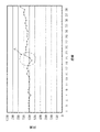
図6Aに、あるフレームで各行の行感知部SUから読み取られた感知データDSNの例を示す。縦軸は各感知データDSNの示す電圧値をmV単位で示す。横軸は、各感知データDSNの源である行感知部SUの属する行の座標を示す。図6Aに示されている例では、特に破線Aで囲まれた部分で感知データDSNが大きく変動していることから、第21行の行感知部SUの位置する場所のいずれかに物体が接触していることが推測される。
The line coordinate value of the contact location is preferably obtained as follows.
FIG. 6A shows an example of the sensing data DSN read from the row sensing unit SU of each row in a certain frame. The vertical axis indicates the voltage value indicated by each sensing data DSN in mV. The horizontal axis represents the coordinates of the row to which the row sensing unit SU that is the source of each sensing data DSN belongs. In the example shown in FIG. 6A, since the sensing data DSN fluctuates greatly particularly in the portion surrounded by the broken line A, the object touches one of the locations where the row sensing unit SU in the 21st row is located. I guess it is.
図6Bに、同じ行の行感知部SUから読み取られた感知データDSNの時間変化、すなわちフレームごとの変化の例を示す。縦軸は各感知データDSNの示す電圧値をmV単位で示す。横軸は各感知データDSNの読み取られたフレームの番号を示す。図6Bに示されている例では、特に破線Bで囲まれた部分で感知データDSNが大きく変動していることから、45〜49番目のフレームで画面に物体が接触し始めたことが推測される。 FIG. 6B shows an example of the time change of the sensing data DSN read from the row sensing unit SU of the same row, that is, a change for each frame. The vertical axis indicates the voltage value indicated by each sensing data DSN in mV. The horizontal axis indicates the number of the frame in which each sensing data DSN is read. In the example shown in FIG. 6B, since the sensing data DSN fluctuates greatly particularly in the portion surrounded by the broken line B, it is estimated that the object starts to touch the screen in the 45th to 49th frames. The
図6Bには、破線Bで囲まれた部分の他にも感知データDSNの変動が見られる。接触判断部700は好ましくは感知データに対して次のフィルタリング処理を行うことにより、感知データの変動のうち、リップルノイズに起因するものを均す。接触判断部700はまず、i番目(i=1、2、3、…)のフレームに対する標本フレームグループを、i番目のフレームとそれに続くi+1番目からi+Nn−1番目までのフレームとの合計Nn枚のフレームから構成する。接触判断部700は次に、i〜i+Nn−1番目の各フレームに同じ第j行(j=1、2、3、…)の行感知部SUから得られた感知データRk,j(k=i、i+1、…、i+Nn−1)の間での平均値Si,jを次式(1)によって計算する。
In FIG. 6B, the variation of the sensing data DSN is seen in addition to the portion surrounded by the broken line B. The

接触判断部700は更に、i番目のフレームにおける第j行の感知データRi,jを、式(1)で得られた平均値Si,jに置き換える。接触判断部700はこのようなフィルタリング処理を、各フレームで得られた全ての行の感知データに対して行い、各行の感知データを平均値に置き換える。尚、標本フレームグループに含まれるフレームの数Nnは好ましくは実験によって決定される。
The
図6Bに示されている感知データに対して上記のフィルタリングを行った結果を図6Cに示す。図6Cに示されているように、上記のフィルタリングにより、感知データの時間変化が緩やかな波形に均されていることが分かる。図6Cでは図6Bと同様に、破線Cで囲まれた部分、すなわち45〜49番目のフレームにおける感知データに大きな変動が認められる。 FIG. 6C shows the result of performing the above filtering on the sensed data shown in FIG. 6B. As shown in FIG. 6C, it can be seen that the time variation of the sensed data is smoothed into a gentle waveform by the above filtering. In FIG. 6C, as in FIG. 6B, a large variation is recognized in the sensing data in the portion surrounded by the broken line C, that is, the 45th to 49th frames.
接触判断部700は更に、上記のフィルタリング処理によって平均値に置き換えられた、i番目(i=1、2、3、…)のフレームにおける第j行(j=1、2、3、…)の感知データSi,jに基づき、i番目のフレームにおける第j行の第1偏差データFi,jを次式(2)によって計算する。
Further, the
Fi,j=Max{Si+k,j−Si,j:k=1、2、…、Nn−1} (2) F i, j = Max {S i + k, j −S i, j : k = 1, 2,..., Nn−1} (2)
すなわち、接触判断部700は、i番目のフレームにおける第j行の感知データSi,jとi+k(k=1、2、…、Nn−1)番目のフレームにおける第j行の感知データSi+k,jとの間の差を演算し、得られたNn−1個の差の中での最大値をi番目のフレームにおける第j行の第1偏差データFi,jとして設定する。接触判断部700は、全ての行の感知データについて同様にして第1偏差データを求める。尚、式(2)では好ましくは、対象とされるフレームの枚数を、上記のフィルタリング処理で利用した標本フレームグループに含まれるフレームの枚数と同じ値Nnに設定する。その他に、式(1)と式(2)とで対象とされるフレームの枚数を別にしても良い。
That is, the
図6Cに示されている、複数のフレームで得られた同じ行の感知データから式(2)を用いて得られる第1偏差データを図6Dに示す。縦軸は各第1偏差データの示す電圧値をmV単位で示す。横軸は各フレームの番号を示す。図6Cに示されている破線Cで囲まれた部分は、図6Dでは破線Dで囲まれた部分、すなわち、49番目のフレームの前後における第1偏差データの大きな変動として顕著に現れる。 FIG. 6D shows the first deviation data obtained using equation (2) from the same row of sensed data obtained in multiple frames shown in FIG. 6C. The vertical axis indicates the voltage value indicated by each first deviation data in mV. The horizontal axis indicates the number of each frame. The part surrounded by the broken line C shown in FIG. 6C appears prominently as a large fluctuation in the first deviation data before and after the 49th frame, that is, the part surrounded by the broken line D in FIG. 6D.
接触判断部700は、全ての行と列との感知データDSNのそれぞれについて同様に第1偏差データを算出する。その結果、図6Dに示されているようなグラフは好ましくは、全ての行及び列について得られる。同じフレームにおける各行の第1偏差データの一例を図7A及び図7Bに示す。縦軸は各第1偏差データの示す電圧値をmV単位で示し、横軸は行座標を示す。図7Aは第1偏差データがインパルスノイズを含んでいない場合を示し、図7Bは第1偏差データがインパルスノイズを含む場合を示す。
The
第1偏差データがインパルスノイズを含んでいない場合は一般に、図7Aに示されている破線Eで囲まれた部分のように、第1偏差データは、限られた行座標の範囲でのみ、所定のしきい値TH1を超える。従って、第1偏差データがそのしきい値TH1を超える行座標の範囲、図7Aでは第20行付近に物体が接触したことが推測される。 In general, when the first deviation data does not include impulse noise, the first deviation data is predetermined only within a limited range of line coordinates, such as a portion surrounded by a broken line E shown in FIG. 7A. Exceeds the threshold TH1. Therefore, it is presumed that the object has touched the range of the line coordinates where the first deviation data exceeds the threshold value TH1, that is, the vicinity of the 20th line in FIG. 7A.
インパルスノイズは一般に、各感知部SUの基準キャパシタCpに対して印加される基準電圧Vp、リセット電圧Vr、入力電圧Vs、または、各増幅部810で利用される基準電圧Vaを一斉に大きく変化させる。更に、第1偏差データは上記の式(1)により、標本フレームグループにおける複数の感知データに基づいて生成される。それらの結果、インパルスノイズが発生したフレームでは一般に、図7Bに示されているように、全ての行座標の第1偏差データがしきい値TH1を大幅に超える。従って、図7Aの場合とは異なり、図7Bに示されている破線Fで囲まれた部分のように、第1偏差データが画面への物体の接触に起因する変動を含んでいても、その接触箇所の位置が特定できないだけでなく、その物体の有無も判断できない。
Impulse noise generally greatly changes the reference voltage Vp applied to the reference capacitor Cp of each sensing unit SU, the reset voltage Vr, the input voltage Vs, or the reference voltage Va used in each
インパルスノイズの影響を弱めるために、接触判断部700は好ましくは、まず、第j行(j=1、2、3、…)からNf行離れた第j+Nf行を、第j行の標本行として設定する。ここで、第j+Nf行に代え、第j−Nf行を第j行の標本行としても良い。接触判断部700は次に、同じi番目(i=1、2、3、…)のフレームにおける第j行の第1偏差データFi,jと、その標本行である第j+Nf行の第1偏差データFi,j+Nfとから、i番目のフレームにおける第j行の第2偏差データFEi,jを次式(3)で計算する。
In order to weaken the influence of impulse noise, the
FEi,j=|Fi,j−Fi,j+Nf| (3) FE i, j = | F i, j −F i, j + Nf | (3)
すなわち、接触判断部700は、各行の第1偏差データとその行の標本行の第1偏差データとの間の差をその行の第2偏差データとして設定する。接触判断部700は全ての行について第2偏差データを同様に生成する。
That is, the
接触判断部700は更に、i番目のフレームにおける全ての行、すなわち第1〜NL行の第2偏差データから、好ましくは次式(4)を満たす第2偏差データFEM、すなわち、i番目のフレームにおける第2偏差データの最大値を求める。ここで、NLは行感知部SUの行の総数を示す。
The
FEM=Max{FEi,j:j=1、2、…、NL−Nf+1} (4) FEM = Max {FE i, j : j = 1, 2,..., N L −Nf + 1} (4)
接触判断部700は続いて、第2偏差データの最大値FEMを所定のしきい値と比較する。第2偏差データの最大値FEMがしきい値より大きい場合、接触判断部700は画面に接触する物体が存在すると判断し、第2偏差データが最大値FEMに等しい行座標を接触箇所の行座標として特定する。
Subsequently, the
同じフレームにおける各行の第2偏差データの一例を図8A及び図8Bに示す。縦軸は各第2偏差データの示す電圧値をmV単位で示し、横軸は行座標を示す。図8Aは、図7Aに示されている、インパルスノイズを含んでいない第1偏差データから得られた第2偏差データを示し、図8Bは、図7Bに示されている、インパルスノイズを含む第1偏差データから得られた第2偏差データを示す。図8A及び図8Bに示されている第2偏差データの計算では、各行とその標本行との間の行数Nfを8に設定している。 An example of the second deviation data of each row in the same frame is shown in FIGS. 8A and 8B. The vertical axis indicates the voltage value indicated by each second deviation data in mV, and the horizontal axis indicates the row coordinate. FIG. 8A shows second deviation data obtained from the first deviation data not including impulse noise shown in FIG. 7A, and FIG. 8B shows the second deviation data including impulse noise shown in FIG. 7B. The 2nd deviation data obtained from 1 deviation data is shown. In the calculation of the second deviation data shown in FIGS. 8A and 8B, the number of rows Nf between each row and its sample row is set to 8.
図7Aに破線Eで示されている、しきい値TH1を超える第1偏差データのピークは、図8Aでは破線Gで囲まれた第2偏差データの2つのピークとして現れる。一方のピークが図7Aに示されているピークの上昇部分に相当し、他方のピークが下降部分に相当する。2つのピークが所定のしきい値TH2を超える場合、接触判断部700は、それら2つのピークが現れる行とそれらの間の行との座標を接触箇所の行座標として特定する。
The peak of the first deviation data exceeding the threshold value TH1 indicated by the broken line E in FIG. 7A appears as two peaks of the second deviation data surrounded by the broken line G in FIG. One peak corresponds to the rising portion of the peak shown in FIG. 7A, and the other peak corresponds to the falling portion. When the two peaks exceed the predetermined threshold value TH2, the
図7Aと図8Aとの間でのピークの関係はインパルスノイズの影響を受けない。実際、図7Bに示されているように、インパルスノイズによって第1偏差データが全ての行で一様に増大してしきい値TH1を超えても、第2偏差データではインパルスノイズによる影響が各行とその標本行との間で相殺されるので、図8Bに示されているように、第2偏差データは一般に、ほとんどの行でしきい値TH2を下回る。一方、図7Bに破線Fで示されている第1偏差データのピークは、図8Bでは破線Hで囲まれた第2偏差データの2つのピークとして現れる。一方のピークが図7Bに示されているピークの上昇部分に相当し、他方のピークが下降部分に相当する。2つのピークはしきい値TH2を超えているので、接触判断部700は、それら2つのピークが現れる行とそれらの間の行との座標を接触箇所の行座標として特定する。
The peak relationship between FIG. 7A and FIG. 8A is not affected by impulse noise. In fact, as shown in FIG. 7B, even if the first deviation data uniformly increases in all rows due to the impulse noise and exceeds the threshold value TH1, the influence of the impulse noise is affected in each row in the second deviation data. As shown in FIG. 8B, the second deviation data is generally below the threshold TH2 for most rows. On the other hand, the peak of the first deviation data indicated by the broken line F in FIG. 7B appears as two peaks of the second deviation data surrounded by the broken line H in FIG. 8B. One peak corresponds to the rising portion of the peak shown in FIG. 7B, and the other peak corresponds to the falling portion. Since the two peaks exceed the threshold value TH2, the
こうして、接触判断部700は第2偏差データを利用することにより、インパルスノイズの有無に関わらず、画面に接触する物体の有無を良好に判断でき、かつその接触箇所の位置を精度良く特定できる。
Thus, by using the second deviation data, the
図9に、接触判断部700の内部構成の一例を示す。図9に示されているように、接触判断部700は好ましくは、受信部710、格納部720、フィルタリング部730、第1データ生成部740、第2データ生成部750、位置判断部760、レジスタ770、及びインターフェース780を含む。
FIG. 9 shows an example of the internal configuration of the
受信部710は、感知信号処理部800から感知部SUの各行及び各列の感知データDSNを、好ましくはフレームごとに受信し、格納部720に出力する。
The receiving
格納部720は好ましくはメモリであり、感知部SUの行及び列ごとにアドレスを割り当て、各アドレスに、複数のフレームにわたる感知データDSNを記憶する。
The
フィルタリング部730は、格納部720に記憶された感知データDSNを式(1)の示す演算によって平均値Sに変換し、格納部720に記憶された感知データDSNをその平均値Sに置き換える。フィルタリング部730はその他に、変換された感知データDSNの平均値Sを、格納部720とは別のメモリに格納しても良い。
The
第1データ生成部740は、フィルタリング部730によって置き換えられた感知データDSNから式(2)の示す演算により、第1偏差データFを生成する。
第2データ生成部750は、第1偏差データFから式(3)の示す演算により、第2偏差データFEを生成する。
The first
The second
位置判断部760は好ましくはプロセッサ、更に好ましくはARMであり、第2偏差データFEから式(4)の示す演算によって第2偏差データの最大値FEMを求める。位置判断部760は更に、得られた最大値FEMをしきい値TH2と比較することにより、画面に接触している物体の有無を判断し、その接触箇所の位置を特定する。位置判断部760は続いて、判断の結果及び特定された位置に関する情報を接触情報INFとして生成する。
The
レジスタ770は、画面に接触している物体の有無を表すフラグ、及び接触情報INFを記憶する。レジスタ770は、位置判断部760に従ってフラグの値を変更し、接触情報INFを更新する。
The
インターフェース780は好ましくはSPI(serial peripheral interface)に準拠のインターフェースである。インターフェース780は、レジスタ770から接触情報INFを読み出し、制御信号などと共に外部の装置に送出する。インターフェース780は更に、外部から、接触判断部700の各構成要素に対するデータや制御信号を受ける。
The
上記の実施形態では、感知部が可変キャパシタ及び基準キャパシタの直列接続を利用する。感知部はその他に、他の方式による感知素子を利用しても良い。例えば、液晶層を挟んで互いに対向する共通電極の部分と感知信号線の部分との少なくとも一方に、他方に向かって突出する部分を設け、感知部として利用しても良い。利用者が画面に接触すると、その接触箇所に位置する感知部では変形した共通電極の部分が対向する感知信号線に接触して短絡が生じる。それにより、感知信号線の電圧が共通電圧に変化する。その電圧変化が感知信号として外部に出力される。その他に、感知部として光センサーを用いても良い。また、2種類以上の感知部を同時に利用しても良い。 In the above embodiment, the sensing unit uses a series connection of a variable capacitor and a reference capacitor. In addition, the sensing unit may use a sensing element of another method. For example, at least one of the common electrode portion and the sensing signal line portion facing each other across the liquid crystal layer may be provided with a portion protruding toward the other to be used as the sensing portion. When the user touches the screen, the deformed common electrode portion contacts the opposing sensing signal line at the sensing portion located at the contact location, causing a short circuit. As a result, the voltage of the sensing signal line changes to the common voltage. The voltage change is output to the outside as a sensing signal. In addition, an optical sensor may be used as the sensing unit. Two or more types of sensing units may be used simultaneously.
上記の実施形態では表示装置が液晶表示装置である。その他に、プラズマディスプレイ、有機発光表示装置等、他の平板表示装置についても本発明は同様に実施可能である。 In the above embodiment, the display device is a liquid crystal display device. In addition, the present invention can be similarly applied to other flat panel display devices such as a plasma display and an organic light emitting display device.
300 液晶表示パネルアセンブリ
400 ゲート駆動部
500 データ駆動部
550 階調電圧生成部
600 信号制御部
700 接触判断部
710 受信部
720 格納部
730 フィルタリング部
740 第1データ生成部
750 第2データ生成部
760 位置判断部
770 レジスタ部
780 インターフェース
800 感知信号処理部
810 増幅部
300 LCD panel assembly
400 Gate drive
500 Data driver
550 gradation voltage generator
600 Signal controller
700 Contact judgment part
710 receiver
720 storage
730 Filtering unit
740 First data generator
750 Second data generator
760 Position determination unit
770 Register section
780 interface
800 Sensing signal processor
810 Amplifier
Claims (10)
前記表示パネルにマトリクス状に配列され、外部の物体による前記表示パネルへの接触に応じて感知信号を生成する複数の感知部、
所定の周期で前記複数の感知部から感知信号を読み取り、読み取られた感知信号に基づいて感知データを生成する感知信号処理部、及び、
所定の期間に各感知部から読み取られた感知信号に基づいて生成された感知データを、別の期間に同じ感知部から読み取られた感知信号に基づいて生成された感知データと比較することにより、その所定の期間における各感知部についての第1偏差データを生成し、所定の期間における各感知部についての第1偏差データを、同じ期間における異なる感知部についての第1偏差データと比較することにより、その所定の期間における各感知部についての第2偏差データを生成し、異なる感知部の間での第2偏差データの変化に基づき、前記表示パネルに接触している外部の物体の有無を判断し、その接触している場所の位置を特定する接触判断部、
を備えている表示装置。 A display panel having a plurality of pixels,
A plurality of sensing units arranged in a matrix on the display panel and generating sensing signals in response to contact of the external object with the display panel;
A sensing signal processing unit that reads sensing signals from the plurality of sensing units at a predetermined period and generates sensing data based on the read sensing signals; and
By comparing the sensing data generated based on the sensing signal read from each sensing unit during a predetermined period with the sensing data generated based on the sensing signal read from the same sensing unit during another period, By generating first deviation data for each sensing unit during the predetermined period and comparing the first deviation data for each sensing unit during the predetermined period with the first deviation data for different sensing units during the same period , Generating second deviation data for each sensor during the predetermined period, and determining whether there is an external object in contact with the display panel based on a change in the second deviation data between the different sensors. And a contact determination unit for identifying the position of the contacted place,
A display device comprising:
前記接触判断部は、各フレームに対する標本フレームグループを、そのフレームとそれに続くフレームとの少なくとも2つから構成し、各フレームとそのフレームに対する標本フレームグループに含まれるフレームとの間で、同じ感知部から読み取られた感知信号に基づいて生成された感知データの差を求め、その差の最大値を第1偏差データとして設定する、
請求項2に記載の表示装置。 The sensing signal processing unit reads sensing signals from the plurality of sensing units in a frame period to generate sensing data,
The touch determination unit includes a sample frame group for each frame including at least two of the frame and a subsequent frame, and the same sensing unit between each frame and a frame included in the sample frame group for the frame. A difference between the sensing data generated based on the sensing signal read from is obtained, and the maximum value of the difference is set as the first deviation data.
The display device according to claim 2.
前記接触判断部は、各フレームに対する標本フレームグループを、そのフレームとそれに続くフレームとの少なくとも2つから構成し、同じ標本フレームグループに含まれるフレームごとに同じ感知部から読み取られた感知信号に基づいて生成された感知データの間で平均値を求め、各フレームでの感知データを、そのフレームに対する標本フレームグループについて求められた感知データの平均値に置き換える、
請求項6に記載の表示装置。 The sensing signal processing unit reads sensing signals from the plurality of sensing units in a frame period to generate sensing data,
The touch determination unit includes a sample frame group for each frame including at least two of the frame and a subsequent frame, and is based on a detection signal read from the same detection unit for each frame included in the same sample frame group. An average value is obtained between the sensed data generated in step (b), and the sensed data in each frame is replaced with the average value of the sensed data obtained for the sample frame group for the frame.
The display device according to claim 6.
各行感知部に対する標本感知部は他の行に並ぶ行感知部の中から選択され、各列感知部に対する標本感知部は他の列に並ぶ列感知部の中から選択される、
請求項5に記載の表示装置。 The plurality of sensing units include a row sensing unit coupled for each row and a column sensing unit coupled for each column,
The sample sensing unit for each row sensing unit is selected from among the row sensing units arranged in other rows, and the sample sensing unit for each column sensing unit is selected from among the column sensing units arranged in other columns.
The display device according to claim 5.
所定の期間に同じ感知部から読み取られた感知信号に基づいて生成された複数の感知データの間で平均値を求め、感知データをその平均値に置き換えるフィルタリング部、
前記フィルタリング部によって置き換えられた感知データの平均値に基づいて第1偏差データを生成する第1データ生成部、
第1偏差データに基づいて第2偏差データを生成する第2データ生成部、
第2偏差データに基づいて前記物体の有無を判断し、その接触している場所の位置を特定する位置判断部、及び、
前記位置判断部の判断結果と特定された位置とに基づき、前記判断結果を示す接触フラグの値と、前記特定された位置を示す接触情報の内容とを変更するレジスタ、
を有する、請求項1に記載の表示装置。 The contact determination unit
A filtering unit that obtains an average value among a plurality of sensing data generated based on sensing signals read from the same sensing unit during a predetermined period, and replaces the sensing data with the average value;
A first data generation unit that generates first deviation data based on an average value of the sensed data replaced by the filtering unit;
A second data generator for generating second deviation data based on the first deviation data;
A position determination unit that determines the presence or absence of the object based on the second deviation data and identifies the position of the contacted place; and
A register that changes the value of the contact flag indicating the determination result and the content of the contact information indicating the specified position based on the determination result of the position determination unit and the specified position;
The display device according to claim 1, comprising:
Applications Claiming Priority (2)
| Application Number | Priority Date | Filing Date | Title |
|---|---|---|---|
| KR1020070014721A KR101350874B1 (en) | 2007-02-13 | 2007-02-13 | Display device and driving method thereof |
| KR10-2007-0014721 | 2007-02-13 |
Publications (3)
| Publication Number | Publication Date |
|---|---|
| JP2008198211A JP2008198211A (en) | 2008-08-28 |
| JP2008198211A5 JP2008198211A5 (en) | 2011-03-17 |
| JP5138406B2 true JP5138406B2 (en) | 2013-02-06 |
Family
ID=39685427
Family Applications (1)
| Application Number | Title | Priority Date | Filing Date |
|---|---|---|---|
| JP2008031633A Expired - Fee Related JP5138406B2 (en) | 2007-02-13 | 2008-02-13 | Display device and driving method thereof |
Country Status (4)
| Country | Link |
|---|---|
| US (1) | US8730198B2 (en) |
| JP (1) | JP5138406B2 (en) |
| KR (1) | KR101350874B1 (en) |
| CN (1) | CN101246270B (en) |
Families Citing this family (35)
| Publication number | Priority date | Publication date | Assignee | Title |
|---|---|---|---|---|
| US7868874B2 (en) * | 2005-11-15 | 2011-01-11 | Synaptics Incorporated | Methods and systems for detecting a position-based attribute of an object using digital codes |
| KR100922852B1 (en) * | 2007-12-11 | 2009-10-20 | 엘지전자 주식회사 | Cleaning device |
| US8564546B1 (en) * | 2008-02-27 | 2013-10-22 | Cypress Semiconductor Corporation | Multiple touch resolve |
| US8902174B1 (en) | 2008-02-29 | 2014-12-02 | Cypress Semiconductor Corporation | Resolving multiple presences over a touch sensor array |
| JP2010139525A (en) * | 2008-12-09 | 2010-06-24 | Sony Corp | Display, display driving method, and electronic apparatus |
| KR101519980B1 (en) | 2008-12-24 | 2015-05-14 | 삼성디스플레이 주식회사 | Method and apparatus for detecting a touch location and touch screen display apparatus having the same |
| TWI426325B (en) * | 2009-04-30 | 2014-02-11 | Innolux Corp | Image display system and method for controlling a touch panel thereof |
| CN101876872B (en) * | 2009-04-30 | 2014-08-13 | 群创光电股份有限公司 | Image display system and control method for touch-control panel |
| JP5519349B2 (en) * | 2009-05-19 | 2014-06-11 | 株式会社ジャパンディスプレイ | Display device and contact detection device |
| KR20120111910A (en) * | 2009-06-29 | 2012-10-11 | 소니 주식회사 | Electrostatic capacitive type touch panel and display device equipped with a touch detection function |
| KR101657215B1 (en) | 2009-09-08 | 2016-09-19 | 삼성디스플레이 주식회사 | Display device including touch panel device and coupling-noise elliminating method |
| US8896548B2 (en) * | 2009-10-09 | 2014-11-25 | Egalax—Empia Technology Inc. | Capacitive touch screen with method and device for converting sensing information including zero cross point |
| JP5424475B2 (en) * | 2009-10-13 | 2014-02-26 | 株式会社ジャパンディスプレイ | Information input device, information input method, information input / output device, information input program, and electronic device |
| CN105045423B (en) | 2010-02-26 | 2020-09-29 | 辛纳普蒂克斯公司 | Modifying demodulation to avoid interference |
| US8963852B2 (en) | 2010-08-20 | 2015-02-24 | Innolux Corporation | Touch panel, driving method for the touch panel, program for getting touch information, and memory media |
| JP5268118B2 (en) * | 2010-08-20 | 2013-08-21 | 群創光電股▲ふん▼有限公司 | Touch panel, touch panel drive method, contact information acquisition program, and recording medium |
| WO2012030183A2 (en) * | 2010-09-01 | 2012-03-08 | Lee Sung Ho | Capacitive touch detection apparatus using level shift, detection method using level shift, and display device having the detection apparatus built therein |
| US8730204B2 (en) | 2010-09-16 | 2014-05-20 | Synaptics Incorporated | Systems and methods for signaling and interference detection in sensor devices |
| KR101165456B1 (en) * | 2011-03-07 | 2012-07-12 | 이성호 | Capacitive type touch detecting means, method and touch screen panel using voltage changing phenomenon, and display device embedding said the capacitive type touch screen panel |
| US8743080B2 (en) | 2011-06-27 | 2014-06-03 | Synaptics Incorporated | System and method for signaling in sensor devices |
| WO2013048195A2 (en) * | 2011-09-29 | 2013-04-04 | Lee Sung Ho | Touch detection means, detection method, and touch screen panel using driving back phenomenon, and display device having touch screen panel embedded therein |
| TW201322070A (en) * | 2011-11-21 | 2013-06-01 | Novatek Microelectronics Corp | Noise filtering method |
| US8766949B2 (en) | 2011-12-22 | 2014-07-01 | Synaptics Incorporated | Systems and methods for determining user input using simultaneous transmission from multiple electrodes |
| CN103187751A (en) * | 2011-12-30 | 2013-07-03 | 致伸科技股份有限公司 | Wireless charging device |
| KR101849585B1 (en) * | 2011-12-30 | 2018-04-18 | 엘지디스플레이 주식회사 | Touch display device and method for driving the same |
| KR101878980B1 (en) * | 2012-03-19 | 2018-08-17 | 엘지디스플레이 주식회사 | Touch sensing apparatus and method for filtering noise thereof |
| JP5787824B2 (en) * | 2012-04-25 | 2015-09-30 | 京セラ株式会社 | Electronics |
| US9063608B2 (en) | 2012-06-14 | 2015-06-23 | Synaptics Incorporated | Systems and methods for sensor devices having a non-commensurate number of transmitter electrodes |
| KR20150086763A (en) * | 2014-01-20 | 2015-07-29 | 삼성디스플레이 주식회사 | Light emitting display device and method for fabricating the same |
| US9176633B2 (en) | 2014-03-31 | 2015-11-03 | Synaptics Incorporated | Sensor device and method for estimating noise in a capacitive sensing device |
| JP6246668B2 (en) * | 2014-06-13 | 2017-12-13 | 株式会社東海理化電機製作所 | Electrostatic detection device |
| KR102253446B1 (en) * | 2014-11-10 | 2021-05-20 | 삼성디스플레이 주식회사 | Display apparatus, method and apparatus for controlling thereof |
| US10025428B2 (en) | 2015-11-19 | 2018-07-17 | Synaptics Incorporated | Method and apparatus for improving capacitive sensing detection |
| US10019122B2 (en) | 2016-03-31 | 2018-07-10 | Synaptics Incorporated | Capacitive sensing using non-integer excitation |
| CN107527588B (en) * | 2017-10-27 | 2020-08-25 | 京东方科技集团股份有限公司 | Display driving circuit, driving method thereof and display device |
Family Cites Families (27)
| Publication number | Priority date | Publication date | Assignee | Title |
|---|---|---|---|---|
| JPS62214426A (en) | 1986-03-17 | 1987-09-21 | Fujitsu Ltd | Panel coordinate position detector |
| JPH056153A (en) | 1991-06-27 | 1993-01-14 | Alps Electric Co Ltd | Liquid crystal display device with touch panel |
| JP3188367B2 (en) | 1994-12-26 | 2001-07-16 | シャープ株式会社 | Coordinate detection device |
| JPH08234910A (en) | 1995-02-22 | 1996-09-13 | Pentel Kk | Touch panel and transparent digitizer in one |
| JPH09282096A (en) | 1996-04-16 | 1997-10-31 | Sharp Corp | Pen input device |
| KR100532094B1 (en) | 1999-01-30 | 2005-11-29 | 삼성전자주식회사 | Noise decreasing apparatus and method of touch panel |
| JP4531272B2 (en) | 2001-01-16 | 2010-08-25 | 株式会社ワコム | Display unit integrated position detection device |
| JP4564680B2 (en) | 2001-03-29 | 2010-10-20 | 株式会社ワコム | Position detection device |
| JP3821002B2 (en) | 2002-02-07 | 2006-09-13 | グンゼ株式会社 | Touch panel device |
| JP2004005415A (en) | 2002-04-19 | 2004-01-08 | Sharp Corp | Input device and input/output integrated display |
| US6998545B2 (en) | 2002-07-19 | 2006-02-14 | E.G.O. North America, Inc. | Touch and proximity sensor control systems and methods with improved signal and noise differentiation |
| US7180508B2 (en) * | 2002-09-17 | 2007-02-20 | Tyco Electronics Corporation | Dynamic corrections for a non-linear touchscreen |
| GB2398916A (en) | 2003-02-28 | 2004-09-01 | Sharp Kk | Display and sensor apparatus |
| KR100510731B1 (en) | 2003-05-31 | 2005-08-30 | 엘지.필립스 엘시디 주식회사 | Method for Driving Touch Panel |
| KR100531800B1 (en) | 2003-12-29 | 2005-12-02 | 엘지전자 주식회사 | Noise filtering method for touch screen |
| KR20050070214A (en) | 2003-12-29 | 2005-07-07 | 엘지전자 주식회사 | Touch response speed control method for touch screen |
| JP2005222266A (en) | 2004-02-05 | 2005-08-18 | Sharp Corp | Display unit with touch sensor and double coated adhesive tape with touch sensor for display unit |
| JP4333428B2 (en) | 2004-03-22 | 2009-09-16 | 株式会社日立製作所 | Proximity position input device |
| KR101133753B1 (en) | 2004-07-26 | 2012-04-09 | 삼성전자주식회사 | Liquid crystal display including sensing element |
| JP4165711B2 (en) | 2004-10-05 | 2008-10-15 | 仁寶電腦工業股▲ふん▼有限公司 | Resistive touchpad signal processing method |
| KR100644650B1 (en) | 2004-11-17 | 2006-11-10 | 삼성전자주식회사 | Apparatus and method for avoiding noise for touch screen panel |
| KR101085447B1 (en) | 2004-12-31 | 2011-11-21 | 삼성전자주식회사 | Touch position detecting device and method of touch position detecting the same and touch screen display device having the same |
| JP3859676B2 (en) | 2005-02-03 | 2006-12-20 | 富士通株式会社 | Touch panel device |
| KR20060108932A (en) | 2005-04-13 | 2006-10-18 | 삼성전자주식회사 | Display device including sensing units and driving method thereof |
| JP4346572B2 (en) | 2005-03-23 | 2009-10-21 | 富士通株式会社 | Control method and apparatus for removing noise in touch panel device, and touch panel device |
| KR101152132B1 (en) | 2005-08-04 | 2012-06-15 | 삼성전자주식회사 | Liquid crystal display including sensing unit |
| US7868874B2 (en) * | 2005-11-15 | 2011-01-11 | Synaptics Incorporated | Methods and systems for detecting a position-based attribute of an object using digital codes |
-
2007
- 2007-02-13 KR KR1020070014721A patent/KR101350874B1/en active IP Right Grant
- 2007-10-31 US US11/931,245 patent/US8730198B2/en active Active
-
2008
- 2008-02-05 CN CN2008100048787A patent/CN101246270B/en not_active Expired - Fee Related
- 2008-02-13 JP JP2008031633A patent/JP5138406B2/en not_active Expired - Fee Related
Also Published As
| Publication number | Publication date |
|---|---|
| US8730198B2 (en) | 2014-05-20 |
| CN101246270B (en) | 2011-06-15 |
| US20080192018A1 (en) | 2008-08-14 |
| KR20080075611A (en) | 2008-08-19 |
| JP2008198211A (en) | 2008-08-28 |
| CN101246270A (en) | 2008-08-20 |
| KR101350874B1 (en) | 2014-01-13 |
Similar Documents
| Publication | Publication Date | Title |
|---|---|---|
| JP5138406B2 (en) | Display device and driving method thereof | |
| JP5485512B2 (en) | Display device and driving method thereof | |
| US10001852B2 (en) | Liquid crystal display device and method of driving the same | |
| JP5281783B2 (en) | Display device and driving method thereof | |
| US10175791B2 (en) | Display device with integrated touch screen | |
| JP6037327B2 (en) | Liquid crystal display | |
| JP5386162B2 (en) | Display device having touch sensing function and driving method thereof | |
| KR20070033532A (en) | Touch sensible display device and driving apparatus therefor and method of processing sensing signals | |
| KR102140791B1 (en) | Touch Controller, Electronic Device and Display Device including Touch Controller, and Method for Touch Sensing | |
| EP1814018A2 (en) | Display device, liquid crystal display, and method thereof | |
| US20160098114A1 (en) | Integrated self-capacitive touch display | |
| US20090122024A1 (en) | Display Device Provided With Optical Input Function | |
| US20110084918A1 (en) | Touch Detection Method and Touch Detection Device and Touch Display Device | |
| US11360626B2 (en) | Display including touch-sensitive circuit and method for operating the same | |
| KR101337259B1 (en) | Display device and driving method thereof | |
| US20110193798A1 (en) | Apparatus for touch sensing, display device, and operating method for the same | |
| TW201426455A (en) | Display device with integrated touch screen and method of driving the same | |
| US20230214061A1 (en) | Display device and method of driving the same | |
| US11500495B2 (en) | Touch display device | |
| CN109491534B (en) | Touch display device | |
| JP4947805B2 (en) | Display device | |
| KR20080054546A (en) | Display device | |
| KR20160150571A (en) | Touch screen controller, touch sensing device, and touch sensing method | |
| KR20070044554A (en) | Display device |
Legal Events
| Date | Code | Title | Description |
|---|---|---|---|
| A521 | Request for written amendment filed |
Free format text: JAPANESE INTERMEDIATE CODE: A523 Effective date: 20110127 |
|
| A621 | Written request for application examination |
Free format text: JAPANESE INTERMEDIATE CODE: A621 Effective date: 20110127 |
|
| A521 | Request for written amendment filed |
Free format text: JAPANESE INTERMEDIATE CODE: A523 Effective date: 20111227 |
|
| A977 | Report on retrieval |
Free format text: JAPANESE INTERMEDIATE CODE: A971007 Effective date: 20120926 |
|
| TRDD | Decision of grant or rejection written | ||
| A01 | Written decision to grant a patent or to grant a registration (utility model) |
Free format text: JAPANESE INTERMEDIATE CODE: A01 Effective date: 20121016 |
|
| A01 | Written decision to grant a patent or to grant a registration (utility model) |
Free format text: JAPANESE INTERMEDIATE CODE: A01 |
|
| A61 | First payment of annual fees (during grant procedure) |
Free format text: JAPANESE INTERMEDIATE CODE: A61 Effective date: 20121114 |
|
| R150 | Certificate of patent or registration of utility model |
Ref document number: 5138406 Country of ref document: JP Free format text: JAPANESE INTERMEDIATE CODE: R150 Free format text: JAPANESE INTERMEDIATE CODE: R150 |
|
| FPAY | Renewal fee payment (event date is renewal date of database) |
Free format text: PAYMENT UNTIL: 20151122 Year of fee payment: 3 |
|
| FPAY | Renewal fee payment (event date is renewal date of database) |
Free format text: PAYMENT UNTIL: 20151122 Year of fee payment: 3 |
|
| S111 | Request for change of ownership or part of ownership |
Free format text: JAPANESE INTERMEDIATE CODE: R313111 |
|
| S631 | Written request for registration of reclamation of domicile |
Free format text: JAPANESE INTERMEDIATE CODE: R313631 |
|
| FPAY | Renewal fee payment (event date is renewal date of database) |
Free format text: PAYMENT UNTIL: 20151122 Year of fee payment: 3 |
|
| R371 | Transfer withdrawn |
Free format text: JAPANESE INTERMEDIATE CODE: R371 |
|
| S631 | Written request for registration of reclamation of domicile |
Free format text: JAPANESE INTERMEDIATE CODE: R313631 |
|
| R350 | Written notification of registration of transfer |
Free format text: JAPANESE INTERMEDIATE CODE: R350 |
|
| S111 | Request for change of ownership or part of ownership |
Free format text: JAPANESE INTERMEDIATE CODE: R313111 |
|
| R350 | Written notification of registration of transfer |
Free format text: JAPANESE INTERMEDIATE CODE: R350 |
|
| R250 | Receipt of annual fees |
Free format text: JAPANESE INTERMEDIATE CODE: R250 |
|
| R250 | Receipt of annual fees |
Free format text: JAPANESE INTERMEDIATE CODE: R250 |
|
| R250 | Receipt of annual fees |
Free format text: JAPANESE INTERMEDIATE CODE: R250 |
|
| R250 | Receipt of annual fees |
Free format text: JAPANESE INTERMEDIATE CODE: R250 |
|
| R250 | Receipt of annual fees |
Free format text: JAPANESE INTERMEDIATE CODE: R250 |
|
| R250 | Receipt of annual fees |
Free format text: JAPANESE INTERMEDIATE CODE: R250 |
|
| LAPS | Cancellation because of no payment of annual fees |