JP5116661B2 - Manufacturing method of multilayer electronic component - Google Patents
Manufacturing method of multilayer electronic component Download PDFInfo
- Publication number
- JP5116661B2 JP5116661B2 JP2008505003A JP2008505003A JP5116661B2 JP 5116661 B2 JP5116661 B2 JP 5116661B2 JP 2008505003 A JP2008505003 A JP 2008505003A JP 2008505003 A JP2008505003 A JP 2008505003A JP 5116661 B2 JP5116661 B2 JP 5116661B2
- Authority
- JP
- Japan
- Prior art keywords
- plating
- ions
- electronic component
- internal electrodes
- laminate
- Prior art date
- Legal status (The legal status is an assumption and is not a legal conclusion. Google has not performed a legal analysis and makes no representation as to the accuracy of the status listed.)
- Active
Links
- 238000004519 manufacturing process Methods 0.000 title claims description 26
- 238000007747 plating Methods 0.000 claims description 166
- 150000002500 ions Chemical class 0.000 claims description 43
- 238000000034 method Methods 0.000 claims description 42
- 239000003638 chemical reducing agent Substances 0.000 claims description 39
- 239000012212 insulator Substances 0.000 claims description 32
- 238000007772 electroless plating Methods 0.000 claims description 31
- 229910021645 metal ion Inorganic materials 0.000 claims description 26
- 230000003197 catalytic effect Effects 0.000 claims description 19
- 229910052759 nickel Inorganic materials 0.000 claims description 18
- 238000005498 polishing Methods 0.000 claims description 16
- 229910052697 platinum Inorganic materials 0.000 claims description 13
- 229910052802 copper Inorganic materials 0.000 claims description 12
- 229910045601 alloy Inorganic materials 0.000 claims description 11
- 239000000956 alloy Substances 0.000 claims description 11
- 229910052709 silver Inorganic materials 0.000 claims description 11
- 229910052737 gold Inorganic materials 0.000 claims description 10
- 239000000919 ceramic Substances 0.000 claims description 9
- NBIIXXVUZAFLBC-UHFFFAOYSA-N phosphoric acid Substances OP(O)(O)=O NBIIXXVUZAFLBC-UHFFFAOYSA-N 0.000 claims description 8
- -1 phosphoric acid compound Chemical class 0.000 claims description 8
- 238000007254 oxidation reaction Methods 0.000 claims description 7
- 229910000147 aluminium phosphate Inorganic materials 0.000 claims description 6
- 230000008021 deposition Effects 0.000 claims description 6
- 238000003756 stirring Methods 0.000 claims description 4
- 239000004327 boric acid Substances 0.000 claims description 2
- 230000001747 exhibiting effect Effects 0.000 claims description 2
- ACVYVLVWPXVTIT-UHFFFAOYSA-M phosphinate Chemical compound [O-][PH2]=O ACVYVLVWPXVTIT-UHFFFAOYSA-M 0.000 claims description 2
- ACVYVLVWPXVTIT-UHFFFAOYSA-N phosphinic acid Chemical compound O[PH2]=O ACVYVLVWPXVTIT-UHFFFAOYSA-N 0.000 claims description 2
- 229910017464 nitrogen compound Inorganic materials 0.000 claims 1
- 150000002830 nitrogen compounds Chemical group 0.000 claims 1
- 230000033116 oxidation-reduction process Effects 0.000 claims 1
- 239000010410 layer Substances 0.000 description 128
- 239000000463 material Substances 0.000 description 15
- 239000003985 ceramic capacitor Substances 0.000 description 14
- 230000007547 defect Effects 0.000 description 12
- 229910052751 metal Inorganic materials 0.000 description 12
- 239000002184 metal Substances 0.000 description 12
- 229910000679 solder Inorganic materials 0.000 description 12
- 239000000758 substrate Substances 0.000 description 9
- 239000003054 catalyst Substances 0.000 description 6
- 238000000151 deposition Methods 0.000 description 6
- 238000009713 electroplating Methods 0.000 description 6
- 238000005488 sandblasting Methods 0.000 description 6
- 230000002950 deficient Effects 0.000 description 5
- IJGRMHOSHXDMSA-UHFFFAOYSA-N nitrogen Substances N#N IJGRMHOSHXDMSA-UHFFFAOYSA-N 0.000 description 5
- 229910052763 palladium Inorganic materials 0.000 description 5
- WSFSSNUMVMOOMR-UHFFFAOYSA-N Formaldehyde Chemical compound O=C WSFSSNUMVMOOMR-UHFFFAOYSA-N 0.000 description 4
- 239000013543 active substance Substances 0.000 description 4
- 238000002474 experimental method Methods 0.000 description 4
- 238000009413 insulation Methods 0.000 description 4
- 239000000126 substance Substances 0.000 description 4
- 239000003990 capacitor Substances 0.000 description 3
- 238000005304 joining Methods 0.000 description 3
- 229910052757 nitrogen Inorganic materials 0.000 description 3
- 238000007517 polishing process Methods 0.000 description 3
- ZOXJGFHDIHLPTG-UHFFFAOYSA-N Boron Chemical compound [B] ZOXJGFHDIHLPTG-UHFFFAOYSA-N 0.000 description 2
- OAKJQQAXSVQMHS-UHFFFAOYSA-N Hydrazine Chemical compound NN OAKJQQAXSVQMHS-UHFFFAOYSA-N 0.000 description 2
- 239000000654 additive Substances 0.000 description 2
- JRPBQTZRNDNNOP-UHFFFAOYSA-N barium titanate Chemical compound [Ba+2].[Ba+2].[O-][Ti]([O-])([O-])[O-] JRPBQTZRNDNNOP-UHFFFAOYSA-N 0.000 description 2
- 229910002113 barium titanate Inorganic materials 0.000 description 2
- 239000010953 base metal Substances 0.000 description 2
- 230000015572 biosynthetic process Effects 0.000 description 2
- 229910052796 boron Inorganic materials 0.000 description 2
- 239000003795 chemical substances by application Substances 0.000 description 2
- 239000003989 dielectric material Substances 0.000 description 2
- 230000000694 effects Effects 0.000 description 2
- 230000003628 erosive effect Effects 0.000 description 2
- 125000002485 formyl group Chemical class [H]C(*)=O 0.000 description 2
- 229910052742 iron Inorganic materials 0.000 description 2
- 239000007769 metal material Substances 0.000 description 2
- 239000000843 powder Substances 0.000 description 2
- VQTSAVIGVPAOQB-UHFFFAOYSA-N [B].[B].[B].[B].[Na] Chemical compound [B].[B].[B].[B].[Na] VQTSAVIGVPAOQB-UHFFFAOYSA-N 0.000 description 1
- 230000000996 additive effect Effects 0.000 description 1
- PNEYBMLMFCGWSK-UHFFFAOYSA-N aluminium oxide Inorganic materials [O-2].[O-2].[O-2].[Al+3].[Al+3] PNEYBMLMFCGWSK-UHFFFAOYSA-N 0.000 description 1
- RJTANRZEWTUVMA-UHFFFAOYSA-N boron;n-methylmethanamine Chemical compound [B].CNC RJTANRZEWTUVMA-UHFFFAOYSA-N 0.000 description 1
- 238000006243 chemical reaction Methods 0.000 description 1
- 239000008139 complexing agent Substances 0.000 description 1
- 150000001875 compounds Chemical class 0.000 description 1
- 238000000280 densification Methods 0.000 description 1
- 238000007599 discharging Methods 0.000 description 1
- 230000005611 electricity Effects 0.000 description 1
- 238000010304 firing Methods 0.000 description 1
- 239000011521 glass Substances 0.000 description 1
- 239000007788 liquid Substances 0.000 description 1
- 230000000873 masking effect Effects 0.000 description 1
- 238000002156 mixing Methods 0.000 description 1
- 238000012986 modification Methods 0.000 description 1
- 230000004048 modification Effects 0.000 description 1
- QJGQUHMNIGDVPM-UHFFFAOYSA-N nitrogen group Chemical group [N] QJGQUHMNIGDVPM-UHFFFAOYSA-N 0.000 description 1
- 229910000510 noble metal Inorganic materials 0.000 description 1
- 239000007800 oxidant agent Substances 0.000 description 1
- 230000001590 oxidative effect Effects 0.000 description 1
- 230000010363 phase shift Effects 0.000 description 1
- 238000001556 precipitation Methods 0.000 description 1
- 230000001603 reducing effect Effects 0.000 description 1
- 239000011347 resin Substances 0.000 description 1
- 229920005989 resin Polymers 0.000 description 1
- 238000007650 screen-printing Methods 0.000 description 1
- 239000004065 semiconductor Substances 0.000 description 1
- 239000002356 single layer Substances 0.000 description 1
- NQXGLOVMOABDLI-UHFFFAOYSA-N sodium oxido(oxo)phosphanium Chemical compound [Na+].[O-][PH+]=O NQXGLOVMOABDLI-UHFFFAOYSA-N 0.000 description 1
- 229920001187 thermosetting polymer Polymers 0.000 description 1
- 229910052718 tin Inorganic materials 0.000 description 1
Images


Classifications
-
- H—ELECTRICITY
- H01—ELECTRIC ELEMENTS
- H01G—CAPACITORS; CAPACITORS, RECTIFIERS, DETECTORS, SWITCHING DEVICES, LIGHT-SENSITIVE OR TEMPERATURE-SENSITIVE DEVICES OF THE ELECTROLYTIC TYPE
- H01G4/00—Fixed capacitors; Processes of their manufacture
- H01G4/002—Details
- H01G4/228—Terminals
- H01G4/232—Terminals electrically connecting two or more layers of a stacked or rolled capacitor
- H01G4/2325—Terminals electrically connecting two or more layers of a stacked or rolled capacitor characterised by the material of the terminals
-
- H—ELECTRICITY
- H01—ELECTRIC ELEMENTS
- H01G—CAPACITORS; CAPACITORS, RECTIFIERS, DETECTORS, SWITCHING DEVICES, LIGHT-SENSITIVE OR TEMPERATURE-SENSITIVE DEVICES OF THE ELECTROLYTIC TYPE
- H01G13/00—Apparatus specially adapted for manufacturing capacitors; Processes specially adapted for manufacturing capacitors not provided for in groups H01G4/00 - H01G11/00
- H01G13/006—Apparatus or processes for applying terminals
-
- H—ELECTRICITY
- H01—ELECTRIC ELEMENTS
- H01G—CAPACITORS; CAPACITORS, RECTIFIERS, DETECTORS, SWITCHING DEVICES, LIGHT-SENSITIVE OR TEMPERATURE-SENSITIVE DEVICES OF THE ELECTROLYTIC TYPE
- H01G4/00—Fixed capacitors; Processes of their manufacture
- H01G4/002—Details
- H01G4/018—Dielectrics
- H01G4/06—Solid dielectrics
- H01G4/08—Inorganic dielectrics
- H01G4/12—Ceramic dielectrics
-
- H—ELECTRICITY
- H01—ELECTRIC ELEMENTS
- H01G—CAPACITORS; CAPACITORS, RECTIFIERS, DETECTORS, SWITCHING DEVICES, LIGHT-SENSITIVE OR TEMPERATURE-SENSITIVE DEVICES OF THE ELECTROLYTIC TYPE
- H01G4/00—Fixed capacitors; Processes of their manufacture
- H01G4/30—Stacked capacitors
Landscapes
- Engineering & Computer Science (AREA)
- Power Engineering (AREA)
- Manufacturing & Machinery (AREA)
- Microelectronics & Electronic Packaging (AREA)
- Chemical & Material Sciences (AREA)
- Ceramic Engineering (AREA)
- Inorganic Chemistry (AREA)
- Ceramic Capacitors (AREA)
- Fixed Capacitors And Capacitor Manufacturing Machines (AREA)
Description
本発明は、積層型電子部品の製造方法に関するものであり、特に、外部電極が積層体の外表面上に、直接、無電解めっきを施すことにより形成される、積層型電子部品の製造方法に関するものである。 The present invention relates to a method for manufacturing a multilayer electronic component, and more particularly, to a method for manufacturing a multilayer electronic component in which an external electrode is formed directly on the outer surface of a multilayer body by electroless plating. Is.
図11に示すように、積層セラミックコンデンサに代表される積層型電子部品101は、一般に、積層された複数の絶縁体層102と、絶縁体層102間の界面に沿って形成された複数の層状の内部電極103および104とを含む、積層体105を備えている。積層体105の一方および他方端面106および107には、それぞれ、複数の内部電極103および複数の内部電極104の各端部が露出していて、これら内部電極103の各端部および内部電極104の各端部を、それぞれ、互いに電気的に接続するように、外部電極108および109が形成されている。
As shown in FIG. 11, a multilayer
外部電極108および109の形成にあたっては、一般に、金属成分とガラス成分とを含む金属ペーストを積層体105の端面106および107上に塗布し、次いで焼き付けることにより、ペースト電極層110がまず形成される。次に、ペースト電極層110上に、たとえばNiを主成分とする第1のめっき層111が形成され、さらにその上に、たとえばSnを主成分とする第2のめっき層112が形成される。すなわち、外部電極108および109の各々は、ペースト電極層110、第1のめっき層111および第2のめっき層112の3層構造より構成される。
In forming
外部電極108および109に対しては、積層型電子部品101が半田を用いて基板に実装される際に、半田との濡れ性が良好であることが求められる。同時に、外部電極108に対しては、互いに電気的に絶縁された状態にある複数の内部電極103を互いに電気的に接続し、かつ、外部電極109に対しては、互いに電気的に絶縁された状態にある複数の内部電極104を互いに電気的に接続する役割が求められる。半田濡れ性の確保の役割は、上述した第2のめっき層112が果たしており、内部電極103および104相互の電気的接続の役割は、ペースト電極層110が果たしている。第1のめっき層111は、はんだ接合時のはんだ食われを防止する役割を果たしている。
The
しかし、ペースト電極層110は、その厚みが数十μm〜数百μmと大きい。したがって、この積層型電子部品101の寸法を一定の規格値に収めるためには、このペースト電極層110の体積を確保する必要が生じる分、不所望にも、静電容量確保のための実効体積を減少させる必要が生じる。一方、めっき層111および112はその厚みが数μm程度であるため、仮に第1のめっき層111および第2のめっき層112のみで外部電極108および109を構成できれば、静電容量確保のための実効体積をより多く確保することができる。
However, the
たとえば、特開2004−146401号公報(特許文献1)には、導電性ペーストを積層体の端面の少なくとも内部電極の積層方向に沿った稜部に、内部電極の引出し部と接触するよう塗布し、この導電性ペーストを焼き付けまたは熱硬化させて導電膜を形成し、さらに、積層体の端面に電解めっきを施し、上記稜部の導電膜と接続されるように電解めっき膜を形成する方法が開示されている。これによると、外部電極の端面における厚みを薄くすることができる。 For example, in Japanese Patent Application Laid-Open No. 2004-146401 (Patent Document 1), a conductive paste is applied to at least a ridge along the stacking direction of the internal electrodes on the end face of the stacked body so as to be in contact with the lead-out portions of the internal electrodes. The conductive paste is baked or thermoset to form a conductive film, and the end surface of the laminate is subjected to electrolytic plating, and the electrolytic plating film is formed so as to be connected to the conductive film on the ridge. It is disclosed. According to this, the thickness at the end face of the external electrode can be reduced.
また、特開昭63−169014号公報(特許文献2)には、積層体の、内部電極が露出した側壁面の全面に対し、側壁面に露出した内部電極が短絡されるように、無電解めっきによって導電性金属膜を析出させる方法が開示されている。 Japanese Patent Laid-Open No. 63-169014 (Patent Document 2) discloses an electroless structure in which the internal electrode exposed on the side wall surface is short-circuited to the entire side wall surface of the laminated body where the internal electrode is exposed. A method for depositing a conductive metal film by plating is disclosed.
しかしながら、前述の特許文献1に記載されている外部電極の形成方法では、露出した内部電極と電解めっき膜とを直接接続することはできるものの、電解めっきを行なう前に、露出した内部電極の引出し部を予め電気的に導通させておくために、導電性ペーストによる導電部を形成する必要がある。この導電性ペーストを特定の箇所に塗布する工程は煩雑である。
However, in the external electrode forming method described in
他方、特許文献2に記載のような無電解めっき法では、形成されためっき膜の緻密性および均質性が低く、積層体の内部にめっき液などが侵入しやすく、信頼性に乏しいという問題があった。これらの問題を改善するには、めっき膜を形成する前にPdなどの触媒活性の高い物質をめっきすべき面に付与しておく方法があり、特許文献2に記載の実施形態では、この方法を用いていた可能性もある。しかし、この触媒付与には、そのための工程が複雑であり、また、めっき膜が所望の場所以外の場所に析出しやすいという問題がある。
On the other hand, in the electroless plating method described in
また、特許文献2に記載の方法では、積層体の内部にある内部電極の材料としてPdやPtを用いているが、これらPdやPtは無電解めっきにおいて還元剤の反応に対して高い触媒活性を示す金属として用いられている。そのため、内部電極に用いる金属材料に関して選択の自由度が低いという問題がある。また、PdやPtは高価な貴金属であるため、積層型電子部品のコストの上昇を招くという問題もある。
Further, in the method described in
さらに、特許文献2に記載の方法では、内部電極の厚さが1μm以上でなければならず、そのため、積層体の大型化を招くとともに、積層型電子部品のコスト高を招くという問題もある。
本発明は、上記のような問題点に鑑みなされたものであって、その目的とするところは、積層型電子部品の外部電極を実質的にめっき析出物のみで形成することにより、実効体積率に優れた積層型電子部品を製造する方法を提供しようとすることである。 The present invention has been made in view of the above-described problems, and its object is to form an effective volume ratio by forming the external electrodes of the multilayer electronic component substantially only by plating deposits. An object of the present invention is to provide a method for manufacturing a laminated electronic component excellent in the above.
本発明の他の目的は、外部電極を形成するにあたって、事前の煩雑な工程、たとえば導電性ペーストの塗布工程や触媒の付与工程などを実施しなくても、緻密なめっき膜からなる外部電極を簡便に形成することができ、かつ高い信頼性をも確保し得る積層型電子部品を製造する方法を提供しようとすることである。 Another object of the present invention is to form an external electrode composed of a dense plating film without performing a complicated process in advance, such as a conductive paste application step or a catalyst application step, in forming the external electrode. An object of the present invention is to provide a method of manufacturing a multilayer electronic component that can be easily formed and can ensure high reliability.
本発明は、積層された複数の絶縁体層と、絶縁体層間の界面に沿って形成された複数の内部電極とを含み、内部電極の各端部が所定の面に露出していて、隣り合う内部電極は上記所定の面において互いに電気的に絶縁されている、積層体を用意する工程と、積層体の所定の面に露出した複数の内部電極の各端部を互いに電気的に接続するように、積層体の所定の面上に外部電極を形成する工程とを含み、内部電極の主成分が、Ni、CuおよびAgから選ばれる少なくとも1種である、積層型電子部品の製造方法に向けられるものであって、上述した技術的課題を解決するため、次のような構成を備えることを特徴としている。 The present invention includes a plurality of laminated insulator layers and a plurality of internal electrodes formed along an interface between the insulator layers, and each end of the internal electrode is exposed on a predetermined surface and adjacent to each other. The matching internal electrodes are electrically insulated from each other on the predetermined surface, and a step of preparing a laminated body is electrically connected to each end of the plurality of internal electrodes exposed on the predetermined surface of the laminated body. as, seen including a step of forming external electrodes on a predetermined surface of the laminated body, the main component of the internal electrodes is at least one selected from Ni, Cu and Ag, the method of manufacturing multilayer electronic components In order to solve the technical problem described above, it is characterized by having the following configuration.
すなわち、外部電極を形成する工程は、積層体を用意する工程において用意された積層体の上記所定の面に露出した複数の内部電極の端部に対し、直接、還元剤およびこの還元剤の酸化還元電位よりも電気化学的に貴な析出電位を有する金属イオンを含有するめっき液を用いて無電解めっきを行なう、無電解めっき工程を備える。 That is, in the step of forming the external electrode, the reducing agent and the oxidizing agent of the reducing agent are directly applied to the ends of the plurality of internal electrodes exposed on the predetermined surface of the laminated body prepared in the step of preparing the laminated body. An electroless plating step of performing electroless plating using a plating solution containing metal ions having a deposition potential electrochemically higher than the reduction potential;
上記無電解めっき工程は、上述の還元剤の酸化反応に対し触媒活性を示す導電性メディアを用意する工程と、上記めっき液中で導電性メディアと積層体とを撹拌する工程と、複数の内部電極の端部に析出しためっき析出物が相互に接続されるようにめっき析出物をめっき成長させる工程とを含む。 The electroless plating step includes a step of preparing a conductive medium exhibiting catalytic activity for the oxidation reaction of the reducing agent, a step of stirring the conductive medium and the laminate in the plating solution, and a plurality of internal components. And a step of growing the plating deposit so that the plating deposits deposited on the end portions of the electrodes are connected to each other.
上述しためっき液中で導電性メディアと積層体とを撹拌する工程は、容器内に収容した導電性メディアと積層体とを、めっき液中で、回転、揺動、傾斜または振動させることによって実施されることが好ましい。 The step of stirring the conductive media and the laminate in the plating solution described above is performed by rotating, swinging, tilting, or vibrating the conductive media and the laminate contained in the container in the plating solution. It is preferred that
本発明において、導電性メディアの直径は、平均値で0.2mm以上であることが好ましい。 In the present invention, the diameter of the conductive media is preferably 0.2 mm or more on average.
還元剤がリン酸系化合物であるとき、めっき液中の金属イオンがNiイオン、CoイオンおよびAuイオンから選ばれる少なくとも1種であり、導電性メディアの少なくとも表面がAu、Ni、CoおよびPtから選ばれる少なくとも1種またはその合金からなることが好ましい。この場合、より好ましくは、リン酸系化合物が次亜リン酸または次亜リン酸塩であり、めっき液中の金属イオンがNiイオンである。 When the reducing agent is a phosphoric acid compound, the metal ions in the plating solution are at least one selected from Ni ions, Co ions, and Au ions, and at least the surface of the conductive media is made of Au, Ni, Co, and Pt. It is preferably made of at least one selected from the alloys or alloys thereof. In this case, more preferably, the phosphoric acid compound is hypophosphorous acid or hypophosphite, and the metal ions in the plating solution are Ni ions.
還元剤がホウ酸系化合物であるとき、めっき液中の金属イオンがNiイオン、Coイオン、PtイオンおよびAuイオンから選ばれる少なくとも1種であり、導電性メディアの少なくとも表面がAu、Ni、CoおよびPtから選ばれる少なくとも1種またはその合金からなることが好ましい。 When the reducing agent is a boric acid compound, the metal ion in the plating solution is at least one selected from Ni ion, Co ion, Pt ion and Au ion, and at least the surface of the conductive medium is Au, Ni, Co And at least one selected from Pt or an alloy thereof.
還元剤が窒素系化合物であるとき、めっき液中の金属イオンがNiイオン、Coイオン、PtイオンおよびAuイオンから選ばれる少なくとも1種であり、導電性メディアの少なくとも表面がCo、NiおよびPtから選ばれる少なくとも1種またはその合金からなることが好ましい。 When the reducing agent is a nitrogen-based compound, the metal ions in the plating solution are at least one selected from Ni ions, Co ions, Pt ions and Au ions, and at least the surface of the conductive medium is made of Co, Ni and Pt. It is preferably made of at least one selected from the alloys or alloys thereof.
還元剤がアルデヒド系化合物であるとき、めっき液中の金属イオンがAgイオン、CuイオンおよびAuイオンから選ばれる少なくとも1種であり、導電性メディアの少なくとも表面がAg、CuおよびAuから選ばれる少なくとも1種またはその合金からなることが好ましい。 When the reducing agent is an aldehyde compound, the metal ion in the plating solution is at least one selected from Ag ions, Cu ions and Au ions, and at least the surface of the conductive medium is at least selected from Ag, Cu and Au. It is preferable that it consists of 1 type or its alloy.
積層体を用意する工程において用意される積層体は、内部電極が露出する所定の面において、絶縁体層の厚み方向に測定した、隣り合う内部電極間の間隔が20μm以下であり、かつ所定の面に対する内部電極の引っ込み長さが1μm以下であることが好ましい。 The laminate prepared in the step of preparing the laminate has a predetermined surface where the internal electrodes are exposed, the distance between adjacent internal electrodes measured in the thickness direction of the insulator layer is 20 μm or less, and It is preferable that the internal electrode is retracted to the surface by 1 μm or less.
あるいは、積層体を用意する工程において用意される積層体は、内部電極が露出する所定の面において、絶縁体層の厚み方向に測定した、隣り合う内部電極間の間隔が50μm以下であり、かつ所定の面に対する内部電極の突出長さが0.1μm以上であることが好ましい。 Alternatively, in the laminate prepared in the step of preparing the laminate, the interval between the adjacent internal electrodes measured in the thickness direction of the insulator layer on the predetermined surface where the internal electrodes are exposed is 50 μm or less, and The protruding length of the internal electrode with respect to the predetermined surface is preferably 0.1 μm or more.
前述したような内部電極の引っ込み長さまたは突出長さの制御は、外部電極を形成する工程の前に、積層体に対し、研磨剤を用いて研磨する工程を実施することによってなされることが好ましい。 Control of the retraction length or the protrusion length of the internal electrode as described above may be performed by performing a step of polishing the laminate with an abrasive before the step of forming the external electrode. preferable.
本発明によれば、積層型電子部品の外部電極を実質的にめっき析出物のみで形成することができるため、実効体積率に優れた積層型電子部品を得ることができる。 According to the present invention, since the external electrode of the multilayer electronic component can be formed substantially only by the plating deposit, a multilayer electronic component having an excellent effective volume ratio can be obtained.
また、本発明によれば、事前の煩雑な工程、たとえば導電性ペーストの塗布工程や触媒の付与工程などを実施しなくても、外部電極の少なくとも内部電極と直接接続される部分を、緻密で均質性の高い無電解めっき析出物によって簡便に形成することができる。その結果、本発明によれば、高い信頼性を確保した積層型電子部品を得ることができる。 In addition, according to the present invention, at least a portion of the external electrode that is directly connected to the internal electrode can be precisely formed without performing a complicated process in advance, such as a conductive paste application process or a catalyst application process. It can be easily formed by electroless plating deposits with high homogeneity. As a result, according to the present invention, it is possible to obtain a multilayer electronic component that ensures high reliability.
さらに、本発明によれば、内部電極の主成分にPd、Ptなどの触媒活性の高い金属を用いなくても、緻密性の高い無電解めっき膜が得られるため、内部電極に安価なNi、Cu、Agといった金属材料を用いることができ、低コストな積層型電子部品を得ることができる。 Furthermore, according to the present invention, a highly dense electroless plating film can be obtained without using a catalytically active metal such as Pd or Pt as a main component of the internal electrode. A metal material such as Cu or Ag can be used, and a low-cost multilayer electronic component can be obtained.
さらに、本発明によれば、内部電極の厚さが1μm未満でも緻密な無電解めっき膜を形成することができるため、小型で低コストな積層型電子部品を得ることができる。 Furthermore, according to the present invention, a dense electroless plating film can be formed even if the thickness of the internal electrode is less than 1 μm, so that a small and low-cost multilayer electronic component can be obtained.
本発明において、導電性メディアの直径の平均値が0.2mm以上であると、めっき膜形成の効率がより良好となる。 In the present invention, when the average value of the diameter of the conductive media is 0.2 mm or more, the efficiency of forming the plating film becomes better.
1,21 積層型電子部品
2 絶縁体層
3,3a,3b,4 内部電極
5,22 積層体
6,7 端面
8,9,24,25 外部電極
10 第1のめっき層
11 第2のめっき層
12a,12b めっき析出物
23 面DESCRIPTION OF
図1ないし図5を参照して、本発明の第1の実施形態による積層型電子部品の製造方法について説明する。 With reference to FIGS. 1-5, the manufacturing method of the multilayer electronic component by the 1st Embodiment of this invention is demonstrated.
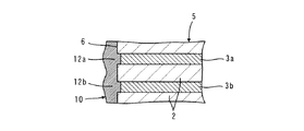
まず、図1に示すように、積層型電子部品1は、積層された複数の絶縁体層2と、絶縁体層2間の界面に沿って形成された複数の層状の内部電極3および4とを含む積層体5を備えている。積層型電子部品1が積層セラミックコンデンサを構成するとき、絶縁体層2は、誘電体セラミックから構成される。積層体5の一方および他方端面6および7には、それぞれ、複数の内部電極3および複数の内部電極4の各端部が露出していて、これら内部電極3の各端部および内部電極4の各端部を、それぞれ、互いに電気的に接続するように、外部電極8および9が形成されている。
First, as shown in FIG. 1, a multilayer
外部電極8および9の各々は、実質的にめっき析出物から構成され、まず、内部電極3および4の露出する端面6および7上に形成される第1のめっき層10と、その上に形成される第2のめっき層11とを備えている。
Each of the
最外層を構成する第2のめっき層11は、半田に対し濡れ性が良好なことが求められるため、SnやAuなどを主成分とすることが望ましい。また、第1のめっき層10は、互いに電気的に絶縁された状態にある各々複数の内部電極3および4を互いに電気的に接続するとともに、はんだ接合時のはんだ食われを防止する役割を果たすことが求められるため、Ni等を主成分とするものが好ましい。
Since the second plating layer 11 constituting the outermost layer is required to have good wettability with respect to solder, it is desirable that Sn, Au, or the like be a main component. In addition, the
内部電極3または4と直接接続される第1のめっき層10は、還元剤を用いて金属イオンを析出させる無電解めっきにより形成されたものであり、通電処理による電解めっきで形成されたものではない。
The
また、第1のめっき層10を無電解めっきにより形成しようとするとき、無電解めっき工程の前に、還元剤の還元作用を促進させる触媒物質、たとえばPd等を、めっき膜を形成すべき面に事前に付与するのが一般的であるが、本発明では、このような触媒物質付与のための工程は設けない。したがって、本発明では、内部電極3および4の露出する端面6および7の各々と第1のめっき層10との間に、触媒物質からなる均一な層は存在しない。当然ながら、内部電極3および4の露出する端面6および7上に直接形成される膜には、導電性ペースト膜、真空蒸着膜、スパッタ膜なども含まれない。
Further, when the
次に、図1に示した積層型電子部品1の製造方法について、外部電極8および9、特に第1のめっき層10の形成方法を中心に、図2ないし図5を参照しながら説明する。
Next, a method for manufacturing the multilayer
図2は、図1に示した積層体5の、内部電極3が露出する一方の端面6付近を拡大して示す図である。図2には、外部電極8を形成する前の状態が示されている。多数存在する内部電極3のうち、図示した領域に位置する2つの内部電極を抽出して、それぞれに参照符号「3a」および「3b」を付している。図2は、内部電極3が露出する端面6の近傍を任意に抽出して示したものであり、内部電極3の特定のものを示すものではない。そして、内部電極3aおよび3bに代表される複数の内部電極3は、この時点では互いに電気的に絶縁された状態にある。
FIG. 2 is an enlarged view showing the vicinity of one
なお、他方の端面7およびそこに露出する内部電極4については、上述した端面6および内部電極3の場合と実質的に同様であるので、図示および説明を省略する。
Since the
第1のめっき層10を形成するにあたり、まず、図2の状態における積層体5を、還元剤、およびこの還元剤の酸化還元電位よりも電気化学的に貴な析出電位を有する金属イオンを含むめっき液で満たされた容器中に投入する。また、この容器中に、還元剤の酸化反応に対し触媒活性を示す導電性メディアを投入する。なお、この導電性メディアは、少なくとも表面が触媒活性を示す物質で構成されていればよく、メディアの内部の材質については特に限定されない。
In forming the
次いで、上記容器を回転、揺動、傾斜または振動させて、積層体5と導電性メディアとをめっき液中で撹拌すると、導電性メディアが、積層体5における内部電極3aおよび3bが露出した端面6に接触するが、その際に、導電性メディアの触媒作用により還元剤が酸化され、その酸化作用による電子が内部電極3aおよび3bに供給されると推定される。
Next, when the
そして、液体中の金属イオンが、その供給された電子を受け取り、内部電極3aおよび3bの露出面に金属として析出する。図3には、上記露出面に析出しためっき析出物12aおよび12bの様子が示されている。この状態における内部電極3aおよび3bは、まだ互いに電気的に絶縁された状態のままである。
Then, the metal ions in the liquid receive the supplied electrons and deposit as metal on the exposed surfaces of the
さらに無電解めっき工程を続けると、それまでに析出しためっき析出物12aおよび12bが核となり、金属イオンの析出がさらに進み、析出しためっき析出物12aおよび12bがさらに成長する。このときの様子を図4に示す。このように析出しためっき析出物12aおよび12bは還元剤に対する触媒作用を有するので、めっき析出物12aおよび12bが大きくなるほど、金属イオンの析出がより促進される。
When the electroless plating process is further continued, the
そして、さらに無電解めっき工程を続けると、金属イオンの析出が進み、各々成長しためっき析出物12aとめっき析出物12bとが互いに接触し、一体化する。この状態が進むと、露出した複数の内部電極3を互いに電気的に接続する第1のめっき層10となる。このときの様子を図5に示す。
When the electroless plating process is further continued, precipitation of metal ions proceeds, and the
以上のように、図2〜図5の経過図に示した現象は、めっき析出物12aおよび12bの成長力の高さに起因するものである。めっき析出物12aおよび12bは、その成長とともに、端面6と平行な方向へ広がりやすく、そして、めっき析出物12aおよび12bが互いに接触したときに一体化しやすくなる。このめっき析出物12aおよび12bの成長力は、めっき浴中の金属イオンの濃度、添加剤、温度などの諸条件を変更することにより調整することが可能である。
As described above, the phenomenon shown in the flow charts of FIGS. 2 to 5 is caused by the high growth power of the
そして、注目すべきは、導電性メディアが還元剤に対して触媒活性を有しているので、事前に触媒付与の工程を経なくても、緻密なめっき層を形成することができるということである。さらに、この導電性メディアは、前述の内部電極3aおよび3bの露出端へ析出しためっき析出物12aおよび12bの密着状態を強固なものにするため、形成された第1のめっき層10の緻密性を向上させるように作用する。
And it should be noted that since the conductive media has catalytic activity with respect to the reducing agent, it is possible to form a dense plating layer without going through the catalyst application step in advance. is there. Further, this conductive medium has a denseness of the formed
なお、導電性メディアの大きさについては、その直径の平均値にして0.2mm以上であることが望ましい。0.2mm以上であると、内部電極3aおよび3bの露出端へのめっき析出物12aおよび12bの析出効率が高くなる。
In addition, about the magnitude | size of an electroconductive medium, it is desirable that the average value of the diameter is 0.2 mm or more. When it is 0.2 mm or more, the deposition efficiency of the
次に、具体的な還元剤の種類に対する、金属イオン種および導電性メディアの材質の関係について説明する。還元剤には、代表的には、リン酸系、ホウ素系、窒素系およびアルデヒド系がある。以下に、これら4種類の還元剤の各々について説明する。 Next, the relationship between the metal ion species and the material of the conductive media with respect to specific reducing agent types will be described. Representative examples of the reducing agent include phosphoric acid, boron, nitrogen, and aldehyde. Below, each of these four types of reducing agents is demonstrated.
リン酸系還元剤としては、たとえば次亜リン酸ナトリウム(NaH2PO2)があり、この酸化反応に触媒活性な物質としては、Au、Ni、CoおよびPtが挙げられ、これらから選ばれる少なくとも1種を導電性メディアの少なくとも表面の材質とすればよい。このときの金属イオンはNiイオン、CoイオンおよびAuイオンのいずれか少なくとも1種にするとよい。Examples of the phosphoric acid-based reducing agent include sodium hypophosphite (NaH 2 PO 2 ), and examples of the catalytically active substance for this oxidation reaction include Au, Ni, Co, and Pt. One type may be a material of at least the surface of the conductive medium. At this time, the metal ions may be at least one of Ni ions, Co ions, and Au ions.
ホウ素系還元剤としては、たとえばテトラホウ素ナトリウム(NaBH4)やジメチルアミンボラン((CH3)2NHBH3)等があり、この酸化反応に触媒活性な物質としては、Au、Ni、CoおよびPtが挙げられ、これらから選ばれる少なくとも1種を導電性メディアの少なくとも表面の材質とすればよい。このときの金属イオンはNiイオン、Coイオン、AuイオンおよびPtイオンのいずれか少なくとも1種にするとよい。Examples of the boron-based reducing agent include sodium tetraboron (NaBH 4 ) and dimethylamine borane ((CH 3 ) 2 NHBH 3 ). Examples of catalytically active substances for this oxidation reaction include Au, Ni, Co, and Pt. And at least one selected from these may be used as the material of at least the surface of the conductive medium. At this time, the metal ions may be at least one of Ni ions, Co ions, Au ions, and Pt ions.
窒素系還元剤としては、たとえばヒドラジン(N2H4)があり、この酸化反応に触媒活性な物質としては、Ni、CoおよびPtが挙げられ、これらから選ばれる少なくとも1種を導電性メディアの少なくとも表面の材質とすればよい。このときの金属イオンはNiイオン、CoイオンおよびPtイオンのいずれか少なくとも1種にするとよい。Examples of the nitrogen-based reducing agent include hydrazine (N 2 H 4 ). Examples of the catalytically active substance for this oxidation reaction include Ni, Co, and Pt. At least one selected from these is used as a conductive medium. At least the surface material may be used. At this time, the metal ions may be at least one of Ni ions, Co ions, and Pt ions.
アルデヒド系還元剤としては、たとえばホルムアルデヒド(HCHO)があり、この酸化反応に触媒活性な物質としては、Ag、CuおよびAuが挙げられ、これらから選ばれる少なくとも1種を導電性メディアの少なくとも表面の材質とすればよい。このときの金属イオンはAgイオン、CuイオンおよびAuイオンのいずれか少なくとも1種にするとよい。 Examples of the aldehyde-based reducing agent include formaldehyde (HCHO). Examples of the catalytically active substance for this oxidation reaction include Ag, Cu, and Au. At least one selected from these is used on at least the surface of the conductive medium. A material may be used. At this time, the metal ions may be at least one of Ag ions, Cu ions, and Au ions.
以上、4つの具体的な組合せの例を示したが、本発明は上記の4つの組合せに限られるわけではなく、析出させたい金属種に適合する還元剤を選定し、その還元剤に適合する触媒物質を導電性メディアに採用すればよく、その種類は問われるものではない。また、錯化剤や添加剤の種類・濃度、pH、温度、混合条件などの各種めっき条件は、上記還元剤や金属イオンの種類によって、適宜調整される。 In the above, examples of four specific combinations have been shown. However, the present invention is not limited to the above four combinations, and a reducing agent suitable for the metal species to be deposited is selected and adapted to the reducing agent. What is necessary is just to employ | adopt a catalyst substance for electroconductive media, and the kind is not ask | required. Further, various plating conditions such as the type / concentration, pH, temperature, and mixing conditions of the complexing agent and additive are appropriately adjusted depending on the type of the reducing agent and metal ion.
前述した図2〜図5に示すようなめっき析出物12aおよび12bの成長について、より好ましい実施形態を説明するため、外部電極8を形成する前の積層体5を示す図2において、絶縁体層2の厚み方向に測定した、隣り合う内部電極3aおよび3b間の間隔を「s」と規定する。さらに、積層体5の、内部電極3が露出する端面6に対する内部電極3aおよび3bの各々の引っ込み長さを「d」と規定する。なお、上記の引っ込み長さ「d」は、露出した内部電極面の長手方向(図2の紙面に垂直な方向)についてある程度のばらつきを持っているため、ここで言う「d」は長手方向のばらつきを加味した平均値である。
In order to describe a more preferred embodiment of the growth of the
上述しためっき析出物12aおよび12bの成長が生じやすいようにするため、外部電極8を形成する前の積層体5にあっては、隣り合う内部電極3aおよび3b間の間隔「s」が20μm以下であり、かつ、内部電極3aおよび3bの各々の引っ込み長さ「d」が1μm以下であることが好ましい。
In order to facilitate the growth of the
間隔「s」が20μm以下であると、図3ないし図4における析出しためっき析出物12aおよび12bが互いに接触するまでに必要とするめっき成長の長さが短くて済み、互いに接触する確率が高くなるため、第1のめっき層10が形成されやすく、また、第1のめっき層10の緻密性が向上する。
When the distance “s” is 20 μm or less, the plating growth length required until the deposited
また、引っ込み長さ「d」が1μm以下であると、導電性メディアが内部電極3aおよび3bの露出部分に衝突しやすくなるため、めっき析出物12aおよび12bが成長しやすくなる。その結果、第1のめっき層10が形成されやすくなり、また、第1のめっき層10の緻密性が向上する。
In addition, when the retracted length “d” is 1 μm or less, the conductive medium easily collides with the exposed portions of the
積層セラミックコンデンサを構成する積層型電子部品1において、代表的な例として、絶縁体層2がチタン酸バリウム系誘電体材料からなり、かつ内部電極3および4の主成分がNiやCu、Ag等の卑金属からなるものがある。このとき、焼成後の積層体5においては、内部電極3および4が、積層体5の端面6および7より内側に比較的大きく引っ込んでいることが多い。このような場合、引っ込み長さ「d」を1μm以下にするには、サンドブラスト処理やバレル研磨等の研磨処理を適用して、絶縁体層2を削るようにすればよい。
In the multilayer
仮に、焼成後の積層体5にて内部電極3および4の引っ込み長さ「d」が既に1μm以下であっても、内部電極3および4の表面の酸化膜を除去し、また、内部電極3および4の表面を荒らすために、上記のような研磨処理を施す方が望ましい。なぜなら、無電解めっき工程において、めっき析出物12aおよび12bの内部電極3および4に対する密着度を向上させることができるとともに、導電性メディアによる電子が供給されやすくなるからである。
Even if the retracted length “d” of the
また、上述した研磨処理は、より緻密性の高いめっき膜が形成されることを確実にするようにも作用する。 Further, the above-described polishing process also acts to ensure that a denser plating film is formed.
内部電極3および4の主成分はPdやPtのような無電解めっき時において触媒活性の高い金属である必要はない。Ni、Cu、Agといった金属であっても問題はなく、また、使用する還元剤に対する触媒活性がなくても構わない。
The main components of the
また、内部電極3および4の主成分がNi、CuまたはAgであるとき、Ni、CuおよびAgは他の金属成分と合金を形成していても構わない。
When the main component of the
また、内部電極3および4の厚みは特に厚い必要はなく、1μm未満でも十分である。0.2μm程度までなら薄くすることが可能であり、コストおよび小型化の点で有利となる。
Moreover, the thickness of the
次に、本実施形態のように、第2のめっき層11がさらに形成される場合には、第1のめっき層10の上に、通常知られている方法でめっきを行なえばよい。第2のめっき層11を形成する段階では、めっきすべき場所が導電性を有する連続的な面と既になっているため、容易に第2のめっき層11を形成することができる。第2のめっき層11の形成には、無電解めっきだけでなく、電解めっきを適用することもできる。
Next, when the second plating layer 11 is further formed as in the present embodiment, plating may be performed on the
外部電極8および9は、図示した実施形態のように、必ずしも2層構造である必要はなく、1層構造でもよく、あるいは3層以上の構造でもよい。たとえば、第1、第2、第3のめっき層を、Cuめっき層、Niめっき層、Snめっき層の順に形成する3層構造や、第1、第2、第3、第4のめっき層を、Niめっき層、Cuめっき層、Niめっき層、Snめっき層の順に形成する4層構造などが挙げられる。
The
図6は、本発明の第2の実施形態による製造方法を説明するための図2に相当する図である。図6において、図2に示した要素に相当する要素には同様の参照符号を付し、重複する説明は省略する。 FIG. 6 is a view corresponding to FIG. 2 for explaining the manufacturing method according to the second embodiment of the present invention. In FIG. 6, elements corresponding to those shown in FIG. 2 are given the same reference numerals, and redundant description is omitted.
第2の実施形態では、簡単に言えば、内部電極3aおよび3bを端面6から突出させていることを特徴としている。より具体的には、端面6に対する内部電極3aおよび3bの各々の突出長さ「p」が0.1μm以上であることを特徴としている。そして、本実施形態の場合には、積層体5の端面6において、絶縁体層2の厚み方向に測定した、隣り合う内部電極3aおよび3b間の間隔「s」は、20μm以下と短くする必要はなく、50μm以下であれば十分である。
In brief, the second embodiment is characterized in that the
なお、上記の突出長さ「p」は、露出した内部電極面の長手方向(図6の紙面に垂直な方向)についてある程度のばらつきを持っているため、ここで言う「p」は長手方向のばらつきを加味した平均値である。 Note that the protrusion length “p” has some variation in the longitudinal direction of the exposed internal electrode surface (the direction perpendicular to the paper surface of FIG. 6). This is an average value taking into account variations.
上述のように、突出長さ「p」を0.1μm以上とすることにより、導電性メディアが内部電極3aおよび3bの露出部分に衝突しやすくなるため、めっき析出物12aおよび12bが成長しやすくなる。その結果、第1のめっき層10が形成されやすくなり、また、第1のめっき層10の緻密性が向上する。また、内部電極間間隔「s」を広げることができ、積層型電子部品の設計の自由度を高めることができる。
As described above, by setting the protrusion length “p” to 0.1 μm or more, the conductive medium easily collides with the exposed portions of the
なお、他方の端面7およびそこに露出する内部電極4(図1参照)についても、上述した端面6および内部電極3の場合と実質的に同様であるので、図示および説明を省略する。
Note that the
内部電極3aおよび3bを端面6から突出させるためには、研磨の強さを強くしたり、また、研磨剤に金属を混ぜて研磨剤の硬度を上げたりするなどの方法を採用すればよい。特に、絶縁体層2がセラミックからなる場合は、セラミックの方が内部電極3aおよび3bより削れやすいため、サンドブラストやバレル研磨の工夫によって、内部電極3aおよび3bを突出させた状態を容易に得ることができる。また、レーザー研磨を用いると、セラミックを選択的かつ効果的に削ることができるので、内部電極3aおよび3bを突出させた状態をより容易に得ることができる。
In order to make the
図7は、本発明の第3の実施形態による製造方法を説明するための図6に相当する図である。図7において、図6に示した要素に相当する要素には同様の参照符号を付し、重複する説明は省略する。 FIG. 7 is a view corresponding to FIG. 6 for explaining the manufacturing method according to the third embodiment of the present invention. In FIG. 7, elements corresponding to those shown in FIG. 6 are denoted by the same reference numerals, and redundant description is omitted.
図7に示した実施形態においても、積層体5の端面6において、絶縁体層2の厚み方向に測定した、隣り合う内部電極3aおよび3b間の間隔「s」が50μm以下であり、かつ端面6に対する内部電極3aおよび3bの各々の突出長さ「p」が0.1μm以上であるという条件を満たしている。
Also in the embodiment shown in FIG. 7, the distance “s” between the adjacent
図7を参照して説明する実施形態は、図6に示した工程の後に、必要に応じて実施されるものである。すなわち、内部電極3aおよび3bの端部が、端面6から十分に突出している場合、さらに研磨を続けると、図7に示すように、内部電極3aおよび3bの突出した端部が押圧されて、端面6と平行な方向へ広がっていく。その結果、端面6に対する内部電極3aおよび3bの各々の突出長さ「p」が、不所望にも、図6に示した状態の場合に比べて短くなるものの、隣り合う内部電極3aおよび3b間の間隔「s」は、有利にも、図6に示した状態の場合に比べて短くなる。
The embodiment described with reference to FIG. 7 is carried out as necessary after the step shown in FIG. That is, when the end portions of the
上述のような場合、無電解めっき時において、析出しためっき析出物を成長させるべき距離を実質的に短くすることができる。したがって、めっき析出物の均質性が上がり、また、めっき効率も大きく向上する。また、本実施形態によれば、隣り合う内部電極3aおよび3b間に位置する絶縁体層2の厚みが比較的厚くても、隣り合う内部電極3aおよび3b間の間隔「s」を短くすることができる。
In the case as described above, the distance at which the deposited plating deposit should be grown can be substantially shortened during electroless plating. Therefore, the homogeneity of the plating deposit is improved and the plating efficiency is greatly improved. Further, according to the present embodiment, even if the thickness of the
図8は、本発明に係る製造方法を実施して得られる積層型電子部品の他の例を示す斜視図である。 FIG. 8 is a perspective view showing another example of the multilayer electronic component obtained by carrying out the manufacturing method according to the present invention.
図8に示される積層型電子部品21は、積層体22を備える。積層型電子部品21は、積層体22の特定の面23に、複数の、たとえば2つの外部電極24および25が形成されていることを特徴としている。
A multilayer
図示を省略するが、積層体22は、積層された複数の絶縁体層と、絶縁体層間の界面に沿って形成された複数の内部電極とを含んでいる。内部電極の各端部は、外部電極24および25の形成前の積層体22の上述の面23に露出していて、外部電極24および25は、複数の内部電極の各端部を互いに電気的に接続するように形成されている。この積層型電子部品21が積層セラミックコンデンサである場合、外部電極24および25の間で静電容量を取得できるように構成される。
Although illustration is omitted, the laminate 22 includes a plurality of laminated insulator layers and a plurality of internal electrodes formed along the interface between the insulator layers. Each end of the internal electrode is exposed on the above-described
外部電極24および25は、図1の積層型電子部品1の場合と同様、実質上、めっき析出物のみで構成され、特に、外部端子電極24および25の少なくとも内部電極と直接接続される部分は、無電解めっき析出物から構成される。
As in the case of the multilayer
図8に示される積層型電子部品21を製造するため、仮に外部電極24および25をペースト電極層で形成すると、その工程が非常に煩雑となる。なぜなら、積層体22の外表面の、外部電極24および25を形成すべき箇所以外の領域をマスキングする必要があり、たとえばスクリーン印刷など煩雑な工程が必要となるためである。これに対して、本実施形態のように、積層体22の所定の面23に露出した複数の内部電極の端部に、直接、めっき析出物を析出させる場合には、特にマスキングをする必要がないため、工程が非常に簡便である。すなわち、積層型電子部品21は、上述したようなめっき法を用いるからこそ、効率的に製造することができる。
If the
図9には、図8に示した積層型電子部品21が基板26上に実装された状態が示されている。
FIG. 9 shows a state where the multilayer
基板26の表面には、端子27および28が形成されている。これら端子27および28に、それぞれ、積層型電子部品21に備える外部電極24および25が半田29および30を介して接合されている。この実装状態において、半田29および30は、外部電極24および25と端子27および28との間にのみ存在している。
一方、図10には、図1に示した積層型電子部品1が基板14上に実装された状態が示されている。
On the other hand, FIG. 10 shows a state in which the multilayer
図1に示される積層型電子部品1の場合には、その外部電極8および9が、互いに対向する平行な面上にあり、同一平面上には存在しない。そのため、積層型電子部品1が基板14上に実装された状態において、外部電極8および9が位置する面と、基板14上の端子15および16が位置する面とが、略垂直に交わるような位置関係にある。このような場合、外部電極8および9と端子15および16とを接合するための半田17および18には、図10に示すように、ある程度以上の厚みをもったフィレット形状が付与される。
In the case of the multilayer
このようなことから、前述の図9に示した実装状態によれば、図10に示した実装状態と比較して、外部電極24および25が同一平面上にあるため、半田29および30がフィレット形状を形成せず、その分、基板26への実装密度を高くすることができる。
Therefore, according to the mounting state shown in FIG. 9 described above, the
また、積層型電子部品21が積層セラミックコンデンサである場合、図9のように実装された状態にて半田29および30の量が少ないと、等価直列インダクタンス(ESL)を低くすることができる。これによって、コンデンサの充放電時における位相のシフト量が小さくなり、特に高周波用途において実用的である。このことから、積層型電子部品21において採用された構造は、低ESL対応積層コンデンサにおいて好適に用いることができる。
Further, when the multilayer
以上、本発明を、図示した実施形態に関連して説明したが、本発明の範囲内において、その他種々の変形例が可能である。 While the present invention has been described with reference to the illustrated embodiment, various other modifications are possible within the scope of the present invention.
たとえば、本発明が適用される積層型電子部品としては、積層チップコンデンサが代表的であるが、その他、積層チップインダクタ、積層チップサーミスタなどにも適用可能である。 For example, the multilayer electronic component to which the present invention is applied is typically a multilayer chip capacitor, but can also be applied to multilayer chip inductors, multilayer chip thermistors, and the like.
したがって、積層型電子部品に備える絶縁体層は、電気的に絶縁する機能を有していればよく、その材質は特に問われるものではない。すなわち、絶縁体層は、誘電体セラミックからなるものに限らず、その他、圧電体セラミック、半導体セラミック、磁性体セラミック、樹脂などからなるものであってもよい。 Therefore, the insulator layer provided in the multilayer electronic component only needs to have a function of electrically insulating, and the material is not particularly limited. That is, the insulator layer is not limited to the one made of dielectric ceramic, but may be made of piezoelectric ceramic, semiconductor ceramic, magnetic ceramic, resin, or the like.
以下、本発明の範囲を決定するため、または本発明による効果を確認するために実施した実験例について説明する。 Hereinafter, experimental examples performed to determine the scope of the present invention or to confirm the effects of the present invention will be described.
まず、以下の表1には、この実験例において採用された4種類の無電解めっき条件「A]〜「D」が示されている。 First, Table 1 below shows four types of electroless plating conditions “A” to “D” employed in this experimental example.

[実験例1]
実験例1では、無電解めっきにおいて用いる導電性メディアとして、その材質が異なるものを用意し、図1に示すような積層型電子部品のための積層体における内部電極が露出する端面に、直接、第1のめっき層を無電解めっきにより形成する場合において、用いられた導電性メディアの材質による影響を調査した。[Experiment 1]
In Experimental Example 1, a conductive medium used in electroless plating is prepared with different materials, and directly on the end face where the internal electrode in the multilayer body for a multilayer electronic component as shown in FIG. 1 is exposed, In the case of forming the first plating layer by electroless plating, the influence of the material of the conductive media used was investigated.
より詳細には、被めっき物として、長さ1.6mm、幅0.8mmおよび厚み0.8mmの積層セラミックコンデンサ用積層体であって、絶縁体層がチタン酸バリウム系誘電体材料からなり、内部電極の厚みおよび内部電極の主成分が、それぞれ、表2の「内部電極の厚み」および「内部電極の主成分」に示すとおりのものを用意した。また、この積層体において、絶縁体層の厚み、すなわち隣り合う内部電極間の間隔「s」は10μmであり、内部電極が露出する積層体の端面に対する内部電極の引っ込み長さ「d」は最も大きい箇所で2.0μmであった。 More specifically, as the object to be plated, a multilayer ceramic capacitor multilayer body having a length of 1.6 mm, a width of 0.8 mm, and a thickness of 0.8 mm, the insulator layer is made of a barium titanate-based dielectric material, The thicknesses of the internal electrodes and the main components of the internal electrodes were prepared as shown in “Thickness of internal electrodes” and “Main components of internal electrodes” in Table 2, respectively. In this laminate, the thickness of the insulator layer, that is, the interval “s” between adjacent internal electrodes is 10 μm, and the retracted length “d” of the internal electrode with respect to the end face of the laminate from which the internal electrode is exposed is the largest. It was 2.0 μm at a large portion.
次に、上記積層体5000個、および直径0.4mmの導電性メディア80ccを、容積300ccの回転バレル中に投入し、表2の「めっき条件」に示すように、表1に示した条件「A」にて、内部電極の露出する積層体の端面に、第1のめっき層としての厚み8μmの無電解Niめっき膜を形成した。このとき、導電性メディアとして、表2の「導電性メディア種」の欄に示すように、その材質がFeのものおよびNiのもののいずれかを用いた。 Next, 5000 layers of the above-mentioned laminate and 80 cc of conductive media having a diameter of 0.4 mm were put into a rotating barrel having a volume of 300 cc, and as shown in “Plating conditions” in Table 2, the conditions “ At “A”, an electroless Ni plating film having a thickness of 8 μm as a first plating layer was formed on the end face of the laminate from which the internal electrode was exposed. At this time, as the conductive media, as shown in the column “Conductive media type” in Table 2, either Fe or Ni was used.
次いで、上記第1のめっき層としての無電解Niめっき膜を形成した積層体の入った回転バレルを、pHを5.0に調整した浴温33℃のSnめっき浴(ディップソール社製Sn−235)に浸漬させ、回転数12r.p.m.にて回転させながら、給電端子を通じて電流密度0.07A/dm2にて50分間通電した。このようにして、第1のめっき層の上に第2のめっき層としての厚み3μmのSnめっき膜を形成した。Next, a rotating barrel containing the laminate on which the electroless Ni plating film as the first plating layer was formed was placed in a Sn plating bath having a bath temperature of 33 ° C. adjusted to pH 5.0 (Sn— manufactured by Dipsol). 235) and energized for 50 minutes at a current density of 0.07 A / dm 2 through a power supply terminal while rotating at a rotational speed of 12 rpm. In this manner, a Sn plating film having a thickness of 3 μm as a second plating layer was formed on the first plating layer.
以上のようにして、積層体に対して、ペースト電極層などを形成せずに、直接、めっき層を形成することができ、このようなめっき層からなる外部電極を備える、試料1〜3に係る積層セラミックコンデンサを得た。
As described above, a plated layer can be formed directly on the laminate without forming a paste electrode layer or the like, and
次に、試料1〜3の各々について、100個の積層セラミックコンデンサに対して、高温負荷試験(105℃、12.6V)を行ない、1000時間後および2000時間後に絶縁抵抗値をそれぞれ測定し、これが1MΩ以下となったものを不良として計数した。表2に不良個数が示されている。
Next, for each of
表2に示すように、試料1については、不良個数が多く、信頼性が不十分であった。これは、第1のめっき層の緻密性が低かったためか、Snめっき液が浸入し、積層体の内部における絶縁体層や内部電極が若干浸食されたためと考えられる。
As shown in Table 2,
試料2については、試料1よりさらに不良個数が多く、信頼性が不十分であった。これは、内部電極を構成する主成分が触媒能の低いNiであったため、第1のめっき層の緻密性がさらに低かったものと思われる。
これらに対して、試料3については、1000時間においては不良がみられず、信頼性の高い結果となった。導電性メディアの表面が還元剤に対して触媒活性を有するNiであったため、第1のめっき層の緻密性が高まったものと考えられる。また、この結果は、積層体の内部電極の主成分が触媒能の低いNiなどの卑金属であっても、緻密性の高い第1のめっき層が得られることを示している。
On the other hand, for
[実験例2]
実験例2では、積層体における内部電極の厚みが無電解めっきの品質に与える影響を調査した。[Experiment 2]
In Experimental Example 2, the influence of the thickness of the internal electrode in the laminate on the quality of electroless plating was investigated.
被めっき物として、内部電極の厚みおよび内部電極の主成分が、それぞれ、表3の「内部電極厚み」および「内部電極の主成分」に示すとおりであること以外は、実験例1の場合と同じ積層体を用意した。 As in the case of Experimental Example 1 except that the thickness of the internal electrode and the main component of the internal electrode are as shown in “Internal electrode thickness” and “Main component of the internal electrode” in Table 3, respectively, The same laminate was prepared.
次に、上記積層体5000個、および直径0.2mmの導電性メディア50ccを、容積300ccの回転バレル中に投入し、表3の「めっき条件」に示すように、表1に示した条件「A」にて、内部電極の露出する積層体の端面に、第1のめっき層としての厚み8μmの無電解Niめっき膜を形成した。このとき、導電性メディアとして、表3の「導電性メディア種」の欄に示すように、その材質がNiのものおよびFeのもののいずれかを用いた。 Next, 5000 laminates and 50 cc of conductive media having a diameter of 0.2 mm were put into a rotating barrel having a capacity of 300 cc, and as shown in “Plating conditions” in Table 3, the conditions “ At “A”, an electroless Ni plating film having a thickness of 8 μm as a first plating layer was formed on the end face of the laminate from which the internal electrode was exposed. At this time, as the conductive media, as shown in the column of “conductive media type” in Table 3, either Ni or Fe was used as the material.
次いで、実験例1の場合と同じ方法にて、第1のめっき層の上に、第2のめっき層としての厚み3μmのSnめっき膜を形成した。 Next, an Sn plating film having a thickness of 3 μm as a second plating layer was formed on the first plating layer by the same method as in Experimental Example 1.
以上のようにして、積層体に対して、ペースト電極層などを形成せずに、直接、めっき層を形成することができ、このようなめっき層からなる外部電極を備える、試料11〜15に係る積層セラミックコンデンサを得た。 As described above, a plated layer can be directly formed on the laminate without forming a paste electrode layer or the like, and samples 11 to 15 having external electrodes made of such a plated layer are provided. Such a multilayer ceramic capacitor was obtained.
次に、試料11〜15の各々について、100個の積層セラミックコンデンサに対して、実験例1の場合と同様の条件で高温負荷試験を行ない、1000時間後および2000時間後に絶縁抵抗値をそれぞれ測定し、これが1MΩ以下となったものを不良として計数した。表3に不良個数が示されている。 Next, for each of Samples 11 to 15, a high temperature load test was performed on 100 multilayer ceramic capacitors under the same conditions as in Experimental Example 1, and the insulation resistance values were measured after 1000 hours and 2000 hours, respectively. Then, those with 1 MΩ or less were counted as defective. Table 3 shows the number of defects.
表3に示すように、試料11〜13によると、導電性メディアの表面が還元剤に対して触媒活性を有するNiであったため、内部電極の厚みを、たとえば0.2μmというように、1.0μm未満にしても、高温負荷試験における不良は検出されず、実験例1の試料3と同程度の信頼性が得られた。
As shown in Table 3, according to Samples 11 to 13, since the surface of the conductive medium was Ni having catalytic activity with respect to the reducing agent, the thickness of the internal electrode was set to 1. Even when the thickness was less than 0 μm, no defect was detected in the high-temperature load test, and the same reliability as that of the
一方、試料14および15では、実験例1の試料1より内部電極の厚みを薄くしているため、第1のめっき層の緻密性がさらに低下し、信頼性が低下した。
On the other hand, in
これらのことから、本発明に係る無電解めっき法を実施すれば、厚み1.0μm未満の薄い内部電極にても、緻密性の高い第1のめっき層を形成できることがわかった。 From these facts, it has been found that if the electroless plating method according to the present invention is performed, a highly dense first plating layer can be formed even on a thin internal electrode having a thickness of less than 1.0 μm.
[実験例3]
実験例3では、無電解めっき前のバレル研磨工程の有無の影響を見るとともに、無電解めっき時に様々な金属イオンまたは還元剤を用いて第1のめっき層を形成した。[Experiment 3]
In Experimental Example 3, the effect of the presence or absence of the barrel polishing step before electroless plating was observed, and the first plating layer was formed using various metal ions or reducing agents during electroless plating.
被めっき物として、内部電極の厚みおよび内部電極の主成分が、それぞれ、表4の「内部電極厚み」および「内部電極の主成分」に示すとおりであること以外は、実験例1の場合と同じ積層体を用意した。したがって、この段階にある積層体において、内部電極が露出する積層体の端面に対する内部電極の引っ込み長さ「d」は、実験例1の場合と同様、2.0μmであった。 As in the case of Experimental Example 1 except that the thickness of the internal electrode and the main component of the internal electrode are as shown in “Internal electrode thickness” and “Main component of the internal electrode” in Table 4, respectively. The same laminate was prepared. Therefore, in the laminated body at this stage, the retracted length “d” of the internal electrode with respect to the end surface of the laminated body where the internal electrode is exposed was 2.0 μm as in the case of Experimental Example 1.
次に、表4に示すように、試料22、23、24、25、26、28および30に係る積層体について、研磨剤を用いてバレル研磨を行ない、内部電極の露出する積層体の端面に対する内部電極の引っ込み長さ「d」を、最も大きい箇所で0.1μmとなるようにした。他方、試料21、27および29に係る積層体については、上記バレル研磨を行なわなかった。したがって、試料21、27および29では、表4に示すように、内部電極の引っ込み長さ「d」は2.0μmのままであった。
Next, as shown in Table 4, with respect to the laminates according to
次に、上記積層体5000個を、直径0.4mmの導電性メディア100ccとともに、容積300ccの回転バレル中に投入し、表4の「めっき条件」に示すように、表1に示した条件「A」、「B」、「C」または「D」にて、内部電極が露出する積層体の端面に、第1のめっき層としての厚み10μmの無電解めっき膜を形成した。ここで、表4の「めっき金属」の欄に示すように、試料21〜26では無電解Niめっき膜を形成し、試料27〜30では無電解Cuめっき膜を形成した。また、導電性メディアとして、表4の「導電性メディア種」の欄に示すように、その材質がNiのもの、CuのものおよびAgのもののいずれかを用いた。
Next, 5000 pieces of the above laminates were put into a rotating barrel having a capacity of 300 cc together with 100 cc of conductive media having a diameter of 0.4 mm, and as shown in “Plating conditions” in Table 4, the conditions “ An electroless plating film having a thickness of 10 μm as a first plating layer was formed on the end face of the laminate from which the internal electrodes were exposed at “A”, “B”, “C”, or “D”. Here, as shown in the column of “plating metal” in Table 4, electroless Ni plating films were formed in
次いで、試料21〜26においては、第1のめっき層の上に、第2のめっき層としての厚み5μmのSnめっき膜を、実験例1の場合と同じ方法にて形成した。
Next, in
他方、試料27〜30については、上記第1のめっき層を形成した積層体の入った回転バレルを、pHを4.2に調整した浴温60℃のNiめっき用ワット浴に浸漬させ、回転数10r.p.m.にて回転させながら、電流密度0.2A/dm2にて通電を開始した。通電開始後60分後には、第2のめっき層としての厚み5μmのNiめっき膜が形成された。さらに、第2のめっき層を形成した積層体の入った回転バレルを、pHを5.0に調整した浴温33℃のSnめっき浴(ディップソール社製Sn−235)に浸漬させ、回転数12r.p.m.にて回転させながら、給電端子を通じて電流密度0.07A/dm2にて50分間通電した。このようにして、第3のめっき層としての厚み5μmのSnめっき膜を形成した。On the other hand, for
以上のようにして、積層体に対して、ペースト電極層などを形成せずに、直接、めっき層を形成することができ、このようなめっき層からなる外部電極を備える、試料21〜30に係る積層セラミックコンデンサを得た。
As described above, it is possible to directly form a plating layer on the laminate without forming a paste electrode layer or the like, and to the
次に、試料21〜30の各々について、100個の積層セラミックコンデンサに対して、実験例1の場合と同様の条件で高温負荷試験を行ない、1000時間後および2000時間後に絶縁抵抗値をそれぞれ測定し、これが1MΩ以下となったものを不良として計数した。表4に不良個数が示されている。
Next, for each of
表4に示すように、全試料とも、1000時間後における不良個数は0であり、信頼性に優れる結果となった。特に、バレル研磨を行なった試料22、23、24、25、26、28および30においては、2000時間後における不良個数も0であり、さらに信頼性に優れる結果となった。これは、バレル研磨により、積層体の端面に対する内部電極の引っ込み長さ「d」が1μm以下と小さくなったため、触媒活性をもつ導電性メディアが内部電極の露出端に接触しやすくなり、めっき膜の緻密化がより促進されたためと考えられる。
As shown in Table 4, in all samples, the number of defects after 1000 hours was 0, which resulted in excellent reliability. In particular, in the
また、試料23および24の結果より、内部電極の主成分がCuまたはAgであっても、緻密で信頼性に優れる第1のめっき層を形成できることがわかった。
Further, from the results of
さらに、試料25および26の結果より、導電性メディアが還元剤に対して触媒活性を有する場合であれば、様々な還元剤が使用可能であることがわかった。
Furthermore, from the results of
また、試料27〜30の結果より、無電解Cuめっきによっても、緻密で信頼性に優れる第1のめっき層を形成できることがわかった。
In addition, from the results of
[実験例4]
実験例4では、図6に示すように、内部電極を積層体の端面から突出させた場合、内部電極間間隔「s」(絶縁体層の厚み)のより大きいものにも対応できることを確認するために実施した。[Experimental Example 4]
In Experimental Example 4, as shown in FIG. 6, it is confirmed that when the internal electrodes are protruded from the end face of the laminated body, it is possible to cope with the case where the internal electrode spacing “s” (insulator layer thickness) is larger. Carried out for.
被めっき物として、内部電極の主成分をNiに固定し、積層体における絶縁体層の厚みを、表5の「絶縁体層の厚み」の欄に示すように、20μmおよび50μmとしたこと以外は、実験例3の場合と同じ積層体を用意した。
As an object to be plated, the main component of the internal electrode is fixed to Ni, and the thickness of the insulating layer in the laminate is 20 μm and 50 μm, as shown in the column of “Insulator layer thickness” in Table 5. Prepared the same laminate as in
次に、各試料に係る積層体に対して、アルミナ系研磨粉を用いてサンドブラストを実施した。ここで、表5に示すように、試料31および32に係る積層体については、強度0.25MPaのサンドブラストを実施し、内部電極の露出する積層体の端面に対する内部電極の引っ込み長さ「d」を、最も大きい箇所で0.1μmとなるようにした。他方、試料33および34に係る積層体については、強度0.50MPaのサンドブラストを実施し、内部電極の露出する積層体の端面に対する内部電極の突出長さ「p」を、平均値で1μmとなるようにした。 Next, sandblasting was performed on the laminates according to each sample using an alumina-based polishing powder. Here, as shown in Table 5, for the laminates according to Samples 31 and 32, sandblasting with a strength of 0.25 MPa was performed, and the retracted length “d” of the internal electrode with respect to the end face of the laminate exposed to the internal electrode Was set to 0.1 μm at the largest portion. On the other hand, for the laminates according to Samples 33 and 34, sand blasting with a strength of 0.50 MPa was performed, and the protrusion length “p” of the internal electrode with respect to the end face of the laminate where the internal electrode was exposed was 1 μm on average. I did it.
サンドブラスト終了後は、積層体より研磨粉を洗浄除去し、乾燥を行なった。 After the sandblasting, the polishing powder was washed and removed from the laminate and dried.
次に、用いる導電性メディアとして、表5の「導電性メディア種」の欄に示すように、その材質がNiのものに固定したことを除いて、実験例1の場合と同様の条件にて、第1のめっき層としての厚み10μmの無電解めっき膜を形成し、次いで、実験例1の場合と同様の条件にて、第1のめっき層の上に、第2のめっき層としての厚み5μmのSnめっき膜を形成した。 Next, as shown in the column of “Conductive media type” in Table 5, the conductive media to be used is the same as in Experimental Example 1 except that the material is fixed to Ni. Then, an electroless plating film having a thickness of 10 μm is formed as the first plating layer, and then the thickness as the second plating layer is formed on the first plating layer under the same conditions as in Experimental Example 1. A 5 μm thick Sn plating film was formed.
以上のようにして、積層体に対して、ペースト電極層などを形成せずに、直接、めっき層を形成することができ、このようなめっき層からなる外部電極を備える、試料31〜34に係る積層セラミックコンデンサを得た。 As described above, it is possible to directly form a plating layer on the laminate without forming a paste electrode layer or the like, and to the samples 31 to 34 provided with external electrodes made of such a plating layer. Such a multilayer ceramic capacitor was obtained.
次に、試料31〜34の各々について、100個の積層セラミックコンデンサに対して、実験例1の場合と同様の条件で高温負荷試験を行ない、1000時間後および2000時間後に絶縁抵抗値をそれぞれ測定し、これが1MΩ以下となったものを不良として計数した。表5に不良個数が示されている。 Next, for each of Samples 31 to 34, 100 multilayer ceramic capacitors were subjected to a high temperature load test under the same conditions as in Experimental Example 1, and the insulation resistance values were measured after 1000 hours and 2000 hours, respectively. Then, those with 1 MΩ or less were counted as defective. Table 5 shows the number of defects.
表5に示すように、「d=0.1」の試料31および32について見ると、「絶縁体層の厚み」が20μmの試料31では、1000時間後および2000時間後における不良個数は0であり、信頼性に優れる結果となったが、「絶縁体層の厚み」が50μmの試料32では、1000時間後においてさえ、不良が発生した。 As shown in Table 5, regarding the samples 31 and 32 with “d = 0.1”, in the sample 31 with the “insulator layer thickness” of 20 μm, the number of defects after 1000 hours and 2000 hours is 0. Although the result was excellent in reliability, the sample 32 having the “insulator layer thickness” of 50 μm was defective even after 1000 hours.
これに対して、試料33および34のように、「p=1」とすれば、1000時間後および2000時間後における不良個数は0であり、信頼性に優れる結果となった。このことから、積層体の端面に対して内部電極を突出させると、「絶縁体層の厚み」すなわち内部電極間間隔「s」を20μmより大きくしても、積層型電子部品の信頼性を優れたものとすることができることがわかった。 On the other hand, when “p = 1” as in Samples 33 and 34, the number of defects after 0 000 hours and after 2000 hours is 0, which is excellent in reliability. For this reason, when the internal electrode protrudes from the end face of the multilayer body, the reliability of the multilayer electronic component is excellent even if the “thickness of the insulator layer”, that is, the interval “s” between the internal electrodes is larger than 20 μm It turns out that it can be.
Claims (11)
前記積層体の前記所定の面に露出した複数の前記内部電極の各端部を互いに電気的に接続するように、前記積層体の前記所定の面上に外部電極を形成する工程と
を含み、
前記内部電極の主成分が、Ni、CuおよびAgから選ばれる少なくとも1種であり、
前記外部電極を形成する工程は、前記積層体を用意する工程において用意された前記積層体の前記所定の面に露出した複数の前記内部電極の端部に対し、直接、還元剤および前記還元剤の酸化還元電位よりも電気化学的に貴な析出電位を有する金属イオンを含有するめっき液を用いて無電解めっきを行なう、無電解めっき工程を備え、
前記無電解めっき工程は、前記還元剤の酸化反応に対し触媒活性を示す導電性メディアを用意する工程と、前記めっき液中で前記導電性メディアと前記積層体とを撹拌する工程と、複数の前記内部電極の端部に析出しためっき析出物が相互に接続されるように前記めっき析出物をめっき成長させる工程とを含む、
積層型電子部品の製造方法。Including a plurality of laminated insulator layers and a plurality of internal electrodes formed along an interface between the insulator layers, each end of the internal electrodes being exposed on a predetermined surface, and adjacent to each other A step of preparing a laminate in which internal electrodes are electrically insulated from each other on the predetermined surface;
Forming external electrodes on the predetermined surface of the multilayer body so as to electrically connect the end portions of the plurality of internal electrodes exposed on the predetermined surface of the multilayer body,
The main component of the internal electrode is at least one selected from Ni, Cu and Ag;
In the step of forming the external electrode, the reducing agent and the reducing agent are directly applied to the ends of the plurality of internal electrodes exposed on the predetermined surface of the laminate prepared in the step of preparing the laminate. Comprising an electroless plating process in which electroless plating is performed using a plating solution containing a metal ion having a deposition potential electrochemically higher than the oxidation-reduction potential of
The electroless plating step includes a step of preparing a conductive medium exhibiting catalytic activity for an oxidation reaction of the reducing agent, a step of stirring the conductive medium and the laminate in the plating solution, and a plurality of steps Including plating the plating deposits so that the plating deposits deposited on the end portions of the internal electrodes are connected to each other.
A method of manufacturing a multilayer electronic component.
Priority Applications (1)
| Application Number | Priority Date | Filing Date | Title |
|---|---|---|---|
| JP2008505003A JP5116661B2 (en) | 2006-03-14 | 2007-02-13 | Manufacturing method of multilayer electronic component |
Applications Claiming Priority (4)
| Application Number | Priority Date | Filing Date | Title |
|---|---|---|---|
| JP2006069225 | 2006-03-14 | ||
| JP2006069225 | 2006-03-14 | ||
| JP2008505003A JP5116661B2 (en) | 2006-03-14 | 2007-02-13 | Manufacturing method of multilayer electronic component |
| PCT/JP2007/052455 WO2007105395A1 (en) | 2006-03-14 | 2007-02-13 | Method for manufacturing stacked electronic component |
Publications (2)
| Publication Number | Publication Date |
|---|---|
| JPWO2007105395A1 JPWO2007105395A1 (en) | 2009-07-30 |
| JP5116661B2 true JP5116661B2 (en) | 2013-01-09 |
Family
ID=38509233
Family Applications (1)
| Application Number | Title | Priority Date | Filing Date |
|---|---|---|---|
| JP2008505003A Active JP5116661B2 (en) | 2006-03-14 | 2007-02-13 | Manufacturing method of multilayer electronic component |
Country Status (3)
| Country | Link |
|---|---|
| US (1) | US20080145551A1 (en) |
| JP (1) | JP5116661B2 (en) |
| WO (1) | WO2007105395A1 (en) |
Families Citing this family (21)
| Publication number | Priority date | Publication date | Assignee | Title |
|---|---|---|---|---|
| US7152291B2 (en) | 2002-04-15 | 2006-12-26 | Avx Corporation | Method for forming plated terminations |
| US8468338B2 (en) | 2006-07-06 | 2013-06-18 | Apple, Inc. | Wireless access point security for multi-hop networks |
| JP4548471B2 (en) * | 2007-10-18 | 2010-09-22 | 株式会社村田製作所 | Capacitor array and manufacturing method thereof |
| US8194391B2 (en) * | 2007-12-21 | 2012-06-05 | Murata Manufacturing Co., Ltd. | Multilayer ceramic electronic component and manufacturing method thereof |
| JP2009283597A (en) * | 2008-05-21 | 2009-12-03 | Murata Mfg Co Ltd | Laminated electronic component and method for manufacturing the same |
| JP2009283598A (en) * | 2008-05-21 | 2009-12-03 | Murata Mfg Co Ltd | Multilayer electronic component and its manufacturing method |
| JP5880634B2 (en) * | 2008-06-11 | 2016-03-09 | 株式会社村田製作所 | Multilayer electronic component and manufacturing method thereof |
| JP5115349B2 (en) * | 2008-06-13 | 2013-01-09 | 株式会社村田製作所 | Multilayer ceramic electronic component and manufacturing method thereof |
| JP5217677B2 (en) * | 2008-06-20 | 2013-06-19 | 株式会社村田製作所 | Multilayer ceramic electronic component and manufacturing method thereof |
| JP5282634B2 (en) * | 2008-06-25 | 2013-09-04 | 株式会社村田製作所 | Multilayer ceramic electronic component and manufacturing method thereof |
| JP5217692B2 (en) * | 2008-07-02 | 2013-06-19 | 株式会社村田製作所 | Multilayer ceramic electronic components |
| JP5347350B2 (en) * | 2008-07-02 | 2013-11-20 | 株式会社村田製作所 | Manufacturing method of multilayer electronic component |
| JP5493328B2 (en) | 2008-10-09 | 2014-05-14 | 株式会社村田製作所 | Manufacturing method of multilayer electronic component |
| JP5521695B2 (en) | 2010-03-29 | 2014-06-18 | 株式会社村田製作所 | Electronic components |
| JP5764882B2 (en) * | 2010-08-13 | 2015-08-19 | 株式会社村田製作所 | Multilayer ceramic electronic component and manufacturing method thereof |
| JP2012169594A (en) | 2011-01-26 | 2012-09-06 | Murata Mfg Co Ltd | Manufacturing method of ceramic electronic component and the ceramic electronic component |
| JP5714361B2 (en) * | 2011-03-01 | 2015-05-07 | 日本碍子株式会社 | Terminal electrode forming method and method for manufacturing piezoelectric / electrostrictive element using the same |
| JP6155181B2 (en) * | 2013-12-09 | 2017-06-28 | 京セラ株式会社 | Flash light emitting device |
| WO2015098990A1 (en) * | 2013-12-24 | 2015-07-02 | 京セラ株式会社 | Laminated electronic component and structure for mounting same |
| JP6487364B2 (en) * | 2016-03-30 | 2019-03-20 | 太陽誘電株式会社 | Manufacturing method of multilayer ceramic electronic component |
| JP2022014535A (en) * | 2020-07-07 | 2022-01-20 | 株式会社村田製作所 | Electronic component |
Citations (3)
| Publication number | Priority date | Publication date | Assignee | Title |
|---|---|---|---|---|
| JPS63169014A (en) * | 1987-01-06 | 1988-07-13 | 松下電器産業株式会社 | Method of forming external electrode terminal of chip capacitor |
| JPH10208978A (en) * | 1997-01-22 | 1998-08-07 | Taiyo Yuden Co Ltd | Laminated electronic component and manufacture thereof |
| JP2003183843A (en) * | 2001-12-18 | 2003-07-03 | Murata Mfg Co Ltd | Electronic component and manufacturing process therefor |
Family Cites Families (13)
| Publication number | Priority date | Publication date | Assignee | Title |
|---|---|---|---|---|
| JPS61229389A (en) * | 1985-04-03 | 1986-10-13 | イビデン株式会社 | Ceramic wiring plate and manufacture thereof |
| JP2002141241A (en) * | 2000-11-06 | 2002-05-17 | Murata Mfg Co Ltd | Ceramic capacitor and its manufacturing method |
| TWI260657B (en) * | 2002-04-15 | 2006-08-21 | Avx Corp | Plated terminations |
| US7152291B2 (en) * | 2002-04-15 | 2006-12-26 | Avx Corporation | Method for forming plated terminations |
| US6982863B2 (en) * | 2002-04-15 | 2006-01-03 | Avx Corporation | Component formation via plating technology |
| US6960366B2 (en) * | 2002-04-15 | 2005-11-01 | Avx Corporation | Plated terminations |
| US7576968B2 (en) * | 2002-04-15 | 2009-08-18 | Avx Corporation | Plated terminations and method of forming using electrolytic plating |
| US7463474B2 (en) * | 2002-04-15 | 2008-12-09 | Avx Corporation | System and method of plating ball grid array and isolation features for electronic components |
| US7177137B2 (en) * | 2002-04-15 | 2007-02-13 | Avx Corporation | Plated terminations |
| US7345868B2 (en) * | 2002-10-07 | 2008-03-18 | Presidio Components, Inc. | Multilayer ceramic capacitor with terminal formed by electroless plating |
| KR101053079B1 (en) * | 2003-03-26 | 2011-08-01 | 쿄세라 코포레이션 | Multilayer Electronic Components and Manufacturing Method Thereof |
| WO2007049456A1 (en) * | 2005-10-28 | 2007-05-03 | Murata Manufacturing Co., Ltd. | Multilayer electronic component and its manufacturing method |
| WO2007097180A1 (en) * | 2006-02-27 | 2007-08-30 | Murata Manufacturing Co., Ltd. | Laminated electronic component and method for manufacturing the same |
-
2007
- 2007-02-13 WO PCT/JP2007/052455 patent/WO2007105395A1/en active Application Filing
- 2007-02-13 JP JP2008505003A patent/JP5116661B2/en active Active
-
2008
- 2008-03-04 US US12/041,889 patent/US20080145551A1/en not_active Abandoned
Patent Citations (3)
| Publication number | Priority date | Publication date | Assignee | Title |
|---|---|---|---|---|
| JPS63169014A (en) * | 1987-01-06 | 1988-07-13 | 松下電器産業株式会社 | Method of forming external electrode terminal of chip capacitor |
| JPH10208978A (en) * | 1997-01-22 | 1998-08-07 | Taiyo Yuden Co Ltd | Laminated electronic component and manufacture thereof |
| JP2003183843A (en) * | 2001-12-18 | 2003-07-03 | Murata Mfg Co Ltd | Electronic component and manufacturing process therefor |
Also Published As
| Publication number | Publication date |
|---|---|
| US20080145551A1 (en) | 2008-06-19 |
| WO2007105395A1 (en) | 2007-09-20 |
| JPWO2007105395A1 (en) | 2009-07-30 |
Similar Documents
| Publication | Publication Date | Title |
|---|---|---|
| JP5116661B2 (en) | Manufacturing method of multilayer electronic component | |
| JP5397446B2 (en) | Multilayer electronic component and manufacturing method thereof | |
| JP5289794B2 (en) | Multilayer electronic component and manufacturing method thereof | |
| JP5397504B2 (en) | Multilayer electronic component and manufacturing method thereof | |
| JP5188390B2 (en) | Multilayer electronic component and manufacturing method thereof | |
| US8547683B2 (en) | Laminated ceramic electronic component with directly plated external terminal electrodes and manufacturing method therefor | |
| US8982533B2 (en) | Monolithic electronic component and method for manufacturing monolithic electronic component | |
| JP5493328B2 (en) | Manufacturing method of multilayer electronic component | |
| JP2009295602A (en) | Laminated electronic component, and method for manufacturing laminated electronic component | |
| JP5526908B2 (en) | Multilayer electronic components | |
| JP5783242B2 (en) | Multilayer electronic components |
Legal Events
| Date | Code | Title | Description |
|---|---|---|---|
| A131 | Notification of reasons for refusal |
Free format text: JAPANESE INTERMEDIATE CODE: A131 Effective date: 20100713 |
|
| A131 | Notification of reasons for refusal |
Free format text: JAPANESE INTERMEDIATE CODE: A131 Effective date: 20101207 |
|
| A02 | Decision of refusal |
Free format text: JAPANESE INTERMEDIATE CODE: A02 Effective date: 20110607 |
|
| A521 | Request for written amendment filed |
Free format text: JAPANESE INTERMEDIATE CODE: A523 Effective date: 20110905 |
|
| A911 | Transfer to examiner for re-examination before appeal (zenchi) |
Free format text: JAPANESE INTERMEDIATE CODE: A911 Effective date: 20110913 |
|
| A912 | Re-examination (zenchi) completed and case transferred to appeal board |
Free format text: JAPANESE INTERMEDIATE CODE: A912 Effective date: 20111021 |
|
| A01 | Written decision to grant a patent or to grant a registration (utility model) |
Free format text: JAPANESE INTERMEDIATE CODE: A01 |
|
| A61 | First payment of annual fees (during grant procedure) |
Free format text: JAPANESE INTERMEDIATE CODE: A61 Effective date: 20121016 |
|
| R150 | Certificate of patent or registration of utility model |
Ref document number: 5116661 Country of ref document: JP Free format text: JAPANESE INTERMEDIATE CODE: R150 Free format text: JAPANESE INTERMEDIATE CODE: R150 |
|
| FPAY | Renewal fee payment (event date is renewal date of database) |
Free format text: PAYMENT UNTIL: 20151026 Year of fee payment: 3 |