JP5116321B2 - Phase contrast electron microscope - Google Patents
Phase contrast electron microscope Download PDFInfo
- Publication number
- JP5116321B2 JP5116321B2 JP2007060060A JP2007060060A JP5116321B2 JP 5116321 B2 JP5116321 B2 JP 5116321B2 JP 2007060060 A JP2007060060 A JP 2007060060A JP 2007060060 A JP2007060060 A JP 2007060060A JP 5116321 B2 JP5116321 B2 JP 5116321B2
- Authority
- JP
- Japan
- Prior art keywords
- lens
- image plane
- diffractive
- intermediate image
- phase
- Prior art date
- Legal status (The legal status is an assumption and is not a legal conclusion. Google has not performed a legal analysis and makes no representation as to the accuracy of the status listed.)
- Expired - Fee Related
Links
Images


Classifications
-
- H—ELECTRICITY
- H01—ELECTRIC ELEMENTS
- H01J—ELECTRIC DISCHARGE TUBES OR DISCHARGE LAMPS
- H01J37/00—Discharge tubes with provision for introducing objects or material to be exposed to the discharge, e.g. for the purpose of examination or processing thereof
- H01J37/26—Electron or ion microscopes; Electron or ion diffraction tubes
-
- G—PHYSICS
- G01—MEASURING; TESTING
- G01N—INVESTIGATING OR ANALYSING MATERIALS BY DETERMINING THEIR CHEMICAL OR PHYSICAL PROPERTIES
- G01N23/00—Investigating or analysing materials by the use of wave or particle radiation, e.g. X-rays or neutrons, not covered by groups G01N3/00 – G01N17/00, G01N21/00 or G01N22/00
- G01N23/02—Investigating or analysing materials by the use of wave or particle radiation, e.g. X-rays or neutrons, not covered by groups G01N3/00 – G01N17/00, G01N21/00 or G01N22/00 by transmitting the radiation through the material
- G01N23/04—Investigating or analysing materials by the use of wave or particle radiation, e.g. X-rays or neutrons, not covered by groups G01N3/00 – G01N17/00, G01N21/00 or G01N22/00 by transmitting the radiation through the material and forming images of the material
- G01N23/041—Phase-contrast imaging, e.g. using grating interferometers
-
- H—ELECTRICITY
- H01—ELECTRIC ELEMENTS
- H01J—ELECTRIC DISCHARGE TUBES OR DISCHARGE LAMPS
- H01J37/00—Discharge tubes with provision for introducing objects or material to be exposed to the discharge, e.g. for the purpose of examination or processing thereof
- H01J37/02—Details
- H01J37/04—Arrangements of electrodes and associated parts for generating or controlling the discharge, e.g. electron-optical arrangement, ion-optical arrangement
-
- H—ELECTRICITY
- H01—ELECTRIC ELEMENTS
- H01J—ELECTRIC DISCHARGE TUBES OR DISCHARGE LAMPS
- H01J2237/00—Discharge tubes exposing object to beam, e.g. for analysis treatment, etching, imaging
- H01J2237/04—Means for controlling the discharge
- H01J2237/049—Focusing means
- H01J2237/0492—Lens systems
-
- H—ELECTRICITY
- H01—ELECTRIC ELEMENTS
- H01J—ELECTRIC DISCHARGE TUBES OR DISCHARGE LAMPS
- H01J2237/00—Discharge tubes exposing object to beam, e.g. for analysis treatment, etching, imaging
- H01J2237/26—Electron or ion microscopes
- H01J2237/2614—Holography or phase contrast, phase related imaging in general, e.g. phase plates
Description
本発明は、位相差電子顕微鏡、特に透過型位相差電子顕微鏡(位相差TEM)に関する。 The present invention relates to a phase contrast electron microscope, and more particularly to a transmission phase contrast electron microscope (phase difference TEM).
電子顕微鏡の対象物は通常、100KeV以上の範囲の高い電子エネルギーによって透過型電子顕微鏡(TEM)中で極めて僅かな振幅コントラストしか生じない位相物体である。したがってこのような物体は、通常のTEM中ではTEMの開口収差の位相シフト作用を利用することによってのみコントラストを生じ、したがって通常のTEM中ではそれに対応して低いコントラストで結像される。したがって、光学顕微鏡でゼルニッケの位相物体で位相コントラストを発生する場合と類似して、TEMの対物レンズの後焦点面に位相板を配置すると、基本的に大きなコントラスト利得が得られる。その場合の問題はもちろん、TEMで必要な寸法である。特にいわゆる近軸光線、すなわち対象物で回折されない光線だけが位相シフトされる必要があり、それに対して対象物で1次またはそれ以上の次数で回折される光線は位相板によって影響を受けないままに留まる必要がある場合には、近軸光線の直径が1μm未満と小さいと、位相板に汚染がなく、帯電がなく、誘電強度が高いことが必要なので、著しく高度な技術が要求される。 The object of an electron microscope is usually a phase object that produces very little amplitude contrast in a transmission electron microscope (TEM) with high electron energy in the range of 100 KeV or higher. Therefore, such an object is contrasted only in the normal TEM by taking advantage of the phase shifting effect of the aperture aberration of the TEM, and thus is imaged with a correspondingly low contrast in the normal TEM. Therefore, similar to the case where phase contrast is generated with a Zernike phase object in an optical microscope, a large contrast gain is basically obtained when a phase plate is disposed on the back focal plane of the TEM objective lens. Of course, the problem is the size required for TEM. In particular, only so-called paraxial rays, ie rays that are not diffracted by the object, need to be phase-shifted, whereas rays that are diffracted by the object at the first or higher order remain unaffected by the phase plate. If the diameter of the paraxial light beam is smaller than 1 μm, the phase plate is not contaminated, is not charged, and has a high dielectric strength, so that a highly advanced technique is required.
位相シフト効果を発生させるために、基本的に2つの手法が知られている。第1の手法では、近軸光線だけに位相シフトを加え、より高次の回折は全くまたはほとんど影響を受けないようにする、対応して小型に形成された静電レンズとして位相板が実現される。第2の手法では、TEMで利用される電子エネルギーの電子のほとんどを透過する、必要な構造を備えた薄い箔が使用される。第2の手法では、拡散電子ビームまたは近軸光線に所望の位相シフトを加えるために、材料内部の静電電位が利用される。その際、第1の手法は、小型の静電レンズには必然的に外部の保持構造、すなわちより高次で回折する電子の通る経路を遮断する領域が必要であり、それによって画像生成にとって重要な情報が失われてしまうという欠点がある。これに対して第2の手法には、近軸光線に対しては元々極めて弱い高次回折が、箔の避けがたい材料吸収によってさらに弱くなるという欠点がある。このような技術上の問題から、位相コントラストを生成する基本原理は50年以上前から知られていたにも関らず、従来は位相シフト素子を有する位相差電子顕微鏡は市場で成功を収める商用製品として確立されなかった。 In order to generate the phase shift effect, basically two methods are known. In the first approach, the phase plate is realized as a correspondingly compact electrostatic lens that adds a phase shift to only the paraxial rays and prevents any or all of the higher order diffraction from being affected. The In the second approach, a thin foil with the required structure is used that transmits most of the electrons of electron energy utilized in TEM. In the second approach, the electrostatic potential inside the material is used to add the desired phase shift to the diffused electron beam or paraxial beam. In this case, the first method requires an external holding structure, that is, a region that blocks a path through which electrons are diffracted at higher order, which is important for image generation. Has the disadvantage of losing unnecessary information. On the other hand, the second method has a drawback that high-order diffraction, which is originally extremely weak for paraxial rays, is further weakened by the material absorption of the foil that cannot be avoided. Due to these technical problems, the phase contrast electron microscope having a phase shift element has been successfully used in the market, although the basic principle for generating phase contrast has been known for more than 50 years. Not established as a product.
位相差電子顕微鏡は既に、米国特許第6,744,048号、米国特許第6,797,956号に記載されている。 Phase contrast electron microscopes are already described in US Pat. No. 6,744,048 and US Pat. No. 6,797,956.
米国特許第6,744,048号では、レンズ系によって対物レンズの後焦点面に結像し、レンズ系によって生成される対物レンズの回折面の像面に位相シフト素子を配置することが既に提案されている。 US Pat. No. 6,744,048 has already proposed that a lens system forms an image on the back focal plane of an objective lens, and a phase shift element is arranged on the image plane of the diffractive surface of the objective lens generated by the lens system. Has been.
本発明の第1の目的は、位相シフト素子の寸法上の要件を軽減する位相差電子顕微鏡を提供することにある。この目的は、請求項1に記載の特徴を有する位相差電子顕微鏡によって達成される。
A first object of the present invention is to provide a phase contrast electron microscope that reduces the dimensional requirements of a phase shift element. This object is achieved by a phase contrast electron microscope having the features of
本発明のさらなる目的は、位相差電子顕微鏡での情報損失を回避することにある。この目的は、請求項2に記載の特徴を有する位相差電子顕微鏡によって達成される。 A further object of the present invention is to avoid information loss in a phase contrast electron microscope. This object is achieved by a phase contrast electron microscope having the features of claim 2.
本発明の有利な実施態様は、従属請求項の特徴から明らかになる。 Advantageous embodiments of the invention emerge from the features of the dependent claims.
本発明の第1の態様による位相差電子顕微鏡は、後焦点面を有する対物レンズと、対物レンズの前記後焦点面を拡大して回折中間像面に結像させる第1の回折レンズとを備えている。第1の回折レンズの後に、電子の伝播方向に、主面が回折中間像面の近傍に配置されている第2の回折レンズが続いている。回折中間像面内またはその近傍には位相シフト素子が配置されている。 The phase-contrast electron microscope according to the first aspect of the present invention includes an objective lens having a rear focal plane, and a first diffractive lens that enlarges the rear focal plane of the objective lens and forms an image on a diffraction intermediate image plane. ing. The first diffractive lens is followed by a second diffractive lens whose principal surface is arranged in the vicinity of the diffractive intermediate image plane in the electron propagation direction. A phase shift element is disposed in or near the diffraction intermediate image plane.
本発明の第2の態様による位相差電子顕微鏡は、後焦点面を有する対物レンズと、対物レンズの後焦点面を回折中間像面に結像させる第1の回折レンズとを備えている。第1の位相シフト素子が、対物レンズの後焦点面内またはその近傍に配置され、第2の位相シフト素子が、前記回折中間像面内またはその近傍に配置されている。その際、第1の回折レンズによって行われる後焦点面の回折中間像面への結像は、好ましくは拡大される。 The phase-contrast electron microscope according to the second aspect of the present invention includes an objective lens having a rear focal plane and a first diffractive lens that forms an image of the rear focal plane of the objective lens on a diffraction intermediate image plane. The first phase shift element is disposed in or near the back focal plane of the objective lens, and the second phase shift element is disposed in or near the diffraction intermediate image plane. In that case, the image formation on the diffractive intermediate image plane of the back focal plane performed by the first diffractive lens is preferably magnified.
対物レンズの回折面が、拡大して回折格子中間像面に結像されることによって、位相シフト素子はそれに対応して幾何的に拡大して結像されるので、位相シフト素子に対する寸法上の要件が軽減される。同時に、位相板のハードウエア、特に電極と保持ウエブによる電子の絞りが、これらの部品の寸法を等しいままにしておくことができるので、軽減される。さらに同時に、補助回折レンズの収差によって解像度の劣化が発生せず、回折レンズ系の背後の回折面の像が、やはり対物レンズの物体平面と共役する像面の背後に明確に位置することが保証される。 Since the diffractive surface of the objective lens is magnified and imaged on the intermediate image plane of the diffraction grating, the phase shift element is correspondingly magnified and imaged accordingly. Requirements are reduced. At the same time, the phase plate hardware, especially the electronic throttling by the electrodes and the holding web, is reduced because the dimensions of these components can remain the same. At the same time, there is no resolution degradation due to the aberration of the auxiliary diffractive lens, ensuring that the image of the diffractive surface behind the diffractive lens system is clearly located behind the image plane conjugate to the object plane of the objective lens. Is done.
本発明の第1の態様によれば、第2の回折レンズが回折中間像面内またはその近傍に位置されることによって、回折中間像面は、ほぼ対物レンズの物体平面と共役する像面の位置にしか影響を及ぼさず、回折中間像面のさらなる結像にはほとんど影響を及ぼさない。それによって必要な全長の拡大を僅かなものに保つことができる。 According to the first aspect of the present invention, the second diffractive lens is positioned in or near the diffractive intermediate image plane, so that the diffractive intermediate image plane has an image plane substantially conjugate with the object plane of the objective lens. It only affects the position and has little effect on further imaging of the diffractive intermediate image plane. Thereby, the necessary expansion of the total length can be kept slight.
次に本発明のさらなる詳細を、図示した例示的実施形態に基づいてより詳しく説明する。 Further details of the present invention will now be described in more detail based on the illustrated exemplary embodiments.
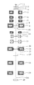
図1の透過型電子顕微鏡は、電子源(1)、例えば熱電界放出源を備えている。電子源(1)の後には、まずその電位によって電子を電子源(1)から吸収する抽出電極(2)と、電子源の位置を光学的に固定するための1つまたは複数の集束電極(3)と、1つまたは複数の陽極(4)とが続く。陽極(4)の電位によって、電子源(1)から出た電子は100KeVまたはそれ以上の所望の電子エネルギーへと加速される。 The transmission electron microscope of FIG. 1 includes an electron source (1), for example, a thermal field emission source. After the electron source (1), first, an extraction electrode (2) that absorbs electrons from the electron source (1) by its potential, and one or more focusing electrodes (for fixing the position of the electron source optically) 3) followed by one or more anodes (4). Depending on the potential of the anode (4), the electrons emitted from the electron source (1) are accelerated to the desired electron energy of 100 KeV or higher.
陽極の後には、電子の移動方向に多段コンデンサが続いている。図示した例示的実施形態では、コンデンサは、3つの個別磁気レンズ(5、6、7)と、コンデンサ−オブジェクティブ−シングルフィールドレンズ(8)からなる入射側部品とを備えている。このようなコンデンサにより、磁気レンズ(5、6、7、8)のレンズ電流を適宜に調整することによって、照明アパーチャと、物体平面(9)の電子ビームによって照射される、コンデンサ−オブジェクティブ−シングルフィールドレンズ(8)の主面における視野が、独立に調整可能である。照明野とアパーチャが異なって照射される場合のコンデンサ内での光線の案内に関しては、米国特許第5,013,913号を参照されたい。したがってここではより詳細に言及する必要はない。もちろん、全体で4段のコンデンサの代わりに、例えば米国特許第6,531,698号に記載のより簡単なコンデンサを設けてもよい。 A multi-stage capacitor follows the anode in the direction of electron movement. In the illustrated exemplary embodiment, the condenser comprises three individual magnetic lenses (5, 6, 7) and an incident side component consisting of a condenser-objective-single field lens (8). With such a condenser, the lens current of the magnetic lens (5, 6, 7, 8) is appropriately adjusted, thereby irradiating with an illumination aperture and an electron beam on the object plane (9). The field of view on the main surface of the field lens (8) can be adjusted independently. See U.S. Pat. No. 5,013,913 for guidance of rays in a condenser when the illumination field and aperture are illuminated differently. Therefore, it is not necessary to mention here in more detail. Of course, a simpler capacitor described in, for example, US Pat. No. 6,531,698 may be provided instead of the four-stage capacitor as a whole.
コンデンサ−オブジェクティブ−シングルフィールドレンズ(8)の前では、前視野が最後のコンデンサ・レンズとして、また後視野が対物レンズとして機能する。物体平面はほぼコンデンサ−オブジェクティブ−シングルフィールドレンズ(8)の磁極片間隙の高さに位置している。物体平面(9)内にはゴニオメーターの形の試料マニピュレータ(図示せず)が配置され、これはコンデンサ−オブジェクティブ−シングルフィールドレンズ(8)の磁極片を貫いている。 In front of the condenser-objective-single field lens (8), the front field serves as the last condenser lens and the back field serves as the objective lens. The object plane is located approximately at the height of the pole piece gap of the condenser-objective-single field lens (8). A sample manipulator (not shown) in the form of a goniometer is arranged in the object plane (9), which penetrates the pole piece of the condenser-objective-single field lens (8).
コンデンサ−オブジェクティブ−シングルフィールドレンズの代わりに、他の対物レンズを設けてもよい。 Other objective lenses may be provided instead of the condenser-objective-single field lens.
コンデンサ−オブジェクティブ−シングルフィールドレンズ(8)の後に、やはり磁気レンズとして形成された第1の回折レンズ(11)が続いている。この第1の回折レンズ(11)はコンデンサ−オブジェクティブ−シングルフィールドレンズ(8)の後焦点面ないしは回折面(10)を拡大して回折中間像面(21)に結像させる。同時に第1の回折レンズ(11)は、物体平面(9)の中間実像(14)を生成する。第1の回折レンズ(11)によって生成される中間像(14)の面内には第1の偏向系(12)が配置されている。この第1の偏向系(12)の後に第2の偏向系が続き、その後に第2の回折レンズ(15)が続く。その際、回折中間像(21)は同時に第2の回折レンズ(15)の主面内またはその近傍に位置している。 The condenser-objective-single field lens (8) is followed by a first diffractive lens (11), also formed as a magnetic lens. The first diffractive lens (11) enlarges the rear focal plane or diffractive surface (10) of the condenser-objective-single field lens (8) and forms an image on the diffractive intermediate image plane (21). At the same time, the first diffractive lens (11) generates an intermediate real image (14) of the object plane (9). A first deflection system (12) is disposed in the plane of the intermediate image (14) generated by the first diffractive lens (11). This first deflection system (12) is followed by a second deflection system, followed by a second diffractive lens (15). At that time, the diffractive intermediate image (21) is simultaneously located in the main surface of the second diffractive lens (15) or in the vicinity thereof.
回折中間像面(21)内には位相板(16)が配置されている。対物レンズの後回折面(10)の像、またはコンデンサ−オブジェクティブ−シングルフィールドレンズ(8)の対物レンズとして機能する後視野の像は、第1の回折レンズ(11)によって生成される結像の結像倍率によって拡大されるので、位相板(16)の直径は、対物レンズの後焦点面(10)の直後の位相板(16)の配置に対して前記結像倍率だけ拡大される。これに対して保持ウエブ(22、27)の幅や環状電極の肉厚のような位相板(16)のその他の寸法は同じ寸法に保つことができ、したがってこれらの構成部品による電極の絞りが全体的に軽減される。 A phase plate (16) is disposed in the diffractive intermediate image plane (21). The image of the back diffractive surface (10) of the objective lens or the image of the back field that functions as the objective lens of the condenser-objective-single field lens (8) is an image of the image generated by the first diffractive lens (11). Since it is enlarged by the imaging magnification, the diameter of the phase plate (16) is enlarged by the imaging magnification relative to the arrangement of the phase plate (16) immediately after the rear focal plane (10) of the objective lens. In contrast, other dimensions of the phase plate (16), such as the width of the retaining webs (22, 27) and the wall thickness of the annular electrode, can be kept the same so that the electrode throttling by these components is reduced. Overall reduction.
回折面(21)が回折中間像面内結像される拡大倍率は2倍より大きく、好ましくは3倍より大きくあるべきである。回折面(21)が回折中間像面内に結像される拡大倍率は、10倍の拡大倍率を超えないものとし、好ましくは3倍の倍率から7倍の倍率の間とする。 The magnification at which the diffractive surface (21) is imaged in the diffractive intermediate image plane should be greater than 2x, preferably greater than 3x. The magnification at which the diffractive surface (21) is imaged in the diffractive intermediate image plane does not exceed 10 times magnification, preferably between 3 times and 7 times magnification.
第2の回折レンズ(15)は、その主面が回折中間像面内またはその近傍に配置されるので、回折中間像面(21)のさらなる結像に影響を及ぼさず、またはさしたる影響を及ぼさない。この第2の回折レンズ(15)は、第1に物体平面(9)の中間像(14)を投影レンズ系(18、19)の入力像面(17)に結像する。それによって後続の物体平面(9)の像面と回折面(10)の適宜に大きな間隔が保証される。投影レンズ系(18、19)は次いで、物体平面(9)内に配置され、投影系(18、19)の入力像面(17)に結像される試料の大きく拡大された像を検出器(20)上に生成する。 Since the main surface of the second diffractive lens (15) is disposed in or near the diffractive intermediate image plane, the second diffractive lens (15) does not affect or has an influence on further imaging of the diffractive intermediate image plane (21). Absent. The second diffractive lens (15) first forms an intermediate image (14) of the object plane (9) on the input image plane (17) of the projection lens system (18, 19). This ensures a reasonably large distance between the image plane of the subsequent object plane (9) and the diffractive surface (10). The projection lens system (18, 19) is then placed in the object plane (9) to detect a greatly magnified image of the sample imaged on the input image plane (17) of the projection system (18, 19). (20) Generate above.
図1で(OA)は全電子光学系の光軸を示している。 In FIG. 1, (OA) indicates the optical axis of the all electron optical system.
第1の回折レンズ(11)と第2の回折レンズ(15)の間の偏向系(12、13)を用いて、対物レンズの後回折面(10)の像の横方向位置を位相板(16)に対して微調整することができる。第1の偏向系は物体平面の中間像(14)が生じる面内に配置され、またはこの面内で作用するので、この第1の偏向系によって行われる偏向は、投影系の入力像面(17)内に生じる物体平面(9)の像の横方向位置に全く影響を及ぼさず、位相板(16)に対する回折像の位置をシフトさせるだけである。 By using a deflection system (12, 13) between the first diffractive lens (11) and the second diffractive lens (15), the lateral position of the image on the rear diffractive surface (10) of the objective lens is changed to a phase plate ( 16) can be finely adjusted. Since the first deflection system is arranged in or acts on the plane in which the intermediate image (14) of the object plane arises, the deflection performed by this first deflection system is the input image plane of the projection system ( 17) The position of the diffracted image relative to the phase plate (16) is merely shifted without affecting the lateral position of the image of the object plane (9) generated in 17).
対物レンズ(8)と第1の投影レンズ(18)の間の前述の結像特性は、図2に光線の経路に基づいて明確に示されている。そこでは、物体平面(9)から光軸(OA)と平行に出射する電子の放射経路、すなわちいわゆる照明光路またはひとみ光路が実線で示され、また光軸(OA)に対して角度をなして物体平面(9)から光軸(OA)上に出射する電子の放射経路、すなわちいわゆる結像光路が破線で示されている。 The aforementioned imaging characteristics between the objective lens (8) and the first projection lens (18) are clearly shown in FIG. 2 on the basis of the ray path. Therein, the radiation path of electrons exiting from the object plane (9) parallel to the optical axis (OA), that is, the so-called illumination optical path or pupil optical path is shown by a solid line, and at an angle to the optical axis (OA). A radiation path of electrons emitted from the object plane (9) onto the optical axis (OA), that is, a so-called imaging optical path is indicated by a broken line.
図3には静電位相板(16)が平面図で示されている。位相板(16)は、丸い穴(26)があいた電子を透過しない外部支持体(21)を有している。穴(26)内には光軸(OA)と同心に中心の環状開口(24)を有する環状電極(23)が配置されている。環状電極(23)は、2つまたは3つの薄い保持ウエブ(22、27)を介して支持体(21)と連結されている。環状電極に静電電位を加えることによって、物体平面(9)で回折されない光線のうち環状開口(24)を通過した近軸光線には位相シフトが加えられ、一方、物体平面でより高次で回折された、または散乱された光線は影響を受けされないままとなる。位相板(16)の構造に関するさらなる詳細については、米国特許第6,797,956号を参照されたい。 FIG. 3 shows a plan view of the electrostatic phase plate (16). The phase plate (16) has an external support (21) that does not transmit electrons with a round hole (26). An annular electrode (23) having a central annular opening (24) concentrically with the optical axis (OA) is disposed in the hole (26). The annular electrode (23) is connected to the support (21) via two or three thin holding webs (22, 27). By applying an electrostatic potential to the annular electrode, a phase shift is applied to the paraxial ray that has passed through the annular aperture (24) among the rays that are not diffracted by the object plane (9), while at higher order in the object plane. Diffracted or scattered light remains unaffected. For further details regarding the structure of the phase plate (16), see US Pat. No. 6,797,956.
第2の回折レンズ(15)の励起の変化によって、このレンズによって行われる像回転により位相板(16)に対する回折像の配向を変更することができる。それによって像の生成にとって重要な、保持ウエブ(22、27)に入射する回折反射光学系(25)は、破線で示した円で示す円形経路を移動し、それによって保持ウエブ(22、27)によって妨げられずに位相板が通過できる領域内に回転することができる。 By changing the excitation of the second diffractive lens (15), the orientation of the diffracted image relative to the phase plate (16) can be changed by image rotation performed by this lens. The diffractive optical system (25) incident on the holding web (22, 27), which is important for image generation, thereby moves in a circular path indicated by a circle indicated by a broken line, and thereby the holding web (22, 27). Can be rotated into an area through which the phase plate can pass without being obstructed by.
図4には、米国特許第6,797,956号に従って円錐形の照明によって位相コントラストを発生する場合の放射経路が示されている。物体平面(49)内で回折されない近軸光線は、対物レンズ(48)の後回折面(50)で合焦され、第1の回折レンズ(51)によって回折中間像面(53)に結像される。回折中間像面(56)の近傍の第1の偏向系(52)が、光束を環状位相板(57)の位相シフト領域を経て環状に回折中間像面(53)へと導く。次いで、主面が回折中間像面(53)内またはその近傍に位置する第2の回折レンズ(58)が、再び物体平面(49)の中間像を第1の投影レンズ(54)の入力像面内に生成する。第1の投影レンズ(54)の入力像面内に配置された、第1の偏向系(52)と同期して動作される別の偏向系(55)によって、第1の投影レンズ(54)の入力像面内の光線を再び光軸に戻るように偏向させる。 FIG. 4 shows the radiation path when phase contrast is generated by conical illumination according to US Pat. No. 6,797,956. The paraxial ray that is not diffracted in the object plane (49) is focused on the rear diffractive surface (50) of the objective lens (48), and formed on the diffractive intermediate image surface (53) by the first diffractive lens (51). Is done. The first deflection system (52) in the vicinity of the diffractive intermediate image plane (56) guides the light beam annularly to the diffractive intermediate image plane (53) through the phase shift region of the annular phase plate (57). Next, the second diffractive lens (58) whose principal surface is located in or near the diffractive intermediate image surface (53) again converts the intermediate image of the object plane (49) into the input image of the first projection lens (54). Generate in-plane. The first projection lens (54) is arranged by another deflection system (55) arranged in the input image plane of the first projection lens (54) and operated in synchronism with the first deflection system (52). Are deflected so as to return to the optical axis again.
回折中間像面(53)内に配置された環状の位相板によって、円形経路を案内される近軸光線に位相シフトが加えられ、一方、位相板の中心開口の縁部から離れて通過する、物体平面(49)内で高い回折次数で回折された電子は、位相板からの影響を受けないままとなる。次いで、このより高次の回折と位相シフトされた近軸光線との干渉によって再び位相コントラストが生ずる。 An annular phase plate disposed in the diffractive intermediate image plane (53) adds a phase shift to the paraxial ray guided through the circular path, while passing away from the edge of the central aperture of the phase plate. Electrons diffracted at a high diffraction order in the object plane (49) remain unaffected by the phase plate. The phase contrast is then again produced by the interference between this higher order diffraction and the phase shifted paraxial ray.
図5の配置は、基本的に図4の配置と同様に構成されている。もちろん、図5の配置は2枚の位相板を有している。第1の位相板(58)は対物レンズの後回折面(15)内に配置され、また第2の位相板(57)は、第2の回折レンズ(53)の主面内またはその近傍に位置しこれと共役する第1の回折レンズ(51)の像面内に配置される。前述の実施形態の場合と同様に、第2の回折レンズは第1と第2の回折レンズ(51、53)の間に位置する、物体平面(49)の単一の中間実像を投影系(54)の入力像面に結像させる。 The arrangement of FIG. 5 is basically the same as the arrangement of FIG. Of course, the arrangement of FIG. 5 has two phase plates. The first phase plate (58) is disposed in the back diffractive surface (15) of the objective lens, and the second phase plate (57) is in the main surface of the second diffractive lens (53) or in the vicinity thereof. It is located in the image plane of the first diffractive lens (51) that is positioned and conjugated with it. As in the previous embodiment, the second diffractive lens projects a single intermediate real image of the object plane (49) located between the first and second diffractive lenses (51, 53) to the projection system ( 54).
両方の位相板(57、58)は、それぞれ異なり互いに相補的な、回折像の空間領域に影響を及ぼすように形成されている。図5に示されているように、対物レンズの回折面(15)内に配置されている位相板(58)は、図5に陰影で示されている光線の円錐セグメント内で位相シフトを生じ、一方、回折中間像面内に配置されている第2の位相板(57)は陰影がない光線円錐セグメント内で位相シフトを生ずる。この場合、位相シフトは互いの共役する2つの回折像内で順次行われ、したがって両方の共同の寄与によって近軸光線と回折光線の間に所望の位相シフトが生じる。この方法によって基本的に、材料不要の、また収差のない静電位相板を実現することが可能になる。その上、両方の位相板(57、58)をそれぞれ、場合によっては存在する保持ウエブが全体として画像生成に悪影響を及ぼさないように形成することができる。散乱電子だけが半平面の位相板によってπの位相シフトを受け、したがって微分的干渉コントラスト(微分干渉コントラスト)を生ずることができる。 Both phase plates (57, 58) are formed so as to influence different spatial regions of the diffraction image which are different from each other and complementary to each other. As shown in FIG. 5, the phase plate (58) arranged in the diffractive surface (15) of the objective lens produces a phase shift in the conical segment of the light beam shown in FIG. On the other hand, the second phase plate (57) arranged in the diffractive intermediate image plane causes a phase shift in the ray cone segment without shadow. In this case, the phase shift is performed sequentially in the two diffracted images that are conjugated to each other, so that the joint contribution of both results in the desired phase shift between the paraxial and diffracted rays. This method basically makes it possible to realize an electrostatic phase plate that requires no material and is free of aberrations. In addition, both phase plates (57, 58) can each be formed such that the existing holding webs as a whole do not adversely affect image generation. Only the scattered electrons are subjected to a π phase shift by the half-plane phase plate, and thus can produce a differential interference contrast (differential interference contrast).
図6には、図1および2を参照して既に記載した実施形態とやや異なる光線案内が示されている。重要な相違は、対物レンズ(60)が、第1の回折レンズ(62)の主面内またはその近傍にも物体平面(61)の中間像を生じるほど強く励起されることである。第1の回折レンズ(62)はやはり対物レンズ(60)の後回折面(65)を第2の回折レンズ(63)の主面内またはその近傍に結像し、したがってやはりそこに回折中間像面が生ずる。そこで回折中間像面内にやはり位相シフト素子(67)が配置される。図2の実施形態と同様に、第2の回折レンズ(63)は、第1の回折レンズの主面内または主面の近傍に生ずる物体平面(61)の中間像を後続の投影系(64)の入力像面(66)に結像する。 FIG. 6 shows a light guide that is slightly different from the embodiment already described with reference to FIGS. The important difference is that the objective lens (60) is excited so strongly that an intermediate image of the object plane (61) is also produced in or near the principal plane of the first diffractive lens (62). The first diffractive lens (62) also forms an image of the rear diffractive surface (65) of the objective lens (60) in or near the main surface of the second diffractive lens (63), and therefore also has a diffractive intermediate image there. A surface arises. Therefore, the phase shift element (67) is also arranged in the diffraction intermediate image plane. Similar to the embodiment of FIG. 2, the second diffractive lens (63) is configured to convert an intermediate image of the object plane (61) generated in or near the main surface of the first diffractive lens to the subsequent projection system (64 ) On the input image plane (66).
図7にはシステムをローレンツ顕微鏡として動作させる場合に、または倍率がより低い場合に実現される光路が示されている。ローレンツ顕微鏡として動作する場合は、対物レンズ(70)がなくされ、倍率がより低い場合(いわゆる低倍率モード)は、対物レンズは極めて弱くしか励起されない。第1の回折レンズ(73)の励起は、その焦点面が第2の回折レンズ(74)の主面内に位置するように選択される。第2の回折レンズの主面内にはやはり位相板(77)が配置される。第2の回折レンズ(74)は、後続の投影系(75)の入力像面(76)内に、第1の回折レンズ(73)によって生成された物体平面(71)の虚像(77)の実像を生成する。次に投影レンズ(75)は物体平面(71)内に位置する物体の10.000倍までに拡大された像を生成する。したがって、この光線案内によって従来の低倍率拡大の約5倍の最高拡大倍率が可能になる。 FIG. 7 shows the optical path that is realized when the system is operated as a Lorentz microscope or when the magnification is lower. When operating as a Lorentz microscope, the objective lens (70) is omitted, and when the magnification is lower (so-called low magnification mode), the objective lens is excited only very weakly. The excitation of the first diffractive lens (73) is selected so that its focal plane is located within the main surface of the second diffractive lens (74). A phase plate (77) is also disposed in the main surface of the second diffractive lens. The second diffractive lens (74) has a virtual image (77) of the object plane (71) generated by the first diffractive lens (73) in the input image plane (76) of the subsequent projection system (75). Generate a real image. Next, the projection lens (75) generates an image magnified to 10.000 times that of the object located in the object plane (71). Therefore, this light guide allows a maximum magnification of about 5 times that of the conventional low magnification magnification.
図2の光線案内で必要な寸法に関しては、ほぼ以下のように見積もることができる。対物レンズ(8)の焦点距離が約3mmで、所望の望遠鏡拡大率が10倍の場合は(対物レンズ(8)と第1の回折レンズ(11)は望遠鏡式に動作されるので)、第1の回折レンズ(11)について約30mmの焦点距離になる。このような望遠鏡系では、対物レンズだけを有するシステムの場合とは異なり、開口収差の増大は無視できる程度である。 The dimensions required for the light guide in FIG. 2 can be estimated as follows. When the focal length of the objective lens (8) is about 3 mm and the desired telescope magnification is 10 times (because the objective lens (8) and the first diffractive lens (11) are operated telescopically), The focal length is about 30 mm for one diffractive lens (11). In such a telescope system, an increase in aperture aberration is negligible unlike a system having only an objective lens.
回折中間像面を対物レンズ(8)の後回折面(10)に比べて約5倍に拡大すべき場合は、第1の回折レンズ(11)は、対物レンズ(8)の後回折面(10)から約36mmの距離でなければならず、第1の回折レンズ(11)と第2の回折レンズ(15)の間には180mmの間隔が必要である。第2の回折レンズ(15)は、第1の回折レンズ(11)の後焦点面(14)に生ずる物体平面(9)の中間像をより低い拡大率で投影系(18)の入射像面(17)に結像するので、第2の回折レンズ(15)の焦点距離が約75mmである場合、第2の回折レンズ(15)と投影系(18)の入力像面(17)の間の必要な間隔は約150mmとなる。その場合、対物レンズ(8)が中間実像を投影系の入力像面内に直接生成する構成の場合よりも全長が約260mm拡大する。 When the diffractive intermediate image plane is to be magnified about 5 times compared to the rear diffractive surface (10) of the objective lens (8), the first diffractive lens (11) has a rear diffractive surface ( The distance from the first diffractive lens (11) to the second diffractive lens (15) is 180 mm. The second diffractive lens (15) is configured to obtain an intermediate image of the object plane (9) generated on the back focal plane (14) of the first diffractive lens (11) with a lower magnification and an incident image plane of the projection system (18). Since the image is formed on (17), when the focal length of the second diffractive lens (15) is about 75 mm, it is between the second diffractive lens (15) and the input image plane (17) of the projection system (18). The required interval is about 150 mm. In that case, the total length is increased by about 260 mm compared to the case where the objective lens (8) is configured to directly generate the intermediate real image in the input image plane of the projection system.
1…電子源、2…抽出電極、3…集束電極、4…陽極、5,6,7…磁気レンズ、8…コンデンサ−オブジェクティブ−シングルフィールドレンズ、9…物体平面、10…回折面、11…回折レンズ、14…中間実像、15…回折レンズ、16…位相板
DESCRIPTION OF
Claims (12)
Applications Claiming Priority (2)
| Application Number | Priority Date | Filing Date | Title |
|---|---|---|---|
| DE102006011615A DE102006011615A1 (en) | 2006-03-14 | 2006-03-14 | Phase contrast electron microscope |
| DE102006011615.1 | 2006-03-14 |
Publications (2)
| Publication Number | Publication Date |
|---|---|
| JP2007250541A JP2007250541A (en) | 2007-09-27 |
| JP5116321B2 true JP5116321B2 (en) | 2013-01-09 |
Family
ID=38283520
Family Applications (1)
| Application Number | Title | Priority Date | Filing Date |
|---|---|---|---|
| JP2007060060A Expired - Fee Related JP5116321B2 (en) | 2006-03-14 | 2007-03-09 | Phase contrast electron microscope |
Country Status (4)
| Country | Link |
|---|---|
| US (3) | US7741602B2 (en) |
| EP (1) | EP1835523B8 (en) |
| JP (1) | JP5116321B2 (en) |
| DE (1) | DE102006011615A1 (en) |
Families Citing this family (28)
| Publication number | Priority date | Publication date | Assignee | Title |
|---|---|---|---|---|
| DE102006055510B4 (en) * | 2006-11-24 | 2009-05-07 | Ceos Corrected Electron Optical Systems Gmbh | Phase plate, image forming method and electron microscope |
| DE102007007923A1 (en) | 2007-02-14 | 2008-08-21 | Carl Zeiss Nts Gmbh | Phase-shifting element and particle beam device with phase-shifting element |
| EP2091062A1 (en) * | 2008-02-13 | 2009-08-19 | FEI Company | TEM with aberration corrector and phase plate |
| EP2131385A1 (en) * | 2008-06-05 | 2009-12-09 | FEI Company | Hybrid phase plate |
| DE102008037698B4 (en) | 2008-08-14 | 2012-08-16 | Carl Zeiss Nts Gmbh | Electron microscope with annular illumination aperture |
| US7977633B2 (en) * | 2008-08-27 | 2011-07-12 | Max-Planck-Gesellschaft Zur Foerderung Der Wissenschaften E. V. | Phase plate, in particular for an electron microscope |
| DE102009001587A1 (en) * | 2009-01-06 | 2010-07-08 | Carl Zeiss Nts Gmbh | Method for adjusting operating parameter of particle radiation device, involves providing sample holder with sample receptacle for receiving reference sample |
| DE102009010774A1 (en) * | 2009-02-26 | 2010-11-11 | Ceos Corrected Electron Optical Systems Gmbh | Method and apparatus for image contrast generation by phase shift |
| NL2004888A (en) * | 2009-06-29 | 2010-12-30 | Asml Netherlands Bv | Deposition method and apparatus. |
| WO2011071819A1 (en) * | 2009-12-07 | 2011-06-16 | Regents Of The University Of California | Optical-cavity phase plate for transmission electron microscopy |
| US8598526B2 (en) | 2010-03-01 | 2013-12-03 | Carl Zeiss Microscopy Gmbh | Transmission electron microscope |
| JP5564292B2 (en) * | 2010-03-05 | 2014-07-30 | 株式会社日立製作所 | Phase plate and phase contrast electron microscope using the same |
| WO2011163397A1 (en) * | 2010-06-22 | 2011-12-29 | The Regents Of The University Of California | Microfabricated high-bandpass foucault aperture for electron microscopy |
| EP2413345B1 (en) * | 2010-07-29 | 2013-02-20 | Carl Zeiss NTS GmbH | Charged particle beam system |
| US20120037815A1 (en) * | 2010-08-16 | 2012-02-16 | Yunn-Shin Shiue | Tem phase plate loading system |
| DE102011011751B4 (en) | 2011-02-18 | 2015-12-17 | Stiftung Caesar Center Of Advanced European Studies And Research | Holding arrangement for holding phase contrast units in a phase-contrast electron microscope and phase-contrast electron microscope |
| DE102011014399B4 (en) | 2011-03-18 | 2017-08-03 | Stiftung Caesar Center Of Advanced European Studies And Research | Phase plate, method for producing a phase plate and electron microscope |
| DE102011113645A1 (en) | 2011-09-19 | 2013-03-21 | Stiftung Caesar Center Of Advanced European Studies And Research | Method for aligning a phase plate in an electron microscope |
| JP6286270B2 (en) | 2013-04-25 | 2018-02-28 | エフ イー アイ カンパニFei Company | Method using a phase plate in a transmission electron microscope |
| DE102013019297A1 (en) | 2013-11-19 | 2015-05-21 | Fei Company | Phase plate for a transmission electron microscope |
| US10170274B2 (en) * | 2015-03-18 | 2019-01-01 | Battelle Memorial Institute | TEM phase contrast imaging with image plane phase grating |
| WO2016149676A1 (en) | 2015-03-18 | 2016-09-22 | Battelle Memorial Institute | Electron beam masks for compressive sensors |
| US10580614B2 (en) | 2016-04-29 | 2020-03-03 | Battelle Memorial Institute | Compressive scanning spectroscopy |
| DE112016006511B4 (en) | 2016-08-22 | 2022-03-24 | Hitachi High-Tech Corporation | Electron microscope and imaging methods |
| US10295677B2 (en) | 2017-05-08 | 2019-05-21 | Battelle Memorial Institute | Systems and methods for data storage and retrieval |
| JP7193694B2 (en) | 2018-07-26 | 2022-12-21 | 国立研究開発法人理化学研究所 | Electron microscope and sample observation method using the same |
| JP7113399B2 (en) * | 2019-03-05 | 2022-08-05 | N-Emラボラトリーズ株式会社 | Electron microscope observation method, aperture scanning high-speed mimicking device for transmission electron microscope, transmission electron microscope and data processing system |
| US11237059B1 (en) * | 2020-12-14 | 2022-02-01 | Gerchberg Ophthalmic Dispensing, PLLC | Totagraphy: Coherent diffractive/digital information reconstruction by iterative phase recovery using special masks |
Family Cites Families (23)
| Publication number | Priority date | Publication date | Assignee | Title |
|---|---|---|---|---|
| DE1049988B (en) * | 1953-09-04 | |||
| US3493287A (en) * | 1966-04-26 | 1970-02-03 | Ibm | Optical detour phase system |
| US3566109A (en) * | 1968-02-15 | 1971-02-23 | Bell Telephone Labor Inc | Electron microscope method and apparatus for improving image phase contrast |
| DE1810818A1 (en) * | 1968-04-16 | 1969-10-23 | Prof Dr Walter Hoppe | Corpuscular beam device with an imaging lens and a phase-shifting film assigned to it |
| CH678663A5 (en) * | 1988-06-09 | 1991-10-15 | Zeiss Carl Fa | |
| DE3825103A1 (en) * | 1988-07-23 | 1990-01-25 | Zeiss Carl Fa | METHOD FOR ILLUMINATING AN OBJECT IN A TRANSMISSION ELECTRON MICROSCOPE |
| JP3703483B2 (en) * | 1993-09-15 | 2005-10-05 | カール−ツァイス−スチフツング | Phase contrast-X-ray microscope |
| JP3400541B2 (en) * | 1994-06-14 | 2003-04-28 | 株式会社日立製作所 | Magnetic microscopic method using scanning electron beam and scanning transmission electron microscope |
| JPH09237603A (en) * | 1995-12-27 | 1997-09-09 | Hitachi Ltd | Phase contrast electron microscope and its phase plate |
| US5814815A (en) * | 1995-12-27 | 1998-09-29 | Hitachi, Ltd. | Phase-contrast electron microscope and phase plate therefor |
| JPH11250850A (en) * | 1998-03-02 | 1999-09-17 | Hitachi Ltd | Scanning electron microscope, microscope method, and interactive input device |
| JP4069545B2 (en) * | 1999-05-19 | 2008-04-02 | 株式会社日立製作所 | Electron microscope method, electron microscope array biological sample inspection method and biological inspection apparatus using the same |
| DE19945344A1 (en) * | 1999-09-22 | 2001-03-29 | Leo Elektronenmikroskopie Gmbh | Particle-optical lighting and imaging system with a condenser-objective single-field lens |
| US6720558B2 (en) * | 2000-02-02 | 2004-04-13 | Jeol Ltd. | Transmission electron microscope equipped with energy filter |
| JP3544914B2 (en) * | 2000-03-17 | 2004-07-21 | 住友化学工業株式会社 | Optical microscope apparatus and microscope observation method. |
| JP3773389B2 (en) * | 2000-03-27 | 2006-05-10 | 日本電子株式会社 | Thin film phase plate for phase contrast electron microscope, phase contrast electron microscope and phase plate antistatic method |
| JP3942363B2 (en) * | 2001-02-09 | 2007-07-11 | 日本電子株式会社 | Lens system for phase plate of transmission electron microscope and transmission electron microscope |
| JP3867524B2 (en) * | 2001-07-05 | 2007-01-10 | 株式会社日立製作所 | Observation apparatus and observation method using electron beam |
| JP4328044B2 (en) * | 2001-09-25 | 2009-09-09 | 日本電子株式会社 | Differential contrast electron microscope and data processing method of electron microscope image |
| DE10200645A1 (en) * | 2002-01-10 | 2003-07-24 | Leo Elektronenmikroskopie Gmbh | Electron microscope with circular illumination aperture |
| WO2005022582A1 (en) * | 2003-09-02 | 2005-03-10 | Nanomegas Sprl | A method for measuring diffraction patterns from a transmission electron microscopy to determine crystal structures and a device therefor |
| DE102007007923A1 (en) * | 2007-02-14 | 2008-08-21 | Carl Zeiss Nts Gmbh | Phase-shifting element and particle beam device with phase-shifting element |
| EP2091062A1 (en) | 2008-02-13 | 2009-08-19 | FEI Company | TEM with aberration corrector and phase plate |
-
2006
- 2006-03-14 DE DE102006011615A patent/DE102006011615A1/en not_active Withdrawn
-
2007
- 2007-02-21 EP EP07102803.9A patent/EP1835523B8/en active Active
- 2007-03-09 JP JP2007060060A patent/JP5116321B2/en not_active Expired - Fee Related
- 2007-03-13 US US11/717,201 patent/US7741602B2/en active Active
-
2010
- 2010-03-19 US US12/659,751 patent/US8039796B2/en active Active
-
2011
- 2011-10-14 US US13/274,066 patent/US8330105B2/en not_active Expired - Fee Related
Also Published As
| Publication number | Publication date |
|---|---|
| EP1835523B8 (en) | 2016-09-28 |
| US20070284528A1 (en) | 2007-12-13 |
| US7741602B2 (en) | 2010-06-22 |
| US20120049062A1 (en) | 2012-03-01 |
| EP1835523A2 (en) | 2007-09-19 |
| US20100181481A1 (en) | 2010-07-22 |
| EP1835523A3 (en) | 2008-03-05 |
| DE102006011615A1 (en) | 2007-09-20 |
| JP2007250541A (en) | 2007-09-27 |
| EP1835523B1 (en) | 2016-06-29 |
| US8039796B2 (en) | 2011-10-18 |
| US8330105B2 (en) | 2012-12-11 |
Similar Documents
| Publication | Publication Date | Title |
|---|---|---|
| JP5116321B2 (en) | Phase contrast electron microscope | |
| JP5147734B2 (en) | Aberration correction cathode lens microscope equipment | |
| JP5871440B2 (en) | Contrast improvement of scanning confocal electron microscope | |
| TWI650550B (en) | Multi-beam device for high throughput ebi | |
| US7507962B2 (en) | Electron-beam device and detector system | |
| US6797956B2 (en) | Electron microscope with annular illuminating aperture | |
| JP5965656B2 (en) | Method for centering an optical element in a TEM comprising an element for improving contrast | |
| JP3942363B2 (en) | Lens system for phase plate of transmission electron microscope and transmission electron microscope | |
| US9613779B2 (en) | Scanning transmission electron microscope with variable axis objective lens and detective system | |
| JP2005276819A (en) | Objective lens for charged particle beam device | |
| JPH11148905A (en) | Electron beam inspection method and apparatus therefor | |
| JP6265643B2 (en) | Electron beam equipment | |
| US10504694B2 (en) | Scanning electron microscope and method of use thereof | |
| JP2022091837A (en) | Particle beam system | |
| JP4354197B2 (en) | Scanning electron microscope | |
| JP2023110072A (en) | Scanning electron microscope and secondary electron detection method for scanning electron microscope | |
| JP2004214111A (en) | Monochromator and scanning electron microscope with monochromator | |
| JP5934513B2 (en) | Transmission electron microscope | |
| US9543115B2 (en) | Electron microscope | |
| JP2007080724A (en) | Magnetic field applying device of electron microscope | |
| JP6636061B2 (en) | Alignment of featureless thin film in TEM | |
| JP2005337959A (en) | Method and device for inspecting substrate | |
| JP2018190731A (en) | Particle source for producing particle beam and particle-optical apparatus | |
| EP3379556B1 (en) | Scanning transmission electron microscope with a condenser objective system and a method of use thereof | |
| JP4792074B2 (en) | Substrate inspection method and substrate inspection apparatus |
Legal Events
| Date | Code | Title | Description |
|---|---|---|---|
| RD03 | Notification of appointment of power of attorney |
Free format text: JAPANESE INTERMEDIATE CODE: A7423 Effective date: 20080730 |
|
| A521 | Written amendment |
Free format text: JAPANESE INTERMEDIATE CODE: A821 Effective date: 20080919 |
|
| RD04 | Notification of resignation of power of attorney |
Free format text: JAPANESE INTERMEDIATE CODE: A7424 Effective date: 20080919 |
|
| A621 | Written request for application examination |
Free format text: JAPANESE INTERMEDIATE CODE: A621 Effective date: 20100217 |
|
| A977 | Report on retrieval |
Free format text: JAPANESE INTERMEDIATE CODE: A971007 Effective date: 20120209 |
|
| A131 | Notification of reasons for refusal |
Free format text: JAPANESE INTERMEDIATE CODE: A131 Effective date: 20120214 |
|
| A521 | Written amendment |
Free format text: JAPANESE INTERMEDIATE CODE: A523 Effective date: 20120511 |
|
| A131 | Notification of reasons for refusal |
Free format text: JAPANESE INTERMEDIATE CODE: A131 Effective date: 20120703 |
|
| A521 | Written amendment |
Free format text: JAPANESE INTERMEDIATE CODE: A523 Effective date: 20120814 |
|
| TRDD | Decision of grant or rejection written | ||
| A01 | Written decision to grant a patent or to grant a registration (utility model) |
Free format text: JAPANESE INTERMEDIATE CODE: A01 Effective date: 20120918 |
|
| A01 | Written decision to grant a patent or to grant a registration (utility model) |
Free format text: JAPANESE INTERMEDIATE CODE: A01 |
|
| A61 | First payment of annual fees (during grant procedure) |
Free format text: JAPANESE INTERMEDIATE CODE: A61 Effective date: 20121016 |
|
| R150 | Certificate of patent or registration of utility model |
Free format text: JAPANESE INTERMEDIATE CODE: R150 Ref document number: 5116321 Country of ref document: JP Free format text: JAPANESE INTERMEDIATE CODE: R150 |
|
| FPAY | Renewal fee payment (event date is renewal date of database) |
Free format text: PAYMENT UNTIL: 20151026 Year of fee payment: 3 |
|
| S111 | Request for change of ownership or part of ownership |
Free format text: JAPANESE INTERMEDIATE CODE: R313111 |
|
| R350 | Written notification of registration of transfer |
Free format text: JAPANESE INTERMEDIATE CODE: R350 |
|
| R250 | Receipt of annual fees |
Free format text: JAPANESE INTERMEDIATE CODE: R250 |
|
| R250 | Receipt of annual fees |
Free format text: JAPANESE INTERMEDIATE CODE: R250 |
|
| R250 | Receipt of annual fees |
Free format text: JAPANESE INTERMEDIATE CODE: R250 |
|
| R250 | Receipt of annual fees |
Free format text: JAPANESE INTERMEDIATE CODE: R250 |
|
| LAPS | Cancellation because of no payment of annual fees |