JP5046521B2 - Light emitting device - Google Patents
Light emitting device Download PDFInfo
- Publication number
- JP5046521B2 JP5046521B2 JP2006010197A JP2006010197A JP5046521B2 JP 5046521 B2 JP5046521 B2 JP 5046521B2 JP 2006010197 A JP2006010197 A JP 2006010197A JP 2006010197 A JP2006010197 A JP 2006010197A JP 5046521 B2 JP5046521 B2 JP 5046521B2
- Authority
- JP
- Japan
- Prior art keywords
- insulating film
- film
- substrate
- light emitting
- conductive film
- Prior art date
- Legal status (The legal status is an assumption and is not a legal conclusion. Google has not performed a legal analysis and makes no representation as to the accuracy of the status listed.)
- Active
Links
- 239000000758 substrate Substances 0.000 claims description 50
- 239000000463 material Substances 0.000 claims description 32
- 229910010272 inorganic material Inorganic materials 0.000 claims description 15
- 239000011147 inorganic material Substances 0.000 claims description 15
- 229920005989 resin Polymers 0.000 claims description 14
- 239000011347 resin Substances 0.000 claims description 14
- 239000003566 sealing material Substances 0.000 claims description 13
- VYPSYNLAJGMNEJ-UHFFFAOYSA-N Silicium dioxide Chemical compound O=[Si]=O VYPSYNLAJGMNEJ-UHFFFAOYSA-N 0.000 claims description 10
- 229910052814 silicon oxide Inorganic materials 0.000 claims description 10
- 239000004642 Polyimide Substances 0.000 claims description 9
- XUIMIQQOPSSXEZ-UHFFFAOYSA-N Silicon Chemical compound [Si] XUIMIQQOPSSXEZ-UHFFFAOYSA-N 0.000 claims description 9
- 229920001721 polyimide Polymers 0.000 claims description 9
- 239000010703 silicon Substances 0.000 claims description 9
- 229910052710 silicon Inorganic materials 0.000 claims description 9
- 229910052581 Si3N4 Inorganic materials 0.000 claims description 8
- HQVNEWCFYHHQES-UHFFFAOYSA-N silicon nitride Chemical compound N12[Si]34N5[Si]62N3[Si]51N64 HQVNEWCFYHHQES-UHFFFAOYSA-N 0.000 claims description 8
- 239000010936 titanium Substances 0.000 claims description 8
- NIXOWILDQLNWCW-UHFFFAOYSA-N acrylic acid group Chemical group C(C=C)(=O)O NIXOWILDQLNWCW-UHFFFAOYSA-N 0.000 claims description 7
- RTAQQCXQSZGOHL-UHFFFAOYSA-N Titanium Chemical compound [Ti] RTAQQCXQSZGOHL-UHFFFAOYSA-N 0.000 claims description 5
- 229910052719 titanium Inorganic materials 0.000 claims description 5
- 229910052782 aluminium Inorganic materials 0.000 claims description 4
- XAGFODPZIPBFFR-UHFFFAOYSA-N aluminium Chemical group [Al] XAGFODPZIPBFFR-UHFFFAOYSA-N 0.000 claims description 4
- 229910052751 metal Inorganic materials 0.000 claims description 4
- 239000002184 metal Substances 0.000 claims description 4
- 150000001408 amides Chemical class 0.000 claims description 3
- 239000012528 membrane Substances 0.000 claims description 3
- ZOKXTWBITQBERF-UHFFFAOYSA-N Molybdenum Chemical compound [Mo] ZOKXTWBITQBERF-UHFFFAOYSA-N 0.000 claims description 2
- 150000001875 compounds Chemical class 0.000 claims description 2
- 239000011733 molybdenum Substances 0.000 claims description 2
- 229910052750 molybdenum Inorganic materials 0.000 claims description 2
- WFKWXMTUELFFGS-UHFFFAOYSA-N tungsten Chemical compound [W] WFKWXMTUELFFGS-UHFFFAOYSA-N 0.000 claims description 2
- 229910052721 tungsten Inorganic materials 0.000 claims description 2
- 239000010937 tungsten Substances 0.000 claims description 2
- 239000004952 Polyamide Substances 0.000 claims 1
- 229920002647 polyamide Polymers 0.000 claims 1
- 239000010408 film Substances 0.000 description 211
- 238000005192 partition Methods 0.000 description 32
- 239000011368 organic material Substances 0.000 description 11
- 238000010586 diagram Methods 0.000 description 10
- 238000007789 sealing Methods 0.000 description 9
- 238000000926 separation method Methods 0.000 description 7
- 239000000945 filler Substances 0.000 description 5
- 239000010410 layer Substances 0.000 description 5
- 238000000034 method Methods 0.000 description 5
- IJGRMHOSHXDMSA-UHFFFAOYSA-N Atomic nitrogen Chemical compound N#N IJGRMHOSHXDMSA-UHFFFAOYSA-N 0.000 description 4
- 239000003990 capacitor Substances 0.000 description 4
- 239000002356 single layer Substances 0.000 description 4
- 239000011521 glass Substances 0.000 description 3
- 229920003023 plastic Polymers 0.000 description 3
- 239000004033 plastic Substances 0.000 description 3
- 229920000915 polyvinyl chloride Polymers 0.000 description 3
- 239000004800 polyvinyl chloride Substances 0.000 description 3
- 229920002620 polyvinyl fluoride Polymers 0.000 description 3
- 239000000565 sealant Substances 0.000 description 3
- XKRFYHLGVUSROY-UHFFFAOYSA-N Argon Chemical compound [Ar] XKRFYHLGVUSROY-UHFFFAOYSA-N 0.000 description 2
- 229920002799 BoPET Polymers 0.000 description 2
- 239000005041 Mylar™ Substances 0.000 description 2
- 239000004962 Polyamide-imide Substances 0.000 description 2
- QVGXLLKOCUKJST-UHFFFAOYSA-N atomic oxygen Chemical compound [O] QVGXLLKOCUKJST-UHFFFAOYSA-N 0.000 description 2
- DQXBYHZEEUGOBF-UHFFFAOYSA-N but-3-enoic acid;ethene Chemical compound C=C.OC(=O)CC=C DQXBYHZEEUGOBF-UHFFFAOYSA-N 0.000 description 2
- 230000001413 cellular effect Effects 0.000 description 2
- KPUWHANPEXNPJT-UHFFFAOYSA-N disiloxane Chemical class [SiH3]O[SiH3] KPUWHANPEXNPJT-UHFFFAOYSA-N 0.000 description 2
- 238000005401 electroluminescence Methods 0.000 description 2
- 239000005038 ethylene vinyl acetate Substances 0.000 description 2
- 239000011152 fibreglass Substances 0.000 description 2
- 229910052757 nitrogen Inorganic materials 0.000 description 2
- 239000001301 oxygen Substances 0.000 description 2
- 229910052760 oxygen Inorganic materials 0.000 description 2
- 229920001200 poly(ethylene-vinyl acetate) Polymers 0.000 description 2
- 229920002312 polyamide-imide Polymers 0.000 description 2
- 229920006267 polyester film Polymers 0.000 description 2
- 229920000642 polymer Polymers 0.000 description 2
- 239000004925 Acrylic resin Substances 0.000 description 1
- 229920000178 Acrylic resin Polymers 0.000 description 1
- 229910052786 argon Inorganic materials 0.000 description 1
- 125000000484 butyl group Chemical group [H]C([*])([H])C([H])([H])C([H])([H])C([H])([H])[H] 0.000 description 1
- 239000000919 ceramic Substances 0.000 description 1
- 239000000428 dust Substances 0.000 description 1
- 239000003822 epoxy resin Substances 0.000 description 1
- 238000005530 etching Methods 0.000 description 1
- 239000011888 foil Substances 0.000 description 1
- 238000010438 heat treatment Methods 0.000 description 1
- 239000011261 inert gas Substances 0.000 description 1
- 239000004973 liquid crystal related substance Substances 0.000 description 1
- 150000002736 metal compounds Chemical class 0.000 description 1
- 150000002739 metals Chemical class 0.000 description 1
- 239000000203 mixture Substances 0.000 description 1
- 239000003960 organic solvent Substances 0.000 description 1
- 230000003071 parasitic effect Effects 0.000 description 1
- 229920000647 polyepoxide Polymers 0.000 description 1
- 230000002250 progressing effect Effects 0.000 description 1
- 230000003252 repetitive effect Effects 0.000 description 1
- 229910001220 stainless steel Inorganic materials 0.000 description 1
- 239000010935 stainless steel Substances 0.000 description 1
- 229920001187 thermosetting polymer Polymers 0.000 description 1
- 239000010409 thin film Substances 0.000 description 1
- XLYOFNOQVPJJNP-UHFFFAOYSA-N water Substances O XLYOFNOQVPJJNP-UHFFFAOYSA-N 0.000 description 1
Images


Classifications
-
- H—ELECTRICITY
- H10—SEMICONDUCTOR DEVICES; ELECTRIC SOLID-STATE DEVICES NOT OTHERWISE PROVIDED FOR
- H10K—ORGANIC ELECTRIC SOLID-STATE DEVICES
- H10K59/00—Integrated devices, or assemblies of multiple devices, comprising at least one organic light-emitting element covered by group H10K50/00
- H10K59/10—OLED displays
- H10K59/12—Active-matrix OLED [AMOLED] displays
- H10K59/131—Interconnections, e.g. wiring lines or terminals
-
- H—ELECTRICITY
- H05—ELECTRIC TECHNIQUES NOT OTHERWISE PROVIDED FOR
- H05B—ELECTRIC HEATING; ELECTRIC LIGHT SOURCES NOT OTHERWISE PROVIDED FOR; CIRCUIT ARRANGEMENTS FOR ELECTRIC LIGHT SOURCES, IN GENERAL
- H05B33/00—Electroluminescent light sources
- H05B33/02—Details
- H05B33/04—Sealing arrangements, e.g. against humidity
-
- H—ELECTRICITY
- H01—ELECTRIC ELEMENTS
- H01L—SEMICONDUCTOR DEVICES NOT COVERED BY CLASS H10
- H01L21/00—Processes or apparatus adapted for the manufacture or treatment of semiconductor or solid state devices or of parts thereof
- H01L21/67—Apparatus specially adapted for handling semiconductor or electric solid state devices during manufacture or treatment thereof; Apparatus specially adapted for handling wafers during manufacture or treatment of semiconductor or electric solid state devices or components ; Apparatus not specifically provided for elsewhere
- H01L21/67005—Apparatus not specifically provided for elsewhere
- H01L21/67011—Apparatus for manufacture or treatment
- H01L21/67126—Apparatus for sealing, encapsulating, glassing, decapsulating or the like
-
- H—ELECTRICITY
- H01—ELECTRIC ELEMENTS
- H01L—SEMICONDUCTOR DEVICES NOT COVERED BY CLASS H10
- H01L23/00—Details of semiconductor or other solid state devices
- H01L23/12—Mountings, e.g. non-detachable insulating substrates
- H01L23/14—Mountings, e.g. non-detachable insulating substrates characterised by the material or its electrical properties
- H01L23/142—Metallic substrates having insulating layers
-
- H—ELECTRICITY
- H01—ELECTRIC ELEMENTS
- H01L—SEMICONDUCTOR DEVICES NOT COVERED BY CLASS H10
- H01L27/00—Devices consisting of a plurality of semiconductor or other solid-state components formed in or on a common substrate
- H01L27/02—Devices consisting of a plurality of semiconductor or other solid-state components formed in or on a common substrate including semiconductor components specially adapted for rectifying, oscillating, amplifying or switching and having potential barriers; including integrated passive circuit elements having potential barriers
- H01L27/12—Devices consisting of a plurality of semiconductor or other solid-state components formed in or on a common substrate including semiconductor components specially adapted for rectifying, oscillating, amplifying or switching and having potential barriers; including integrated passive circuit elements having potential barriers the substrate being other than a semiconductor body, e.g. an insulating body
- H01L27/1214—Devices consisting of a plurality of semiconductor or other solid-state components formed in or on a common substrate including semiconductor components specially adapted for rectifying, oscillating, amplifying or switching and having potential barriers; including integrated passive circuit elements having potential barriers the substrate being other than a semiconductor body, e.g. an insulating body comprising a plurality of TFTs formed on a non-semiconducting substrate, e.g. driving circuits for AMLCDs
-
- H—ELECTRICITY
- H10—SEMICONDUCTOR DEVICES; ELECTRIC SOLID-STATE DEVICES NOT OTHERWISE PROVIDED FOR
- H10K—ORGANIC ELECTRIC SOLID-STATE DEVICES
- H10K50/00—Organic light-emitting devices
- H10K50/10—OLEDs or polymer light-emitting diodes [PLED]
- H10K50/11—OLEDs or polymer light-emitting diodes [PLED] characterised by the electroluminescent [EL] layers
-
- H—ELECTRICITY
- H10—SEMICONDUCTOR DEVICES; ELECTRIC SOLID-STATE DEVICES NOT OTHERWISE PROVIDED FOR
- H10K—ORGANIC ELECTRIC SOLID-STATE DEVICES
- H10K50/00—Organic light-emitting devices
- H10K50/80—Constructional details
- H10K50/84—Passivation; Containers; Encapsulations
- H10K50/842—Containers
- H10K50/8426—Peripheral sealing arrangements, e.g. adhesives, sealants
-
- H—ELECTRICITY
- H10—SEMICONDUCTOR DEVICES; ELECTRIC SOLID-STATE DEVICES NOT OTHERWISE PROVIDED FOR
- H10K—ORGANIC ELECTRIC SOLID-STATE DEVICES
- H10K50/00—Organic light-emitting devices
- H10K50/80—Constructional details
- H10K50/84—Passivation; Containers; Encapsulations
- H10K50/844—Encapsulations
-
- H—ELECTRICITY
- H10—SEMICONDUCTOR DEVICES; ELECTRIC SOLID-STATE DEVICES NOT OTHERWISE PROVIDED FOR
- H10K—ORGANIC ELECTRIC SOLID-STATE DEVICES
- H10K59/00—Integrated devices, or assemblies of multiple devices, comprising at least one organic light-emitting element covered by group H10K50/00
- H10K59/10—OLED displays
- H10K59/12—Active-matrix OLED [AMOLED] displays
- H10K59/121—Active-matrix OLED [AMOLED] displays characterised by the geometry or disposition of pixel elements
- H10K59/1213—Active-matrix OLED [AMOLED] displays characterised by the geometry or disposition of pixel elements the pixel elements being TFTs
-
- H—ELECTRICITY
- H10—SEMICONDUCTOR DEVICES; ELECTRIC SOLID-STATE DEVICES NOT OTHERWISE PROVIDED FOR
- H10K—ORGANIC ELECTRIC SOLID-STATE DEVICES
- H10K59/00—Integrated devices, or assemblies of multiple devices, comprising at least one organic light-emitting element covered by group H10K50/00
- H10K59/80—Constructional details
- H10K59/87—Passivation; Containers; Encapsulations
- H10K59/871—Self-supporting sealing arrangements
- H10K59/8722—Peripheral sealing arrangements, e.g. adhesives, sealants
-
- H—ELECTRICITY
- H10—SEMICONDUCTOR DEVICES; ELECTRIC SOLID-STATE DEVICES NOT OTHERWISE PROVIDED FOR
- H10K—ORGANIC ELECTRIC SOLID-STATE DEVICES
- H10K77/00—Constructional details of devices covered by this subclass and not covered by groups H10K10/80, H10K30/80, H10K50/80 or H10K59/80
- H10K77/10—Substrates, e.g. flexible substrates
-
- H—ELECTRICITY
- H01—ELECTRIC ELEMENTS
- H01L—SEMICONDUCTOR DEVICES NOT COVERED BY CLASS H10
- H01L27/00—Devices consisting of a plurality of semiconductor or other solid-state components formed in or on a common substrate
- H01L27/02—Devices consisting of a plurality of semiconductor or other solid-state components formed in or on a common substrate including semiconductor components specially adapted for rectifying, oscillating, amplifying or switching and having potential barriers; including integrated passive circuit elements having potential barriers
- H01L27/12—Devices consisting of a plurality of semiconductor or other solid-state components formed in or on a common substrate including semiconductor components specially adapted for rectifying, oscillating, amplifying or switching and having potential barriers; including integrated passive circuit elements having potential barriers the substrate being other than a semiconductor body, e.g. an insulating body
- H01L27/1214—Devices consisting of a plurality of semiconductor or other solid-state components formed in or on a common substrate including semiconductor components specially adapted for rectifying, oscillating, amplifying or switching and having potential barriers; including integrated passive circuit elements having potential barriers the substrate being other than a semiconductor body, e.g. an insulating body comprising a plurality of TFTs formed on a non-semiconducting substrate, e.g. driving circuits for AMLCDs
- H01L27/124—Devices consisting of a plurality of semiconductor or other solid-state components formed in or on a common substrate including semiconductor components specially adapted for rectifying, oscillating, amplifying or switching and having potential barriers; including integrated passive circuit elements having potential barriers the substrate being other than a semiconductor body, e.g. an insulating body comprising a plurality of TFTs formed on a non-semiconducting substrate, e.g. driving circuits for AMLCDs with a particular composition, shape or layout of the wiring layers specially adapted to the circuit arrangement, e.g. scanning lines in LCD pixel circuits
- H01L27/1244—Devices consisting of a plurality of semiconductor or other solid-state components formed in or on a common substrate including semiconductor components specially adapted for rectifying, oscillating, amplifying or switching and having potential barriers; including integrated passive circuit elements having potential barriers the substrate being other than a semiconductor body, e.g. an insulating body comprising a plurality of TFTs formed on a non-semiconducting substrate, e.g. driving circuits for AMLCDs with a particular composition, shape or layout of the wiring layers specially adapted to the circuit arrangement, e.g. scanning lines in LCD pixel circuits for preventing breakage, peeling or short circuiting
-
- H—ELECTRICITY
- H10—SEMICONDUCTOR DEVICES; ELECTRIC SOLID-STATE DEVICES NOT OTHERWISE PROVIDED FOR
- H10K—ORGANIC ELECTRIC SOLID-STATE DEVICES
- H10K2102/00—Constructional details relating to the organic devices covered by this subclass
- H10K2102/301—Details of OLEDs
- H10K2102/311—Flexible OLED
-
- H—ELECTRICITY
- H10—SEMICONDUCTOR DEVICES; ELECTRIC SOLID-STATE DEVICES NOT OTHERWISE PROVIDED FOR
- H10K—ORGANIC ELECTRIC SOLID-STATE DEVICES
- H10K59/00—Integrated devices, or assemblies of multiple devices, comprising at least one organic light-emitting element covered by group H10K50/00
- H10K59/80—Constructional details
- H10K59/87—Passivation; Containers; Encapsulations
- H10K59/873—Encapsulations
-
- Y—GENERAL TAGGING OF NEW TECHNOLOGICAL DEVELOPMENTS; GENERAL TAGGING OF CROSS-SECTIONAL TECHNOLOGIES SPANNING OVER SEVERAL SECTIONS OF THE IPC; TECHNICAL SUBJECTS COVERED BY FORMER USPC CROSS-REFERENCE ART COLLECTIONS [XRACs] AND DIGESTS
- Y02—TECHNOLOGIES OR APPLICATIONS FOR MITIGATION OR ADAPTATION AGAINST CLIMATE CHANGE
- Y02E—REDUCTION OF GREENHOUSE GAS [GHG] EMISSIONS, RELATED TO ENERGY GENERATION, TRANSMISSION OR DISTRIBUTION
- Y02E10/00—Energy generation through renewable energy sources
- Y02E10/50—Photovoltaic [PV] energy
- Y02E10/549—Organic PV cells
Landscapes
- Engineering & Computer Science (AREA)
- Physics & Mathematics (AREA)
- Power Engineering (AREA)
- Microelectronics & Electronic Packaging (AREA)
- Condensed Matter Physics & Semiconductors (AREA)
- General Physics & Mathematics (AREA)
- Computer Hardware Design (AREA)
- Optics & Photonics (AREA)
- Manufacturing & Machinery (AREA)
- Geometry (AREA)
- Electroluminescent Light Sources (AREA)
- Devices For Indicating Variable Information By Combining Individual Elements (AREA)
Description
本発明は発光素子を有する発光装置に関する。 The present invention relates to a light emitting device having a light emitting element.
近年、発光材料のEL現象を利用した発光素子(以下、エレクトロルミネッセンス素子、以下「EL素子」という。)を画素に用いた表示装置(エレクトロルミネッセンス表示装置、以下「EL表示装置」という。)の開発が進んでいる。 In recent years, a display device (an electroluminescence display device, hereinafter referred to as an “EL display device”) using a light emitting element (hereinafter referred to as an electroluminescence element, hereinafter referred to as an “EL element”) using an EL phenomenon of a light emitting material as a pixel is used. Development is progressing.
EL素子に用いられる発光性材料には無機発光材料と有機発光材料とがある。有機発光材料は駆動電圧が低いという長所がある。しかし、EL素子に有機材料を用いた有機EL素子は、無機EL素子と比べ水分や酸素の影響を受けやすい。そこで、有機EL表示装置においては、外部から水や酸素などが進入しないように、2つの基板でEL素子を封止している構造が知られている。 The light emitting material used for the EL element includes an inorganic light emitting material and an organic light emitting material. Organic light emitting materials have the advantage of low driving voltage. However, an organic EL element using an organic material for the EL element is more susceptible to moisture and oxygen than an inorganic EL element. Therefore, in an organic EL display device, a structure is known in which EL elements are sealed with two substrates so that water, oxygen and the like do not enter from the outside.
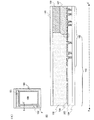
図10に従来のEL表示装置を示す。図10はシール材が設けられる箇所の断面を示す。11、12は基板である。図10は、図面では省略されているがEL素子が設けられた基板である。基板12はEL素子を封止するための封止用の基板である。基板11にはシール材13を設けるためのシール領域14を有する。封止用の基板12はシール材13により基板11に固定される。基板11と基板12の間の空間は樹脂などの充填材15により充填されている。
FIG. 10 shows a conventional EL display device. FIG. 10 shows a cross section of a portion where the sealing material is provided.
16はソースドライバ、ゲートドライバ、FPC端子等から引き回される電源線や信号線などの引き回し配線である。17、18は絶縁膜である。絶縁膜18は画素部において、EL素子の発光材料層を画素ごとに分離するためのものであり、土手、バンク、隔壁と呼ばれるものである。ここでは絶縁膜18を「隔壁」という。隔壁18のシール領域に対応する部分に開口部が形成される。この開口部はシール材13を設けるためのものである。
上記のように隔壁18に開口部を設けると図10(A)に示すように、配線16の側面が隔壁18の端部と重なる部分(点線で囲んだ部分)、図10(B)に示すように配線16の側面と一致したりする部分(点線で囲んだ部分)が多くできる。これらの部分では隔壁18の端部が剥がれやすいということがわかった。基板11から剥がれた隔壁18の端部はごみとなり、画素部に侵入するおそれがある。このような絶縁膜が発光素子に付着すると表示不良となる。
When an opening is provided in the
隔壁18が剥がれる原因として、隔壁18には有機樹脂が用いられるため、配線16に用いられる導電膜との密着性が悪いことにある。特に配線の表面がチタン(Ti)は特に密着性が悪い。
The reason why the
有機樹脂で隔壁18を形成する場合は、シール領域14に開口部を設けた後、水分を抜くための焼成工程があるが、この焼成工程で隔壁18が収縮するため、配線16の段差部分に隔壁の端部がかかっていると、その部分で絶縁膜18が切断されたりして剥がれやすくなる。それは、隔壁18はシール領域14に開口部を設けることで端部が薄くなっているからである。
In the case where the
本発明は、シール領域に隣接する端部で隔壁が剥がれないようにすることを課題とする。 This invention makes it a subject to prevent a partition from peeling in the edge part adjacent to a seal | sticker area | region.
本発明の発光装置は発光素子を有する画素部と、前記画素部を囲む部分に、シール材が形成されたシール領域とを有する第1の基板、および前記第1の基板に前記シール材により固定された第2の基板を有する。 The light-emitting device of the present invention is fixed to the first substrate having a pixel portion having a light-emitting element, a seal region where a seal material is formed in a portion surrounding the pixel portion, and the first substrate with the seal material. A second substrate formed.
本発明において、発光素子はEL素子が用いられる。EL素子としては、無機EL素子、有機EL素子、または無機発光材料と有機発光材料とを混合した発光材料を用いたEL素子のいずれも用いることができる。 In the present invention, an EL element is used as the light emitting element. As the EL element, any of an inorganic EL element, an organic EL element, or an EL element using a light emitting material in which an inorganic light emitting material and an organic light emitting material are mixed can be used.
本発明の発光装置としては、EL表示装置、照明装置などがあげられる。EL表示装置はアクティブ型でもパッシブ型でもよい。また照明装置としては、液晶パネルのバックライトがあげられる。 Examples of the light emitting device of the present invention include an EL display device and a lighting device. The EL display device may be an active type or a passive type. An example of the lighting device is a backlight of a liquid crystal panel.
上記課題を鑑み本発明は、シール領域と隣接する隔壁の端部が駆動回路の配線や引き回し配線などの導電膜と下地が作る段差にかからないようにすることを特徴の1つとする。すなわち、前記第1の基板は、第1の絶縁膜と、前記第1の絶縁膜上の導電膜と、前記導電膜上の第2の絶縁膜を有し、前記第2の絶縁膜は前記シール領域の部分が除去されて、前記シール材が設けられており、前記第2の絶縁膜の前記シール材と隣接している端部は、前記導電膜の側面と上面がつくる段差と重ならないことを特徴とする。 In view of the above problems, one feature of the present invention is that an end portion of a partition wall adjacent to a seal region is not covered with a step formed by a conductive film such as a wiring of a driving circuit or a lead wiring and a base. That is, the first substrate includes a first insulating film, a conductive film on the first insulating film, and a second insulating film on the conductive film, and the second insulating film is The sealing region is removed and the sealing material is provided, and the end of the second insulating film adjacent to the sealing material does not overlap the step formed by the side surface and the top surface of the conductive film. It is characterized by that.
隔壁として機能する第2の絶縁膜は有機樹脂でなる膜であり、例えばアクリル、ポリイミドポリアミド、またはポリイミドアミドである。また、第2の絶縁膜を有機溶媒中に溶かされた絶縁膜材料を塗布した後の熱処理で形成される膜、所謂、塗布珪素酸化膜(Spin on Glass、以下「SOG」ともいう。)を用いることができる。例えば、シロキサンポリマーなどの焼成によりシロキサン結合を形成する材料でなる膜などが挙げられる。 The second insulating film functioning as the partition wall is a film made of an organic resin, such as acrylic, polyimide polyamide, or polyimide amide. In addition, a film formed by heat treatment after applying an insulating film material in which the second insulating film is dissolved in an organic solvent, that is, a so-called coated silicon oxide film (Spin on Glass, hereinafter also referred to as “SOG”). Can be used. For example, a film made of a material that forms a siloxane bond by baking a siloxane polymer or the like can be given.
また本発明は、配線と隔壁となる絶縁膜の間に、隔壁となる絶縁膜と密着性の良い絶縁膜を形成し、配線と絶縁膜が直接接触しないようにすることで、隔壁の剥がれ対策を行う。すなわち、前記第1の基板には、第1の絶縁膜と、前記第1の絶縁膜上の導電膜と、前記導電膜上の第2の絶縁膜と、前記第2の絶縁膜上の第3の絶縁膜が形成されている。前記第3の絶縁膜は前記シール領域の部分が除去されて、前記シール材が設けられており、前記第2の絶縁膜は無機材料でなる膜であり、前記第2の絶縁膜が前記導電膜と接しないように設けられていることを特徴とする。 In addition, the present invention forms an insulating film having good adhesion with the insulating film serving as the partition between the wiring and the insulating film serving as the partition so that the wiring and the insulating film are not in direct contact with each other. I do. That is, the first substrate includes a first insulating film, a conductive film on the first insulating film, a second insulating film on the conductive film, and a second insulating film on the second insulating film. 3 insulating films are formed. The third insulating film is provided with the sealing material by removing a portion of the sealing region, the second insulating film is a film made of an inorganic material, and the second insulating film is the conductive film. It is provided so that it may not contact | connect a film | membrane.
前記無機材料でなる第2の絶縁膜として、酸化珪素膜、窒化珪素膜、酸化窒化珪素膜から選ばれた1つの膜、または複数の膜を積層した膜が用いられる。 As the second insulating film made of the inorganic material, one film selected from a silicon oxide film, a silicon nitride film, and a silicon oxynitride film, or a film in which a plurality of films are stacked is used.
また隔壁として機能する第3の絶縁膜は有機樹脂でなる膜であり、例えばアクリル、ポリイミドポリアミド、またはポリイミドアミドである。また、第2の絶縁膜を、シロキサンポリマーなどの焼成によりシロキサン結合を形成する材料でなる膜のようなSOGも用いられる。 The third insulating film functioning as a partition is a film made of an organic resin, for example, acrylic, polyimide polyamide, or polyimide amide. In addition, SOG such as a film made of a material that forms a siloxane bond by baking a siloxane polymer or the like is used for the second insulating film.
本発明は、隔壁の材料に配線と密着性の良い無機膜を用いることで、隔壁の膜剥がれ対策を行うことを特徴の1つとする。前記第1の基板は、第1の絶縁膜と、前記第1の絶縁膜上の導電膜と、前記導電膜上の無機材料でなる第2の絶縁膜を有し、前記第2の絶縁膜は前記シール領域の部分が除去されて、前記シール材が設けられていることを特徴とする。 One feature of the present invention is to take a countermeasure against film separation of the partition wall by using an inorganic film having good adhesion to the wiring as a material of the partition wall. The first substrate has a first insulating film, a conductive film on the first insulating film, and a second insulating film made of an inorganic material on the conductive film, and the second insulating film Is characterized in that the seal material is provided by removing a portion of the seal region.
隔壁として機能する前記第2の絶縁膜は、酸化珪素膜、窒化珪素膜、酸化窒化珪素膜から選ばれた1つの膜、またはそれらの膜を複数積層した膜である。 The second insulating film functioning as a partition is a film selected from a silicon oxide film, a silicon nitride film, and a silicon oxynitride film, or a film in which a plurality of these films are stacked.
隔壁として機能する絶縁膜の下方に設けられる導電膜は緯線や電極として機能する膜である。この導電膜には、アルミニウム、チタン、モリブデン、タングステン、またはそれら金属の化合物から選ばれた材料でなる膜、またこれらの膜を複数積層した膜が用いられる。 The conductive film provided below the insulating film functioning as a partition wall is a film functioning as a latitude line or an electrode. As the conductive film, a film made of a material selected from aluminum, titanium, molybdenum, tungsten, or a compound of these metals, or a film in which a plurality of these films are stacked is used.
本発明によって、絶縁膜のシール材と隣接している端部が剥がれないようにすることができる。 According to the present invention, it is possible to prevent the end of the insulating film adjacent to the sealing material from being peeled off.
以下に、本発明の実施の形態を図面に基づいて説明する。実施の形態を説明するための全図において、同一部分又は同様な機能を有する部分には同一の符号を付し、その繰り返しの説明は省略する。本発明は多くの異なる態様で実施することが可能であり、本発明の趣旨及びその範囲から逸脱することなくその形態及び詳細を様々に変更し得ることは当業者であれば容易に理解される。従って、本実施の形態の記載内容に限定して解釈されるものではない。 Embodiments of the present invention will be described below with reference to the drawings. Throughout the drawings for describing the embodiments, the same portions or portions having similar functions are denoted by the same reference numerals, and repetitive description thereof is omitted. The present invention can be implemented in many different modes, and it is easily understood by those skilled in the art that modes and details can be variously changed without departing from the spirit and scope of the present invention. . Therefore, the present invention is not construed as being limited to the description of this embodiment mode.
(実施の形態1)
図1(A)は表示装置の上面図を示す。図1(B)は図1(A)のX−X’での断面図を示す。図1(A)に示すように、表示装置は、発光素子を有する画素部100と、駆動回路部としてソースドライバ101およびゲートドライバ102と、画素部100を囲むようにその周囲にシール領域103を有する。シール領域103は封止をするためのシール材が設けられる領域である。ソースドライバ101およびゲートドライバ102は基板104上に設けないものも本実施形態に含む。
(Embodiment 1)
FIG. 1A shows a top view of a display device. FIG. 1B is a cross-sectional view taken along the line XX ′ in FIG. As shown in FIG. 1A, the display device includes a
第1の基板104上に絶縁膜105が設けられている。絶縁膜105には、例えば無機材料の酸化珪素膜、窒化珪素膜、酸化窒化珪素膜などの単層膜、またはこれらの膜の積層膜が用いられる。例えば、組成比の異なる3層の酸化窒化珪素膜が用いられる。
An insulating
絶縁膜105上に導電膜106は、配線や電極として機能する導電膜106が設けられている。導電膜106は、金属、金属化合物の単層膜や積層膜である。例えば材料としてチタン(Ti)、アルミニウム(Al)、チタン(Ti)層からなる膜を用いる。
A
導電膜106上に有機材料の絶縁膜107が形成されている。絶縁膜107は隔壁として機能する膜である。絶縁膜107としては、ポリイミド、アクリルなどの有機樹脂が挙げられる。有機材料の絶縁膜107は、前記第1の透明な膜105との密着性が良いが、導電膜106との密着性は悪い。
An insulating
有機材料の絶縁膜107には、画素部100を囲むシール領域103の部分が選択的に除去されている。シール領域103は、表示装置の大きさや種類、プロセスのルールに従いその都度最適な大きさに形成し、シール材108を形成するのに必要な大きさだけシール領域103として確保する。
A portion of the
第2の基板110は封止用の基板であり、シール領域103に設けられたシール材108により第1の基板104に固定されている。第1の基板104と第2の基板110の密閉空間は有機樹脂などの充墳材109で充墳されている。
The
シール領域103では有機材料の絶縁膜107が除去されている。絶縁膜107のシール領域に隣接する端部が、図10(A)や図10(B)に示すように絶縁膜107の端部が導電膜106の側面にかかったり一致させたりしないようにする。図1(B)に示すように、絶縁膜107の端部は、導電膜106と導電膜106との間の絶縁膜105上に形成される。言い換えると、絶縁膜107の端部は導電膜の側面にかかることなく、絶縁膜105の上面のみに接している。
In the
本実施形態では、導電膜106の側面に有機材料の絶縁膜107の端部がかからないよう配置して、有機材料でなる絶縁膜107の端部からの剥がれを防止するようにした。
In this embodiment, the end of the insulating
図2を用いて、導電膜106と絶縁膜107の位置関係を説明する。図2(A)は、図1(A)のaで示す領域を拡大した図である。図2(B)は、絶縁膜107の端部を説明するための図である。本実施形態は、絶縁膜107の端部すべてが導電膜106上にないことが最も好ましい形態であるが、少なくとも絶縁膜107の端部が導電膜106の側面と上面で作る段差にかからないにすることにある。絶縁膜107の端部は膜厚が非常に薄いので、端部が導電膜106との段差にかからないようにすることで、端部が剥がれることを防ぐものである。
The positional relationship between the
図2(B)を用いて絶縁膜107の端部について説明する。本実施形態では、絶縁膜107の端部とは、シール領域103の境界(シール材108と接している先端)からの幅Wが0.5μmの領域200をいう。あるいは、絶縁膜107の端部とは、シール領域103の境界から膜厚dが42nm以下の領域200をいう。また、絶縁膜の端部をシール領域103の境界から膜厚dが50nm以下の領域とするほうが、端部からの剥がれを防止する点ではより好ましい。本実施形態では、絶縁膜107の端部200とは、上記のように、絶縁膜107の先端からの幅W又は膜厚dのいずれかで決定される領域である。他の実施形態についても絶縁膜107の端部は同様の領域をいう。
An end portion of the insulating
本実施形態では、絶縁膜107の端部200が導電膜107の段差にかからないよう設ける。別の言い方をすると、絶縁膜107の端部全体が導電膜107の上面に位置するか、導電膜107の下地部分の絶縁膜105上面に位置するように設ける。図2(A)に示すように、例えば、絶縁膜107の端部200aでは下地は絶縁膜105の上面であり、絶縁膜107の端部200bでは導電膜106の上面である。端部200a、端部200bは代表的に示したものであるが、本実施形態では、シール領域103と隣接する部分において絶縁膜107の端部200は、端部200a、200bと同様に、導電膜106の上面のみまたは絶縁膜105の上面のみに配置される。
In this embodiment, the
(実施の形態2)
本実施の形態では、絶縁膜の端部での剥がれを、配線と隔壁を直接接触させないようにすることで対策する方法について記載する。図3(A)は表示装置の上面図を示す。図3(B)は図1(A)のY−Y’での断面図を示している。本実施形態では、シール領域103の表面を無機材料でなる絶縁膜300で覆うものである。
(Embodiment 2)
In this embodiment mode, a method for preventing peeling at an end portion of an insulating film by preventing direct contact between a wiring and a partition wall is described. FIG. 3A is a top view of the display device. FIG. 3B is a cross-sectional view taken along line YY ′ of FIG. In the present embodiment, the surface of the
本実施形態では、導電膜106を覆って、基板104全体に無機材料でなる絶縁膜300が設けられる。無機材料でなる絶縁膜300として、例えば材料として酸化珪素膜、窒化珪素膜、酸化珪素膜などが用いられる。図4(A)に示すように、導電膜106の端部が絶縁膜107と重なっていたり、図4(B)に示すように絶縁膜107の端部と一致したりしていても、導電膜106と有機材料の絶縁膜107の間には、有機材料と密着性の良い無機材料でなる絶縁膜300を有するため、有機材料の絶縁膜107が剥がれることを防止できる。よって本実施形態では、導電膜106のレイアウトやシール領域103のレイアウトの自由度が広がる。
In this embodiment, an insulating
(実施の形態3)
本実施の形態では、絶縁膜の端部での剥がれを、隔壁となる絶縁膜の材料を変えることにより対策する方法について記載する。
(Embodiment 3)
In this embodiment mode, a method for dealing with peeling at an end portion of an insulating film by changing a material of the insulating film to be a partition is described.
図5(A)は表示装置の上面図を示す。図5(B)は図5(A)のZ−Z’での断面図を示している。 FIG. 5A is a top view of the display device. FIG. 5B is a cross-sectional view taken along the line Z-Z ′ in FIG.
本実施形態では、有機材料でなる絶縁膜107の代わりに、無機材料でなる絶縁膜500を設ける。図5(B)に示すように絶縁膜500の端部を導電膜106と106の間に設けている。絶縁膜500は、酸化珪素膜、窒化珪素膜、酸化窒化珪素膜の単層膜またはこれらの積層膜を用いることができる。
In this embodiment, an insulating
絶縁膜500を無機材料とすることで、無機材料の絶縁膜105および導電膜106との密着性が改善される。よって、導電膜106のレイアウトの自由度が高まり、導電膜106の端部が絶縁膜500の端部と重ねる、絶縁膜500の端部と一致してもよい。無機物の絶縁膜500は導電膜106と密着性が良いため無機物の絶縁膜500が剥がれるのを防止することが可能である。また、導電膜106のレイアウトやシール領域103のレイアウトの自由度が広がる。
By using the insulating
本実施例は、本発明をEL表示装置に適用した例である。図6を用いて本実施例を説明する。図6(A)は、第1の基板上に形成されたTFT及び発光素子を、第2の基板との間にシール材によって封止した、パネルの上面図であり、図6(B)は、図6(A)のA−A’における断面図に相当する。 In this embodiment, the present invention is applied to an EL display device. The present embodiment will be described with reference to FIG. 6A is a top view of a panel in which a TFT and a light-emitting element formed over a first substrate are sealed with a sealing material between the second substrate and FIG. 6B. This corresponds to a cross-sectional view taken along the line AA ′ of FIG.
第1の基板4001上には画素部4002と、ソースドライバ4003と、ゲートドライバ4004が設けられており、画素部を囲むようにして、シール材4005が設けられている。また画素部4002上には、シール材4005を介して、第2の基板4006が設けられている。画素部4002と、ソースドライバ4003と、ゲートドライバ4004とは、第1の基板4001とシール材4005と第2の基板4006とによって、充填材4007と共に封止されている。
A
第1の基板4001、第2の基板4006としては、ガラス、金属(代表的にはステンレス)、セラミックス、プラスチックを用いることができる。プラスチックとしては、FRP(Fiberglass−Reinforced Plastics)板、PVF(ポリビニルフルオライド)フィルム、マイラーフィルム、ポリエステルフィルムまたはアクリル樹脂フィルムを用いることができる。また、アルミニウムホイルをPVFフィルムやマイラーフィルムで挟んだ構造のシートを用いることもできる。発光素子4011からの光の取り出し方向に位置する基板は透光性を有していなければならない。その場合には、ガラス板、プラスチック板、ポリエステルフィルムまたはアクリルフィルムのような透光性を有する材料を用いる。
As the
充填材4007としては窒素やアルゴンなどの不活性な気体の他に、紫外線硬化樹脂または熱硬化樹脂を用いることができ、PVC(ポリビニルクロライド)、アクリル、ポリイミド、エポキシ樹脂、シリコン樹脂、PVB(ポリビニルブチラル)またはEVA(エチレンビニルアセテート)を用いることができる。本実施例では充填材として窒素を用いる。
As the
第1の基板4001上に設けられた画素部4002と、ソースドライバ4003と、ゲートドライバ4004とは、薄膜トランジスタ(TFT)を複数有しており、図6(B)では、ソースドライバ4003に含まれるTFT4008と、画素部4002に含まれるTFT4009とを例示している。
The
4011は発光素子に相当し、TFT4009のドレインと接続されている配線4017の一部が、発光素子4011の第1の電極として機能する。透明導電膜4012が、発光素子4011の第2の電極として機能する。第1の電極と第2の電極の間に発光材料を含む発光層4013を有する。なお、発光素子4011の構成は、本実施例に示した構成に限定されない。上記実施例のように、発光素子4011から取り出す光の方向や、TFT4009の極性などに合わせて、発光素子4011の構成は適宜変えることができる。発光素子4011から取り出す光の方向は、第1の基板4001側と、第2の基板4006側と、第1の基板4001側及び第2の基板4006側とがある。
ソースドライバ4003、ゲートドライバ4004または画素部4002に与えられる各種信号及び電圧は、図6(B)に示す断面図では図示されていないが、引き回された電源線4014及び4015を介して、FPC端子4016から供給されている。
Various signals and voltages supplied to the
本実施例では、FPC端子4016が、発光素子4011の第1の電極と同じ導電膜から形成されている。また、電源線4014は、配線4017と同じ導電膜から形成されている。また電源線4015はTFT4009およびTFT4008のゲートと同じ導電膜から形成されている。
In this embodiment, the
FPC端子4016は、FPC4018が有する端子と、異方性導電膜4019を介して電気的に接続されている。
The
絶縁膜4022はポリイミド、アクリル、ポリイミドアミドなどの有機樹脂材料であり、絶縁膜4021は酸化珪素膜、窒化珪素膜、酸化窒化珪素膜などの無機材料でなる膜の単層膜や積層膜が用いられる。
The insulating
絶縁膜4022は、発光素子4011の発光層4013を画素ごとに分離するための絶縁膜であり、第1の基板4001全体に形成されている。絶縁膜4022には、発光素子4011が形成される領域、およびシール領域4020がエッチングにより選択的に除去されて、開口部が形成されている。後者の開口部は図6(B)に示すように、シール領域4020において電源線4014に代表出される導電膜の端部は、絶縁膜4022の端部がかかったり、一致したりしないように形成される。その結果、絶縁膜4020の端部は、密着性の良い無機材料でなる絶縁膜4021と接触しているので、有機材料の絶縁膜4022の端部からの剥がれを防止することができる。
The insulating
本実施例では、実施例1の画素部の回路について説明する。なお、本発明の画素回路は、本実施例で示した回路に限定されるものではない。
In this embodiment, a circuit of a pixel portion in
図7は、画素の等価回路図の一例を示したものである。信号線6114、電源線6115、走査線6116、発光素子6113、トランジスタ6110、6111、容量素子6112を有する。信号線6114にはソースドライバによってビデオ信号が入力される。トランジスタ6110は、走査線6116に入力される選択信号に従って、トランジスタ6111のゲートへの、該ビデオ信号の電位の供給を制御することができる。トランジスタ6111は、該ビデオ信号の電位に従って、発光素子6113への電流の供給を制御することができる。容量素子6112は、トランジスタ6111のゲート・ソース間の電圧を保持することができる。なお、図7では、容量素子6112を図示したが、トランジスタ6111のゲート容量や他の寄生容量で賄うことが可能な場合には、設けなくてもよい。
FIG. 7 shows an example of an equivalent circuit diagram of a pixel. A
図8(A)は、図7に示した画素に、トランジスタ6118と走査線6119を新たに設けた画素の等価回路図である。トランジスタ6118により、トランジスタ6111のゲートとソースを同電位とし、強制的に発光素子6113に電流が流れない状態を作ることができるため、全ての画素にビデオ信号が入力される期間よりも、サブフレーム期間の長さを短くすることができる。従って、駆動周波数を抑えつつ、高い総階調数の表示を行うときに、好適である。
FIG. 8A is an equivalent circuit diagram of a pixel in which a
図8(B)は、図8(A)に示した画素に、新たにトランジスタ6125と、配線6126を設けた画素の等価回路図である。トランジスタ6125は、そのゲートの電位が、配線6126によって固定されている。そして、トランジスタ6111とトランジスタ6125は、電源線6115と発光素子6113との間に直列に接続されている。よって図8(B)では、トランジスタ6125により発光素子6113に供給される電流の値が制御され、トランジスタ6111により発光素子6113への該電流の供給の有無が制御できる。
FIG. 8B is an equivalent circuit diagram of a pixel in which a
本発明を適用したEL表示装置は、バッテリー駆動する電子機器の表示部や、大画面の表示装置や、電子機器の表示部に好適に用いることができる。例えば、テレビジョン装置(テレビ、テレビジョン受信機)、デジタルカメラ、デジタルビデオカメラ、携帯電話装置(携帯電話機)、PDA等の携帯情報端末、携帯型ゲーム機、モニター、コンピュータ、カーオーディオ等の音響再生装置、家庭用ゲーム機等の記録媒体を備えた画像再生装置等が挙げられる。その具体例について、図9を参照して説明する。 An EL display device to which the present invention is applied can be suitably used for a display unit of a battery-driven electronic device, a large-screen display device, or a display unit of an electronic device. For example, the sound of a television device (television, television receiver), digital camera, digital video camera, mobile phone device (mobile phone), PDA or other portable information terminal, portable game machine, monitor, computer, car audio, etc. Examples thereof include an image reproducing device provided with a recording medium such as a reproducing device and a home game machine. A specific example will be described with reference to FIG.
図9(A)に示す携帯情報端末機器は、本体9201、表示部9202等を含んでいる。表示部9202は、本発明の表示装置を適用することができる。その結果、隔壁の膜剥がれを防止した携帯情報端末機器を提供することができる。
A portable information terminal device illustrated in FIG. 9A includes a
図9(B)に示すデジタルビデオカメラは、表示部9701、表示部9702等を含んでいる。表示部9701は本発明の表示装置を適用することができる。その結果隔壁の膜剥がれを防止したデジタルビデオカメラを提供することができる。
A digital video camera shown in FIG. 9B includes a
図9(C)に示す携帯電話機は、本体9101、表示部9102等を含んでいる。表示部9102は、本発明の表示装置を適用することができる。その結果、隔壁の膜剥がれを防止した携帯電話機を提供することができる。
A cellular phone shown in FIG. 9C includes a
図9(D)に示す携帯型のテレビジョン装置は、本体9301、表示部9302等を含んでいる。表示部9302は、本発明の表示装置を適用することができる。その結果、隔壁の膜剥がれを防止した携帯型のテレビジョン装置を提供することができる。またテレビジョン装置としては、携帯電話機などの携帯端末に搭載する小型のものから、持ち運びをすることができる中型のもの、また、大型のもの(例えば40インチ以上)まで、幅広いものに、本発明の表示装置を適用することができる。
A portable television device illustrated in FIG. 9D includes a
図9(E)に示す携帯型のコンピュータは、本体9401、表示部9402等を含んでいる。表示部9402は、本発明の表示装置を適用することができる。その結果、隔壁の膜剥がれを防止した携帯型のコンピュータを提供することができる。
A portable computer shown in FIG. 9E includes a
図9(F)に示すテレビジョン装置は、本体9501、表示部9502等を含んでいる。表示部9502は、本発明の表示装置を適用することができる。その結果、隔壁の膜剥がれを防止したテレビジョン装置を提供することができる。
A television device illustrated in FIG. 9F includes a
100 画素部
101 ソースドライバ
102 ゲートドライバ
103 シール領域
104 第1の基板
105 第1の絶縁膜
106 導電膜
107 第2の絶縁膜
108 シール材
109 充填材
110 第2の基板
100
Claims (6)
前記第1の基板には、第1の絶縁膜と、前記第1の絶縁膜上の導電膜と、前記導電膜上の無機材料でなる第2の絶縁膜と、前記第2の絶縁膜上の有機樹脂でなる第3の絶縁膜が形成され、
前記シール領域は前記第3の絶縁膜が除去されており、
前記シール材は前記第2の絶縁膜上に接して設けられ、
前記第2の絶縁膜は、前記第3の絶縁膜が前記導電膜と接しないように設けられていることを特徴とする発光装置。 A first substrate having a pixel portion having a light emitting element, a seal region in which a seal material is formed in a portion surrounding the pixel portion, and a second substrate fixed to the first substrate by the seal material Have
The first substrate includes a first insulating film, a conductive film on the first insulating film, a second insulating film made of an inorganic material on the conductive film, and on the second insulating film. A third insulating film made of an organic resin is formed,
The seal region has the third insulating film removed;
The sealing material is provided on and in contact with the second insulating film;
The light-emitting device, wherein the second insulating film is provided so that the third insulating film is not in contact with the conductive film.
前記第1の基板には、第1の絶縁膜と、導電膜と、無機材料でなる第2の絶縁膜と、有機樹脂でなる第3の絶縁膜が形成され、
前記導電膜は前記第1の絶縁膜上に接して設けられ、
前記第2の絶縁膜は前記第1の絶縁膜及び前記導電膜上に接して設けられ、
前記第3の絶縁膜は前記第2の絶縁膜上に接して設けられ、
前記シール領域は前記第3の絶縁膜が除去されており、
前記シール材は前記第2の絶縁膜上に接して設けられ、
前記第2の絶縁膜は、前記第3の絶縁膜が前記導電膜と接しないように設けられていることを特徴とする発光装置。 A first substrate having a pixel portion having a light emitting element, a seal region in which a seal material is formed in a portion surrounding the pixel portion, and a second substrate fixed to the first substrate by the seal material Have
A first insulating film, a conductive film, a second insulating film made of an inorganic material, and a third insulating film made of an organic resin are formed on the first substrate,
The conductive film is provided on and in contact with the first insulating film;
The second insulating film is provided on and in contact with the first insulating film and the conductive film,
The third insulating film is provided on and in contact with the second insulating film;
The seal region has the third insulating film removed;
The sealing material is provided on and in contact with the second insulating film;
The light-emitting device, wherein the second insulating film is provided so that the third insulating film is not in contact with the conductive film.
Priority Applications (8)
| Application Number | Priority Date | Filing Date | Title |
|---|---|---|---|
| JP2006010197A JP5046521B2 (en) | 2006-01-18 | 2006-01-18 | Light emitting device |
| US11/652,487 US7812524B2 (en) | 2006-01-18 | 2007-01-12 | Light emitting device |
| KR20070004225A KR101495887B1 (en) | 2006-01-18 | 2007-01-15 | Light emitting device |
| US12/874,372 US8283859B2 (en) | 2006-01-18 | 2010-09-02 | Light emitting device |
| US13/612,249 US8710734B2 (en) | 2006-01-18 | 2012-09-12 | Light emitting device |
| KR1020130086375A KR101469935B1 (en) | 2006-01-18 | 2013-07-22 | Light emitting device |
| US14/256,660 US9356048B2 (en) | 2006-01-18 | 2014-04-18 | Light emitting device |
| US15/162,667 US9704940B2 (en) | 2006-01-18 | 2016-05-24 | Light emitting device |
Applications Claiming Priority (1)
| Application Number | Priority Date | Filing Date | Title |
|---|---|---|---|
| JP2006010197A JP5046521B2 (en) | 2006-01-18 | 2006-01-18 | Light emitting device |
Publications (3)
| Publication Number | Publication Date |
|---|---|
| JP2007194040A JP2007194040A (en) | 2007-08-02 |
| JP2007194040A5 JP2007194040A5 (en) | 2009-03-05 |
| JP5046521B2 true JP5046521B2 (en) | 2012-10-10 |
Family
ID=38262551
Family Applications (1)
| Application Number | Title | Priority Date | Filing Date |
|---|---|---|---|
| JP2006010197A Active JP5046521B2 (en) | 2006-01-18 | 2006-01-18 | Light emitting device |
Country Status (3)
| Country | Link |
|---|---|
| US (5) | US7812524B2 (en) |
| JP (1) | JP5046521B2 (en) |
| KR (2) | KR101495887B1 (en) |
Families Citing this family (15)
| Publication number | Priority date | Publication date | Assignee | Title |
|---|---|---|---|---|
| JP5046521B2 (en) * | 2006-01-18 | 2012-10-10 | 株式会社半導体エネルギー研究所 | Light emitting device |
| US7863612B2 (en) | 2006-07-21 | 2011-01-04 | Semiconductor Energy Laboratory Co., Ltd. | Display device and semiconductor device |
| JP4623068B2 (en) * | 2007-09-12 | 2011-02-02 | ソニー株式会社 | Display panel, display panel module, and electronic device |
| KR101953724B1 (en) * | 2011-08-26 | 2019-03-04 | 가부시키가이샤 한도오따이 에네루기 켄큐쇼 | Light-emitting module, light-emitting device, method of manufacturing the light-emitting module, and method of manufacturing the light-emitting device |
| JP6142151B2 (en) | 2012-07-31 | 2017-06-07 | 株式会社Joled | Display device and electronic device |
| KR102052746B1 (en) * | 2013-07-29 | 2019-12-06 | 엘지디스플레이 주식회사 | Face Sealing Type Ogranic Light Emitting Diode Display |
| KR102360783B1 (en) * | 2014-09-16 | 2022-02-10 | 삼성디스플레이 주식회사 | display device |
| TWI606771B (en) * | 2015-04-01 | 2017-11-21 | 群創光電股份有限公司 | Display panel |
| KR102451728B1 (en) * | 2015-05-19 | 2022-10-07 | 삼성디스플레이 주식회사 | Organic light-emitting display apparatus and manufacturing the same |
| WO2017131078A1 (en) * | 2016-01-28 | 2017-08-03 | シャープ株式会社 | Active matrix substrate and method for manufacturing same |
| CN109243305B (en) * | 2018-09-17 | 2021-10-12 | 京东方科技集团股份有限公司 | Display panel, display device, and method for manufacturing display panel |
| CN111370439A (en) | 2018-12-07 | 2020-07-03 | 京东方科技集团股份有限公司 | Display panel, preparation method thereof and display device |
| CN109728195B (en) * | 2018-12-29 | 2021-05-18 | 厦门天马微电子有限公司 | Display panel and display device |
| KR20210044362A (en) * | 2019-10-14 | 2021-04-23 | 삼성디스플레이 주식회사 | Display device and method for manufacturing the same |
| CN113867053B (en) * | 2020-06-30 | 2023-05-16 | 京东方科技集团股份有限公司 | Display panel and preparation method thereof |
Family Cites Families (26)
| Publication number | Priority date | Publication date | Assignee | Title |
|---|---|---|---|---|
| US6288764B1 (en) * | 1996-06-25 | 2001-09-11 | Semiconductor Energy Laboratory Co., Ltd. | Display device or electronic device having liquid crystal display panel |
| TWI264244B (en) * | 2001-06-18 | 2006-10-11 | Semiconductor Energy Lab | Light emitting device and method of fabricating the same |
| US6947921B2 (en) | 2001-07-03 | 2005-09-20 | Eastman Kodak Company | Method and system for capturing memories of deceased individuals |
| JP3674848B2 (en) * | 2001-10-31 | 2005-07-27 | 富士電機ホールディングス株式会社 | Organic thin film light emitting display and method for manufacturing the same |
| JP3724725B2 (en) * | 2001-11-01 | 2005-12-07 | ソニー株式会社 | Manufacturing method of display device |
| US6822264B2 (en) * | 2001-11-16 | 2004-11-23 | Semiconductor Energy Laboratory Co., Ltd. | Light emitting device |
| EP1369499A3 (en) | 2002-04-15 | 2004-10-20 | Semiconductor Energy Laboratory Co., Ltd. | Method of fabricating light-emitting device and apparatus for manufacturing light-emitting device |
| JP4391126B2 (en) * | 2002-05-15 | 2009-12-24 | 株式会社半導体エネルギー研究所 | Method for manufacturing light emitting device |
| TWI263339B (en) * | 2002-05-15 | 2006-10-01 | Semiconductor Energy Lab | Light emitting device and method for manufacturing the same |
| JP4240276B2 (en) * | 2002-07-05 | 2009-03-18 | 株式会社半導体エネルギー研究所 | Light emitting device |
| CN100466285C (en) | 2002-09-11 | 2009-03-04 | 株式会社半导体能源研究所 | Light-emitting apparatus and fabrication method of the same |
| JP3915734B2 (en) * | 2003-05-12 | 2007-05-16 | ソニー株式会社 | Vapor deposition mask, display device manufacturing method using the same, and display device |
| US7161184B2 (en) | 2003-06-16 | 2007-01-09 | Semiconductor Energy Laboratory Co., Ltd. | Display device and method for manufacturing the same |
| SG142140A1 (en) | 2003-06-27 | 2008-05-28 | Semiconductor Energy Lab | Display device and method of manufacturing thereof |
| US7816863B2 (en) * | 2003-09-12 | 2010-10-19 | Semiconductor Energy Laboratory Co., Ltd. | Light emitting device and method for manufacturing the same |
| JP3915806B2 (en) * | 2003-11-11 | 2007-05-16 | セイコーエプソン株式会社 | Electro-optical device and electronic apparatus |
| JP4131243B2 (en) * | 2004-02-06 | 2008-08-13 | セイコーエプソン株式会社 | Electro-optical device manufacturing method, electro-optical device, and electronic apparatus |
| KR100615212B1 (en) | 2004-03-08 | 2006-08-25 | 삼성에스디아이 주식회사 | Flat display device |
| US7183147B2 (en) * | 2004-03-25 | 2007-02-27 | Semiconductor Energy Laboratory Co., Ltd. | Light emitting device, method for manufacturing thereof and electronic appliance |
| US7202504B2 (en) * | 2004-05-20 | 2007-04-10 | Semiconductor Energy Laboratory Co., Ltd. | Light-emitting element and display device |
| JP2005340020A (en) * | 2004-05-27 | 2005-12-08 | Hitachi Displays Ltd | Organic electroluminescent display device and manufacturing method of the same |
| US7550769B2 (en) * | 2004-06-11 | 2009-06-23 | Semiconductor Energy Laboratory Co., Ltd. | Light emitting element, light emitting device and semiconductor device |
| US8217396B2 (en) * | 2004-07-30 | 2012-07-10 | Semiconductor Energy Laboratory Co., Ltd. | Display device comprising electrode layer contacting wiring in the connection region and extending to pixel region |
| US20060250078A1 (en) * | 2005-05-09 | 2006-11-09 | City University Of Hong Kong | Organic electroluminescent devices incorporating UV-illuminated fluorocarbon layers |
| US7838347B2 (en) | 2005-08-12 | 2010-11-23 | Semiconductor Energy Laboratory Co., Ltd. | Display device and manufacturing method of display device |
| JP5046521B2 (en) * | 2006-01-18 | 2012-10-10 | 株式会社半導体エネルギー研究所 | Light emitting device |
-
2006
- 2006-01-18 JP JP2006010197A patent/JP5046521B2/en active Active
-
2007
- 2007-01-12 US US11/652,487 patent/US7812524B2/en not_active Expired - Fee Related
- 2007-01-15 KR KR20070004225A patent/KR101495887B1/en active IP Right Grant
-
2010
- 2010-09-02 US US12/874,372 patent/US8283859B2/en active Active
-
2012
- 2012-09-12 US US13/612,249 patent/US8710734B2/en active Active
-
2013
- 2013-07-22 KR KR1020130086375A patent/KR101469935B1/en active IP Right Grant
-
2014
- 2014-04-18 US US14/256,660 patent/US9356048B2/en active Active
-
2016
- 2016-05-24 US US15/162,667 patent/US9704940B2/en active Active
Also Published As
| Publication number | Publication date |
|---|---|
| US20100327739A1 (en) | 2010-12-30 |
| US8283859B2 (en) | 2012-10-09 |
| US7812524B2 (en) | 2010-10-12 |
| KR20070076481A (en) | 2007-07-24 |
| US9704940B2 (en) | 2017-07-11 |
| US8710734B2 (en) | 2014-04-29 |
| KR20130098945A (en) | 2013-09-05 |
| KR101469935B1 (en) | 2014-12-08 |
| US20160268365A1 (en) | 2016-09-15 |
| US9356048B2 (en) | 2016-05-31 |
| US20070164675A1 (en) | 2007-07-19 |
| US20140306228A1 (en) | 2014-10-16 |
| US20130001608A1 (en) | 2013-01-03 |
| JP2007194040A (en) | 2007-08-02 |
| KR101495887B1 (en) | 2015-02-25 |
Similar Documents
| Publication | Publication Date | Title |
|---|---|---|
| JP5046521B2 (en) | Light emitting device | |
| EP3163646B1 (en) | Organic light emitting display device | |
| EP3098869B1 (en) | Display device | |
| US10431769B2 (en) | Organic light emitting display device | |
| JP5299475B2 (en) | Display device and electronic device | |
| TW538246B (en) | Display panel, display panel inspection method, and display panel manufacturing method | |
| CN1617351A (en) | Semiconductor display device | |
| KR20040010370A (en) | Organic el panel | |
| KR20180073762A (en) | Polarizer, Display Device and Manufacturing Method of the same | |
| KR20170063259A (en) | Organic light emitting display device, and method for fabricating the same | |
| CN114068655A (en) | Mother substrate, display panel and manufacturing method thereof | |
| CN108122947B (en) | Flexible display device | |
| US20240251588A1 (en) | Display panel and display device | |
| JP2003347044A (en) | Organic el panel | |
| JP2003330391A (en) | Light emitting device and electronic apparatus | |
| JP2003255845A (en) | Organic el display panel | |
| CN113451367A (en) | Display device | |
| US20240224740A1 (en) | Flexible display device | |
| JP5127853B2 (en) | Display device | |
| CN117594605A (en) | Light-emitting display device | |
| KR20180131727A (en) | Organic light emitting diode display device |
Legal Events
| Date | Code | Title | Description |
|---|---|---|---|
| A521 | Request for written amendment filed |
Free format text: JAPANESE INTERMEDIATE CODE: A523 Effective date: 20090115 |
|
| A621 | Written request for application examination |
Free format text: JAPANESE INTERMEDIATE CODE: A621 Effective date: 20090115 |
|
| A977 | Report on retrieval |
Free format text: JAPANESE INTERMEDIATE CODE: A971007 Effective date: 20101215 |
|
| A131 | Notification of reasons for refusal |
Free format text: JAPANESE INTERMEDIATE CODE: A131 Effective date: 20101221 |
|
| A521 | Request for written amendment filed |
Free format text: JAPANESE INTERMEDIATE CODE: A523 Effective date: 20110209 |
|
| A131 | Notification of reasons for refusal |
Free format text: JAPANESE INTERMEDIATE CODE: A131 Effective date: 20111025 |
|
| A521 | Request for written amendment filed |
Free format text: JAPANESE INTERMEDIATE CODE: A523 Effective date: 20111125 |
|
| TRDD | Decision of grant or rejection written | ||
| A01 | Written decision to grant a patent or to grant a registration (utility model) |
Free format text: JAPANESE INTERMEDIATE CODE: A01 Effective date: 20120710 |
|
| A01 | Written decision to grant a patent or to grant a registration (utility model) |
Free format text: JAPANESE INTERMEDIATE CODE: A01 |
|
| A61 | First payment of annual fees (during grant procedure) |
Free format text: JAPANESE INTERMEDIATE CODE: A61 Effective date: 20120717 |
|
| FPAY | Renewal fee payment (event date is renewal date of database) |
Free format text: PAYMENT UNTIL: 20150727 Year of fee payment: 3 |
|
| R150 | Certificate of patent or registration of utility model |
Ref document number: 5046521 Country of ref document: JP Free format text: JAPANESE INTERMEDIATE CODE: R150 Free format text: JAPANESE INTERMEDIATE CODE: R150 |
|
| FPAY | Renewal fee payment (event date is renewal date of database) |
Free format text: PAYMENT UNTIL: 20150727 Year of fee payment: 3 |
|
| R250 | Receipt of annual fees |
Free format text: JAPANESE INTERMEDIATE CODE: R250 |
|
| R250 | Receipt of annual fees |
Free format text: JAPANESE INTERMEDIATE CODE: R250 |
|
| R250 | Receipt of annual fees |
Free format text: JAPANESE INTERMEDIATE CODE: R250 |
|
| R250 | Receipt of annual fees |
Free format text: JAPANESE INTERMEDIATE CODE: R250 |
|
| R250 | Receipt of annual fees |
Free format text: JAPANESE INTERMEDIATE CODE: R250 |
|
| R250 | Receipt of annual fees |
Free format text: JAPANESE INTERMEDIATE CODE: R250 |
|
| R250 | Receipt of annual fees |
Free format text: JAPANESE INTERMEDIATE CODE: R250 |
|
| R250 | Receipt of annual fees |
Free format text: JAPANESE INTERMEDIATE CODE: R250 |
|
| R250 | Receipt of annual fees |
Free format text: JAPANESE INTERMEDIATE CODE: R250 |