JP5000231B2 - Gadolinium oxide-containing oxide target - Google Patents
Gadolinium oxide-containing oxide target Download PDFInfo
- Publication number
- JP5000231B2 JP5000231B2 JP2006218034A JP2006218034A JP5000231B2 JP 5000231 B2 JP5000231 B2 JP 5000231B2 JP 2006218034 A JP2006218034 A JP 2006218034A JP 2006218034 A JP2006218034 A JP 2006218034A JP 5000231 B2 JP5000231 B2 JP 5000231B2
- Authority
- JP
- Japan
- Prior art keywords
- oxide
- target
- sputtering
- gadolinium
- ratio
- Prior art date
- Legal status (The legal status is an assumption and is not a legal conclusion. Google has not performed a legal analysis and makes no representation as to the accuracy of the status listed.)
- Expired - Fee Related
Links
Images


Description
本発明は導電膜を形成するときに使用する酸化物のターゲットに関する。さらに詳しくは、ガドリニウムを含有する酸化物焼結体からなる酸化物ターゲットに関する。 The present invention relates to an oxide target used when forming a conductive film. More specifically, the present invention relates to an oxide target made of an oxide sintered body containing gadolinium.
酸化インジウムを主成分とする透明導電膜では、スズをドープした酸化インジウム(ITO)が、一般的に使用されている。これは、スズのドーピングによりキャリヤーの濃度を向上し、導電性に優れた透明導電膜が得られるためである。
しかしながら、ITO膜は、エッチング加工には強酸(例えば、王水など)を用いる必要があり、TFT液晶用の電極に用いた場合、下地層の金属配線を腐食することがある等の難点を有している。さらに、スパッタリングによりITO膜を作製する際に用いるITOターゲットは還元により黒化し易いため、その特性の経時変化が問題となっている。
In a transparent conductive film containing indium oxide as a main component, indium oxide (ITO) doped with tin is generally used. This is because a transparent conductive film excellent in conductivity can be obtained by improving the carrier concentration by doping with tin.
However, the ITO film needs to use a strong acid (for example, aqua regia) for the etching process, and when used for an electrode for a TFT liquid crystal, there is a problem that the underlying metal wiring may be corroded. is doing. Furthermore, since the ITO target used when producing the ITO film by sputtering is likely to be blackened by reduction, a change in its characteristics with time is a problem.
ITO膜よりもエッチングに優れると共に、ITO膜と同等の導電性及び光透過率を有する透明導電膜及びそれを得るために好適なスパッタリングターゲットとして、酸化インジウムと酸化亜鉛からなるターゲットや透明導電膜が提案されている(特許文献1、2)。これら酸化インジウムと酸化亜鉛からなる透明導電膜は、弱酸でのエッチング速度が速いことが知られている。しかしながら、透明導電膜上に形成した金属薄膜をエッチングする場合、酸化インジウムと酸化亜鉛からなる透明導電膜も同時にエッチングされてしまうことがあり、透明導電膜上の金属薄膜だけを選択的にエッチングする場合には不適であった。
A transparent conductive film having excellent etching and light transmittance as compared with the ITO film and a sputtering target suitable for obtaining the transparent conductive film, which is superior to the ITO film, and a transparent conductive film made of indium oxide and zinc oxide. It has been proposed (
また、酸化インジウムとランタノイド元素を含む透明導電膜は、有機EL用電極や、半透過・半反射LCD電極として有用であることが報告されている(特許文献3−11)。しかしながら、ランタノイド系元素の酸化物は導電性がなく、これら酸化物を酸化インジウムに混合してターゲットを作製した場合、導電性の低いターゲットしか得られない場合がある。このため、スパッタリング中に異常放電を起こしたり、ターゲット表面が黒化したりして、スパッタ速度が低下する等の不都合が生じるおそれがあった。
本発明は上述の問題に鑑みなされたものであり、導電性が高く、異常放電やターゲットの表面黒化のない酸化物ターゲットを提供することを目的とする。 The present invention has been made in view of the above-described problems, and an object thereof is to provide an oxide target that has high conductivity and does not cause abnormal discharge or surface blackening of the target.
本発明によれば、以下の酸化物ターゲット(以下、単にターゲットという)が提供される。
1.インジウム(In)、スズ(Sn)及びガドリニウム(Gd)を含有する酸化物のターゲットであって、Gd2Sn2O7及び/又はGdInO3で表される酸化物を含有することを特徴とする酸化物ターゲット。
2.前記In、Sn及びGdの含有量の合計に対するGdの割合[Gd/(Gd+Sn+In):原子比]が0.001〜0.5であることを特徴とする2に記載の酸化物ターゲット。
3.In、Sn及びGdの含有量の合計に対するSnの割合[Sn/(Gd+Sn+In):原子比]と、Gdの割合[Gd/(Gd+Sn+In):原子比]が下記の関係式を満たすことを特徴とする1及び2に記載の酸化物ターゲット。
[Sn/(Gd+Sn+In)]>[Gd/(Gd+Sn+In)]
4.焼結密度が6.5g/cm3以上であることを特徴とする1〜3のいずれかに記載の酸化物ターゲット。
5.バルク抵抗が1Ωcm以下であることを特徴とする1〜4のいずれかに記載の酸化物ターゲット。
According to the present invention, the following oxide target (hereinafter simply referred to as target) is provided.
1. An oxide target containing indium (In), tin (Sn) and gadolinium (Gd), characterized by containing an oxide represented by Gd 2 Sn 2 O 7 and / or GdInO 3 Oxide target.
2. 3. The oxide target according to 2, wherein the ratio [Gd / (Gd + Sn + In): atomic ratio] of Gd to the total content of In, Sn and Gd is 0.001 to 0.5.
3. The ratio of Sn [Sn / (Gd + Sn + In): atomic ratio] to the total content of In, Sn and Gd and the ratio of Gd [Gd / (Gd + Sn + In): atomic ratio] satisfy the following relational expression: The oxide target according to 1 and 2.
[Sn / (Gd + Sn + In)]> [Gd / (Gd + Sn + In)]
4). 4. The oxide target according to any one of 1 to 3, wherein the sintered density is 6.5 g / cm 3 or more.
5. Bulk resistance is 1 ohm-cm or less, The oxide target in any one of 1-4 characterized by the above-mentioned.
本発明の酸化物ターゲットは、ガドリニウム元素を含む所定構造の酸化物が含まれているため導電性に優れることから、異常放電のない酸化物ターゲットとなる。これら酸化物ターゲットは、スパッタリングターゲット、エレクトロンビーム用ターゲット、又はイオンプレーティング用ターゲットとして利用され、薄膜形成用原料となる。 Since the oxide target of the present invention includes an oxide having a predetermined structure containing a gadolinium element and has excellent conductivity, it is an oxide target without abnormal discharge. These oxide targets are used as sputtering targets, electron beam targets, or ion plating targets, and serve as raw materials for thin film formation.
本発明の酸化物ターゲットは、インジウム(In)、スズ(Sn)及びガドリニウム(Gd)を含有する酸化物の焼結体からなるターゲットであって、Gd2Sn2O7及び/又はGdInO3で表される酸化物を含有することを特徴とする。
このターゲットを用いた場合、単にIn2O3、SnO2及びGd2O3からなるターゲットの場合に比べ、ターゲットの導電性が高く、また、ターゲット表面の黒化がなくスパッタリング中の異常放電もなく安定したスパッタリング状態が保たれる。
The oxide target of the present invention is a target composed of an oxide sintered body containing indium (In), tin (Sn), and gadolinium (Gd), and is made of Gd 2 Sn 2 O 7 and / or GdInO 3 . It is characterized by containing the represented oxide.
When this target is used, the conductivity of the target is higher than that of a target made of simply In 2 O 3 , SnO 2 and Gd 2 O 3 , and there is no blackening of the target surface and abnormal discharge during sputtering is also caused. And stable sputtering state is maintained.
本発明のターゲットは、Gd2Sn2O7及び/又はGdInO3で表される形態の酸化物を含んでいるものであり、ターゲットを構成する酸化物の好ましい例としては、以下のものが挙げられる。
(a)Gd2Sn2O7とIn2O3の混合物
(b)Gd2Sn2O7とIn2O3とSnO2の混合物
(c)Gd2Sn2O7とGdInO3とIn2O3の混合物
(d)Gd2Sn2O7とGdInO3とSnO2の混合物
上記のうち、(a)、(b)又は(c)からなる焼結体が好ましい。
The target of the present invention includes an oxide having a form represented by Gd 2 Sn 2 O 7 and / or GdInO 3 , and preferable examples of the oxide constituting the target include the following. It is done.
(A) A mixture of Gd 2 Sn 2 O 7 and In 2 O 3
(B) a mixture of Gd 2 Sn 2 O 7 , In 2 O 3 and SnO 2
(C) A mixture of Gd 2 Sn 2 O 7 , GdInO 3 and In 2 O 3
(D) Gd 2 Sn 2 O 7 , GdInO 3 and SnO 2 mixture Among the above, a sintered body made of (a), (b) or (c) is preferable.
このターゲットにおいて、Gdの原子比(Gd/(Gd+In+Sn))は、好ましくは0.001〜0.5であり、より好ましくは0.01〜0.3、特に好ましくは0.01〜0.25である。0.001未満では、Gdの添加効果が得られないおそれがあり、0.5を超えると、Gd2O3が単独で存在するようになり、ターゲットの強度が小さくなりすぎて、スパッタリング時の熱による応力により割れを発生する場合がある。また、ターゲット自体の強度が低下し、ターゲット製造工程中で割れる等の問題が発生する場合もある。 In this target, the atomic ratio of Gd (Gd / (Gd + In + Sn)) is preferably 0.001 to 0.5, more preferably 0.01 to 0.3, and particularly preferably 0.01 to 0.25. It is. If it is less than 0.001, the effect of adding Gd may not be obtained, and if it exceeds 0.5, Gd 2 O 3 will be present alone, the strength of the target will be too small, and sputtering Cracks may occur due to heat stress. In addition, the strength of the target itself may decrease, and problems such as cracking may occur during the target manufacturing process.
また、ターゲットにおけるGdとSnの含有量の比(原子比)は、下記式の関係を満たすことが好ましい。
Sn/(Gd+In+Sn)>Gd/(Gd+In+Sn)
これは、GdとSnは反応しやすいため、Gd2Sn2O7が生成しやすいことによる。即ち、GdがSnより過剰に存在する場合は、Snのほぼ全てがGdにより消費されることから、主にGdInO3が生成される。その結果、In2O3へのSnのドーピング量が減少するため、ターゲットのバルク抵抗が上昇する場合がある。
一方、上記式を満たすようにGdの含有量をSnの含有量より少なくした場合、GdはSnにより消費されるが、過剰のSnはIn2O3にドープされる。これにより、ターゲットの抵抗値は小さくなり、安定したスパッタリングの状態が保てるようになる。
Further, the ratio (atomic ratio) of the contents of Gd and Sn in the target preferably satisfies the relationship of the following formula.
Sn / (Gd + In + Sn)> Gd / (Gd + In + Sn)
This is because Gd and Sn are likely to react, so that Gd 2 Sn 2 O 7 is easily generated. That is, when Gd is present in excess of Sn, almost all of Sn is consumed by Gd, so that GdInO 3 is mainly generated. As a result, the amount of Sn doping into In 2 O 3 decreases, which may increase the bulk resistance of the target.
On the other hand, when the content of Gd is made smaller than the content of Sn so as to satisfy the above formula, Gd is consumed by Sn, but excess Sn is doped into In 2 O 3 . Thereby, the resistance value of the target is reduced, and a stable sputtering state can be maintained.
尚、Snの含有量[原子比:Sn/(Gd+In+Sn)]は、上述した関係を満たし、かつ、0.03〜0.45の範囲が好ましく、特に0.05〜0.4の範囲が好ましい。 The Sn content [atomic ratio: Sn / (Gd + In + Sn)] satisfies the above-described relationship and is preferably in the range of 0.03 to 0.45, particularly preferably in the range of 0.05 to 0.4. .
上記のGd、In及びSnの原子比は、焼結前のインジウム化合物とスズ化合物とガドリニウム化合物の混合比を調整することにより得られる。焼結前に混合比により、化学量論比率に見合うスズ化合物とガドリニウム化合物からなるGd2Sn2O7化合物が生成し、インジウム化合物とガドリニウム化合物からなるGdInO3化合物を生成し、残りのインジウム化合物とスズ化合物が結晶性物質又は非晶質物質等として存在するものと推定される。 The atomic ratio of Gd, In and Sn is obtained by adjusting the mixing ratio of the indium compound, tin compound and gadolinium compound before sintering. Before sintering, a Gd 2 Sn 2 O 7 compound composed of a tin compound and a gadolinium compound corresponding to the stoichiometric ratio is generated by a mixing ratio, and a GdInO 3 compound composed of an indium compound and a gadolinium compound is generated, and the remaining indium compound It is presumed that tin compounds exist as crystalline substances or amorphous substances.
ターゲットの製造方法としては、例えば、原料物質としてインジウム原子を含む化合物、スズ原子を含む化合物及びガドリニウム原子を含む化合物を使用して、これらの混合物を焼結する方法が挙げられる。
インジウム原子を含む化合物としては、酸化インジウム、水酸化インジウム等が挙げられる。好ましくは、酸化インジウムである。
ガドリニウム原子を含む化合物としては、酸化ガドリニウム、水酸化ガドリニウム等が挙げられる。好ましくは、酸化ガドリニウムである。
スズ原子を含む化合物としては、酸化スズ(酸化第一スズ、酸化第二スズ)、メタスズ酸、等が挙げられる。好ましくは、酸化スズ(酸化第二スズ)である。
Examples of the method for producing the target include a method of sintering a mixture of these using a compound containing an indium atom, a compound containing a tin atom, and a compound containing a gadolinium atom as a raw material.
Examples of the compound containing indium atoms include indium oxide and indium hydroxide. Indium oxide is preferable.
Examples of the compound containing a gadolinium atom include gadolinium oxide and gadolinium hydroxide. Preferably, it is gadolinium oxide.
Examples of the compound containing a tin atom include tin oxide (stannous oxide, stannic oxide), metastannic acid, and the like. Preferably, it is tin oxide (stannic oxide).
上記の出発原料は、ビーズミル等により粉砕混合することが好ましい。これにより、原料を均一に混合でき、また、原料の粒径を小さくできる。
原料の平均粒径は、最大でも3μm以下、好ましくは1μm以下、より好ましくは、0.8μm以下である。3μm超になると、例えば、Gd2O3がそのままターゲット中に絶縁性の粒子として存在するので、異常放電の原因となる場合がある。Gd2Sn2O7の生成は、X線回折により確認できる。
The above starting materials are preferably pulverized and mixed with a bead mill or the like. Thereby, a raw material can be mixed uniformly and the particle size of a raw material can be made small.
The average particle size of the raw material is at most 3 μm, preferably 1 μm or less, more preferably 0.8 μm or less. If it exceeds 3 μm, for example, Gd 2 O 3 is present as insulating particles in the target as it is, which may cause abnormal discharge. The generation of Gd 2 Sn 2 O 7 can be confirmed by X-ray diffraction.
原料粉体を所定の形状に成形したものを焼成する。焼成条件は、1000〜1600℃である。好ましくは1200〜1500℃、より好ましくは1250〜1450℃である。1000℃未満では、Gd2O3の反応性が低く、Gd2Sn2O7の生成やGdInO3の生成が見られない場合がある。1600℃超では、In2O3の昇華や熱分解が起こり組成が変化したり、生成したGd2Sn2O7、GdInO3が分解したりする場合がある。
本発明では、焼結体がGd2Sn2O7及び/又はGdInO3を含有するが、この形態の酸化物は、焼結反応(熱反応)によって、形成することができる。
A material powder formed into a predetermined shape is fired. Baking conditions are 1000-1600 degreeC. Preferably it is 1200-1500 degreeC, More preferably, it is 1250-1450 degreeC. Is less than 1000 ° C., less reactive of Gd 2 O 3, there are cases where Gd 2 Sn 2 O 7 generated and GdInO 3 production is not observed in the. If it exceeds 1600 ° C., the composition may change due to sublimation or thermal decomposition of In 2 O 3 , or the produced Gd 2 Sn 2 O 7 or GdInO 3 may be decomposed.
In the present invention, the sintered body contains Gd 2 Sn 2 O 7 and / or GdInO 3 , but this form of oxide can be formed by a sintering reaction (thermal reaction).
本発明のターゲットでは、ターゲットを構成する焼結体の密度が、好ましくは6.5g/cm3以上、より好ましくは6.6〜7.2g/cm3である。焼結体の密度が6.5g/cm3未満では、ターゲット表面が黒化したりして異常放電が発生したりする場合がある。
密度の高い焼結体を得るには、焼成前の成形工程に冷間静水圧(CIP)等で成形したり、熱間静水圧(HIP)等により焼結することが好ましい。
The target of the present invention, the density of the sintered body constituting the target is preferably 6.5 g / cm 3 or more, more preferably 6.6~7.2g / cm 3. If the density of the sintered body is less than 6.5 g / cm 3 , the target surface may be blackened and abnormal discharge may occur.
In order to obtain a sintered body having a high density, it is preferable to form by a cold isostatic pressure (CIP) or the like in a forming step before firing, or to sinter by a hot isostatic pressure (HIP) or the like.
本発明のターゲットを構成する焼結体はスパッタリング中の黒化が少なく、導電性が高い。具体的には、焼結体のバルク抵抗を1Ωcm以下にすることができる。さらに、0.1Ωcm以下も可能である。本発明においては、特に、Gd/(Gd+Sn+In)<Sn/(Gd+Sn+In)の組成にすることによりバルク抵抗を小さくすることができる。 The sintered body constituting the target of the present invention has little blackening during sputtering and high conductivity. Specifically, the bulk resistance of the sintered body can be 1 Ωcm or less. Furthermore, 0.1 Ωcm or less is also possible. In the present invention, in particular, the bulk resistance can be reduced by using a composition of Gd / (Gd + Sn + In) <Sn / (Gd + Sn + In).
本発明のターゲットを使用して導電性膜を成膜できる。成膜の方法としては、RFマグネトロンスパッタリング法、DCマグネトロンスパッタリング法、エレクトロンビーム蒸着法、イオンプレーティング法等が使用できる。なかでもRFマグネトロンスパッタ法が好適に使用される。ターゲットのバルク抵抗が1Ωcmを超えるような高抵抗の場合でも、RFマグネトロンスパッタリング法を採用すれば、異常放電なしに安定したスパッタリング状態が保たれる。尚、ターゲットのバルク抵抗が1Ωcm以下である低抵抗の場合には、工業的に有利なDCマグネトロンスパッタリング法を採用することもできる。
これにより、異常放電なしに安定したスパッタリング状態が保たれ、工業的に連続して安定な成膜が可能となる。
A conductive film can be formed using the target of the present invention. As a film forming method, an RF magnetron sputtering method, a DC magnetron sputtering method, an electron beam evaporation method, an ion plating method, or the like can be used. Of these, the RF magnetron sputtering method is preferably used. Even when the target bulk resistance exceeds 1 Ωcm, if the RF magnetron sputtering method is employed, a stable sputtering state can be maintained without abnormal discharge. In the case of a low resistance where the bulk resistance of the target is 1 Ωcm or less, an industrially advantageous DC magnetron sputtering method may be employed.
Thereby, a stable sputtering state is maintained without abnormal discharge, and industrially stable film formation becomes possible.
実施例及び比較例で作製したターゲットの特性の測定方法を以下に示す。
(1)密度
一定の大きさに切り出したターゲットの、重量と外形寸法より算出した。
(2)ターゲット中の各元素の原子比
ICP(Inductively Coupled Plasma)測定により、各元素の存在量を測定した。
(3)ターゲットのバルク抵抗
抵抗率計(三菱油化製、ロレスタ)を使用し四探針法により測定した。
(4)ターゲット中に存在する酸化物の構造
X線回折により得られたチャートを分析することにより酸化物の構造を同定した。
A method for measuring the characteristics of the targets prepared in Examples and Comparative Examples is shown below.
(1) Density The density was calculated from the weight and outer dimensions of the target cut into a certain size.
(2) Atomic ratio of each element in the target The abundance of each element was measured by ICP (Inductively Coupled Plasma) measurement.
(3) Bulk resistance of target The resistivity was measured by a four-probe method using a resistivity meter (Mitsubishi Yuka, Loresta).
(4) Structure of oxide present in target The structure of the oxide was identified by analyzing the chart obtained by X-ray diffraction.
実施例1〜10
表1に示す配合比にて、純度99.9%以上の酸化インジウムと純度99.9%以上の酸化ガドリニウムと純度99.9%以上の酸化スズを混合させて、ドライビーズミルにて約5時間粉砕・混合した。
次いで、上記で得られた粉末を10mmφの金型に挿入し、金型プレス成形機により100kg/cm2の圧力で予備成形を行った。次に、冷間静水圧プレス成形機により4t/cm2の圧力で圧密化した後、1350℃で10時間焼成して焼結体を得た。この焼結体をターゲット(研削、研磨、バッキングプレートへの貼り付け)に加工した。
Examples 1-10
In the mixing ratio shown in Table 1, indium oxide having a purity of 99.9% or more, gadolinium oxide having a purity of 99.9% or more, and tin oxide having a purity of 99.9% or more are mixed and about 5 hours in a dry bead mill. Crushed and mixed.
Subsequently, the powder obtained above was inserted into a 10 mmφ mold, and preformed at a pressure of 100 kg / cm 2 with a mold press molding machine. Next, the compact was compacted at a pressure of 4 t / cm 2 using a cold isostatic press molding machine and then fired at 1350 ° C. for 10 hours to obtain a sintered body. This sintered body was processed into a target (grinding, polishing, attaching to a backing plate).

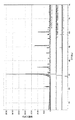
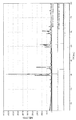
この様にして得られたターゲットは、X線回折測定の結果、In2O3及びGd2Sn2O7、GdInO3を主成分とする酸化物からなることが確認された。図1−10に、それぞれ実施例1−10で作製したターゲットのX線チャートを示す。
表2に、X線回折、ターゲットのICP分析の結果、EPMA(Electron Probe Micro Analyzer)による焼結体の面内の元素分布測定により、In、Gdの分散状態を確認した結果、密度及びバルク抵抗を示す。
As a result of X-ray diffraction measurement, it was confirmed that the target thus obtained was composed of an oxide containing In 2 O 3, Gd 2 Sn 2 O 7 , and GdInO 3 as main components. FIG. 1-10 shows X-ray charts of the targets manufactured in Example 1-10, respectively.
Table 2 shows the results of X-ray diffraction, ICP analysis of the target, and the in-plane element distribution measurement by EPMA (Electron Probe Micro Analyzer) to confirm the dispersion state of In and Gd, and the density and bulk resistance. Indicates.
比較例1
酸化インジウム400gと酸化ガドリニウム600gとを混合させて、ドライビーズミルにて約5時間粉砕・混合した。
次いで、上記で得られた粉末を10mmφの金型に挿入し、金型プレス成形機により100kg/cm2の圧力で予備成形を行った。次に、冷間静水圧プレス成形機により4t/cm2の圧力で圧密化した後、1350℃で10時間焼成した。
Comparative Example 1
400 g of indium oxide and 600 g of gadolinium oxide were mixed and pulverized and mixed in a dry bead mill for about 5 hours.
Subsequently, the powder obtained above was inserted into a 10 mmφ mold, and preformed at a pressure of 100 kg / cm 2 with a mold press molding machine. Next, it was consolidated at a pressure of 4 t / cm 2 using a cold isostatic press molding machine, and then fired at 1350 ° C. for 10 hours.
炉から取出した状態の焼結体には、多くのクラックが発生し、また、割れが観測され、ターゲット(研削、研磨、バッキングプレートへの貼り付け)加工が実施できなかった。
この焼結体は、X線回折測定の結果、GdInO3及びGd2O3を主成分とする酸化物からなる焼結体であることが確認された。
ICP分析の結果、原子比[Gd/(Gd+In)]は0.56であった。
EPMAによる焼結体の面内の元素分布測定により、In、Gdの分散状態を確認した結果、その組成は実質的に不均一であった。また、バルク抵抗は2MΩcm以上であり、ほぼ絶縁材料であった。
In the sintered body taken out from the furnace, many cracks were generated and cracks were observed, and the target (grinding, polishing, pasting to backing plate) processing could not be performed.
As a result of X-ray diffraction measurement, this sintered body was confirmed to be a sintered body made of an oxide containing GdInO 3 and Gd 2 O 3 as main components.
As a result of ICP analysis, the atomic ratio [Gd / (Gd + In)] was 0.56.
As a result of confirming the dispersion state of In and Gd by measuring the element distribution in the surface of the sintered body by EPMA, the composition was substantially non-uniform. Further, the bulk resistance was 2 MΩcm or more, which was almost an insulating material.
本発明のターゲットは、液晶表示装置(LCD)用透明導電膜、エレクトロルミネッセンス(EL)表示素子用透明導電膜、太陽電池用透明導電膜等、種々の用途の透明導電膜をスパッタリング法、エレクトロンビーム蒸着法、イオンプレーティング法により得るためのターゲットとして好適である。例えば、有機EL素子の電極や、半透過・半反射LCD用の透明導電膜を得ることができる。 The target of the present invention is a transparent conductive film for various uses such as a transparent conductive film for liquid crystal display devices (LCD), a transparent conductive film for electroluminescence (EL) display elements, and a transparent conductive film for solar cells. It is suitable as a target for obtaining by vapor deposition or ion plating. For example, an electrode of an organic EL element and a transparent conductive film for a semi-transmissive / semi-reflective LCD can be obtained.
Claims (5)
[Sn/(Gd+Sn+In)]>[Gd/(Gd+Sn+In)] The ratio of Sn [Sn / (Gd + Sn + In): atomic ratio] to the total content of In, Sn and Gd and the ratio of Gd [Gd / (Gd + Sn + In): atomic ratio] satisfy the following relational expression: The oxide target used for sputtering, electron beam evaporation, or ion plating according to claim 1 or 2.
[Sn / (Gd + Sn + In)]> [Gd / (Gd + Sn + In)]
The oxide target used for sputtering, electron beam evaporation, and ion plating according to any one of claims 1 to 4, wherein the bulk resistance is 1 Ωcm or less.
Priority Applications (6)
| Application Number | Priority Date | Filing Date | Title |
|---|---|---|---|
| JP2006218034A JP5000231B2 (en) | 2006-08-10 | 2006-08-10 | Gadolinium oxide-containing oxide target |
| PCT/JP2007/065346 WO2008018403A1 (en) | 2006-08-10 | 2007-08-06 | Lanthanoid-containing oxide target |
| US12/376,838 US8038911B2 (en) | 2006-08-10 | 2007-08-06 | Lanthanoid-containing oxide target |
| CN2007800294770A CN101501240B (en) | 2006-08-10 | 2007-08-06 | Oxide target containing lanthanide |
| KR1020097002580A KR20090051170A (en) | 2006-08-10 | 2007-08-06 | Lanthanoid-containing oxide target |
| TW096129735A TWI441933B (en) | 2006-08-10 | 2007-08-10 | Targets containing oxides of lanthanides |
Applications Claiming Priority (1)
| Application Number | Priority Date | Filing Date | Title |
|---|---|---|---|
| JP2006218034A JP5000231B2 (en) | 2006-08-10 | 2006-08-10 | Gadolinium oxide-containing oxide target |
Publications (2)
| Publication Number | Publication Date |
|---|---|
| JP2008038235A JP2008038235A (en) | 2008-02-21 |
| JP5000231B2 true JP5000231B2 (en) | 2012-08-15 |
Family
ID=39173604
Family Applications (1)
| Application Number | Title | Priority Date | Filing Date |
|---|---|---|---|
| JP2006218034A Expired - Fee Related JP5000231B2 (en) | 2006-08-10 | 2006-08-10 | Gadolinium oxide-containing oxide target |
Country Status (1)
| Country | Link |
|---|---|
| JP (1) | JP5000231B2 (en) |
Families Citing this family (2)
| Publication number | Priority date | Publication date | Assignee | Title |
|---|---|---|---|---|
| US8333913B2 (en) * | 2007-03-20 | 2012-12-18 | Idemitsu Kosan Co., Ltd. | Sputtering target, oxide semiconductor film and semiconductor device |
| CN116283271B (en) * | 2023-03-07 | 2024-03-12 | 宁波大学 | Gd with high refractive index and high optical quality 2 Sn 2 O 7 Method for preparing pyrochlore type transparent ceramic |
Family Cites Families (1)
| Publication number | Priority date | Publication date | Assignee | Title |
|---|---|---|---|---|
| JP2004119272A (en) * | 2002-09-27 | 2004-04-15 | Idemitsu Kosan Co Ltd | Organic el device and substrate used for it |
-
2006
- 2006-08-10 JP JP2006218034A patent/JP5000231B2/en not_active Expired - Fee Related
Also Published As
| Publication number | Publication date |
|---|---|
| JP2008038235A (en) | 2008-02-21 |
Similar Documents
| Publication | Publication Date | Title |
|---|---|---|
| TWI441933B (en) | Targets containing oxides of lanthanides | |
| EP1408137B1 (en) | Sputtering target for the deposition of a transparent conductive film | |
| JP4850378B2 (en) | Sputtering target, transparent conductive oxide, and method for producing sputtering target | |
| EP2463256B1 (en) | Oxide sinter, method for producing same, target and transparent conductive film | |
| JP5109418B2 (en) | ZnO vapor deposition material, method for producing the same, and method for forming ZnO film | |
| TWI394852B (en) | A sputtering target, a method for manufacturing the same, and a transparent conductive film | |
| JP4926977B2 (en) | Gallium oxide-zinc oxide sintered sputtering target | |
| JP4054054B2 (en) | Gallium oxide-zinc oxide sputtering target, method for forming transparent conductive film, and transparent conductive film | |
| TWI761664B (en) | Oxide sputtering target, manufacturing method thereof, and oxide thin film formed using the oxide sputtering target | |
| CN103717779A (en) | Zn-sn-o type oxide sintered body and method for producing same | |
| KR101294986B1 (en) | In Sm OXIDE SPUTTERING TARGET | |
| JPWO2007000878A1 (en) | Gallium oxide-zinc oxide sputtering target, method for forming transparent conductive film, and transparent conductive film | |
| JPWO2011115177A1 (en) | Transparent conductive film | |
| JP5000230B2 (en) | Lanthanum oxide containing oxide target | |
| WO2011052375A1 (en) | Indium oxide sintered body and indium oxide transparent conductive film | |
| JP4960052B2 (en) | Ytterbium oxide containing oxide target | |
| JP5000231B2 (en) | Gadolinium oxide-containing oxide target | |
| JP5018553B2 (en) | ZnO vapor deposition material, method for producing the same, and ZnO film formed thereby | |
| JP5063968B2 (en) | Erbium oxide-containing oxide target | |
| JP4960041B2 (en) | Neodymium oxide-containing oxide target | |
| JP4960053B2 (en) | Oxide target containing dysprosium oxide | |
| JP2012148937A (en) | Electrically conductive composite oxide, zinc oxide type sintered body, method for manufacturing it and target | |
| JP2008255472A (en) | ZnO VAPOR DEPOSITION MATERIAL AND ZnO FILM FORMED THEREFROM | |
| WO2015052927A1 (en) | Sputtering target and method for producing same | |
| KR20150039753A (en) | Oxide Sintered Body and Tablet Obtained by Processing Same |
Legal Events
| Date | Code | Title | Description |
|---|---|---|---|
| A621 | Written request for application examination |
Free format text: JAPANESE INTERMEDIATE CODE: A621 Effective date: 20090217 |
|
| A131 | Notification of reasons for refusal |
Free format text: JAPANESE INTERMEDIATE CODE: A131 Effective date: 20111206 |
|
| A521 | Written amendment |
Free format text: JAPANESE INTERMEDIATE CODE: A523 Effective date: 20120130 |
|
| A131 | Notification of reasons for refusal |
Free format text: JAPANESE INTERMEDIATE CODE: A131 Effective date: 20120221 |
|
| A521 | Written amendment |
Free format text: JAPANESE INTERMEDIATE CODE: A523 Effective date: 20120327 |
|
| TRDD | Decision of grant or rejection written | ||
| A01 | Written decision to grant a patent or to grant a registration (utility model) |
Free format text: JAPANESE INTERMEDIATE CODE: A01 Effective date: 20120417 |
|
| A01 | Written decision to grant a patent or to grant a registration (utility model) |
Free format text: JAPANESE INTERMEDIATE CODE: A01 |
|
| A61 | First payment of annual fees (during grant procedure) |
Free format text: JAPANESE INTERMEDIATE CODE: A61 Effective date: 20120516 |
|
| R150 | Certificate of patent or registration of utility model |
Ref document number: 5000231 Country of ref document: JP Free format text: JAPANESE INTERMEDIATE CODE: R150 Free format text: JAPANESE INTERMEDIATE CODE: R150 |
|
| FPAY | Renewal fee payment (event date is renewal date of database) |
Free format text: PAYMENT UNTIL: 20150525 Year of fee payment: 3 |
|
| LAPS | Cancellation because of no payment of annual fees |