JP4987966B2 - Radiation generating device, lithographic apparatus, device manufacturing method and device manufactured thereby - Google Patents
Radiation generating device, lithographic apparatus, device manufacturing method and device manufactured thereby Download PDFInfo
- Publication number
- JP4987966B2 JP4987966B2 JP2009509462A JP2009509462A JP4987966B2 JP 4987966 B2 JP4987966 B2 JP 4987966B2 JP 2009509462 A JP2009509462 A JP 2009509462A JP 2009509462 A JP2009509462 A JP 2009509462A JP 4987966 B2 JP4987966 B2 JP 4987966B2
- Authority
- JP
- Japan
- Prior art keywords
- electrode
- supply line
- terminal
- high inductance
- inductance unit
- Prior art date
- Legal status (The legal status is an assumption and is not a legal conclusion. Google has not performed a legal analysis and makes no representation as to the accuracy of the status listed.)
- Expired - Fee Related
Links
Images


Classifications
-
- H—ELECTRICITY
- H05—ELECTRIC TECHNIQUES NOT OTHERWISE PROVIDED FOR
- H05G—X-RAY TECHNIQUE
- H05G2/00—Apparatus or processes specially adapted for producing X-rays, not involving X-ray tubes, e.g. involving generation of a plasma
- H05G2/001—X-ray radiation generated from plasma
- H05G2/003—X-ray radiation generated from plasma being produced from a liquid or gas
-
- B—PERFORMING OPERATIONS; TRANSPORTING
- B82—NANOTECHNOLOGY
- B82Y—SPECIFIC USES OR APPLICATIONS OF NANOSTRUCTURES; MEASUREMENT OR ANALYSIS OF NANOSTRUCTURES; MANUFACTURE OR TREATMENT OF NANOSTRUCTURES
- B82Y10/00—Nanotechnology for information processing, storage or transmission, e.g. quantum computing or single electron logic
-
- G—PHYSICS
- G03—PHOTOGRAPHY; CINEMATOGRAPHY; ANALOGOUS TECHNIQUES USING WAVES OTHER THAN OPTICAL WAVES; ELECTROGRAPHY; HOLOGRAPHY
- G03F—PHOTOMECHANICAL PRODUCTION OF TEXTURED OR PATTERNED SURFACES, e.g. FOR PRINTING, FOR PROCESSING OF SEMICONDUCTOR DEVICES; MATERIALS THEREFOR; ORIGINALS THEREFOR; APPARATUS SPECIALLY ADAPTED THEREFOR
- G03F7/00—Photomechanical, e.g. photolithographic, production of textured or patterned surfaces, e.g. printing surfaces; Materials therefor, e.g. comprising photoresists; Apparatus specially adapted therefor
- G03F7/70—Microphotolithographic exposure; Apparatus therefor
- G03F7/70008—Production of exposure light, i.e. light sources
- G03F7/70016—Production of exposure light, i.e. light sources by discharge lamps
-
- G—PHYSICS
- G03—PHOTOGRAPHY; CINEMATOGRAPHY; ANALOGOUS TECHNIQUES USING WAVES OTHER THAN OPTICAL WAVES; ELECTROGRAPHY; HOLOGRAPHY
- G03F—PHOTOMECHANICAL PRODUCTION OF TEXTURED OR PATTERNED SURFACES, e.g. FOR PRINTING, FOR PROCESSING OF SEMICONDUCTOR DEVICES; MATERIALS THEREFOR; ORIGINALS THEREFOR; APPARATUS SPECIALLY ADAPTED THEREFOR
- G03F7/00—Photomechanical, e.g. photolithographic, production of textured or patterned surfaces, e.g. printing surfaces; Materials therefor, e.g. comprising photoresists; Apparatus specially adapted therefor
- G03F7/70—Microphotolithographic exposure; Apparatus therefor
- G03F7/70008—Production of exposure light, i.e. light sources
- G03F7/70033—Production of exposure light, i.e. light sources by plasma extreme ultraviolet [EUV] sources
-
- H—ELECTRICITY
- H05—ELECTRIC TECHNIQUES NOT OTHERWISE PROVIDED FOR
- H05G—X-RAY TECHNIQUE
- H05G2/00—Apparatus or processes specially adapted for producing X-rays, not involving X-ray tubes, e.g. involving generation of a plasma
- H05G2/001—X-ray radiation generated from plasma
- H05G2/003—X-ray radiation generated from plasma being produced from a liquid or gas
- H05G2/005—X-ray radiation generated from plasma being produced from a liquid or gas containing a metal as principal radiation generating component
Abstract
Description
本発明は、放射生成デバイス、リソグラフィ装置、デバイス製造方法、およびそれによって製造したデバイスに関する。 The present invention relates to a radiation generating device, a lithographic apparatus, a device manufacturing method, and a device manufactured thereby.
リソグラフィ装置は、所望のパターンを基板上、通常、基板のターゲット部分上に付与する機械である。リソグラフィ装置は、例えば、集積回路(IC)の製造に用いることができる。その場合、ICの個々の層上に形成される回路パターンを生成するために、マスクまたはレチクルとも呼ばれるパターニングデバイスを用いることができる。このパターンは、基板(例えば、シリコンウェーハ)上のターゲット部分(例えば、ダイの一部、または1つ以上のダイを含む)に転写することができる。通常、パターンの転写は、基板上に設けられた放射感応性材料(レジスト)層上への結像によって行われる。一般には、単一の基板が、連続的にパターニングされる隣接したターゲット部分のネットワークを含んでいる。公知のリソグラフィ装置としては、ターゲット部分上にパターン全体を一度に露光することにより各ターゲット部分を照射する、いわゆるステッパ、および放射ビームによってある特定の方向(「スキャン」方向)にパターンをスキャンすると同時に、この方向に平行または逆平行に基板をスキャンすることにより各ターゲット部分を照射する、いわゆるスキャナが含まれる。パターンを基板上にインプリントすることにより、パターニングデバイスから基板にパターンを転写することも可能である。 A lithographic apparatus is a machine that applies a desired pattern onto a substrate, usually onto a target portion of the substrate. A lithographic apparatus can be used, for example, in the manufacture of integrated circuits (ICs). In that case, a patterning device, also referred to as a mask or a reticle, may be used to generate a circuit pattern formed on an individual layer of the IC. This pattern can be transferred onto a target portion (eg including part of, one, or more dies) on a substrate (eg a silicon wafer). Usually, the pattern is transferred by imaging on a radiation-sensitive material (resist) layer provided on the substrate. In general, a single substrate will contain a network of adjacent target portions that are successively patterned. Known lithographic apparatus include a so-called stepper that irradiates each target portion by exposing the entire pattern onto the target portion at once, and simultaneously scanning the pattern in a certain direction ("scan" direction) with a radiation beam. Also included are so-called scanners that irradiate each target portion by scanning the substrate parallel or antiparallel to this direction. It is also possible to transfer the pattern from the patterning device to the substrate by imprinting the pattern onto the substrate.
リソグラフィ装置において、基板上に結像できるフィーチャのサイズは、放射ビームの波長によって制限される。より高い濃度のデバイス、よってより速い操作スピードの集積回路を生産するためには、より小さいフィーチャを結像することが望ましい。ほとんどの現在のリソグラフィ投影装置は、水銀ランプまたはエキシマレーザによって生成される紫外線を用いるが、より短い波長の放射(例えば約13nm)を使用することが提案されている。このような放射は、極紫外線(EUV)または軟X線と呼ばれ、可能な放射源には、レーザ生成プラズマ源および放電プラズマ源が含まれる。これらのプラズマ源は高電圧を使用し、操作中の安全性の問題に関するオペレータの認識を必要とする。 In a lithographic apparatus, the size of features that can be imaged on a substrate is limited by the wavelength of the radiation beam. It is desirable to image smaller features in order to produce higher density devices, and thus faster operating speed integrated circuits. Most current lithographic projection apparatus use ultraviolet light generated by mercury lamps or excimer lasers, but it has been proposed to use shorter wavelength radiation (eg, about 13 nm). Such radiation is called extreme ultraviolet (EUV) or soft x-ray, and possible sources include laser-produced plasma sources and discharge plasma sources. These plasma sources use high voltages and require operator awareness of safety issues during operation.
従来技術に鑑みて性能が向上した放射生成装置を提供することが望ましい。 It is desirable to provide a radiation generating device with improved performance in view of the prior art.
その目的を達成するために、一実施形態において、本発明は、電動放電により放射を生成する装置を提供する。当該装置は、第1電極および第2電極であって、前記第1および第2電極の間にガス媒体におけるプラズマ点火を可能とする距離をおいて構成された第1電極および第2電極、および、前記第1電極への第1端子および前記第2電極への第2端子と電気的に接続されるコンデンサバンクであって、前記プラズマ点火に必要とされる放電エネルギーを蓄積するように構成されたコンデンサバンクを含み、前記第1電極、前記第2電極、および前記コンデンサバンクは電気回路を形成し、少なくとも前記第1電極は、第1供給ラインを介して供給される導電流体によって形成される。 To achieve that objective, in one embodiment, the present invention provides an apparatus for generating radiation by electric discharge. The apparatus includes a first electrode and a second electrode, the first electrode and the second electrode being configured with a distance between the first electrode and the second electrode that enables plasma ignition in a gas medium, and A capacitor bank electrically connected to the first terminal to the first electrode and the second terminal to the second electrode, wherein the capacitor bank is configured to accumulate discharge energy required for the plasma ignition. The first electrode, the second electrode, and the capacitor bank form an electric circuit, and at least the first electrode is formed by a conductive fluid supplied through a first supply line. .
上記装置は、前記第1端子および前記第2端子の少なくとも1つに接続されて、時変的に前記コンデンサバンクに帯電させるためのチャージャ、および、前記第1供給ラインにおける前記第1端子の上流に、前記電気回路を電気的に分離するように設けられた第1高インダクタンスユニット、をさらに含み得る。 The apparatus includes a charger connected to at least one of the first terminal and the second terminal for charging the capacitor bank in a time-varying manner, and upstream of the first terminal in the first supply line. And a first high inductance unit provided to electrically isolate the electrical circuit.
さらに、本発明は、放射ビームを調整するように構成された照明システム、パターニングデバイスを支持するように構成されたサポートであって、前記パターニングデバイスが、前記放射ビームの断面にパターンを付与して、パターン付き放射ビームを形成するように構成されているサポート、基板を保持するように構成された基板テーブル、および、前記基板のターゲット部分に前記パターン付き放射ビームを投影するように構成された投影システムを含み、前記照明システムは、電動放電により放射を生成する装置を含む、リソグラフィ装置を提供する。 The present invention further includes an illumination system configured to condition a radiation beam, a support configured to support a patterning device, wherein the patterning device imparts a pattern to a cross-section of the radiation beam. A support configured to form a patterned radiation beam, a substrate table configured to hold a substrate, and a projection configured to project the patterned radiation beam onto a target portion of the substrate The illumination system includes a system, wherein the illumination system includes an apparatus that generates radiation by an electric discharge.
さらに、本発明はそのようなリソグラフィ装置により製造されたデバイスを提供する。 Furthermore, the present invention provides a device manufactured by such a lithographic apparatus.
また、本発明は、電動放電により放射を生成する装置に関する。当該装置は、第1電極および第2電極であって、前記第1および第2電極の間にガス媒体におけるプラズマ点火を可能とする距離をおいて構成された第1電極および第2電極、および前記第1電極への第1端子および前記第2電極への第2端子と電気的に接続されるコンデンサバンクであって、前記プラズマ点火に必要とされる放電エネルギーを蓄積するように構成されたコンデンサバンクを含み、前記第1電極、前記第2電極、および前記コンデンサバンクは電気回路を形成し、前記第1電極は、第1供給ラインを介して供給される導電流体によって形成され、前記第2電極は、第2供給ラインを介して供給される導電流体によって形成され、前記第1供給ラインは、特定の材料が第1ジェットの形状をとる前記第1電極を提供するように構成される第1ノズルを含み、前記第2供給ラインは、特定の材料が第2ジェットの形状をとる前記第2電極を提供するように構成される第2ノズルを含む。 The invention also relates to an apparatus for generating radiation by electric discharge. The apparatus includes a first electrode and a second electrode, the first electrode and the second electrode being configured with a distance between the first electrode and the second electrode that enables plasma ignition in a gas medium, and A capacitor bank electrically connected to a first terminal to the first electrode and a second terminal to the second electrode, configured to store discharge energy required for the plasma ignition A capacitor bank, wherein the first electrode, the second electrode, and the capacitor bank form an electric circuit, the first electrode is formed by a conductive fluid supplied through a first supply line, and The two electrodes are formed by a conductive fluid supplied through a second supply line, the first supply line providing the first electrode in which a specific material takes the form of a first jet. Includes a first nozzle which is made, the second supply line includes a second nozzle configured to provide the second electrode a particular material takes the shape of the second jet.
上記装置は、時変的に前記コンデンサバンクに帯電させるためのチャージャ、前記第1供給ラインにおける前記第1端子の上流に設けられた第1高インダクタンスユニットであって、前記第1供給ラインの第1コイル状部分を含む、第1高インダクタンスユニット、および、前記第2供給ラインにおける前記第2端子の上流に設けられた第2高インダクタンスユニットであって、前記第2供給ラインの第2コイル状部分を含む、第2高インダクタンスユニット、をさらに含み得る。 The apparatus includes a charger for charging the capacitor bank in a time-varying manner, a first high-inductance unit provided upstream of the first terminal in the first supply line, A first high-inductance unit including one coil-shaped portion; and a second high-inductance unit provided upstream of the second terminal in the second supply line, wherein the second coil shape of the second supply line A second high inductance unit including a portion may be further included.
本発明のいくつかの実施形態を、単なる例として、添付の概略図を参照して以下に説明する。これらの図面において同じ参照符号は対応する部分を示す。 Several embodiments of the present invention are described below by way of example only and with reference to the accompanying schematic drawings. In these drawings, the same reference numerals indicate corresponding parts.
図1は、本発明の一実施形態に係るリソグラフィ装置を概略的に示している。このリソグラフィ装置は、放射ビームB(例えば、紫外線またはEUV放射)を調整するように構成された照明システム(イルミネータ)ILを含む。サポート(例えば、マスクテーブル)MTは、パターニングデバイス(例えば、マスク)MAを支持するように構成され、かつ特定のパラメータに従ってパターニングデバイスを正確に位置付けるように構成された第1ポジショナPMに連結されている。基板テーブル(例えば、ウェーハテーブル)WTは、基板(例えば、レジストコートウェーハ)Wを保持するように構成され、かつ特定のパラメータに従って基板を正確に位置付けるように構成された第2ポジショナPWに連結されている。投影システム(例えば、屈折投影レンズシステム)PSは、パターニングデバイスMAによって放射ビームBに付けられたパターンを基板Wのターゲット部分C(例えば、1つ以上のダイを含む)上に投影するように構成されている。 FIG. 1 schematically depicts a lithographic apparatus according to one embodiment of the invention. The lithographic apparatus includes an illumination system (illuminator) IL configured to condition a radiation beam B (eg, ultraviolet or EUV radiation). A support (eg, mask table) MT is coupled to a first positioner PM configured to support the patterning device (eg, mask) MA and configured to accurately position the patterning device according to certain parameters. Yes. The substrate table (eg, wafer table) WT is coupled to a second positioner PW that is configured to hold the substrate (eg, resist coated wafer) W and is configured to accurately position the substrate according to certain parameters. ing. Projection system (eg, refractive projection lens system) PS is configured to project a pattern imparted to radiation beam B by patterning device MA onto target portion C (eg, including one or more dies) of substrate W. Has been.
照明システムとしては、放射を誘導し、整形し、および/または制御するために、屈折型、反射型、磁気型、電磁型、静電型、またはその他のタイプの光コンポーネント、あるいはそれらのあらゆる組合せなどの様々なタイプの光コンポーネントを含むことができる。 Illumination systems include refractive, reflective, magnetic, electromagnetic, electrostatic, or other types of optical components, or any combination thereof, to induce, shape, and / or control radiation Various types of optical components can be included.
サポートは、パターニングデバイスの重量を支えるなどしてパターニングデバイスを支持する。サポートは、パターニングデバイスの配向、リソグラフィ装置の設計、および、パターニングデバイスが真空環境内で保持されているか否かなどの他の条件に応じた態様で、パターニングデバイスを保持する。サポートは、機械式、真空式、静電式またはその他のクランプ技術を使って、パターニングデバイスを保持することができる。サポートは、例えば、必要に応じて固定または可動式にすることができるフレームまたはテーブルであってもよい。サポートは、パターニングデバイスを、例えば、投影システムに対して所望の位置に確実に置くことができる。本明細書において使用される「レチクル」または「マスク」という用語はすべて、より一般的な「パターニングデバイス」という用語と同義であると考えるとよい。 The support supports the patterning device, such as by supporting the weight of the patterning device. The support holds the patterning device in a manner that depends on the orientation of the patterning device, the design of the lithographic apparatus, and other conditions, such as whether or not the patterning device is held in a vacuum environment. The support can hold the patterning device using mechanical, vacuum, electrostatic or other clamping techniques. The support may be, for example, a frame or table that can be fixed or movable as required. The support may ensure that the patterning device is at a desired position, for example with respect to the projection system. Any use of the terms “reticle” or “mask” herein may be considered synonymous with the more general term “patterning device.”
本明細書において使用される「パターニングデバイス」という用語は、基板のターゲット部分内にパターンを作り出すように、放射ビームの断面にパターンを与えるために使用できるあらゆるデバイスを指していると、広く解釈されるべきである。なお、留意すべき点として、放射ビームに付与されたパターンは、例えば、そのパターンが位相シフトフィーチャまたはいわゆるアシストフィーチャを含む場合、基板のターゲット部分内の所望のパターンに正確に一致しない場合もある。通常、放射ビームに付けたパターンは、集積回路などのターゲット部分内に作り出されるデバイス内の特定機能層に対応することになる。 As used herein, the term “patterning device” is broadly interpreted to refer to any device that can be used to provide a pattern in a cross-section of a radiation beam so as to create a pattern in a target portion of a substrate. Should be. It should be noted that the pattern imparted to the radiation beam may not exactly match the desired pattern in the target portion of the substrate, for example if the pattern includes phase shift features or so-called assist features. . Typically, the pattern applied to the radiation beam will correspond to a particular functional layer in a device being created in the target portion, such as an integrated circuit.
パターニングデバイスは、透過型であっても、反射型であってもよい。パターニングデバイスの例としては、マスク、プログラマブルミラーアレイ、およびプログラマブルLCDパネルが含まれる。マスクは、リソグラフィでは公知であり、バイナリ、レゼンソン型(alternating)位相シフト、およびハーフトーン型(attenuated)位相シフトなどのマスク型、ならびに種々のハイブリッドマスク型を含む。プログラマブルミラーアレイの一例では、小型ミラーのマトリックス配列が用いられており、各小型ミラーは、入射する放射ビームを様々な方向に反射させるように、個別に傾斜させることができる。傾斜されたミラーは、ミラーマトリックスによって反射される放射ビームにパターンを付ける。 The patterning device may be transmissive or reflective. Examples of patterning devices include masks, programmable mirror arrays, and programmable LCD panels. Masks are well known in lithography and include mask types such as binary, alternating phase shift, and attenuated phase shift, as well as various hybrid mask types. One example of a programmable mirror array uses a matrix array of small mirrors, and each small mirror can be individually tilted to reflect the incoming radiation beam in various directions. The tilted mirror patterns the radiation beam reflected by the mirror matrix.
本明細書において使用される「投影システム」という用語は、使われている露光放射にとって、あるいは液浸液の使用または真空の使用といった他の要因にとって適切な、屈折型、反射型、反射屈折型、磁気型、電磁型、および静電型光学系、またはそれらのあらゆる組合せを含むあらゆる型の投影システムを包含していると広く解釈されるべきである。本明細書において使用される「投影レンズ」という用語はすべて、より一般的な「投影システム」という用語と同義であると考えるとよい。 As used herein, the term “projection system” refers to refractive, reflective, and catadioptric types that are appropriate for the exposure radiation used or for other factors such as the use of immersion liquid or the use of vacuum. It should be construed broadly to encompass any type of projection system, including magnetic, electromagnetic, and electrostatic optics, or any combination thereof. Any use of the term “projection lens” herein may be considered as synonymous with the more general term “projection system”.
本明細書に示されているとおり、リソグラフィ装置は、反射型のもの(例えば、反射型マスクを採用しているもの)である。あるいは、リソグラフィ装置は、透過型のもの(例えば、透過型マスクを採用しているもの)でもよい。 As shown herein, the lithographic apparatus is of a reflective type (eg employing a reflective mask). Alternatively, the lithographic apparatus may be of a transmissive type (eg employing a transmissive mask).
リソグラフィ装置は、2つ(デュアルステージ)以上の基板テーブル(および/または2つ以上のマスクテーブル)を有する型のものであってもよい。そのような「マルチステージ」機械においては、追加のテーブルは並行して使うことができ、または予備工程を1つ以上のテーブル上で実行しつつ、別の1つ以上のテーブルを露光用に使うこともできる。 The lithographic apparatus may be of a type having two (dual stage) or more substrate tables (and / or two or more mask tables). In such “multi-stage” machines, additional tables can be used in parallel, or one or more tables are used for exposure while a preliminary process is performed on one or more tables. You can also
また、リソグラフィ装置は、投影システムと基板との間の空間を満たすように、比較的高屈折率を有する液体(例えば、水)によって基板の少なくとも一部を覆うことができるタイプのものであってもよい。また、リソグラフィ装置内の別の空間(例えば、マスクと投影システムとの間)に液浸液を加えてもよい。液浸技術は、投影システムの開口数を増加させるための技術においてよく知られている。本明細書において使用される「液浸」という用語は、基板のような構造物を液体内に沈めなければならないという意味ではなく、単に、露光中、投影システムと基板との間に液体があるということを意味するものである。 The lithographic apparatus may also be of a type capable of covering at least a portion of the substrate with a liquid having a relatively high refractive index (eg, water) so as to fill a space between the projection system and the substrate. Also good. An immersion liquid may also be added to another space in the lithographic apparatus (eg, between the mask and the projection system). Immersion techniques are well known in the art for increasing the numerical aperture of projection systems. The term “immersion” as used herein does not mean that a structure, such as a substrate, must be submerged in the liquid, but simply the liquid between the projection system and the substrate during exposure. It means that.
図1を参照すると、イルミネータILは、放射源SOから放射を受ける。例えば、放射源がエキシマレーザである場合、放射源とリソグラフィ装置は、別個の構成要素であってもよい。そのような場合には、放射源は、リソグラフィ装置の一部を形成しているとはみなされず、また放射ビームは、放射源SOからイルミネータILへ、例えば、適切な誘導ミラーおよび/またはビームエキスパンダを含むビームデリバリシステムBDを使って送られる。その他の場合においては、例えば、放射源が水銀ランプである場合、放射源は、リソグラフィ装置の一体部分とすることもできる。放射源SOおよびイルミネータILは、必要ならばビームデリバリシステムBDとともに、放射システムと呼んでもよい。 Referring to FIG. 1, the illuminator IL receives radiation from a radiation source SO. For example, if the radiation source is an excimer laser, the radiation source and the lithographic apparatus may be separate components. In such a case, the radiation source is not considered to form part of the lithographic apparatus, and the radiation beam is directed from the radiation source SO to the illuminator IL, eg, a suitable guiding mirror and / or beam extractor. Sent using a beam delivery system BD that includes a panda. In other cases the source may be an integral part of the lithographic apparatus, for example when the source is a mercury lamp. The radiation source SO and the illuminator IL may be referred to as a radiation system, together with a beam delivery system BD if necessary.
イルミネータILは、放射ビームの角度強度分布を調節するアジャスタADを含むことができる。一般に、イルミネータの瞳面内の強度分布の少なくとも外側および/または内側半径範囲(通常、それぞれσ−outerおよびσ−innerと呼ばれる)を調節することができる。さらに、イルミネータILは、インテグレータINおよびコンデンサCOといった様々な他のコンポーネントを含むことができる。イルミネータを使って放射ビームを調整すれば、放射ビームの断面に所望の均一性および強度分布をもたせることができる。 The illuminator IL may include an adjuster AD that adjusts the angular intensity distribution of the radiation beam. In general, at least the outer and / or inner radial extent (commonly referred to as σ-outer and σ-inner, respectively) of the intensity distribution in the illuminator pupil plane can be adjusted. In addition, the illuminator IL may include various other components such as an integrator IN and a capacitor CO. By adjusting the radiation beam using an illuminator, the desired uniformity and intensity distribution can be provided in the cross section of the radiation beam.
放射ビームBは、サポート(例えば、マスクテーブルMT)上に保持されているパターニングデバイス(例えば、マスクMA)上に入射して、パターニングデバイスによってパターン形成される。マスクMAを通り抜けた後、放射ビームBは投影システムPSを通過し、投影システムPSは、基板Wのターゲット部分C上にビームの焦点をあわせる。第2ポジショナPWおよび位置センサIF2(例えば、干渉計デバイス、リニアエンコーダ、または静電容量センサ)を使って、例えば、様々なターゲット部分Cを放射ビームBの経路内に位置付けるように、基板テーブルWTを正確に動かすことができる。同様に、第1ポジショナPMおよび別の位置センサIF1を使い、例えば、マスクライブラリからマスクを機械的に取り出した後またはスキャン中に、マスクMAを放射ビームBの経路に対して正確に位置付けることもできる。通常、マスクテーブルMTの移動は、第1ポジショナPMの一部を形成するロングストロークモジュール(粗動位置決め)およびショートストロークモジュール(微動位置決め)を使って達成することができる。同様に、基板テーブルWTの移動も、第2ポジショナPWの一部を形成するロングストロークモジュールおよびショートストロークモジュールを使って達成することができる。ステッパの場合は(スキャナとは対照的に)、マスクテーブルMTは、ショートストロークアクチュエータのみに連結されてもよく、または固定されてもよい。マスクMAおよび基板Wは、マスクアライメントマークM1およびM2と、基板アライメントマークP1およびP2とを使って、位置合わせされてもよい。例示では基板アライメントマークが専用ターゲット部分を占めているが、基板アライメントマークをターゲット部分とターゲット部分との間の空間内に置くこともできる(これらは、スクライブラインアライメントマークとして公知である)。同様に、複数のダイがマスクMA上に設けられている場合、マスクアライメントマークは、ダイとダイの間に置かれてもよい。 The radiation beam B is incident on the patterning device (eg, mask MA), which is held on the support (eg, mask table MT), and is patterned by the patterning device. After passing through the mask MA, the radiation beam B passes through the projection system PS, which focuses the beam on the target portion C of the substrate W. Using the second positioner PW and the position sensor IF2 (eg interferometer device, linear encoder, or capacitive sensor), for example, the substrate table WT so as to position the various target portions C in the path of the radiation beam B. Can be moved accurately. Similarly, the first positioner PM and another position sensor IF1 may be used to accurately position the mask MA with respect to the path of the radiation beam B, eg after mechanical removal of the mask from the mask library or during a scan. it can. In general, the movement of the mask table MT can be achieved by using a long stroke module (coarse positioning) and a short stroke module (fine positioning) that form part of the first positioner PM. Similarly, movement of the substrate table WT can also be achieved using a long stroke module and a short stroke module that form part of the second positioner PW. In the case of a stepper (as opposed to a scanner) the mask table MT may be connected to a short stroke actuator only, or may be fixed. Mask MA and substrate W may be aligned using mask alignment marks M1 and M2 and substrate alignment marks P1 and P2. In the example, the substrate alignment mark occupies the dedicated target portion, but the substrate alignment mark can also be placed in the space between the target portion (these are known as scribe line alignment marks). Similarly, if a plurality of dies are provided on the mask MA, the mask alignment mark may be placed between the dies.
例示の装置は、以下に説明するモードのうち少なくとも1つのモードで使用できる。 The example apparatus can be used in at least one of the modes described below.
1.ステップモードにおいては、マスクテーブルMTおよび基板テーブルWTを基本的に静止状態に保ちつつ、放射ビームに付けられたパターン全体を一度に(すなわち、単一静止露光)ターゲット部分C上に投影する。その後、基板テーブルWTは、Xおよび/またはY方向に移動され、それによって別のターゲット部分Cを露光することができる。ステップモードにおいては、露光フィールドの最大サイズによって、単一静止露光時に結像されるターゲット部分Cのサイズが限定される。 1. In step mode, the entire pattern applied to the radiation beam is projected onto the target portion C at once (ie, a single static exposure) while the mask table MT and substrate table WT remain essentially stationary. Thereafter, the substrate table WT is moved in the X and / or Y direction so that another target portion C can be exposed. In step mode, the maximum size of the exposure field limits the size of the target portion C imaged during a single static exposure.
2.スキャンモードにおいては、マスクテーブルMTおよび基板テーブルWTを同期的にスキャンする一方で、放射ビームに付けられたパターンをターゲット部分C上に投影する(すなわち、単一動的露光)。マスクテーブルMTに対する基板テーブルWTの速度および方向は、投影システムPSの(縮小)拡大率および像反転特性によって決めることができる。スキャンモードにおいては、露光フィールドの最大サイズよって、単一動的露光時のターゲット部分の幅(非スキャン方向)が限定される一方、スキャン動作の長さによって、ターゲット部分の高さ(スキャン方向)が決まる。 2. In scan mode, the mask table MT and substrate table WT are scanned synchronously while a pattern imparted to the radiation beam is projected onto a target portion C (ie, a single dynamic exposure). The speed and direction of the substrate table WT relative to the mask table MT can be determined by the (reduction) magnification factor and image reversal characteristics of the projection system PS. In the scan mode, the maximum size of the exposure field limits the width of the target portion during single dynamic exposure (non-scan direction), while the length of the scan operation determines the height of the target portion (scan direction). Determined.
3.別のモードにおいては、プログラマブルパターニングデバイスを保持した状態で、マスクテーブルMTを基本的に静止状態に保ち、また基板テーブルWTを動かす、またはスキャンする一方で、放射ビームに付けられているパターンをターゲット部分C上に投影する。このモードにおいては、通常、パルス放射源が採用されており、さらにプログラマブルパターニングデバイスは、基板テーブルWTの移動後ごとに、またはスキャン中の連続する放射パルスと放射パルスとの間に、必要に応じて更新される。この動作モードは、前述の型のプログラマブルミラーアレイといったプログラマブルパターニングデバイスを利用するマスクレスリソグラフィに容易に適用することができる。 3. In another mode, while holding the programmable patterning device, the mask table MT remains essentially stationary and the substrate table WT is moved or scanned while the pattern attached to the radiation beam is targeted. Project onto part C. In this mode, a pulsed radiation source is typically employed, and the programmable patterning device can also be used after each movement of the substrate table WT or between successive radiation pulses during a scan as needed. Updated. This mode of operation can be readily applied to maskless lithography that utilizes programmable patterning device, such as a programmable mirror array of a type as described above.
上述の使用モードの組合せおよび/またはバリエーション、あるいは完全に異なる使用モードもまた採用可能である。 Combinations and / or variations on the above described modes of use or entirely different modes of use may also be employed.
この説明において、本発明の一実施形態を、本出願人による米国特許出願第2006−0011864号に記載の放射源に適用される単なる例として、以下に説明する。しかし、類似のまたはその他の実施形態を、異なる放射源、例えば、Philipsによる国際公開公報WO2005/025280号に記載のEUV/軟X線源に適用し得ることが理解されるべきである。 In this description, one embodiment of the present invention is described below as merely an example applied to the radiation source described in commonly assigned US Patent Application No. 2006-0011864. However, it should be understood that similar or other embodiments may be applied to different radiation sources, such as the EUV / soft X-ray source described in Philips International Publication No. WO 2005/025280.
図2は、米国特許出願第2006−0011864号で知られている放射源SO’を示す。放射源SO’は、放電エネルギーを蓄積するように構成されたコンデンサバンク24(この場合は1つのコンデンサを含む)に電気的に接続される2つのノズル21a、21bを収容するように構成されたハウジング20を含む。コンデンサバンク24は、正端子Bおよび負端子Aを有する。ノズル21a、21bは液体の導電ジェット(electrically conductive jets)23a、23bを提供する。液体は、液体流を収容するように構成された供給ライン(図示なし)、例えば、適切なホース又はパイプを介して供給される。本説明中、液体は、液体状態の材料(例えば、溶解物)およびキャリアとしての液体に浸漬された固形粒子の両方を意味する。液体は、スズ(Sn)、インジウム(In)、ガリウム(Ga)、およびリチウム(Li)を含む群から選択される1つ以上の元素を含み得る。Sn、In、Ga、またはLiといった導電材料を使用することにより、ジェット23a、23bはコンデンサバンク24と電気的に接続される。従って、ジェット23a、23bは電極であると考えられ得る。図2に示された場合において、ジェット23aにはプラスの電圧が提供され、従って、陽極として機能する。他方のジェット、すなわち、ジェット23bにはマイナスの電圧が提供されて陰極として機能する。
FIG. 2 shows a radiation source SO 'known from US patent application 2006-0011864. The radiation source SO ′ is configured to accommodate two
ハウジング20は、さらに2つのリザーバ25a、25bを収容する。ジェット23a、23bは、ハウジング20内の空間に進むと、小滴26a、26bにそれぞれ分解する。リザーバ25a、25bは、個別の小滴26a、26bを集めるように構成される。小滴26a、26bに分解することで、リザーバ25a、25bとコンデンサバンク24との間の電気的接触を防ぐ。当然のことながら、2つのリザーバ25a、25bの他に、ジェット23a、23bのそれぞれの小滴26a、26bを集める単一のリザーバを使用することもできる。小滴26a、26bそれぞれへの分解を可能とするようなジェット23a、23bの適切な長さは、0.2〜1mmのジェット直径に対して3〜30cmである。
The housing 20 further accommodates two
ハウジング20は、エネルギビーム(例えば、レーザビーム28)を提供するように構成されたエネルギー源(例えば、レーザ源27)をさらに収容する。レーザビーム28は、ジェット23a、23bのうちの1つ、この場合はジェット23aに当てられ、局所的に、すなわち、レーザビーム28がジェット23aに命中する位置で、ジェット23a内の導電材料を蒸発させてガス媒体32を形成する。このガス媒体32が存在することで放電30により引き起こされるプラズマ点火が可能となり、それによって放射29、例えば、EUV放射または軟X線放射を生成する。
The housing 20 further contains an energy source (eg, laser source 27) configured to provide an energy beam (eg, laser beam 28). The
レーザ源27の典型的なパラメータは以下の通りである。
Typical parameters for the
パルス当たりのエネルギー:Sn放電に対して10〜100mJ、およびLi放電に対して1〜10mJ、
パルス長:1〜100ns、
レーザ波長:0.2〜10μm、
レーザ周波数:5〜100kHzである。
Energy per pulse: 10-100 mJ for Sn discharge and 1-10 mJ for Li discharge,
Pulse length: 1 to 100 ns,
Laser wavelength: 0.2 to 10 μm,
Laser frequency: 5 to 100 kHz.
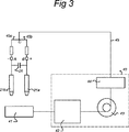
図3は、図2の放射源と連動して使用できるフィードバックシステム40を有するアセンブリを概略的に示している。フィードバックシステム40は、リザーバ25a、25bによって小滴26a、26bとしてそれぞれ集められた導電流体を再利用するように構成されている。図3には、単一のリザーバ41が示されている。フィードバックシステムは、溶解チャンバ42、ポンプ43、およびフィルタ44を有する。溶解チャンバを使用して、リザーバ41によって集められた導電材料を溶解して液体にし、適切なパイプおよびホース45、すなわち、供給ラインを通してノズル21a、21bに向かう輸送に適切な流体となるようにする。接合Cにおいて、供給ライン45は、負端子Aへの第1供給ライン45aおよび正端子Bへの第2供給ライン45bに分かれる。ポンプ43によってこのような輸送が可能となり、一方で、フィルタ44は、液体からコンタミを除去する。溶解チャンバ42、ポンプ43、およびフィルタ44は、単一の流体供給ユニットまたはフィードバックユニット内で結合されてもよいが、また、別個のユニットのアセンブリとしてのフィードバックシステム40を形成してもよい。
FIG. 3 schematically illustrates an assembly having a
コンデンサバンク24に蓄積された放電エネルギーは、コンデンサバンク24の対向する側面に位置する供給ラインの間の高圧差を生じさせる。従って、供給ライン45aおよび45b内の導電液体を介した端子AとBとの間の電気インピーダンスは、高くする必要がある。しかし、実際に高電圧は依然としてフィードバックシステムに到達する。高電圧に応じるために、フィードバックシステム40を二重にし得る。すなわち、各ノズル21a、22bに対して別個の加熱チャンバ42、ポンプ43、およびフィルタ44を設けて、アセンブリ全体での短絡なしにジェット23a、23bを生成することを可能とし得る。さらに、2つのジェット23a、23bのうちの1つに高電圧を与えてもよく、従って、高電圧は2つのフィードバックシステムのうちの1つにのみ到達する。しかし、放射源SO’の操作は、より困難で危険なものとなる。
The discharge energy stored in the
図4は、本発明の一実施形態を備えた、図3に示すアセンブリを概略的に示す。この実施形態において、アセンブリは、高インダクタンスユニット50およびパルスチャージャ51(例えば、パルス同期チャージャ)をさらに含む。高インダクタンスユニット50は、接合A、B、および接合Cの間に位置する。米国特許出願第2006−0011864号に記載されている通り、放電30により生成される電流は、磁界を誘発する。磁界は、衝突によってイオンおよび自由電子が生成されるピンチ(コンプレッション)を生成する。一部の電子は、ピンチ中の原子の伝導帯より低い帯域へと低下し、従って、前述の放射29を生成する。放射源SO’を効率良く操作するために、すなわち、エネルギー損失を最小限に抑えるために、2つのジェット 23a、23b、コンデンサバンク24、および放電30により形成される回路、すなわち「内部回路」のインダクタンスは、可能な限り小さくする必要がある。これは、前述の構成要素間の距離および現象を最小限に抑えることにより達成される。高インダクタンスユニット50は、端子Aおよび接合Cの間、および端子Bおよび接合Cの間の高いインダクタンスを提供するため、この最小限化の特徴をさらに増大させる。従って、フィードバックシステム40は、内部回路から分離される。さらに、高インダクタンスユニット50は、主放電30の前でエネルギー散逸を防ぐ。
FIG. 4 schematically illustrates the assembly shown in FIG. 3 with an embodiment of the present invention. In this embodiment, the assembly further includes a
一実施形態において、パルスチャージャ51は、コンデンサバンク24の一方の側に負に帯電させ、もう一方の側に正に帯電させるように構成される(正負の帯電は大きさの点で等しい)。従って、フィードバックシステム40および供給ライン45の主要部は、接地電位に規定され、高インダクタンスユニット50の存在によってこの電位に留まる。
In one embodiment, the
別の実施形態において、パルスチャージャ51は、コンデンサバンク24の一方の側に正または負に帯電させ、一方で、もう一方の側が接地されるように構成される。この場合は、一実施形態において、高インダクタンスユニットは、接地電位を有するジェット23aを分離せず、パルスチャージャ51により帯電させられる側に接続されるジェット23bのみを分離する。このような実施形態において、ポンプ43は、電気的要因による故障から十分に保護される。
In another embodiment, the
図5は、図4に示す高インダクタンスユニット50の一形態を概略的に示す。高インダクタンスユニット50は、供給ラインの一部をそれぞれ巻線に成形して形成される、各供給ラインのコイル55a、55bを含む。より高いインダクタンス値、従って、より長い高インダクタンスユニットの保持時間を提供するために、そして、導体損失を低減するために、飽和コア56、例えば、強磁性コアをコイル55a、55bにおいて使用し得る。このような飽和コア56を使用することにより、0.01〜10mHのインダクタンスを実現できる。当然のことながら、飽和コア56は、線形の(不飽和の)状態でも作用し得る。適切なインダクタンスは、帯電時間によって決まり、言い換えると、帯電ユニットの有能電力(available power)によって決まる。例えば、2mCの総電荷量、2.4kVの電圧、および10μsの帯電時間により1mHの最小インダクタンスとなるであろう。同様に、より短い帯電時間、すなわち、1μsは、0.01mHの最小インダクタンスにつながるであろう。飽和コア56は、約5〜100kHzの周波数、すなわち、EUV源に対して妥当な周波数での操作を可能とする強磁性材料、例えば、METGLAS 2605 C0のようなナノ結晶合金を含み得る。さらに、そのような合金は、高い導磁性、すなわち、50、000〜100、000、および約400〜450℃という比較的高いキュリー温度を有する。別の実施形態において、飽和コア56は、別の強磁性材料、すなわちフェライトを含む。
FIG. 5 schematically shows an embodiment of the
2つのコイル51a、51bの間の飽和コア56の概略的な表示は、飽和コア56が2つのコイル51a、51bの間に配置されるという意味ではないことが理解されるべきである。実際、両コイル51a、51bは、通常、飽和コア56に巻装される。あるいは、両コイル51a、51bはそれぞれに飽和コア56を備えてもよい。
It should be understood that the schematic representation of the saturated
さらに、図4に記載された実施形態において、2つのジェット23a、23bのうちの1つのみが分離され、コイル51a、51bのうちの1つのみが存在することが理解されるべきである。すなわち、例えば、ジェット23aが帯電し、かつジェット23bが接地電位に維持されると、ジェット23aのみが、コイル51aによって誘導的に分離されることになる。
Furthermore, it should be understood that in the embodiment described in FIG. 4, only one of the two
すでに小滴(例えば、小滴26a、26b)に分解された導電材料を集める位置にリザーバ(例えば図2のリザーバ25a、25b)を配置して内部回路をフィードバックシステムから分離する代わりに、分離のための異なる配置を使用してもよい。この配置において、図6に示されるように、追加の高インダクタンスユニット60は、リザーバ62a、62bとフィードバックライン63a、63bとの間に位置付けられる。フィードバックライン63a、63bは、リザーバ62a、62bによってそれぞれ集められた材料をフィードバックシステム40に向けて輸送する。フィードバックライン63a、63bは、図6に示されるように、追加の高インダクタンスユニット60とフィードバックシステム40に位置付けられた接合に接続されて単一のフィードバックライン63を形成し得るが、別々のラインのままでもよい。
Instead of placing a reservoir (eg,
リザーバ62a、62bは、図2のジェット23a、23bといった個別の電極を形成する導電材料が小滴に分解される位置に配される必要はないものの、この形態において、単一のリザーバに材料を集めることは可能ではない。そのような場合には、内部回路が短絡化されるであろう。
図6に示した形態において、追加の高インダクタンスユニット60は、2つのコイル61a、61bを含む。各コイルは、リザーバ62a、62bのそれぞれに集められた材料をフィードバックシステム40に向けて輸送するフィードバックラインに対応する。各フィードバックラインに対するコイル61a、61bは、フィードバックラインの一部をそれぞれ巻線に成形することにより形成される。より高いインダクタンス値、従って、より長い高インダクタンスユニットの保持時間を提供するために、そして、導体損失を低減するために、飽和コア64、例えば、強磁性コアをコイル61a、61bにおいて使用し得る。このような飽和コア64を使用することにより、0.01〜10mHのインダクタンスを実現できる。当然のことながら、飽和コア64は、線形の(不飽和の)状態でも作用し得る。適切なインダクタンスは、帯電時間によって決まり、言い換えると、帯電ユニットの有能電力によって決まる。例えば、2mCの総電荷量、2.4kVの電圧、および10μsの帯電時間により1mHの最小インダクタンスとなるであろう。同様に、より短い帯電時間、すなわち、1μsは、0.01mHの最小インダクタンスにつながるであろう。飽和コア64は、約5〜100kHzの周波数、すなわち、EUV源に対して妥当な周波数での操作を可能とするMETGLAS 2605 C0のようなナノ結晶合金を含み得る。さらに、そのような合金は、高い導磁性、すなわち、50、000〜100、000、および約400〜450℃という比較的高いキュリー温度を有する。別の実施形態において、飽和コア64はフェライトを含む。
In the form shown in FIG. 6, the additional high inductance unit 60 includes two coils 61a and 61b. Each coil corresponds to a feedback line that transports the material collected in each of the
この場合もやはり、2つのコイル61a、61bの間の飽和コア64の概略的な表示は、飽和コア64が2つのコイル61a、61bの間に配置という意味ではないことが理解されるべきである。実際、両コイル51a、51bは、通常、飽和コア56に巻装される。あるいは、両コイル61a、61bはそれぞれに飽和コア64を備えてもよい。
Again, it should be understood that the schematic representation of the saturated core 64 between the two coils 61a, 61b does not mean that the saturated core 64 is located between the two coils 61a, 61b. . Actually, both the coils 51 a and 51 b are usually wound around the saturated
本明細書において、IC製造におけるリソグラフィ装置の使用について具体的な言及がなされているが、本明細書記載のリソグラフィ装置が、集積光学システム、磁気ドメインメモリ用のガイダンスパターンおよび検出パターン、フラットパネルディスプレイ、液晶ディスプレイ(LCD)、薄膜磁気ヘッド等の製造といった他の用途を有し得ることが理解されるべきである。当然のことながら、そのような別の用途においては、本明細書で使用される「ウェーハ」または「ダイ」という用語はすべて、それぞれより一般的な「基板」または「ターゲット部分」という用語と同義であるとみなしてよい。本明細書に記載した基板は、露光の前後を問わず、例えば、トラック(通常、基板にレジスト層を塗布し、かつ露光されたレジストを現像するツール)、メトロロジーツール、および/またはインスペクションツールで処理されてもよい。適用可能な場合には、本明細書中の開示内容を上記のような基板プロセシングツールおよびその他の基板プロセシングツールに適用してもよい。さらに基板は、例えば、多層ICを作るために複数回処理されてもよいので、本明細書で使用される基板という用語は、すでに多重処理層を包含している基板を表すものとしてもよい。 Although specific reference is made herein to the use of a lithographic apparatus in IC manufacturing, the lithographic apparatus described herein can be used in integrated optical systems, guidance and detection patterns for magnetic domain memories, flat panel displays, and the like. It should be understood that other applications such as the manufacture of liquid crystal displays (LCDs), thin film magnetic heads, etc. may be used. Of course, in such other applications, the terms “wafer” or “die” as used herein are all synonymous with the more general terms “substrate” or “target portion”, respectively. May be considered. The substrate described herein can be used, for example, before or after exposure, such as a track (usually a tool for applying a resist layer to the substrate and developing the exposed resist), a metrology tool, and / or an inspection tool. May be processed. Where applicable, the disclosure herein may be applied to substrate processing tools such as those described above and other substrate processing tools. Further, since the substrate may be processed multiple times, for example, to make a multi-layer IC, the term substrate as used herein may refer to a substrate that already contains multiple processing layers.
光リソグラフィの関連での本発明の実施形態の使用について上述のとおり具体的な言及がなされたが、当然のことながら、本発明は、他の用途、例えば、インプリントリソグラフィに使われてもよく、さらに状況が許すのであれば、光リソグラフィに限定されることはない。インプリントリソグラフィにおいては、パターニングデバイス内のトポグラフィによって、基板上に創出されるパターンが定義される。パターニングデバイスのトポグラフィは、基板に供給されたレジスト層の中にプレス加工され、基板上では、電磁放射、熱、圧力、またはそれらの組合せによってレジストは硬化される。パターニングデバイスは、レジストが硬化した後、レジスト内にパターンを残してレジストの外へ移動される。 Although specific reference has been made to the use of embodiments of the present invention in the context of optical lithography as described above, it will be appreciated that the present invention may be used in other applications, such as imprint lithography. And if the situation allows, it is not limited to photolithography. In imprint lithography, the topography within the patterning device defines the pattern that is created on the substrate. The topography of the patterning device is pressed into a resist layer supplied to the substrate, whereupon the resist is cured by electromagnetic radiation, heat, pressure, or a combination thereof. The patterning device is moved out of the resist leaving a pattern in it after the resist is cured.
本明細書で使用される「放射」および「ビーム」という用語は、紫外線(UV)(例えば、365nm、355nm、248nm、193nm、157nm、または126nmの波長、またはおよそこれらの値の波長を有する)、および極端紫外線(EUV)(例えば、5〜20nmの範囲の波長を有する)、ならびにイオンビームや電子ビームなどの微粒子ビームを含むあらゆる種類の電磁放射を包含している。 As used herein, the terms “radiation” and “beam” are ultraviolet (UV) (eg, having a wavelength of 365 nm, 355 nm, 248 nm, 193 nm, 157 nm, or 126 nm, or approximately these values) , And extreme ultraviolet (EUV) (eg, having a wavelength in the range of 5-20 nm), and all types of electromagnetic radiation, including particulate beams such as ion beams and electron beams.
「レンズ」という用語は、文脈によっては、屈折、反射、磁気、電磁気、および静電型光コンポーネントを含む様々な種類の光コンポーネントのいずれか1つまたはこれらの組合せを指すことができる。 The term “lens” can refer to any one or combination of various types of optical components, including refractive, reflective, magnetic, electromagnetic, and electrostatic optical components, depending on the context.
以上、本発明の具体的な実施形態を説明してきたが、本発明は、上述以外の態様で実施できることが明らかである。 While specific embodiments of the invention have been described above, it will be appreciated that the invention may be practiced otherwise than as described.
上記の説明は、制限ではなく例示を意図したものである。したがって、当業者には明らかなように、添付の特許請求の範囲を逸脱することなく本記載の発明に変更を加えてもよい。 The above description is intended to be illustrative rather than limiting. Thus, it will be apparent to one skilled in the art that modifications may be made to the invention as described without departing from the scope of the claims set out below.
Claims (40)
第1電極および第2電極であって、前記第1電極および前記第2電極の間にガス媒体におけるプラズマ点火を可能とする距離をおいて構成された第1電極および第2電極、
前記第1電極への第1端子および前記第2電極への第2端子と電気的に接続されるコンデンサバンクであって、前記プラズマ点火に必要とされる放電エネルギーを蓄積するように構成され、前記第1電極、前記第2電極、および前記コンデンサバンクは電気回路を形成し、少なくとも前記第1電極は、第1供給ラインを介して供給される導電流体によって形成されたコンデンサバンク、
時間的に変化する規則で前記コンデンサバンクに帯電させるように構成された前記第1端子および/または前記第2端子に接続されたチャージャ、および
前記第1供給ラインにおける前記第1端子の上流に、前記電気回路を電気的に分離するように設けられた第1高インダクタンスユニット
を含み、
前記第1高インダクタンスユニットは、前記第1供給ラインの第1コイル状部分を含む、装置。An apparatus for generating radiation by an electrically operated discharge, the apparatus comprising:
A first electrode and a second electrode, wherein the first electrode and the second electrode are arranged at a distance allowing a plasma ignition in a gas medium between the first electrode and the second electrode;
A capacitor bank electrically connected to the first terminal to the first electrode and the second terminal to the second electrode, configured to store discharge energy required for the plasma ignition; The first electrode, the second electrode, and the capacitor bank form an electric circuit, and at least the first electrode is a capacitor bank formed by a conductive fluid supplied through a first supply line;
Upstream of the first terminal in the first supply line and the charger connected to the first terminal and / or the second terminal configured to charge the capacitor bank with a time-varying rule; look including the first high inductance unit provided to electrically isolate said electrical circuit,
The first high inductance unit includes a first coiled portion of the first supply line .
前記リザーバに接続され、集められた前記材料を溶解して前記材料の溶解物を形成するように構成された溶解チャンバ、
前記第1供給ラインに接続され、前記材料の前記溶解物からコンタミを除去するように構成されたフィルタ、および
前記溶解チャンバから前記フィルタに向けて前記溶解物を送り込むように構成されたポンプを含む、請求項9に記載の装置。The apparatus includes a reservoir configured to collect the jet of the material and a feedback system configured to feed back the material collected in the reservoir toward the first supply line. The feedback system is
A dissolution chamber connected to the reservoir and configured to dissolve the collected material to form a lysate of the material;
A filter connected to the first supply line and configured to remove contamination from the lysate of the material; and a pump configured to pump the lysate from the lysis chamber toward the filter. The apparatus according to claim 9 .
前記材料の前記第2ジェットを集めるように構成された第2リザーバ、および
第1フィードバックラインを介して前記第1リザーバに、および、第2フィードバックラインを介して前記第2リザーバに接続されたフィードバックシステムであって、前記第1供給ラインおよび/または前記第2供給ラインに向けて、前記第1リザーバおよび前記第2リザーバに集められた前記材料をフィードバックするように構成されたフィードバックシステム、を含み、前記フィードバックシステムは、
前記第1リザーバおよび前記第2リザーバに接続され、集められたそれぞれの前記材料を溶解して前記材料の溶解物を形成するように構成された溶解チャンバ、
前記第1供給ラインおよび/または前記第2供給ラインに接続され、前記材料の前記溶解物からコンタミを除去するように構成されたフィルタ、および
前記溶解チャンバから前記フィルタに向けて前記溶解物を送り込むように構成されたポンプを含む、装置であって、
前記装置は、前記第1フィードバックラインにおける前記第1リザーバの下流に、第3高インダクタンスユニットをさらに備え、前記第2フィードバックラインにおける前記第2リザーバの下流に、第4高インダクタンスユニットをさらに備える、請求項11に記載の装置。A first reservoir configured to collect the first jet of the material;
A second reservoir configured to collect the second jet of material; and a feedback connected to the first reservoir via a first feedback line and to the second reservoir via a second feedback line. A feedback system configured to feed back the material collected in the first reservoir and the second reservoir toward the first supply line and / or the second supply line; The feedback system is
A dissolution chamber connected to the first reservoir and the second reservoir and configured to dissolve each collected material to form a lysate of the material;
A filter connected to the first supply line and / or the second supply line and configured to remove contamination from the lysate of the material, and pumping the lysate from the lysis chamber toward the filter An apparatus comprising a pump configured to
The apparatus further includes a third high inductance unit downstream of the first reservoir in the first feedback line, and further includes a fourth high inductance unit downstream of the second reservoir in the second feedback line. The apparatus of claim 11 .
パターニングデバイスを支持するように構成されたサポートであって、前記パターニングデバイスが、前記放射ビームの断面にパターンを付与して、パターン付き放射ビームを
形成するように構成されているサポート、
基板を保持するように構成された基板テーブル、および
前記基板のターゲット部分に前記パターン付き放射ビームを投影するように構成された投影システム、を含み、前記照明システムは、電動放電により放射を生成する装置を含むリソグラフィ装置であって、前記装置は、
第1電極および第2電極であって、前記第1および第2電極の間にガス媒体におけるプラズマ点火を可能とする距離をおいて構成された第1電極および第2電極、および
前記第1電極への第1端子および前記第2電極への第2端子と電気的に接続されるコンデンサバンクであって、前記プラズマ点火に必要とされる放電エネルギーを蓄積するように構成され、前記第1電極、前記第2電極、および前記コンデンサバンクは電気回路を形成し、少なくとも前記第1電極は、第1供給ラインを介して供給される導電流体によって形成されたコンデンサバンク、
時間的に変化する規則で前記コンデンサバンクに帯電させるように構成された前記第1端子および/または前記第2端子 に接続されたチャージャ、および
前記第1供給ラインにおける前記第1端子の上流に、前記電気回路を電気的に分離するように構成された第1高インダクタンスユニット
を含み、
前記第1高インダクタンスユニットは、前記第1供給ラインの第1コイル状部分を含む、リソグラフィ装置。An illumination system configured to condition the radiation beam;
A support configured to support a patterning device, wherein the patterning device is configured to impart a pattern to a cross-section of the radiation beam to form a patterned radiation beam;
A substrate table configured to hold a substrate; and a projection system configured to project the patterned radiation beam onto a target portion of the substrate, wherein the illumination system generates radiation by an electric discharge A lithographic apparatus comprising an apparatus, the apparatus comprising:
A first electrode and a second electrode, the first electrode and the second electrode being configured with a distance between the first and second electrodes enabling a plasma ignition in a gas medium; and the first electrode A capacitor bank electrically connected to the first terminal to the second electrode and the second terminal to the second electrode, the capacitor bank being configured to store discharge energy required for the plasma ignition, The second electrode and the capacitor bank form an electrical circuit, at least the first electrode being formed by a conductive fluid supplied via a first supply line,
Upstream of the first terminal in the first supply line and the charger connected to the first terminal and / or the second terminal configured to charge the capacitor bank with a time-varying rule; look including the first high inductance unit that is configured to electrically isolate said electrical circuit,
The lithographic apparatus , wherein the first high inductance unit includes a first coiled portion of the first supply line .
第1電極および第2電極であって、前記第1および第2電極の間にガス媒体におけるプラズマ点火を可能とする距離をおいて構成された第1電極および第2電極、および
前記第1電極への第1端子および前記第2電極への第2端子と電気的に接続されるコンデンサバンクであって、前記プラズマ点火に必要とされる放電エネルギーを蓄積するように構成され、前記第1電極、前記第2電極、および前記コンデンサバンクは電気回路を形成し、前記第1電極は、第1供給ラインを介して供給される導電流体によって形成され、
前記第2電極は、第2供給ラインを介して供給される導電流体によって形成され、前記第1供給ラインは、材料が第1ジェットの形状をとる前記第1電極を提供するように構成される第1ノズルを含み、前記第2供給ラインは、材料が第2ジェットの形状をとる前記第2電極を提供するように構成される第2ノズルを含むコンデンサバンク、
時間的に変化する規則で前記コンデンサバンクに帯電させるように構成されたチャージャ、
前記第1供給ラインにおける前記第1端子の上流に設けられた第1高インダクタンスユニットであって、前記第1供給ラインの第1コイル状部分を含む、第1高インダクタンスユニット、および
前記第2供給ラインにおける前記第2端子の上流に設けられた第2高インダクタンスユニットであって、前記第2供給ラインの第2コイル状部分を含む、第2高インダクタンスユニット
を含む、装置。An apparatus for generating radiation by electric discharge, the apparatus comprising:
A first electrode and a second electrode, the first electrode and the second electrode being configured with a distance between the first and second electrodes enabling a plasma ignition in a gas medium; and the first electrode A capacitor bank electrically connected to the first terminal to the second electrode and the second terminal to the second electrode, the capacitor bank being configured to store discharge energy required for the plasma ignition, The second electrode and the capacitor bank form an electrical circuit, and the first electrode is formed by a conductive fluid supplied through a first supply line;
The second electrode is formed by a conductive fluid supplied through a second supply line, and the first supply line is configured to provide the first electrode in which the material takes the form of a first jet. A capacitor bank including a first nozzle, and wherein the second supply line includes a second nozzle configured to provide the second electrode in the form of a second jet of material.
A charger configured to charge the capacitor bank with a time-varying rule;
A first high inductance unit provided upstream of the first terminal in the first supply line, the first high inductance unit including a first coiled portion of the first supply line; and the second supply. An apparatus comprising a second high inductance unit provided in the line upstream of the second terminal, the second high inductance unit including a second coiled portion of the second supply line.
第1電極および第2電極であって、前記第1および第2電極の間にガス媒体におけるプラズマ点火を可能とする距離をおいて構成された第1電極および第2電極、および
前記第1電極への第1端子および前記第2電極への第2端子と電気的に接続されるコンデンサバンクであって、前記プラズマ点火に必要とされる放電エネルギーを蓄積するように構成され、前記第1電極、前記第2電極、および前記コンデンサバンクは電気回路を形成し、少なくとも前記第1電極は、第1供給ラインを介して供給される導電流体によって形成されたコンデンサバンク、
時変的に前記コンデンサバンクに帯電させるように構成された前記第1端子および/または前記第2端子に接続されたチャージャ、および
前記第1供給ラインにおける前記第1端子の上流に、前記電気回路を電気的に分離するように設けられた第1高インダクタンスユニットを含み、
前記放射からの放射ビームを調整すること、
前記放射ビームにパターンを付与すること、および
基板のターゲット部分に前記パターン付き放射ビームを投影すること、
を含み、
前記第1高インダクタンスユニットは、前記第1供給ラインの第1コイル状部分を含む、デバイス製造方法。Providing radiation from a radiation source configured to generate radiation by an electric discharge, the radiation source comprising:
A first electrode and a second electrode, the first electrode and the second electrode being configured with a distance between the first and second electrodes enabling a plasma ignition in a gas medium; and the first electrode A capacitor bank electrically connected to the first terminal to the second electrode and the second terminal to the second electrode, the capacitor bank being configured to store discharge energy required for the plasma ignition, The second electrode and the capacitor bank form an electrical circuit, at least the first electrode being formed by a conductive fluid supplied via a first supply line,
A charger connected to the first terminal and / or the second terminal configured to charge the capacitor bank in a time-varying manner; and the electrical circuit upstream of the first terminal in the first supply line Including a first high inductance unit provided to electrically isolate
Adjusting the radiation beam from the radiation;
Applying a pattern to the radiation beam; and projecting the patterned radiation beam onto a target portion of a substrate;
Only including,
The device manufacturing method , wherein the first high inductance unit includes a first coiled portion of the first supply line .
Applications Claiming Priority (3)
| Application Number | Priority Date | Filing Date | Title |
|---|---|---|---|
| US11/417,211 | 2006-05-04 | ||
| US11/417,211 US7557366B2 (en) | 2006-05-04 | 2006-05-04 | Radiation generating device, lithographic apparatus, device manufacturing method and device manufactured thereby |
| PCT/NL2007/050187 WO2007129891A1 (en) | 2006-05-04 | 2007-04-27 | Radiation generating device, lithographic apparatus, device manufacturing method and device manufactured thereby |
Publications (2)
| Publication Number | Publication Date |
|---|---|
| JP2009535839A JP2009535839A (en) | 2009-10-01 |
| JP4987966B2 true JP4987966B2 (en) | 2012-08-01 |
Family
ID=38324152
Family Applications (1)
| Application Number | Title | Priority Date | Filing Date |
|---|---|---|---|
| JP2009509462A Expired - Fee Related JP4987966B2 (en) | 2006-05-04 | 2007-04-27 | Radiation generating device, lithographic apparatus, device manufacturing method and device manufactured thereby |
Country Status (8)
| Country | Link |
|---|---|
| US (1) | US7557366B2 (en) |
| EP (1) | EP2014141B1 (en) |
| JP (1) | JP4987966B2 (en) |
| KR (1) | KR101023797B1 (en) |
| CN (1) | CN101438631B (en) |
| AT (1) | ATE547924T1 (en) |
| TW (1) | TWI368110B (en) |
| WO (1) | WO2007129891A1 (en) |
Families Citing this family (7)
| Publication number | Priority date | Publication date | Assignee | Title |
|---|---|---|---|---|
| NL1036595A1 (en) * | 2008-02-28 | 2009-08-31 | Asml Netherlands Bv | Device constructed and arranged to generate radiation, lithographic apparatus, and device manufacturing method. |
| KR200458311Y1 (en) * | 2009-12-24 | 2012-02-15 | 김수선 | Injection nozzle for water jet loom |
| JP6039665B2 (en) | 2011-07-13 | 2016-12-07 | エーエスエムエル ネザーランズ ビー.ブイ. | Power supply for discharge generated plasma EUV source |
| RU2496282C1 (en) * | 2012-02-15 | 2013-10-20 | Общество С Ограниченной Ответственностью "Эуф Лабс" | Device and method for emission generation from discharge plasma |
| WO2019083722A1 (en) * | 2017-10-24 | 2019-05-02 | Cymer, Llc | Method of and apparatus for extending electrode life in a laser chamber |
| JP7381728B2 (en) * | 2019-10-11 | 2023-11-15 | サイマー リミテッド ライアビリティ カンパニー | Conductive material for discharge laser |
| DE102022104850A1 (en) | 2022-03-01 | 2023-09-07 | Magnetec Gmbh | Inductive component, method for producing an inductive component, use of an inductive component and motor vehicle |
Family Cites Families (12)
| Publication number | Priority date | Publication date | Assignee | Title |
|---|---|---|---|---|
| GB1368090A (en) * | 1971-08-02 | 1974-09-25 | Messner G | Process for the extraction of aluminium from its alloys |
| US5204506A (en) * | 1987-12-07 | 1993-04-20 | The Regents Of The University Of California | Plasma pinch surface treating apparatus and method of using same |
| US4889605A (en) * | 1987-12-07 | 1989-12-26 | The Regents Of The University Of California | Plasma pinch system |
| JPH05161340A (en) * | 1991-11-21 | 1993-06-25 | Ishikawajima Harima Heavy Ind Co Ltd | Molten metal circulating pump |
| JP3307988B2 (en) * | 1992-07-17 | 2002-07-29 | 株式会社ニコン | Projection exposure method and apparatus |
| US5963616A (en) * | 1997-03-11 | 1999-10-05 | University Of Central Florida | Configurations, materials and wavelengths for EUV lithium plasma discharge lamps |
| US6815700B2 (en) * | 1997-05-12 | 2004-11-09 | Cymer, Inc. | Plasma focus light source with improved pulse power system |
| US6408052B1 (en) | 2000-04-06 | 2002-06-18 | Mcgeoch Malcolm W. | Z-pinch plasma X-ray source using surface discharge preionization |
| EP1305984B1 (en) * | 2000-07-28 | 2010-11-24 | Jettec AB | Method and apparatus for generating x-ray radiation |
| DE10342239B4 (en) | 2003-09-11 | 2018-06-07 | Fraunhofer-Gesellschaft zur Förderung der angewandten Forschung e.V. | Method and apparatus for generating extreme ultraviolet or soft x-ray radiation |
| US7208746B2 (en) * | 2004-07-14 | 2007-04-24 | Asml Netherlands B.V. | Radiation generating device, lithographic apparatus, device manufacturing method and device manufactured thereby |
| JP4429302B2 (en) * | 2005-09-23 | 2010-03-10 | エーエスエムエル ネザーランズ ビー.ブイ. | Electromagnetic radiation source, lithographic apparatus, device manufacturing method, and device manufactured by the manufacturing method |
-
2006
- 2006-05-04 US US11/417,211 patent/US7557366B2/en not_active Expired - Fee Related
-
2007
- 2007-04-23 TW TW096114233A patent/TWI368110B/en not_active IP Right Cessation
- 2007-04-27 KR KR1020087027018A patent/KR101023797B1/en not_active IP Right Cessation
- 2007-04-27 AT AT07747411T patent/ATE547924T1/en active
- 2007-04-27 JP JP2009509462A patent/JP4987966B2/en not_active Expired - Fee Related
- 2007-04-27 WO PCT/NL2007/050187 patent/WO2007129891A1/en active Application Filing
- 2007-04-27 EP EP07747411A patent/EP2014141B1/en not_active Not-in-force
- 2007-04-27 CN CN200780016104.XA patent/CN101438631B/en not_active Expired - Fee Related
Also Published As
| Publication number | Publication date |
|---|---|
| TW200807165A (en) | 2008-02-01 |
| KR20090006166A (en) | 2009-01-14 |
| ATE547924T1 (en) | 2012-03-15 |
| EP2014141B1 (en) | 2012-02-29 |
| JP2009535839A (en) | 2009-10-01 |
| CN101438631B (en) | 2011-05-11 |
| TWI368110B (en) | 2012-07-11 |
| CN101438631A (en) | 2009-05-20 |
| KR101023797B1 (en) | 2011-03-22 |
| US20080067453A1 (en) | 2008-03-20 |
| WO2007129891A1 (en) | 2007-11-15 |
| US7557366B2 (en) | 2009-07-07 |
| EP2014141A1 (en) | 2009-01-14 |
Similar Documents
| Publication | Publication Date | Title |
|---|---|---|
| US9939737B2 (en) | Electrostatic clamp | |
| JP4987966B2 (en) | Radiation generating device, lithographic apparatus, device manufacturing method and device manufactured thereby | |
| WO2009129960A1 (en) | Lithographic apparatus, device manufacturing method, cleaning system and method for cleaning a patterning device | |
| EP2875404A1 (en) | Electrostatic clamp, lithographic apparatus and method | |
| WO2008140305A1 (en) | Radiation generating device, lithographic apparatus, device manufacturing method and device manufactured thereby | |
| JP5069367B2 (en) | Fast ion reduction in plasma radiation sources. | |
| JP4841239B2 (en) | Lithographic apparatus and device manufacturing method | |
| JP2007517396A (en) | Lithographic apparatus, radiation source comprising a debris mitigation system, and method for mitigating debris particles in a lithographic apparatus | |
| US7759663B1 (en) | Self-shading electrodes for debris suppression in an EUV source | |
| US8362444B2 (en) | Plasma radiation source, method of forming plasma radiation, apparatus for projecting a pattern from a patterning device onto a substrate and device manufacturing method | |
| US20060011864A1 (en) | Radiation generating device, lithographic apparatus, device manufacturing method and device manufactured thereby | |
| JP5005748B2 (en) | Non-contact cleaning system, lithographic apparatus, and device manufacturing method | |
| JP4828985B2 (en) | Lithographic apparatus and device manufacturing method | |
| US20110007289A1 (en) | Device constructed and arranged to generate radiation, lithographic apparatus, and device manufacturing method | |
| WO2021063722A1 (en) | A cleaning device, a lithography apparatus, a method of removing water or other contaminant and a device manufacturing method |
Legal Events
| Date | Code | Title | Description |
|---|---|---|---|
| A131 | Notification of reasons for refusal |
Free format text: JAPANESE INTERMEDIATE CODE: A131 Effective date: 20110520 |
|
| A521 | Request for written amendment filed |
Free format text: JAPANESE INTERMEDIATE CODE: A523 Effective date: 20110818 |
|
| TRDD | Decision of grant or rejection written | ||
| A01 | Written decision to grant a patent or to grant a registration (utility model) |
Free format text: JAPANESE INTERMEDIATE CODE: A01 Effective date: 20120328 |
|
| A01 | Written decision to grant a patent or to grant a registration (utility model) |
Free format text: JAPANESE INTERMEDIATE CODE: A01 |
|
| A61 | First payment of annual fees (during grant procedure) |
Free format text: JAPANESE INTERMEDIATE CODE: A61 Effective date: 20120425 |
|
| R150 | Certificate of patent or registration of utility model |
Free format text: JAPANESE INTERMEDIATE CODE: R150 |
|
| FPAY | Renewal fee payment (event date is renewal date of database) |
Free format text: PAYMENT UNTIL: 20150511 Year of fee payment: 3 |
|
| LAPS | Cancellation because of no payment of annual fees |