JP4985853B2 - Optical signal generator and adjustment method thereof - Google Patents
Optical signal generator and adjustment method thereof Download PDFInfo
- Publication number
- JP4985853B2 JP4985853B2 JP2010543724A JP2010543724A JP4985853B2 JP 4985853 B2 JP4985853 B2 JP 4985853B2 JP 2010543724 A JP2010543724 A JP 2010543724A JP 2010543724 A JP2010543724 A JP 2010543724A JP 4985853 B2 JP4985853 B2 JP 4985853B2
- Authority
- JP
- Japan
- Prior art keywords
- single mode
- mode laser
- optical signal
- modulation
- signal
- Prior art date
- Legal status (The legal status is an assumption and is not a legal conclusion. Google has not performed a legal analysis and makes no representation as to the accuracy of the status listed.)
- Expired - Fee Related
Links
- 230000003287 optical effect Effects 0.000 title claims description 132
- 238000000034 method Methods 0.000 title claims description 36
- 230000008033 biological extinction Effects 0.000 claims description 75
- 230000010355 oscillation Effects 0.000 claims description 25
- 239000000758 substrate Substances 0.000 claims description 24
- 230000007274 generation of a signal involved in cell-cell signaling Effects 0.000 claims description 10
- 238000012544 monitoring process Methods 0.000 claims description 7
- 230000005540 biological transmission Effects 0.000 description 30
- 230000008859 change Effects 0.000 description 19
- 239000004065 semiconductor Substances 0.000 description 18
- 230000008569 process Effects 0.000 description 14
- 238000002834 transmittance Methods 0.000 description 8
- 230000008901 benefit Effects 0.000 description 7
- 238000004891 communication Methods 0.000 description 7
- 239000013307 optical fiber Substances 0.000 description 5
- BJQHLKABXJIVAM-UHFFFAOYSA-N bis(2-ethylhexyl) phthalate Chemical compound CCCCC(CC)COC(=O)C1=CC=CC=C1C(=O)OCC(CC)CCCC BJQHLKABXJIVAM-UHFFFAOYSA-N 0.000 description 4
- 238000010586 diagram Methods 0.000 description 4
- 230000000694 effects Effects 0.000 description 4
- 239000002131 composite material Substances 0.000 description 3
- 230000006866 deterioration Effects 0.000 description 3
- 230000004048 modification Effects 0.000 description 3
- 238000012986 modification Methods 0.000 description 3
- 239000010453 quartz Substances 0.000 description 3
- VYPSYNLAJGMNEJ-UHFFFAOYSA-N silicon dioxide Inorganic materials O=[Si]=O VYPSYNLAJGMNEJ-UHFFFAOYSA-N 0.000 description 3
- 230000004913 activation Effects 0.000 description 2
- 238000013459 approach Methods 0.000 description 2
- 239000000835 fiber Substances 0.000 description 2
- 238000004519 manufacturing process Methods 0.000 description 2
- 230000000737 periodic effect Effects 0.000 description 2
- 238000000411 transmission spectrum Methods 0.000 description 2
- 229910001218 Gallium arsenide Inorganic materials 0.000 description 1
- 238000010521 absorption reaction Methods 0.000 description 1
- 230000015556 catabolic process Effects 0.000 description 1
- 238000006243 chemical reaction Methods 0.000 description 1
- 239000012792 core layer Substances 0.000 description 1
- 230000003247 decreasing effect Effects 0.000 description 1
- 238000006731 degradation reaction Methods 0.000 description 1
- 238000001514 detection method Methods 0.000 description 1
- 239000006185 dispersion Substances 0.000 description 1
- 238000003780 insertion Methods 0.000 description 1
- 230000037431 insertion Effects 0.000 description 1
- 238000002955 isolation Methods 0.000 description 1
- 230000007246 mechanism Effects 0.000 description 1
- 230000010363 phase shift Effects 0.000 description 1
- 238000010791 quenching Methods 0.000 description 1
- 230000004044 response Effects 0.000 description 1
- 230000002441 reversible effect Effects 0.000 description 1
- 230000000630 rising effect Effects 0.000 description 1
- 230000009466 transformation Effects 0.000 description 1
Images


Classifications
-
- H—ELECTRICITY
- H01—ELECTRIC ELEMENTS
- H01S—DEVICES USING THE PROCESS OF LIGHT AMPLIFICATION BY STIMULATED EMISSION OF RADIATION [LASER] TO AMPLIFY OR GENERATE LIGHT; DEVICES USING STIMULATED EMISSION OF ELECTROMAGNETIC RADIATION IN WAVE RANGES OTHER THAN OPTICAL
- H01S5/00—Semiconductor lasers
- H01S5/02—Structural details or components not essential to laser action
- H01S5/026—Monolithically integrated components, e.g. waveguides, monitoring photo-detectors, drivers
-
- G—PHYSICS
- G02—OPTICS
- G02F—OPTICAL DEVICES OR ARRANGEMENTS FOR THE CONTROL OF LIGHT BY MODIFICATION OF THE OPTICAL PROPERTIES OF THE MEDIA OF THE ELEMENTS INVOLVED THEREIN; NON-LINEAR OPTICS; FREQUENCY-CHANGING OF LIGHT; OPTICAL LOGIC ELEMENTS; OPTICAL ANALOGUE/DIGITAL CONVERTERS
- G02F1/00—Devices or arrangements for the control of the intensity, colour, phase, polarisation or direction of light arriving from an independent light source, e.g. switching, gating or modulating; Non-linear optics
- G02F1/01—Devices or arrangements for the control of the intensity, colour, phase, polarisation or direction of light arriving from an independent light source, e.g. switching, gating or modulating; Non-linear optics for the control of the intensity, phase, polarisation or colour
- G02F1/0102—Constructional details, not otherwise provided for in this subclass
-
- G—PHYSICS
- G02—OPTICS
- G02F—OPTICAL DEVICES OR ARRANGEMENTS FOR THE CONTROL OF LIGHT BY MODIFICATION OF THE OPTICAL PROPERTIES OF THE MEDIA OF THE ELEMENTS INVOLVED THEREIN; NON-LINEAR OPTICS; FREQUENCY-CHANGING OF LIGHT; OPTICAL LOGIC ELEMENTS; OPTICAL ANALOGUE/DIGITAL CONVERTERS
- G02F2201/00—Constructional arrangements not provided for in groups G02F1/00 - G02F7/00
- G02F2201/58—Arrangements comprising a monitoring photodetector
-
- G—PHYSICS
- G02—OPTICS
- G02F—OPTICAL DEVICES OR ARRANGEMENTS FOR THE CONTROL OF LIGHT BY MODIFICATION OF THE OPTICAL PROPERTIES OF THE MEDIA OF THE ELEMENTS INVOLVED THEREIN; NON-LINEAR OPTICS; FREQUENCY-CHANGING OF LIGHT; OPTICAL LOGIC ELEMENTS; OPTICAL ANALOGUE/DIGITAL CONVERTERS
- G02F2203/00—Function characteristic
- G02F2203/20—Intrinsic phase difference, i.e. optical bias, of an optical modulator; Methods for the pre-set thereof
-
- G—PHYSICS
- G02—OPTICS
- G02F—OPTICAL DEVICES OR ARRANGEMENTS FOR THE CONTROL OF LIGHT BY MODIFICATION OF THE OPTICAL PROPERTIES OF THE MEDIA OF THE ELEMENTS INVOLVED THEREIN; NON-LINEAR OPTICS; FREQUENCY-CHANGING OF LIGHT; OPTICAL LOGIC ELEMENTS; OPTICAL ANALOGUE/DIGITAL CONVERTERS
- G02F2203/00—Function characteristic
- G02F2203/21—Thermal instability, i.e. DC drift, of an optical modulator; Arrangements or methods for the reduction thereof
-
- G—PHYSICS
- G02—OPTICS
- G02F—OPTICAL DEVICES OR ARRANGEMENTS FOR THE CONTROL OF LIGHT BY MODIFICATION OF THE OPTICAL PROPERTIES OF THE MEDIA OF THE ELEMENTS INVOLVED THEREIN; NON-LINEAR OPTICS; FREQUENCY-CHANGING OF LIGHT; OPTICAL LOGIC ELEMENTS; OPTICAL ANALOGUE/DIGITAL CONVERTERS
- G02F2203/00—Function characteristic
- G02F2203/50—Phase-only modulation
-
- G—PHYSICS
- G02—OPTICS
- G02F—OPTICAL DEVICES OR ARRANGEMENTS FOR THE CONTROL OF LIGHT BY MODIFICATION OF THE OPTICAL PROPERTIES OF THE MEDIA OF THE ELEMENTS INVOLVED THEREIN; NON-LINEAR OPTICS; FREQUENCY-CHANGING OF LIGHT; OPTICAL LOGIC ELEMENTS; OPTICAL ANALOGUE/DIGITAL CONVERTERS
- G02F2203/00—Function characteristic
- G02F2203/70—Semiconductor optical amplifier [SOA] used in a device covered by G02F
-
- H—ELECTRICITY
- H01—ELECTRIC ELEMENTS
- H01S—DEVICES USING THE PROCESS OF LIGHT AMPLIFICATION BY STIMULATED EMISSION OF RADIATION [LASER] TO AMPLIFY OR GENERATE LIGHT; DEVICES USING STIMULATED EMISSION OF ELECTROMAGNETIC RADIATION IN WAVE RANGES OTHER THAN OPTICAL
- H01S5/00—Semiconductor lasers
- H01S5/02—Structural details or components not essential to laser action
- H01S5/026—Monolithically integrated components, e.g. waveguides, monitoring photo-detectors, drivers
- H01S5/0265—Intensity modulators
-
- H—ELECTRICITY
- H01—ELECTRIC ELEMENTS
- H01S—DEVICES USING THE PROCESS OF LIGHT AMPLIFICATION BY STIMULATED EMISSION OF RADIATION [LASER] TO AMPLIFY OR GENERATE LIGHT; DEVICES USING STIMULATED EMISSION OF ELECTROMAGNETIC RADIATION IN WAVE RANGES OTHER THAN OPTICAL
- H01S5/00—Semiconductor lasers
- H01S5/06—Arrangements for controlling the laser output parameters, e.g. by operating on the active medium
- H01S5/062—Arrangements for controlling the laser output parameters, e.g. by operating on the active medium by varying the potential of the electrodes
- H01S5/0625—Arrangements for controlling the laser output parameters, e.g. by operating on the active medium by varying the potential of the electrodes in multi-section lasers
-
- H—ELECTRICITY
- H01—ELECTRIC ELEMENTS
- H01S—DEVICES USING THE PROCESS OF LIGHT AMPLIFICATION BY STIMULATED EMISSION OF RADIATION [LASER] TO AMPLIFY OR GENERATE LIGHT; DEVICES USING STIMULATED EMISSION OF ELECTROMAGNETIC RADIATION IN WAVE RANGES OTHER THAN OPTICAL
- H01S5/00—Semiconductor lasers
- H01S5/06—Arrangements for controlling the laser output parameters, e.g. by operating on the active medium
- H01S5/068—Stabilisation of laser output parameters
- H01S5/0683—Stabilisation of laser output parameters by monitoring the optical output parameters
- H01S5/06832—Stabilising during amplitude modulation
-
- H—ELECTRICITY
- H01—ELECTRIC ELEMENTS
- H01S—DEVICES USING THE PROCESS OF LIGHT AMPLIFICATION BY STIMULATED EMISSION OF RADIATION [LASER] TO AMPLIFY OR GENERATE LIGHT; DEVICES USING STIMULATED EMISSION OF ELECTROMAGNETIC RADIATION IN WAVE RANGES OTHER THAN OPTICAL
- H01S5/00—Semiconductor lasers
- H01S5/10—Construction or shape of the optical resonator, e.g. extended or external cavity, coupled cavities, bent-guide, varying width, thickness or composition of the active region
- H01S5/1025—Extended cavities
-
- H—ELECTRICITY
- H01—ELECTRIC ELEMENTS
- H01S—DEVICES USING THE PROCESS OF LIGHT AMPLIFICATION BY STIMULATED EMISSION OF RADIATION [LASER] TO AMPLIFY OR GENERATE LIGHT; DEVICES USING STIMULATED EMISSION OF ELECTROMAGNETIC RADIATION IN WAVE RANGES OTHER THAN OPTICAL
- H01S5/00—Semiconductor lasers
- H01S5/10—Construction or shape of the optical resonator, e.g. extended or external cavity, coupled cavities, bent-guide, varying width, thickness or composition of the active region
- H01S5/14—External cavity lasers
Landscapes
- Physics & Mathematics (AREA)
- Condensed Matter Physics & Semiconductors (AREA)
- General Physics & Mathematics (AREA)
- Electromagnetism (AREA)
- Optics & Photonics (AREA)
- Optical Modulation, Optical Deflection, Nonlinear Optics, Optical Demodulation, Optical Logic Elements (AREA)
- Optical Communication System (AREA)
- Semiconductor Lasers (AREA)
Description
本発明は、光信号発生装置及びその調整方法に関する。 The present invention relates to an optical signal generator and a method for adjusting the same.
10Gb/s以上の高速で長距離伝送を行なうためには、強度変調によるon状態とoff状態のコントラスト(消光比)だけでなく、位相状態、即ち、周波数(波長)の時間変化(チャープ)も重要になる。
特に、ファイバ伝搬中に光信号が受ける波長分散による波形劣化を抑制できるように、強度変調による信号オン状態と信号オフ状態との間の周波数差(周波数変調振幅)を設定するのが望ましい。In order to perform long-distance transmission at a high speed of 10 Gb / s or more, not only the contrast (extinction ratio) between the on state and the off state by intensity modulation, but also the phase state, that is, the time change (chirp) of the frequency (wavelength) Become important.
In particular, it is desirable to set the frequency difference (frequency modulation amplitude) between the signal-on state and the signal-off state due to intensity modulation so that waveform degradation due to chromatic dispersion experienced by the optical signal during fiber propagation can be suppressed.
また、光ファイバにおける散乱を補償するために、部分的周波数変調信号を生成するように構成された光信号源と、部分的周波数変調信号を実質的振幅変調信号に変換するように構成された波長フィルタとを備える光ファイバ通信システムが提案されている。
このような光ファイバ通信システムでは、部分的周波数変調信号を生成する光信号源として、直接変調レーザを用いたり[図17(A)参照]、外部位相変調器(MOD)を用いたり[図17(B)参照]、波長可変レーザを用いたりしている[図17(C)参照]。
In such an optical fiber communication system, a direct modulation laser is used as an optical signal source for generating a partial frequency modulation signal [see FIG. 17A], or an external phase modulator (MOD) is used [see FIG. (See (B)], a wavelength tunable laser is used [see FIG. 17C].
ところで、まず、直接変調レーザを用いるもの[図17(A)参照]では、直接変調によって、レーザ内部でのキャリア密度が変化し、信号のオン/オフに対応して出力波長(出力周波数)が変化して、部分的周波数変調信号が生成されることになる。
しかしながら、直接変調レーザを用いると、一般に、直接変調時に生じる立ち上がり/立ち下がり中の動的波長変動(動的波長チャープ)が大きいため、この影響によって、伝送距離が制限されてしまうことになる。By the way, in the case of using a direct modulation laser [see FIG. 17A], the carrier density inside the laser changes due to direct modulation, and the output wavelength (output frequency) corresponds to the on / off of the signal. As a result, a partial frequency modulation signal will be generated.
However, when a direct modulation laser is used, generally, dynamic wavelength fluctuation (dynamic wavelength chirp) during rising / falling that occurs during direct modulation is large, and this influence limits the transmission distance.
また、素子構造を決めると、部分的周波数変調信号の振幅(周波数変調振幅)が決まってしまう。一方、最適な周波数変調振幅は変調信号のビットレートに依存する。このため、変調信号のビットレート(変調ビットレート)に応じて最適な周波数変調振幅を設定し、素子構造を決めてしまうと、異なる変調ビットレートに対応することができない(即ち、変調ビットレートに対する自由度がない)。 Further, when the element structure is determined, the amplitude of the partial frequency modulation signal (frequency modulation amplitude) is determined. On the other hand, the optimum frequency modulation amplitude depends on the bit rate of the modulation signal. For this reason, if an optimum frequency modulation amplitude is set according to the bit rate (modulation bit rate) of the modulation signal and the element structure is determined, it is not possible to cope with different modulation bit rates (that is, for the modulation bit rate). There is no freedom).
次に、外部位相変調器を用いるもの[図17(B)参照]では、位相変調信号の傾きが周波数変調信号となるため、所望の周波数変調波形を得るために、外部位相変調器を駆動する信号として、絶えず電圧が変化し続ける位相変調信号を用いて、部分的周波数変調信号を生成することになる。
しかしながら、実際にこのような信号を生成するのは容易でなく、実用的ではない。Next, in the case of using an external phase modulator [see FIG. 17B], since the slope of the phase modulation signal becomes a frequency modulation signal, the external phase modulator is driven to obtain a desired frequency modulation waveform. As a signal, a partial frequency modulation signal is generated by using a phase modulation signal whose voltage continuously changes.
However, it is not easy and practical to generate such a signal.
次に、波長可変レーザを用いるもの[図17(C)参照]では、波長可変レーザの波長制御端子に、高速に周波数変調信号を供給して、部分的周波数変調信号を生成することになる。
しかしながら、強度変調が生じないため、フィルタ透過後に十分な消光比を得るためには、鋭い特性を有するフィルタが必要となるが、このようなフィルタは一般に作製工程が複雑で、作製が難しい。Next, in a device using a wavelength tunable laser [see FIG. 17C], a frequency modulation signal is supplied to the wavelength control terminal of the wavelength tunable laser at a high speed to generate a partial frequency modulation signal.
However, since intensity modulation does not occur, a filter having sharp characteristics is required to obtain a sufficient extinction ratio after passing through the filter. However, such a filter is generally complicated in manufacturing process and difficult to manufacture.
また、上述のいずれの構成においても、周波数変調と強度変調とを独立に制御することができない。
そこで、動的波長チャープが小さく、簡易、かつ、実用的な構成で、強度変調とは独立に、強度変調による信号オン状態と信号オフ状態との間の周波数差(周波数変調振幅)を調整できるようにして、波形劣化を抑制して伝送距離を伸ばし、異なる変調ビットレートにも対応できるようにしたい。Further, in any of the above-described configurations, frequency modulation and intensity modulation cannot be controlled independently.
Thus, the frequency difference (frequency modulation amplitude) between the signal ON state and the signal OFF state by the intensity modulation can be adjusted independently of the intensity modulation with a small dynamic wavelength chirp, a simple and practical configuration. In this way, it is desired to suppress the waveform deterioration, extend the transmission distance, and cope with different modulation bit rates.
このため、光信号発生装置は、シングルモードレーザと、シングルモードレーザの共振器とは別の共振器を構成し、シングルモードレーザからの出力光の一部を反射してシングルモードレーザへ戻す反射鏡と、シングルモードレーザと反射鏡との間に設けられた強度変調器と、シングルモードレーザと反射鏡との間に設けられ、強度変調器による強度変調に応じて生じる信号オン状態と信号オフ状態との間の周波数差を調整するための位相調整器とを備えることを要件とする。 For this reason, the optical signal generator constitutes a single mode laser and a resonator different from the resonator of the single mode laser, and reflects part of the output light from the single mode laser to return it to the single mode laser. The signal ON state and signal OFF that occur according to the intensity modulation by the intensity modulator provided between the mirror, the single mode laser and the reflecting mirror, and between the single mode laser and the reflecting mirror. And a phase adjuster for adjusting the frequency difference between the states.
光信号発生装置の調整方法は、シングルモードレーザと、シングルモードレーザの共振器とは別の共振器が構成されるように、シングルモードレーザからの出力光の一部を反射してシングルモードレーザへ戻す反射鏡とを配置するとともに、シングルモードレーザと反射鏡との間に強度変調器及び位相調整器を配置し、位相調整器を用いて、強度変調器による強度変調に応じて生じる信号オン状態と信号オフ状態との間の周波数差を調整することを要件とする。 The adjustment method of the optical signal generator is such that the single mode laser reflects a part of the output light from the single mode laser so that a single mode laser and a resonator different from the resonator of the single mode laser are configured. A reflection mirror is placed back and the intensity modulator and phase adjuster are placed between the single-mode laser and the reflection mirror, and the signal ON that occurs in response to the intensity modulation by the intensity modulator is detected using the phase adjuster. It is a requirement to adjust the frequency difference between the state and the signal off state.
したがって、光信号発生装置及びその調整方法によれば、動的波長チャープが小さく、簡易、かつ、実用的な構成で、強度変調とは独立に、強度変調による信号オン状態と信号オフ状態との間の周波数差(周波数変調振幅)を調整できるため、波形劣化を抑制して伝送距離を伸ばすことができ、異なる変調ビットレートにも対応できるという利点がある。 Therefore, according to the optical signal generation device and the adjustment method thereof, the dynamic wavelength chirp is small, the configuration is simple and practical, and the signal on state and the signal off state by the intensity modulation are independent of the intensity modulation. Since the frequency difference (frequency modulation amplitude) can be adjusted, there is an advantage that the transmission distance can be extended by suppressing waveform deterioration, and that different modulation bit rates can be accommodated.
10 集積デバイス
20 レーザ共振器
21 別の共振器
100 半導体基板
110 シングルモードレーザ
120 位相調整器
130 光増幅器
140 強度変調器
210 反射鏡
220 波長フィルタ
300,301 モニタ回路
310 第1ビームスプリッタ
320 第1モニタPD
330 モニタ用波長フィルタ
340 第2モニタPD
350 第2ビームスプリッタ
360 第3モニタPD
400 制御回路
410 レーザ用駆動回路
420 位相調整器用駆動回路
430 光増幅器用駆動回路
440強度変調器用駆動回路
450 ペルチェコントローラ(ペルチェ素子)DESCRIPTION OF
330
350
400
以下、図面により、本発明の実施の形態にかかる光信号発生装置及びその調整方法について説明する。
[第1実施形態]
まず、第1実施形態にかかる光信号発生装置及びその調整方法について、図1〜図8を参照しながら説明する。Hereinafter, an optical signal generator and an adjustment method thereof according to an embodiment of the present invention will be described with reference to the drawings.
[First Embodiment]
First, an optical signal generation device and an adjustment method thereof according to the first embodiment will be described with reference to FIGS.
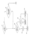
本実施形態にかかる光信号発生装置は、例えば光ファイバ通信システムにおける光送信器として用いられ、図1に示すように、シングルモードレーザ110と、位相調整器120と、光増幅器130と、強度変調器140と、反射鏡210と、波長フィルタ220とを備える。
そして、シングルモードレーザ110からの出力光は、位相調整器120、光増幅器130及び強度変調器140を通過した後、反射鏡210及び波長フィルタ220を透過し、光信号発生装置の出力光として出力されるようになっている。一方、シングルモードレーザ110からの出力光の一部は反射鏡210によって反射され、シングルモードレーザ110へ戻されるようになっている。The optical signal generator according to the present embodiment is used as an optical transmitter in an optical fiber communication system, for example, and as shown in FIG. 1, a
The output light from the
本実施形態では、図1に示すように、シングルモードレーザ110、位相調整器120、光増幅器130、強度変調器140は、この順番で同一基板(半導体基板;例えばn型InP基板)100上に形成され、光学的に接続されており、集積デバイス10を構成している。そして、この集積デバイス10の端面(出力光が出射される側の端面;ここでは強度変調器140の端面)に反射鏡210として反射膜が設けられている。
In this embodiment, as shown in FIG. 1, the
ここで、シングルモードレーザ110は、例えば通信用半導体レーザであり、ここでは分布帰還型(DFB:distributed feedback)レーザである。
反射鏡210は、例えば誘電体多層膜などの反射膜であり、シングルモードレーザ110からの出力光の一部を反射してシングルモードレーザ110へ戻す機能を有する。ここでは、反射鏡210の反射率は0.1%である。Here, the
The reflecting
この反射鏡210と、シングルモードレーザ110の出力光が出射される側とは反対側に設けられた反射鏡(図示せず)とによって、シングルモードレーザ110の共振器(レーザ共振器)20とは別の共振器21が構成される。このため、本光信号発生装置は、レーザ共振器20と、別の共振器21とからなる複合共振器を備えることになる。
位相調整器(位相制御器)120は、半導体位相変調器であり、量子井戸構造をコア層とする量子井戸導波路に、例えば電流を注入して屈折率を変化させて位相を調整する構造になっている。そして、この位相調整器120は、シングルモードレーザ110と反射鏡210との間に設けられている。つまり、別の共振器21の内部に位相調整器120が設けられている。A resonator (laser resonator) 20 of the
The phase adjuster (phase controller) 120 is a semiconductor phase modulator having a structure in which a phase is adjusted by, for example, injecting current into a quantum well waveguide having a quantum well structure as a core layer to change a refractive index. It has become. The
本実施形態では、位相調整器120は、強度変調器140による強度変調に応じて生じる信号オン状態と信号オフ状態との間の周波数差(周波数変調振幅)を調整するために用いられる。
光増幅器130は、例えば量子井戸導波路構造に例えば電流を注入して利得を発生させる半導体光増幅器(SOA)であり、シングルモードレーザ110と反射鏡210との間に設けられている。つまり、別の共振器21の内部に光増幅器130が設けられている。ここでは、光増幅器130の利得は5dBである。In the present embodiment, the
The
強度変調器140は、例えば量子井戸導波路構造に例えば電圧を印加して吸収係数を変化させて強度変調を行なう半導体電界吸収型変調器であって、シングルモードレーザ110と反射鏡210との間に設けられている。つまり、レーザ共振器20とは別の共振器21の内部に強度変調器140が設けられている。ここでは、強度変調器140の挿入損失は5dBである。つまり、強度変調器140は消光していない状態で5dBの損失を持っている。このように、本実施形態では、直接変調方式でなく、外部変調方式としているため、動的波長チャープが小さい。
The
このように構成されている光信号発生装置では、強度変調器140による強度変調に応じて生じる信号オン状態と信号オフ状態との間の周波数差(周波数変調振幅)は、位相に応じて変化することになる。このため、信号オン状態と信号オフ状態との間の周波数差(周波数変調振幅)は、位相調整器120によって調整できることになる。
波長フィルタ220は、例えば誘電体多層膜などからなる光帯域通過フィルタであって、反射鏡210を透過した光(光信号)が入射する位置(集積デバイス10からの出力光が光学的に結合する位置)に設けられている。In the optical signal generator configured as described above, the frequency difference (frequency modulation amplitude) between the signal ON state and the signal OFF state generated according to the intensity modulation by the
The
この波長フィルタ220は、強度変調器140による強度変調に応じて生じる周波数変調(周波数変調波形;周波数変調成分)を強度変調(強度変調波形)に変換する機能を有する。なお、波長フィルタ220に入力される光信号の強度変調成分(強度変調波形)は、波長フィルタ220による影響を受けず、波長フィルタ220の前後で変わらない。また、波長フィルタ220の透過帯域は、波長多重通信で用いられるチャンネルのいずれかに一致している。なお、ここでは、波長フィルタ220として、透過型のフィルタを用いているが、反射型のフィルタを用いても良い。
The
本実施形態にかかる光信号発生装置は、上述のように構成されるため、以下のように動作する。
つまり、本光信号発生装置では、図1に示すように、シングルモードレーザ110の出射光は、位相調整器120を通過し、光増幅器130によって増幅され、強度変調器140を通過して、反射鏡210に至る。反射鏡210は、その反射率に対応して光(光信号)をシングルモードレーザ110側へ反射する。反射光は、強度変調器140を通過し、光増幅器130によって増幅され、位相調整器120を通過して、シングルモードレーザ110に入射する。Since the optical signal generator according to the present embodiment is configured as described above, it operates as follows.
That is, in this optical signal generator, as shown in FIG. 1, the light emitted from the
このように構成することで、本光信号発生装置(集積デバイス)は、シングルモードレーザ110が持つレーザ共振器20とは別に、シングルモードレーザ110から反射鏡210までのもう1つの共振器21を持ち、これはシングルモードレーザ110とは別の共振周波数及びしきい値電流を持つこととなる。これらの2つの共振器20,21からなる複合共振器は、共振周波数の変化及びしきい値電流の変動による内部キャリア密度の変化によって、発振周波数が変動することになる。
With this configuration, the optical signal generation device (integrated device) includes another resonator 21 from the
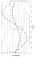
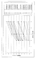
つまり、図2に示すように、複合共振器(集積デバイス10)の発振周波数は、位相に応じて変動することになる。なお、図2中、実線Aは信号オン状態(変調器による消光なし)の周波数変動を示しており、実線Bは信号オフ状態(変調器によって消光なしの場合に対して5dB消光)の周波数変動を示している。また、図2では、シングルモードレーザ110の発振周波数(周波数変動0GHz)に対してどのくらい発振周波数が変動したかを示しており、周波数変動の値(GHz)は、周波数が高くなった場合をプラスの値とし、周波数が低くなった場合をマイナスの値としている。
That is, as shown in FIG. 2, the oscillation frequency of the composite resonator (integrated device 10) fluctuates according to the phase. In FIG. 2, the solid line A indicates the frequency fluctuation in the signal ON state (no extinction by the modulator), and the solid line B indicates the frequency fluctuation in the signal OFF state (5 dB extinction in the case of no extinction by the modulator). Is shown. Further, FIG. 2 shows how much the oscillation frequency fluctuates with respect to the oscillation frequency of the single mode laser 110 (
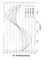
つまり、強度変調器140に印加する信号を変化させ、強度変調器140によって強度変調を行なうと、シングルモードレーザ110に戻る光の位相と強度が変化し、これによって、信号オン状態と信号オフ状態とで発振周波数が変化する。つまり、周波数変調が行なわれる。また、図2に示すように、信号オン状態の発振周波数と信号オフ状態の発振周波数は、それぞれ、位相に応じて変化する。そして、信号オン状態と信号オフ状態とで、位相変化に対する発振周波数の変動幅が異なるため、図3に示すように、信号オン状態と信号オフ状態との間の発振周波数差(周波数変調振幅)は位相に応じて変動することになる。また、図3に示すように、位相変化に対する周波数変調振幅の大きさの変化は、強度変調器140による消光比に応じて異なる。このため、位相調整器120及び強度変調器140の制御を適切に行なうことで、所望の周波数変調振幅が得られることになる。なお、図3中、縦軸の周波数変調振幅の値(GHz)は、信号オン状態の周波数から信号オフ状態の周波数を引いた値である。
That is, when the signal applied to the
したがって、反射鏡210を透過した光(光信号)は周波数変調成分(周波数変調光)を含み、この周波数変調光は、波長フィルタ220を透過する際に、波長フィルタ220によって強度変調光に変換され、本光信号発生装置の出力光として出力される。
さらに詳述すると、まず、図3に示すように、位相を0から0.5π程度までの範囲でずらす場合、周波数変調振幅の値がマイナスであり、信号オン状態の周波数よりも信号オフ状態の周波数の方が高くなっている。一方、位相を0.5π程度からπ程度までの範囲でずらす場合、周波数変調振幅の値がプラスであり、信号オン状態の周波数よりも信号オフ状態の周波数の方が低くなっている。Therefore, the light (optical signal) transmitted through the reflecting
More specifically, as shown in FIG. 3, when the phase is shifted in the range of about 0 to 0.5π, the value of the frequency modulation amplitude is negative, and the signal off state is higher than the frequency in the signal on state. The frequency is higher. On the other hand, when the phase is shifted in a range from about 0.5π to about π, the value of the frequency modulation amplitude is positive, and the frequency in the signal off state is lower than the frequency in the signal on state.
また、波長フィルタ220の透過特性は、図5(A),図5(B)に示すように、周波数に対して山型の特性になっている。また、波長フィルタ220の透過特性のスロープ中央付近に、シングルモードレーザ110の発振周波数が合わされている。
このため、位相を0から0.5π程度までの範囲でずらす場合は、図5(B)に示すように、信号オン状態の場合に波長フィルタ220に入力される光の波長よりも、信号オフ状態の場合に波長フィルタ220に入力される光の波長の方が、波長フィルタ220をより多く透過することになる。この場合、強度変調器140によって生成され、波長フィルタ220に入力される強度変調波形[入力波形;図5(B)中、点線で示す]に波長フィルタ220によって変換されて生成される強度変調波形が重ね合わされ、互いに弱めあい、これが出力される強度変調波形[出力波形;図5(B)中、実線で示す]となるため、あまり大きな出力消光比が得られない。Further, the transmission characteristic of the
Therefore, when the phase is shifted in the range of about 0 to 0.5π, as shown in FIG. 5 (B), the signal is turned off rather than the wavelength of the light input to the
一方、位相を0.5π程度からπ程度までの範囲でずらす場合は、図5(A)に示すように、信号オフ状態の場合に波長フィルタ220に入力される光の波長よりも、信号オン状態の場合に波長フィルタ220に入力される光の波長の方が、波長フィルタ220をより多く透過することになる。この場合、強度変調器140によって生成され、波長フィルタ220に入力される強度変調波形[入力波形;図5(A)中、点線で示す]に波長フィルタ220によって変換されて生成される強度変調波形が重ね合わされ、互いに強めあい、これが出力される強度変調波形[出力波形;図5(A)中、実線で示す]となるため、大きな出力消光比が得られる。
On the other hand, when the phase is shifted in a range from about 0.5π to about π, as shown in FIG. 5 (A), the signal is turned on rather than the wavelength of the light input to the
ここで、図4は、波長フィルタ220を透過した後の光信号の消光比(波長フィルタ220を介して出力される光信号の消光比;出力消光比)と、強度変調器140による消光比及び位相との関係を示している。
図4に示すように、位相を0.5π程度からπ程度までの範囲でずらす場合は、強度変調器140による消光比に、波長フィルタ220によって得られる消光比が加えられたものが出力消光比となるため、強度変調器140による消光比が小さい場合であっても、所望の出力消光比が得られることになる。特に、波長フィルタ220に入力される周波数変調信号の振幅(周波数変調振幅)は位相に応じて変化するため(図3参照)、図4に示すように、波長フィルタ220を介して出力される強度変調信号の振幅(即ち、出力消光比)も位相に応じて変化する。また、図4に示すように、位相変化に対する出力消光比の変化は、強度変調器140による消光比に応じて異なる。このため、位相調整器120及び強度変調器140の制御を適切に行なうことで、出力消光比を調整することができ、所望の出力消光比が得られることになる。Here, FIG. 4 shows the extinction ratio of the optical signal after passing through the wavelength filter 220 (the extinction ratio of the optical signal output through the
As shown in FIG. 4, when the phase is shifted in the range from about 0.5π to about π, the output extinction ratio is obtained by adding the extinction ratio obtained by the
このように、シングルモードレーザ110の発振周波数と波長フィルタ220の動作波長(ここでは波長フィルタ220の透過特性のスロープ中央付近の周波数)を合わせた状態で、位相調整器120及び強度変調器140を制御することで、所望の周波数変調振幅及び所望の消光比が得られることになる。
ところで、本光信号発生装置は、各構成要素110,120,130,140を制御するための制御回路(コントローラ)400を備える。Thus, in a state where the oscillation frequency of the
By the way, this optical signal generator includes a control circuit (controller) 400 for controlling each of the
特に、本実施形態では、制御回路400は、強度変調器140による強度変調に応じて生じる信号オン状態と信号オフ状態との間の周波数差(周波数変調振幅)が、所望の周波数差(周波数変調振幅)になるように位相調整器120を制御するように構成されている。
ここでは、制御回路400は、強度変調器140による強度変調に応じて生じる信号オン状態と信号オフ状態との間の周波数差(周波数変調振幅)が、ビットレートに応じた周波数差になるように位相調整器120を制御するように構成されている。例えば、信号品質を保つために、強度変調器140による強度変調に応じて生じる信号オン状態と信号オフ状態との間の周波数差(周波数変調振幅)(GHz)は、ビットレート(Gbps)の値の半分の値にするのが好ましい。In particular, in the present embodiment, the
Here, the
また、制御回路400は、波長フィルタ220を介して出力される光の消光比(出力消光比)が所望の値になるように位相調整器120を制御するように構成されている。
具体的には、制御回路400は、図6のフローチャートに示すような制御(光信号発生装置の制御方法;駆動方法)を行なう。
まず、制御回路400は、シングルモードレーザ110に一定電流を供給して動作させた状態で、シングルモードレーザ110の発振波長(発振周波数)と波長フィルタ220の動作波長(動作周波数)とを合わせる制御(第1の制御)を行なう(図6中、ステップS10〜S30)。Further, the
Specifically, the
First, the
ここでは、制御回路400は、シングルモードレーザ110を一定電流条件で駆動(起動)し、強度変調器140を消光比1dB,ビットレート10Gbpsで駆動(起動)し、光増幅器130を駆動(起動)する(ステップS10)。そして、制御回路400は、集積デバイス10の温度(素子駆動温度)を制御する(ステップS20、S30)。具体的には、制御回路400は、シングルモードレーザ110の発振波長(発振周波数)と波長フィルタ220の動作波長(動作周波数)とが等しいか否かを判定し(ステップS20)、この結果、等しい場合(YESルート)は、後述の第2の制御(ステップS40〜S70)へ進み、等しくない場合(NOルート)は、温度を再設定して、集積デバイス10の温度を制御する(ステップS30)。
Here, the
次に、制御回路400は、強度変調器140を矩形波電気信号(変調信号)で駆動して強度変調を与えた状態で、位相調整器120を駆動して、波長フィルタ220を透過した後の光信号の消光比(出力消光比)が最大となるように位相調整器120を制御する(第2の制御;ステップS40〜S70)。本実施形態では、図4中、0.7π付近に位相を調整する。
Next, the
この第2の制御を行なうことによって、大きな出力消光比が得られる領域(図4中、右側の高い山)において(本実施形態では位相シフト量0.5π程度からπ程度までの範囲で)、所望の周波数変調振幅や所望の消光比にするための制御を行なえるようにしている。
これは、強度変調器140による強度変調によって信号オン状態とした場合の出力光波長の波長フィルタ220の透過率(フィルタ透過率)が、信号オフ状態とした場合の出力光波長のフィルタ透過率よりも高くなるように位相を調整することを意味する。つまり、強度変調器140による強度変調によって信号オン状態から信号オフ状態へと変化するときに、出力光の波長が波長フィルタ220の透過特性において透過率が高い波長から低い波長へと変化する一方、強度変調器140による強度変調によって信号オフ状態から信号オン状態へと変化するときに、出力光の波長が波長フィルタ220の透過特性において透過率が低い波長から高い波長へと変化するように位相を調整することを意味する(即ち、強度変調器140による強度変調によって得られる信号オン状態及び信号オフ状態と、波長フィルタ220を透過する光の信号オン状態と信号オフ状態とを一致させるように位相を調整することを意味する)。By performing this second control, in a region where a large output extinction ratio can be obtained (high peak on the right side in FIG. 4) (in this embodiment, in the range from about 0.5π to about π in phase shift amount), Control to obtain a desired frequency modulation amplitude and a desired extinction ratio can be performed.
This is because the transmittance (filter transmittance) of the
なお、第2の制御は、これに限られるものではなく、制御回路400は、周波数変調振幅が所望の符号で絶対値が最大となるように位相調整器120を制御するようにしても良い。本実施形態では、周波数変調振幅の値を、信号オン状態の周波数から信号オフ状態の周波数を引いた周波数差としているため、所望の符号はプラスである。このため、図3中、0.7π付近に位相を調整することになる。
Note that the second control is not limited to this, and the
具体的には、制御回路400は、まず、初期設定が済んでいるかどうかを判定し(ステップS40)、初期設定が済んでいる場合(YESルート)は、後述の第3の制御(ステップS80〜S110)へ進み、初期設定が済んでいない場合(NOルート)は、ステップS50へ進み、波長フィルタ220を透過した後の光信号の消光比(出力消光比)が最大であるか否かを判定する。この結果、出力消光比が最大であると判定した場合(YESルート)は、初期設定を終了して(ステップS70)、後述の第3の制御(ステップS80〜S110)へ進み、出力消光比が最大でないと判定した場合(NOルート)は、位相調整器120を制御して位相を調整する(ステップS60)。
Specifically, the
本実施形態では、第2の制御は、初期設定時(装置立ち上げ時)のみ行なうこととし、繰り返し行なわないようにするために、出力消光比が最大であると判定されたら、初期設定終了フラグを立てるようにしている。そして、初期設定終了フラグが立っているか否かによって初期設定が済んでいるか否かを判定するようにしている。
次に、制御回路400は、周波数差(周波数変調振幅)が所望の値(例えば5GHz)でなく、かつ、周波数差が極大でない場合に、周波数差が所望の値(例えば5GHz)となるように位相調整器120を制御する一方、周波数差が極大である場合に、消光比が大きくなるように強度変調器140を制御する(第3の制御;ステップS80〜S110)。In the present embodiment, the second control is performed only at the time of initial setting (at the time of starting up the apparatus), and when it is determined that the output extinction ratio is maximum so as not to be repeatedly performed, the initial setting end flag is set. To stand up. Then, it is determined whether or not the initial setting is completed depending on whether or not the initial setting end flag is set.
Next, the
具体的には、制御回路400は、周波数差が所望の値(例えば5GHz)と等しいか否かを判定する(ステップS80)。この判定の結果、周波数差が所望の値(例えば5GHz)と等しくない場合(NOルート)は、さらに、周波数差(Δf)が極大であるか否かを判定する(ステップS90)。
そして、周波数差が所望の値(例えば5GHz)よりも大きく、周波数差が極大でない場合は、位相調整器120を制御して位相を調整して周波数差を減少させる(ステップS100)。また、周波数差が所望の値(例えば5GHz)よりも小さく、周波数差が極大でない場合は、位相調整器120を制御して位相を調整して周波数差を増加させる(ステップS100)。また、周波数差が所望の値(例えば5GHz)と等しくなく、周波数差が極大である場合は、強度変調器140に供給される変調信号の振幅電圧を増加させて消光比を大きくする(ステップS110)。Specifically, the
If the frequency difference is larger than a desired value (for example, 5 GHz) and the frequency difference is not maximal, the
ここでは、周波数差(Δf)が極大であるか否かを判定するために、以下のような制御を行なう。
つまり、制御回路400は、例えば図7に示すように、位相調整器120を制御して位相を調整した場合に、Δfが所望のΔfに近づかなかった場合、逆方向に制御する一方、Δfが所望のΔfに近づいた場合、同方向に制御する。そして、過去2回同方向に制御した場合に、2回目でΔfが所望のΔfに近づかなかったら、その2つのステップの間に極大が含まれていることになるので、制御を弱めて逆方向に制御する。Here, in order to determine whether or not the frequency difference (Δf) is maximal, the following control is performed.
That is, for example, as shown in FIG. 7, when the phase is adjusted by controlling the
このような制御は、図8のフローチャートに示すような手順で行なわれる。なお、図8のフローチャートに示す処理は、図6のステップS90で行なわれる処理である。
つまり、まず、Δfの変化幅が所定の値以下であるか否かを判定し(ステップA10)、Δfの変化幅が所定の値以下である場合(YESルート)は、さらに、所望のΔfと現在のΔfとの差の絶対値が所定の値以上であるか否かを判定する(ステップA20)。この判定の結果、所望のΔfと現在のΔfとの差の絶対値が所定の値以上であると判定した場合(YESルート)は、Δfは極大であると判定する。Such control is performed according to the procedure shown in the flowchart of FIG. The process shown in the flowchart of FIG. 8 is the process performed in step S90 of FIG.
That is, first, it is determined whether or not the change width of Δf is equal to or less than a predetermined value (step A10). If the change width of Δf is equal to or less than a predetermined value (YES route), the desired Δf is further determined. It is determined whether or not the absolute value of the difference from the current Δf is greater than or equal to a predetermined value (step A20). As a result of this determination, if it is determined that the absolute value of the difference between the desired Δf and the current Δf is greater than or equal to a predetermined value (YES route), it is determined that Δf is maximal.
一方、ステップA10でΔfの変化幅が所定の値よりも大きいと判定した場合(NOルート)、あるいは、ステップA20で所望のΔfと現在のΔfとの差の絶対値が所定の値よりも小さいと判定した場合(NOルート)は、さらに、所望のΔfに近づいたか否かを判定する(ステップA30)。
そして、所望のΔfに近づいたと判定した場合(YESルート)は、フラグをセットし(ステップA35)、位相調整器120を制御して位相を調整する(ステップA40)。一方、所望のΔfに近づいていないと判定した場合(NOルート)は、フラグがセットされているか否かを判定し(ステップA50)、フラグがセットされている場合は、制御強度を減少させ(ステップA60)、さらに、制御方向を逆転させ(ステップA70)、位相調整器120を制御して位相を調整する(ステップA40)。一方、ステップA50でフラグがセットされていないと判定した場合(NOルート)は、ステップA70へ進み、制御方向を逆転させ(ステップA70)、位相調整器120を制御して位相を調整する(ステップA40)。なお、ここでは位相を調整するステップ(位相制御ステップ)を「ステップA40」としているが、これは図6の「ステップS100」に相当する。On the other hand, when it is determined in step A10 that the change width of Δf is larger than the predetermined value (NO route), or in step A20, the absolute value of the difference between the desired Δf and the current Δf is smaller than the predetermined value. (NO route), it is further determined whether or not the desired Δf has been approached (step A30).
If it is determined that the desired Δf has been approached (YES route), a flag is set (step A35), and the phase is adjusted by controlling the phase adjuster 120 (step A40). On the other hand, if it is determined that the desired Δf is not approached (NO route), it is determined whether or not a flag is set (step A50). If the flag is set, the control intensity is decreased ( Further, the control direction is reversed (step A70), and the
次に、図6に示すように、制御回路400は、周波数差が所望の値(例えば5GHz)である場合に、波長フィルタ220を介して出力される光信号の消光比が所望の値(例えば10dB)以上になるように強度変調器140を制御する(第4の制御;ステップS110、S120)。
具体的には、制御回路400は、ステップS80で、周波数差が所望の値(例えば5GHz)と等しいと判定した場合(YESルート)に、ステップS120へ進み、波長フィルタ220を透過した後の光信号の消光比(出力消光比)が所望の値(例えば10dB)以上であるか否かを判定する。Next, as shown in FIG. 6, when the frequency difference is a desired value (for example, 5 GHz), the
Specifically, when the
この結果、出力消光比が所望の値(例えば10dB)よりも小さいと判定した場合(NOルート)は、ステップS110へ進み、強度変調器140に供給される変調信号の振幅電圧(変調器駆動振幅電圧)を増加させる。つまり、周波数差が所望の値(例えば5GHz)と等しく、かつ、波長フィルタ220を透過した後の光信号の消光比が所望の値(例えば10dB)よりも小さい場合、強度変調器140に供給される変調信号の振幅電圧(変調器駆動振幅電圧)を増加させる。
As a result, when it is determined that the output extinction ratio is smaller than a desired value (for example, 10 dB) (NO route), the process proceeds to step S110 and the amplitude voltage (modulator drive amplitude) of the modulation signal supplied to the
一方、出力消光比が所望の値(例えば10dB)以上であると判定した場合(YESルート)は、起動完了フラグをセットし(ステップS130)、ステップS20へ戻り、上述の第1、第3、第4の制御を繰り返し行なう。これにより、周波数差(周波数変調振幅)が所望の値(例えば5GHz)と等しく、かつ、出力消光比が所望の値(例えば10dB)以上の光信号が、波長フィルタ220を介して出力されることになる。
On the other hand, when it is determined that the output extinction ratio is equal to or higher than a desired value (for example, 10 dB) (YES route), the start completion flag is set (step S130), the process returns to step S20, and the above-described first, third, The fourth control is repeated. Thereby, an optical signal having a frequency difference (frequency modulation amplitude) equal to a desired value (for example, 5 GHz) and an output extinction ratio equal to or greater than a desired value (for example, 10 dB) is output through the
したがって、本実施形態にかかる光信号発生装置及びその調整方法によれば、動的波長チャープが小さく、簡易、かつ、実用的な構成で、強度変調とは独立に、強度変調による信号オン状態と信号オフ状態との間の周波数差(周波数変調振幅)を調整できるため、波形劣化を抑制して伝送距離を伸ばすことができ、異なる変調ビットレートにも対応できるという利点がある。 Therefore, according to the optical signal generation device and the adjustment method thereof according to the present embodiment, the dynamic wavelength chirp is small, the configuration is simple and practical, and the signal on state by the intensity modulation is independent of the intensity modulation. Since the frequency difference (frequency modulation amplitude) from the signal off state can be adjusted, there is an advantage that the waveform distance can be suppressed and the transmission distance can be extended, and different modulation bit rates can be accommodated.
つまり、周波数変調量(周波数差;周波数変調振幅)と強度変調量(消光比)を任意に設定でき、かつ、動的波長チャープが小さいため、波長フィルタ透過後の光信号として、異なる変調ビットレートに対しても伝送距離が伸びる光信号を、簡易な構成で得ることができるという利点がある。
[第2実施形態]
次に、第2実施形態にかかる光信号発生装置及びその調整方法について、図9〜図11を参照しながら説明する。In other words, the frequency modulation amount (frequency difference; frequency modulation amplitude) and intensity modulation amount (extinction ratio) can be set arbitrarily, and the dynamic wavelength chirp is small, so that different modulation bit rates can be used as optical signals after passing through the wavelength filter. However, there is an advantage that an optical signal having a long transmission distance can be obtained with a simple configuration.
[Second Embodiment]
Next, an optical signal generation device and an adjustment method thereof according to the second embodiment will be described with reference to FIGS.
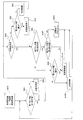
本実施形態にかかる光信号発生装置は、上述の第1実施形態のものに対し、図9に示すように、駆動回路410,420,430,440、及び、モニタ回路300,301を備える点が異なる。なお、図9では、上述の第1実施形態のもの(図1参照)と同一のものには同一の符号を付している。
本光信号発生装置は、上述の第1実施形態の構成に加え、図9に示すように、第1ビームスプリッタ310と、第1モニタPD(フォトディテクタ;フォトダイオード)320と、モニタ用波長フィルタ330と、第2モニタPD(フォトディテクタ;フォトダイオード)340と、第2ビームスプリッタ350と、第3モニタPD(フォトディテクタ;フォトダイオード)360と、シングルモードレーザ110を駆動するレーザ用駆動回路410と、位相調整器120を駆動する位相調整器用駆動回路420と、光増幅器130を駆動する光増幅器用駆動回路430と、強度変調器140を駆動する強度変調器用駆動回路440と、集積デバイス(素子全体)10の温度を制御するペルチェコントローラ(ペルチェ素子)450とを備える。The optical signal generator according to the present embodiment is different from that of the first embodiment described above in that
In addition to the configuration of the first embodiment described above, the present optical signal generator includes a
ここで、第1ビームスプリッタ310は、例えばウェッジ角の入った石英板である。
モニタ用波長フィルタ330は、例えば、第1ビームスプリッタ310の出射側端面に積層された誘電体多層膜である。このモニタ用波長フィルタ330は、図11に示すような透過特性を有し、波長に対して線形に変化する部分を有する。なお、ここでは、モニタ用波長フィルタ330として、透過型のフィルタを用いているが、反射型のフィルタを用いても良い。Here, the
The
第2ビームスプリッタ350は、例えば石英板である。
ここでは、第1ビームスプリッタ310は、集積デバイス10の信号出力側(波長フィルタ220が設けられている側)と反対側に配置されている。また、第1ビームスプリッタ310の一方の出力側に第1モニタPD320が配置されている。さらに、第1ビームスプリッタ310の他方の出力側にモニタ用波長フィルタ330及び第2モニタPD340が配置されている。The
Here, the
そして、第1ビームスプリッタ310によって分岐された出力光の一部を第1モニタPD320によって検出し、第1ビームスプリッタ310によって分岐された出力光の一部のうちモニタ用波長フィルタ330を透過した光を第2モニタPD340によって検出するようになっている。つまり、第1モニタPD320によって、シングルモードレーザ110からの出力光(ここでは波長フィルタ220が設けられている信号出力側と反対側に出力される光)の一部を受光するようになっている。また、シングルモードレーザ110からの出力光(ここでは波長フィルタ220が設けられている信号出力側と反対側に出力される光)の一部はモニタ用波長フィルタ330を透過し、第2モニタPD340によって、モニタ用波長フィルタ330を透過した光を受光するようになっている。
Then, a part of the output light branched by the
また、第2ビームスプリッタ350は、集積デバイス10の信号出力側に設けられた波長フィルタ220の出力側に配置されている。また、第2ビームスプリッタ350によって分岐された光が出力される側に第3モニタPD360が配置されている。そして、第2ビームスプリッタ350によって分岐された出力光の一部を第3モニタPD360によって検出するようになっている。つまり、第3モニタPD360によって、波長フィルタ220を透過した光信号の一部を受光するようになっている。
The
そして、本実施形態では、制御回路400は、第1モニタPD320、第2モニタPD340及び第3モニタPD360からの信号に基づいて、各駆動回路(ドライブ回路)410,420,430,440を介して、シングルモードレーザ110、位相調整器120、光増幅器130、強度変調器140及び集積デバイス10の温度を制御するように構成されている。
In the present embodiment, the
ここでは、第1モニタPD320、第2モニタPD340及び第3モニタPD360からの検出信号は制御回路400に入力され、制御回路400からの制御信号は、各駆動回路410,420,430,440へ出力され、各駆動回路410,420,430,440からの駆動信号がシングルモードレーザ110、位相調整器120、光増幅器130、強度変調器140及びペルチェコントローラ(波長調整手段)450へ出力されるようになっている。
Here, the detection signals from the
まず、上述の第1実施形態において制御回路400によって行なわれる第1の制御[即ち、シングルモードレーザ110の発振波長(発振周波数)と波長フィルタ220の動作波長(動作周波数)とを合わせる制御]は、第1モニタPD320及び第2モニタPD340からの信号から得られる波長情報に基づいてペルチェコントローラ450を制御することによって行なうようになっている。つまり、制御回路400は、第1モニタPD320及び第2モニタPD340からの信号に基づいて、図11に示すように、モニタ用波長フィルタ330の透過特性のスロープ中央部分に、シングルモードレーザ110の発振波長を合わせるようにしている。これにより、シングルモードレーザ110の発振波長(発振周波数)と波長フィルタ220の動作波長(動作周波数)とが合わされることになる。
First, the first control performed by the
次に、上述の第1実施形態において制御回路400によって行なわれる第2の制御[即ち、波長フィルタ220を透過した後の光信号の出力消光比が最大となるようにするための制御]は、第3モニタPD360からの信号に基づいて位相調整器120を制御することによって行なうようになっている。
次に、上述の第1実施形態において制御回路400によって行なわれる第3の制御[即ち、周波数差(周波数変調振幅)が所望の値(例えば5GHz)でなく、かつ、極大でない場合に、周波数差が所望の値(例えば5GHz)となるようにし、周波数差が極大である場合に、消光比が大きくなるようにする制御]は、第1モニタPD320及び第2モニタPD340からの信号に基づいて位相調整器120又は強度変調器140を制御することによって行なうようになっている。Next, the second control performed by the
Next, the third control performed by the
次に、上述の第1実施形態において制御回路400によって行なわれる第4の制御[即ち、周波数差が所望の値(例えば5GHz)である場合に、波長フィルタ220を介して出力される光信号の消光比が所望の値(例えば10dB)以上になるようにする制御]は、第3モニタPD360からの信号に基づいて強度変調器140を制御することによって行なうようになっている。
Next, the fourth control performed by the
具体的には、制御回路400は、図10のフローチャートに示すような制御(光信号発生装置の制御方法;駆動方法)を行なう。
まず、制御回路400は、シングルモードレーザ110に一定電流を供給して動作させた状態で、シングルモードレーザ110の発振波長(発振周波数)と波長フィルタ220の動作波長(動作周波数)とを合わせる制御(第1の制御)を行なう(図10中、ステップB10〜B30)。Specifically, the
First, the
本実施形態では、制御回路400は、シングルモードレーザ110を一定電流条件で駆動(起動)し、強度変調器140を消光比1dB,ビットレート10Gbpsで駆動(起動)し、光増幅器130を駆動(起動)する(ステップB10)。そして、制御回路400は、第2モニタPD340からの信号(直流成分;平均周波数)と第1モニタPD320からの信号(直流成分;平均周波数)との比[第2モニタPD340からの信号(直流成分)/第1モニタPD320からの信号(直流成分)]の値(第1モニタ値)が第1設定値と等しいか否かを判定する(ステップB20)。なお、第1設定値は、シングルモードレーザ110の発振波長が波長フィルタ220の動作波長と合っているときの第1モニタ値である。
In the present embodiment, the
この結果、等しくない場合(NOルート)は、温度を再設定して、ペルチェコントローラ450を制御して集積デバイス10の温度(素子駆動温度)を制御し(ステップB30)、等しい場合(YESルート)は、後述の第2の制御(ステップB40〜B70)へ進む。
次に、制御回路400は、波長フィルタ220を透過した後の光信号の出力消光比が最大となるように位相調整器120を制御する(第2の制御;ステップB40〜B70)。As a result, if they are not equal (NO route), the temperature is reset and the
Next, the
本実施形態では、制御回路400は、まず、初期設定が済んでいるかどうかを判定し(ステップB40)、初期設定が済んでいない場合(NOルート)は、ステップB50へ進み、第3モニタPD360からの信号(交流成分;強度変動幅)と第3モニタPD360からの信号(直流成分;平均強度)との比[第3モニタPD360からの信号(交流成分)/第3モニタPDからの信号(直流成分)]の値(第3モニタ値;規格化した出力消光比の値)が最大であるか否かを判定する。この結果、最大でない場合(NOルート)は、位相調整器120を制御して位相を調整し(ステップB60)、最大である場合(YESルート)は、初期設定を終了して(ステップB70)、後述の第3の制御(ステップB80〜B110)へ進む。
In the present embodiment, the
次に、制御回路400は、周波数差(周波数変調振幅)が所望の値(例えば5GHz)でなく、かつ、周波数差が極大でない場合に、周波数差が所望の値(例えば5GHz)となるように位相調整器120を制御する一方、周波数差が極大である場合に、消光比が大きくなるように強度変調器140を制御する(第3の制御;ステップB80〜B110)。
Next, the
本実施形態では、制御回路400は、第2モニタPD340からの信号(交流成分;周波数変動幅)と第1モニタPDからの信号(直流成分;平均周波数)との比[第2モニタPD340からの信号(交流成分)/第1モニタPD320からの信号(直流成分)]の値(第2モニタ値;規格化した周波数変調振幅の値)が第2設定値と等しいか否かを判定する(ステップB80)。なお、第2設定値は、周波数変調振幅が所望の値(例えば5GHz)と等しいときの第2モニタ値である。
In the present embodiment, the
この判定の結果、第2モニタ値が第2設定値と等しくない場合(NOルート)は、さらに、第2モニタ値が極大であるか否かを判定する(ステップB90)。そして、第2モニタ値が第2設定値と等しくなく、第2モニタ値が極大でない場合(NOルート)は、位相調整器120を制御して位相調整を行なって周波数変調振幅を調整する(ステップB100)。また、第2モニタ値が第2設定値と等しくなく、第2モニタ値が極大である場合(YESルート)は、強度変調器140に供給される変調信号の振幅を増大させる制御を行なって消光比を大きくする(ステップB110)。
If the result of this determination is that the second monitor value is not equal to the second set value (NO route), it is further determined whether or not the second monitor value is maximal (step B90). If the second monitor value is not equal to the second set value and the second monitor value is not maximal (NO route), the
次に、制御回路400は、周波数差が所望の値(例えば5GHz)である場合に、波長フィルタ220を介して出力される光信号の消光比が所望の値(例えば10dB)以上になるように強度変調器140を制御する(第4の制御;ステップB110、B120)。
本実施形態では、制御回路400は、ステップB80で、第2モニタ値が第2設定値と等しいと判定した場合(YESルート)に、ステップB120へ進み、第3モニタPD360からの信号(交流成分)と第3モニタPD360からの信号(直流成分)との比[第3モニタPD360からの信号(交流成分)/第3モニタPD360からの信号(直流成分)]の値(第3モニタ値)が第3設定値以上であるか否かを判定する。なお、第3設定値は、出力消光比が所望の値(例えば10dB)と等しいときの第3モニタ値である。Next, when the frequency difference is a desired value (for example, 5 GHz), the
In the present embodiment, if the
この結果、第3モニタ値が第3設定値よりも小さいと判定した場合(NOルート)は、ステップB110へ進み、強度変調器140に供給される変調信号の振幅電圧(変調器駆動振幅電圧)を増大させる制御を行なって、波長フィルタ220を透過した後の光信号の消光比(出力消光比)を大きくする。
一方、第3モニタ値が第3設定値以上であると判定した場合(YESルート)は、起動完了フラグをセットし(ステップB130)、ステップB20へ戻り、上述の第1、第3、第4の制御を繰り返し行なう。これにより、周波数差(周波数変調振幅)が所望の値(例えば5GHz)と等しく、かつ、出力消光比が所望の値(例えば10dB)以上の光信号が、波長フィルタ220を介して出力されることになる。As a result, when it is determined that the third monitor value is smaller than the third set value (NO route), the process proceeds to Step B110 and the amplitude voltage of the modulation signal supplied to the intensity modulator 140 (modulator drive amplitude voltage). To increase the extinction ratio (output extinction ratio) of the optical signal after passing through the
On the other hand, if it is determined that the third monitor value is greater than or equal to the third set value (YES route), the activation completion flag is set (step B130), the process returns to step B20, and the first, third, and fourth described above are performed. Repeat the above control. Thereby, an optical signal having a frequency difference (frequency modulation amplitude) equal to a desired value (for example, 5 GHz) and an output extinction ratio equal to or greater than a desired value (for example, 10 dB) is output through the
なお、その他の詳細は、上述の第1実施形態及びその変形例のものと同じであるため、ここではその説明を省略する。
したがって、本実施形態にかかる光信号発生装置及びその調整方法によれば、上述の第1実施形態の場合と同様に、動的波長チャープが小さく、簡易、かつ、実用的な構成で、強度変調とは独立に、強度変調による信号オン状態と信号オフ状態との間の周波数差(周波数変調振幅)を調整できるため、波形劣化を抑制して伝送距離を伸ばすことができ、異なる変調ビットレートにも対応できるという利点がある。Since other details are the same as those of the first embodiment and its modification, the description thereof is omitted here.
Therefore, according to the optical signal generation device and the adjustment method thereof according to the present embodiment, as in the case of the first embodiment described above, the dynamic wavelength chirp is small, and the intensity modulation is performed with a simple and practical configuration. Independently of frequency modulation, the frequency difference between the signal on state and the signal off state (frequency modulation amplitude) due to intensity modulation can be adjusted, so that the waveform can be suppressed and the transmission distance can be extended, so that different modulation bit rates can be achieved. Has the advantage of being able to handle.
つまり、周波数変調量(周波数差;周波数変調振幅)と強度変調量(消光比)を任意に設定でき、かつ、動的波長チャープが小さいため、波長フィルタ透過後の光信号として、異なる変調ビットレートに対しても伝送距離が伸びる光信号を、簡易な構成で得ることができるという利点がある。
[第3実施形態]
次に、第3実施形態にかかる光信号発生装置及びその調整方法について、図12〜図16を参照しながら説明する。In other words, the frequency modulation amount (frequency difference; frequency modulation amplitude) and intensity modulation amount (extinction ratio) can be set arbitrarily, and the dynamic wavelength chirp is small, so that different modulation bit rates can be used as optical signals after passing through the wavelength filter. However, there is an advantage that an optical signal having a long transmission distance can be obtained with a simple configuration.
[Third Embodiment]
Next, an optical signal generation device and an adjustment method thereof according to the third embodiment will be described with reference to FIGS.
本実施形態にかかる光信号発生装置は、上述の第2実施形態のものに対し、上述の第2実施形態における第2の制御[波長フィルタ220を介して出力される光信号の出力消光比が最大となるようにする制御]を、ディザ信号に基づいて行なうようになっている点が異なる(図16参照)。
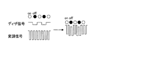
本実施形態では、図12に示すように、制御回路400は、強度変調器140に変調信号のビットレートよりも十分に遅い低周波のディザ信号を供給し、ディザ信号に基づいて、波長フィルタ220を介して出力される光(光信号)の出力消光比が最大となるように位相調整器120を制御するように構成されている。なお、図12では、上述の第2実施形態のもの(図9参照)と同一のものには同一の符号を付している。The optical signal generator according to the present embodiment is different from that of the second embodiment described above in the second control in the second embodiment described above [the output extinction ratio of the optical signal output via the
In this embodiment, as shown in FIG. 12, the
なお、本実施形態では、集積デバイス10は光増幅器130を備えないものとし、位相調整器120と強度変調器140の配置を変えている。また、説明の便宜上、基板100、反射鏡210、駆動回路410、420は省略している。さらに、モニタ用波長フィルタ330としては図15に示すような透過特性を有するエタロンフィルタを用いる。
そして、制御回路400が駆動回路440を介して強度変調器140を駆動する場合に、制御回路400からの制御信号に基づいて、駆動回路440が、図13に示すように低周波のディザ信号を重畳した変調信号を、強度変調器140に供給するようになっている。ここでは、ディザ信号の周波数は5kHzとしている。In the present embodiment, the
When the
なお、ここでは、ディザ信号を5kHzにしているが、これに限られるものではなく、より高速であっても、より低速であってもよい。ただし、第1,第2モニタPD320,340からの出力を直流成分と交流成分とに分ける際の遮断周波数以下の周波数とするのが望ましい。
また、制御回路400は、ディザ信号に基づく位相調整器120の制御を完了した後、強度変調器140に対するディザ信号の供給を停止する制御を行なうように構成されている。Here, the dither signal is set to 5 kHz. However, the dither signal is not limited to this, and may be faster or slower. However, it is desirable to set the output from the first and
Further, the
ところで、本実施形態では、上述の第2実施形態における第2の制御を、ディザ信号に基づいて行なうようにしているが、これは以下の理由による。
変調信号のオン/オフによって、反射率が高い状態/低い状態となり、シングルモードレーザ110への戻り光量が変調されるのと同様に、ディザ信号のオン/オフによって、反射率が高い状態/低い状態となり、シングルモードレーザ110への戻り光量が変調される。By the way, in the present embodiment, the second control in the second embodiment described above is performed based on the dither signal, for the following reason.
As the modulation signal is turned on / off, the reflectance is high / low, and the amount of light returned to the
この場合、例えば図14に示すように、周波数シフト(信号オン状態の周波数から信号オフ状態の周波数を引いた周波数差)が大きければ、消光比に対して、周波数シフトは単調増加である。
図14中、消光比2dBの場合の周波数シフトは、ディザ信号を印加した場合の周波数シフト(信号オン状態の周波数から信号オフ状態の周波数を引いた周波数差)を、位相毎に示したものと見ることができる。一方、図14中、消光比5dBの場合の周波数シフトは、変調信号を印加した場合の周波数シフト(信号オン状態の周波数から信号オフ状態の周波数を引いた周波数差)を、位相毎に示したものと見ることができる。In this case, for example, as shown in FIG. 14, if the frequency shift (frequency difference obtained by subtracting the frequency of the signal off state from the frequency of the signal on state) is large, the frequency shift monotonously increases with respect to the extinction ratio.
In FIG. 14, the frequency shift in the case of the extinction ratio of 2 dB shows the frequency shift (frequency difference obtained by subtracting the frequency in the signal off state from the frequency in the signal on state) for each phase when the dither signal is applied. Can see. On the other hand, in FIG. 14, the frequency shift when the extinction ratio is 5 dB indicates the frequency shift (frequency difference obtained by subtracting the signal off state frequency from the signal on state frequency) for each phase when the modulation signal is applied. It can be seen as a thing.
図14に示すように、ディザ信号を印加した場合の周波数シフトと変調信号を印加した場合の周波数シフトは、位相に対して、同様の傾向になっている。つまり、位相を変化させた場合、ディザ信号の信号オン状態の周波数から信号オフ状態の周波数を引いた周波数差と、変調信号の信号オン状態の周波数から信号オフ状態の周波数を引いた周波数差とは、符号が一致した状態で絶対値が同様に変化する。 As shown in FIG. 14, the frequency shift when the dither signal is applied and the frequency shift when the modulation signal is applied have the same tendency with respect to the phase. That is, when the phase is changed, the frequency difference obtained by subtracting the signal off state frequency from the signal on state frequency of the dither signal and the frequency difference obtained by subtracting the signal off state frequency from the signal on state frequency of the modulation signal The absolute value changes in the same manner in a state where the signs match.
また、変調信号の信号オン状態の周波数から信号オフ状態の周波数を引いた周波数差が所望の符号で絶対値が最大であれば、波長フィルタ220を介して出力される光信号の出力消光比も最大となる。このため、ディザ信号の信号オン状態の周波数から信号オフ状態の周波数を引いた周波数差が所望の符号で絶対値が最大であれば、波長フィルタ220を介して出力される光信号の出力消光比が最大となる。
If the frequency difference obtained by subtracting the signal off state frequency from the signal on state frequency of the modulation signal has a desired sign and the absolute value is maximum, the output extinction ratio of the optical signal output through the
したがって、本実施形態では、上述の第2実施形態における第2の制御[波長フィルタ220を介して出力される光信号の出力消光比が最大となるようにする制御]における出力消光比が最大であるか否かを、ディザ信号の信号オン状態の周波数から信号オフ状態の周波数を引いた周波数差が所望の符号で絶対値が最大であるか否かによって判定するようにしている。 Therefore, in this embodiment, the output extinction ratio in the second control in the above-described second embodiment [control to maximize the output extinction ratio of the optical signal output through the wavelength filter 220] is the maximum. Whether or not there is a frequency difference obtained by subtracting the frequency in the signal off state from the frequency in the signal on state of the dither signal is determined by whether or not the absolute value is the maximum with a desired sign.
ところで、具体的には、制御回路400は、上述の第2実施形態における第2の制御として、図16のフローチャートに示すような制御を行なう。
本実施形態では、制御回路400は、まず、初期設定が済んでいるかどうかを判定する(ステップC40)。
この結果、初期設定が済んでいる場合(YESルート)は、第2の制御を行なわずに、第3の制御へ進む。一方、初期設定が済んでいない場合(NOルート)は、ステップC50へ進み、ディザ信号がオン状態の時の第1モニタ値[第2モニタPD340からの信号(直流成分)/第1モニタPD320からの信号(直流成分)]と、ディザ信号がオフ状態の時の第1モニタ値[第2モニタPD340からの信号(直流成分)/第1モニタPD320からの信号(直流成分)]とをモニタし、これらの値の差(ディザ信号がオン状態の時の第1モニタ値−ディザ信号がオフ状態の時の第2モニタ値)が所望の符号(ここではプラス)で絶対値が最大であるか否かを判定する。Incidentally, specifically, the
In the present embodiment, the
As a result, when the initial setting has been completed (YES route), the process proceeds to the third control without performing the second control. On the other hand, if the initial setting has not been completed (NO route), the process proceeds to step C50, where the first monitor value [signal from the second monitor PD 340 (DC component) / from the
本実施形態では、図15に示すように、ディザ信号がオン状態の時とディザ信号がオフ状態の時とで、モニタ用波長フィルタ330の透過率が異なるため、第1モニタPD320及び第2モニタPD340によって検出される信号(直流成分)によって、ディザ信号がオン状態の時の周波数[ここでは変調信号がオン状態の時の周波数とオフ状態の時の周波数の平均周波数(中心周波数)]と、ディザ信号がオフ状態の時の周波数[ここでは変調信号がオン状態の時の周波数とオフ状態の時の周波数の平均周波数(中心周波数)]をモニタすることができる。
In the present embodiment, as shown in FIG. 15, since the transmittance of the
この結果、最大でない場合(NOルート)は、位相調整器120を駆動して位相を調整する(ステップC60)。一方、最大である場合(YESルート)は、初期設定を終了して(ステップC70)、第3の制御へ進む。つまり、最大値を得たところで、このシーケンスを終了する。
このようにして第2の制御を終了する際に、強度変調器140に対するディザ信号の供給を停止する。If the result is not the maximum (NO route), the
When the second control is thus finished, the supply of the dither signal to the
なお、ここでは、第2の制御を終了する際にディザ信号の供給を停止するようにしているが、これに限られるものではなく、第2の制御を終了した後もディザ信号の供給を停止しなくても良い。ただし、この場合、光信号に対してノイズとなるおそれがあるため、第2の制御を終了した後にはディザ信号の供給を停止することが望ましい。
なお、その他の構成及び制御方法等の詳細は、上述の第2実施形態及びその変形例のものと同じであるため、ここではその説明を省略する。Here, the supply of the dither signal is stopped when the second control is finished. However, the present invention is not limited to this, and the supply of the dither signal is stopped even after the second control is finished. You don't have to. However, in this case, since there is a possibility of causing noise with respect to the optical signal, it is desirable to stop supplying the dither signal after the second control is finished.
The details of other configurations and control methods are the same as those of the above-described second embodiment and modifications thereof, and therefore, the description thereof is omitted here.
したがって、本実施形態にかかる光信号発生装置及びその調整方法によれば、上述の第2実施形態の場合と同様に、動的波長チャープが小さく、簡易、かつ、実用的な構成で、強度変調とは独立に、強度変調による信号オン状態と信号オフ状態との間の周波数差(周波数変調振幅)を調整できるため、波形劣化を抑制して伝送距離を伸ばすことができ、異なる変調ビットレートにも対応できるという利点がある。 Therefore, according to the optical signal generator and the adjustment method thereof according to the present embodiment, as in the case of the second embodiment described above, the dynamic wavelength chirp is small, and the intensity modulation is performed with a simple and practical configuration. Independently of frequency modulation, the frequency difference between the signal on state and the signal off state (frequency modulation amplitude) due to intensity modulation can be adjusted, so that the waveform can be suppressed and the transmission distance can be extended, so that different modulation bit rates can be achieved. Has the advantage of being able to handle.
つまり、周波数変調量(周波数差;周波数変調振幅)と強度変調量(消光比)を任意に設定でき、かつ、動的波長チャープが小さいため、波長フィルタ透過後の光信号として、異なる変調ビットレートに対しても伝送距離が伸びる光信号を、簡易な構成で得ることができるという利点がある。
[その他]
なお、本発明は、上述した各実施形態及びその変形例に限定されるものではなく、本発明の趣旨を逸脱しない範囲で種々変形することができる。In other words, the frequency modulation amount (frequency difference; frequency modulation amplitude) and intensity modulation amount (extinction ratio) can be set arbitrarily, and the dynamic wavelength chirp is small, so that different modulation bit rates can be used as optical signals after passing through the wavelength filter. However, there is an advantage that an optical signal having a long transmission distance can be obtained with a simple configuration.
[Others]
In addition, this invention is not limited to each embodiment mentioned above and its modification, A various deformation | transformation can be carried out in the range which does not deviate from the meaning of this invention.
例えば、上述の各実施形態では、半導体基板100としてn型InP基板を用いているが、これに限られるものではなく、例えばGaAs基板などの他の半導体基板であっても良いし、p型半導体基板であっても良く、このような場合も同様の効果を奏する。上述の各実施形態のように集積型素子を構成する場合には、各機能領域の電気的アイソレーションを得るのにp型領域の抵抗が大きいことを利用できるため、p型半導体基板の方が好ましい。
For example, in each of the embodiments described above, an n-type InP substrate is used as the
また、上述の各実施形態では、シングルモードレーザ110はDFBレーザであり、その波長制御には素子温度制御を用いることを例に挙げて説明しているが、これに限られるものではない。例えば、DBRレーザであっても良いし、波長可変レーザであっても良い。波長可変レーザをシングルモードレーザとして用いる場合、波長制御には温度の代わりに波長可変レーザの波長制御機構を用いても良い。波長可変レーザは、TDA−DFBレーザ、SG−DBRレーザのような集積型波長可変レーザ(半導体集積型波長可変レーザ)であっても良いし、外部共振器レーザであっても良い。ただし、集積型波長可変レーザの方が、小型化が可能である点で好ましい。
In each of the above-described embodiments, the
また、上述の各実施形態では、シングルモードレーザの出力側に、位相調整器120、光増幅器130、強度変調器140がこの順序で配置されているが、これに限られるものではなく、この順序は入れ替わっても良い。この場合も同様の効果が得られる。ただし、強度変調器の後段に半導体光増幅器を配置する場合、半導体光増幅器のパターン効果が生じないように光強度をある程度以下にすること、半導体光増幅器の駆動電流を高くしておくことなどの配慮が必要である。また、例えば、光増幅器は設けなくても良い。ただし、例えばシングルモードレーザ110に波長可変レーザを用いた場合には、光出力及び効率が低下するおそれがある。また、光増幅器130は利得を5dBとしているが、利得が5dBでなくても同様の効果が得られる。
Further, in each of the above-described embodiments, the
また、上述の各実施形態では、強度変調器140は電界吸収型変調器としているが、これに限られるものではなく、例えばマッハツェンダ型などの他の変調器構造であっても良い。ただし、マッハツェンダ型のような長い変調器では、レーザに戻るまでの時間が長くなるため、周波数変調の動作ビットレートが制限されるおそれがある。
また、上述の各実施形態では、反射鏡210を、素子端面の誘電体多層膜としているが、これに限られるものではなく、例えば、バルクの反射鏡であっても良い。ただし、この場合、素子が大きくなり、レーザに戻るまでの時間が長くなるため、周波数変調の動作ビットレートが制限されるおそれがある。Further, in each of the above-described embodiments, the
In each of the above-described embodiments, the reflecting
また、上述の各実施形態では、帯域通過フィルタ220は誘電体多層膜であり、図5(A),図5(B)に示すような透過特性を持つものとしているが、これに限られるものではなく、周波数に対して急峻に透過率が変化する透過特性を持つものであれば良く、例えば回折格子などによって構成されるフィルタを用いても良い。また、単共振器でなく、エタロンのような周期的な透過特性を持つものを用いても良く、この場合、波長可変レーザと組み合わせることで複数の波長での動作が可能となる。
In each of the above-described embodiments, the
また、上述の各実施形態では、シングルモードレーザ110、位相調整器120、光増幅器130、強度変調器140の全てが同一基板上に集積されている場合を例に挙げているが、これに限られるものではなく、シングルモードレーザ、位相調整器、光増幅器、強度変調器のうち2つ以上が同一基板上に形成されていれば良い。つまり、シングルモードレーザ、位相調整器、光増幅器、強度変調器のうちのいくつか、もしくは全部が単独の素子として形成されていても良い。ただし、レーザ110出力端と反射鏡210までの距離が長くなるため、光が戻るまでの時間が長くなり、周波数変調の動作ビットレートが制限される。また、本実施形態では、光増幅器を備えるものとして構成しているが、これに限られるものではなく、例えば光増幅器を備えないものとして構成しても良い。この場合、シングルモードレーザ、位相調整器、強度変調器のうち2つ以上が同一基板上に形成されていれば良い。
In each of the above-described embodiments, the
また、上述の各実施形態では、起動完了フラグがセットされた状態でも、制御を続行する場合を例に挙げているが、これに限られるものではなく、一定制御に切り替えても良い。ただし、その場合には素子の経時劣化による状態変化が十分小さいことが必要となる。
また、上述の第2、第3実施形態では、第1モニタPD320、第2モニタPD340及び第3モニタPD360は、集積デバイス10とは別個に設けているが、これに限られるものではなく、例えば、同一基板(半導体基板)100上に第1モニタPD320、第2モニタPD340及び第3モニタPD360を集積しても良い。つまり、第1モニタPD320、第2モニタPD340及び第3モニタPD360のうち少なくとも1つが、シングルモードレーザ110、位相調整器120、強度変調器140のいずれかと同一基板(半導体基板)100上に形成されていても良い。また、上述の第3実施形態では、第3モニタPD360を備えるものとして構成しているが、周波数変調振幅の調整のみを行なうのであれば、これを備えないものとして構成しても良い。この場合、第1モニタPD320及び第2モニタPD340のうち少なくとも1つが、シングルモードレーザ110、位相調整器120、強度変調器140のいずれかと同一基板100上に形成されていれば良い。In each of the above-described embodiments, the case where the control is continued even when the activation completion flag is set is described as an example. However, the present invention is not limited to this, and the control may be switched to constant control. However, in that case, it is necessary that the state change due to deterioration of the element with time is sufficiently small.
In the second and third embodiments described above, the
また、上述の各実施形態では、集積デバイス10から出力される光信号の波長(シングルモードレーザ110の発振波長)を波長フィルタ220の動作波長(透過波長)に合せるように集積デバイス10の温度を制御しているが、これに限られるものではなく、波長フィルタ220の透過波長を温度などによって制御して光信号の波長に合せるようにしても良い。ただし、この場合、光信号の波長は波長多重通信のチャンネルに適合しない場合がある。
In each of the above embodiments, the temperature of the
また、上述の各実施形態では、第1ビームスプリッタ310はウェッジ角の入った石英板としているが、これに限られるものではなく、他のビームスプリッタであっても良く、この場合も同様の効果が得られる。
また、上述の各実施形態では、モニタ用波長フィルタ330は線形な透過スペクトルを有する誘電体多層膜としているが、これに限られるものではなく、例えばエタロンであっても良く、この場合、波長フィルタ220もエタロンのような周期的な透過スペクトルを持つフィルタとし、波長可変レーザと組み合わせることで、複数の波長に対しての動作が可能となる。In each of the above embodiments, the
In each of the above-described embodiments, the
また、上述の各実施形態では、第1ビームスプリッタ310、第1モニタPD320、モニタ用波長フィルタ330、第2モニタPD340は、シングルモードレーザ110の信号出力側と反対側の出力側に配置されているが、これに限られるものではない。
例えば、シングルモードレーザ110と位相調整器120の間に第3ビームスプリッタを挿入し、この第3ビームスプリッタによって分岐された光が出力される位置に、第1モニタPD310、あるいは、モニタ用波長フィルタ330及び第2モニタPD340、あるいは、第1ビームスプリッタ310、第1モニタPD320、モニタ用波長フィルタ330、第2モニタPD340を配置するようにしても良い。In each of the above-described embodiments, the
For example, a third beam splitter is inserted between the
この場合、第3ビームスプリッタによって分岐された光が出力される位置に配置される、第1モニタPD310、あるいは、モニタ用波長フィルタ330及び第2モニタPD340、あるいは、第1ビームスプリッタ310、第1モニタPD320、モニタ用波長フィルタ330、第2モニタPD340は、第3ビームスプリッタも含めて、同一半導体基板100上に集積したものとして構成しても良いし、その一部又は全部を独立の素子として構成しても良い。ただし、その一部又は全部を独立の素子として構成する場合、シングルモードレーザ110から反射鏡210までの距離が長くなり、光がシングルモードレーザ110に戻ってくるまでの時間が長くなり、周波数変調の動作ビットレートが制限されてしまうため、少なくとも第3ビームスプリッタは同一半導体基板100上に集積されていることが好ましい。
In this case, the
Claims (20)
前記シングルモードレーザの共振器とは別の共振器を構成し、前記シングルモードレーザからの出力光の一部を反射して前記シングルモードレーザへ戻す反射鏡と、
前記シングルモードレーザと前記反射鏡との間に設けられた強度変調器と、
前記シングルモードレーザと前記反射鏡との間に設けられ、前記強度変調器による強度変調に応じて生じる信号オン状態と信号オフ状態との間の周波数差を調整するための位相調整器とを備えることを特徴とする光信号発生装置。A single mode laser,
A reflector that is different from the resonator of the single mode laser, and reflects a part of the output light from the single mode laser to return to the single mode laser;
An intensity modulator provided between the single mode laser and the reflecting mirror;
A phase adjuster provided between the single mode laser and the reflecting mirror for adjusting a frequency difference between a signal-on state and a signal-off state generated according to intensity modulation by the intensity modulator; An optical signal generator characterized by that.
前記シングルモードレーザからの出力光の一部を透過又は反射するモニタ用波長フィルタと、
前記シングルモードレーザからの出力光の一部を、前記モニタ用波長フィルタを介して受光する第2モニタフォトディテクタとを備えることを特徴とする、請求項1〜6のいずれか1項に記載の光信号発生装置。A first monitor photodetector for receiving a part of output light from the single mode laser;
A wavelength filter for monitoring that transmits or reflects part of the output light from the single mode laser;
The light according to claim 1, further comprising: a second monitor photodetector that receives a part of output light from the single mode laser through the monitor wavelength filter. Signal generator.
前記波長フィルタを介して出力される光の一部を受光する第3モニタフォトディテクタとを備えることを特徴とする、請求項7記載の光信号発生装置。A wavelength filter which is provided at a position where light transmitted through the reflecting mirror is incident, and converts frequency modulation generated according to intensity modulation by the intensity modulator into intensity modulation;
The optical signal generator according to claim 7, further comprising a third monitor photodetector that receives a part of the light output through the wavelength filter.
前記制御回路が、前記波長フィルタを介して出力される光の消光比が所望の消光比になるように前記位相調整器を制御するように構成されていることを特徴とする、請求項11記載の光信号発生装置。A wavelength filter that is provided at a position where light transmitted through the reflecting mirror is incident, and that converts frequency modulation generated according to intensity modulation by the intensity modulator into intensity modulation;
12. The control circuit is configured to control the phase adjuster so that an extinction ratio of light output through the wavelength filter becomes a desired extinction ratio. Optical signal generator.
前記シングルモードレーザの発振波長と前記波長フィルタの動作波長とを合わせる第1の制御を行なうとともに、前記波長フィルタを介して出力される光の消光比が最大となるように前記位相調整器を制御する第2の制御を行なう制御回路を備えることを特徴とする、請求項1〜10のいずれか1項に記載の光信号発生装置。A wavelength filter that is provided at a position where light transmitted through the reflecting mirror is incident, and that converts frequency modulation generated according to intensity modulation by the intensity modulator into intensity modulation;
The first control for adjusting the oscillation wavelength of the single mode laser and the operating wavelength of the wavelength filter is performed, and the phase adjuster is controlled so that the extinction ratio of the light output through the wavelength filter is maximized. The optical signal generator according to claim 1, further comprising a control circuit that performs second control.
前記シングルモードレーザからの出力光の一部を透過又は反射するモニタ用波長フィルタと、
前記シングルモードレーザからの出力光の一部を、前記モニタ用波長フィルタを介して受光する第2モニタフォトディテクタとを備え、
前記制御回路が、前記第1モニタフォトディテクタ及び前記第2モニタフォトディテクタからの信号に基づいて前記位相調整器又は前記強度変調器を制御するように構成されていることを特徴とする、請求項11〜17のいずれか1項に記載の光信号発生装置。A first monitor photodetector for receiving a part of output light from the single mode laser;
A wavelength filter for monitoring that transmits or reflects part of the output light from the single mode laser;
A second monitor photodetector for receiving a part of the output light from the single mode laser through the monitor wavelength filter;
11. The control circuit is configured to control the phase adjuster or the intensity modulator based on signals from the first monitor photodetector and the second monitor photodetector. 18. The optical signal generator according to any one of items 17.
前記波長フィルタを介して出力される光の一部を受光する第3モニタフォトディテクタとを備え、
前記制御回路が、前記第1モニタフォトディテクタ、前記第2モニタフォトディテクタ及び前記第3モニタフォトディテクタからの信号に基づいて前記位相調整器又は前記強度変調器を制御するように構成されていることを特徴とする、請求項18記載の光信号発生装置。A wavelength filter which is provided at a position where light transmitted through the reflecting mirror is incident, and converts frequency modulation generated according to intensity modulation by the intensity modulator into intensity modulation;
A third monitor photodetector for receiving a part of the light output through the wavelength filter;
The control circuit is configured to control the phase adjuster or the intensity modulator based on signals from the first monitor photodetector, the second monitor photodetector, and the third monitor photodetector. The optical signal generator according to claim 18.
前記位相調整器を用いて、前記強度変調器による強度変調に応じて生じる信号オン状態と信号オフ状態との間の周波数差を調整することを特徴とする光信号発生装置の調整方法。A single mode laser, and a reflecting mirror that reflects part of the output light from the single mode laser and returns it to the single mode laser so that a resonator different from the resonator of the single mode laser is formed. And arranging an intensity modulator and a phase adjuster between the single mode laser and the reflecting mirror,
A method of adjusting an optical signal generator, comprising: adjusting a frequency difference between a signal ON state and a signal OFF state generated according to intensity modulation by the intensity modulator using the phase adjuster.
Applications Claiming Priority (1)
| Application Number | Priority Date | Filing Date | Title |
|---|---|---|---|
| PCT/JP2008/073814 WO2010073392A1 (en) | 2008-12-26 | 2008-12-26 | Optical signal generating device and method for adjusting same |
Publications (2)
| Publication Number | Publication Date |
|---|---|
| JPWO2010073392A1 JPWO2010073392A1 (en) | 2012-05-31 |
| JP4985853B2 true JP4985853B2 (en) | 2012-07-25 |
Family
ID=42287059
Family Applications (1)
| Application Number | Title | Priority Date | Filing Date |
|---|---|---|---|
| JP2010543724A Expired - Fee Related JP4985853B2 (en) | 2008-12-26 | 2008-12-26 | Optical signal generator and adjustment method thereof |
Country Status (4)
| Country | Link |
|---|---|
| US (1) | US8420993B2 (en) |
| JP (1) | JP4985853B2 (en) |
| CN (1) | CN102210072B (en) |
| WO (1) | WO2010073392A1 (en) |
Families Citing this family (11)
| Publication number | Priority date | Publication date | Assignee | Title |
|---|---|---|---|---|
| JP2012199359A (en) * | 2011-03-22 | 2012-10-18 | Sony Corp | Laser irradiation device and microparticle measuring apparatus |
| KR101943050B1 (en) * | 2012-01-13 | 2019-01-28 | 주식회사 포벨 | Tunable laser with wavelength monitoring method |
| GB2516679C (en) | 2013-07-30 | 2019-08-28 | Rushmere Tech Limited | Optical source |
| EP2846424B8 (en) * | 2013-09-09 | 2018-10-10 | Provenance Asset Group LLC | Integrated optoelectronic device comprising a laser emission section and a section for processing the emitted optical signal |
| CN105811241B (en) * | 2016-04-20 | 2018-07-24 | 太原理工大学 | A kind of Monolithic Integrated Laser chip of double feedbacks |
| CN109478927B (en) * | 2016-07-13 | 2021-10-22 | Abb电网瑞士股份公司 | Method, transmitter and computer readable storage medium for utility communication |
| CN111033918B (en) * | 2017-09-19 | 2021-12-24 | 日本电信电话株式会社 | Semiconductor optical integrated element |
| US10587094B2 (en) * | 2017-09-27 | 2020-03-10 | Emcore Corporation | Wavelength-stabilized semiconductor laser source |
| CN110611530B (en) * | 2019-09-03 | 2020-11-10 | 珠海格力电器股份有限公司 | Optical fiber fault determination method and device and photovoltaic centrifuge equipment |
| EP4037114B1 (en) * | 2019-09-26 | 2024-05-01 | Nippon Telegraph And Telephone Corporation | Optical transmitter |
| CN116231435B (en) * | 2023-05-08 | 2023-07-28 | 山东省科学院激光研究所 | Laser and sensing system based on sparse frequency sequence pulse optical time domain reflection technology |
Citations (3)
| Publication number | Priority date | Publication date | Assignee | Title |
|---|---|---|---|---|
| JPH0661564A (en) * | 1992-08-10 | 1994-03-04 | Nippon Telegr & Teleph Corp <Ntt> | Light source and method for generating short pulse light |
| JPH07122723A (en) * | 1993-10-21 | 1995-05-12 | Nippon Telegr & Teleph Corp <Ntt> | Wavelength conversion laser |
| JPH09148684A (en) * | 1995-09-18 | 1997-06-06 | Canon Inc | Semiconductor optical device and optical network using the same |
Family Cites Families (4)
| Publication number | Priority date | Publication date | Assignee | Title |
|---|---|---|---|---|
| JP2597845B2 (en) * | 1987-06-09 | 1997-04-09 | 浜松ホトニクス株式会社 | High repetition pulse laser equipment |
| DE69304587T2 (en) * | 1992-03-30 | 1997-01-23 | Nitto Denko Corp | Porous film, process for its production and use |
| EP0825689A3 (en) * | 1996-08-22 | 2001-05-09 | Canon Kabushiki Kaisha | Optical device capable of switching output intensity of light of predetermined polarized wave, optical transmitter using the device, network using the transmitter, and method of driving optical device |
| US6963685B2 (en) | 2002-07-09 | 2005-11-08 | Daniel Mahgerefteh | Power source for a dispersion compensation fiber optic system |
-
2008
- 2008-12-26 WO PCT/JP2008/073814 patent/WO2010073392A1/en active Application Filing
- 2008-12-26 CN CN200880131952XA patent/CN102210072B/en not_active Expired - Fee Related
- 2008-12-26 JP JP2010543724A patent/JP4985853B2/en not_active Expired - Fee Related
-
2011
- 2011-06-03 US US13/152,779 patent/US8420993B2/en not_active Expired - Fee Related
Patent Citations (3)
| Publication number | Priority date | Publication date | Assignee | Title |
|---|---|---|---|---|
| JPH0661564A (en) * | 1992-08-10 | 1994-03-04 | Nippon Telegr & Teleph Corp <Ntt> | Light source and method for generating short pulse light |
| JPH07122723A (en) * | 1993-10-21 | 1995-05-12 | Nippon Telegr & Teleph Corp <Ntt> | Wavelength conversion laser |
| JPH09148684A (en) * | 1995-09-18 | 1997-06-06 | Canon Inc | Semiconductor optical device and optical network using the same |
Also Published As
| Publication number | Publication date |
|---|---|
| CN102210072A (en) | 2011-10-05 |
| JPWO2010073392A1 (en) | 2012-05-31 |
| CN102210072B (en) | 2013-01-16 |
| US20110233379A1 (en) | 2011-09-29 |
| WO2010073392A1 (en) | 2010-07-01 |
| US8420993B2 (en) | 2013-04-16 |
Similar Documents
| Publication | Publication Date | Title |
|---|---|---|
| JP4985853B2 (en) | Optical signal generator and adjustment method thereof | |
| US5521738A (en) | Data encoded optical pulse generator | |
| US7609977B2 (en) | Optical transmission using semiconductor optical amplifier (SOA) | |
| US7406267B2 (en) | Method and apparatus for transmitting a signal using thermal chirp management of a directly modulated transmitter | |
| JP5233090B2 (en) | Carrier-suppressed optical pulse train generation method and mode-locked semiconductor laser realizing the method | |
| US7613401B2 (en) | Optical FM source based on intra-cavity phase and amplitude modulation in lasers | |
| US8306433B2 (en) | Optical modulation signal generating device and optical modulation signal generating method | |
| JP2001127377A (en) | Optical transmitter and apparatus therefor | |
| JP5373653B2 (en) | Optical modulation signal generation apparatus and optical modulation signal generation method | |
| US6438148B1 (en) | Method and device for encoding data into high speed optical train | |
| JP5189956B2 (en) | Optical signal processing device | |
| JP2010034114A (en) | Laser device, laser module, and wavelength multiplexing optical communication system | |
| JPWO2002061502A1 (en) | Light control method and device | |
| JP3246703B2 (en) | Semiconductor laser capable of polarization modulation and optical communication system using the same | |
| TW200529522A (en) | Fast wavelength-tunable laser system using Fabry-Perot laser diode | |
| JP4242864B2 (en) | Wavelength converter for generating a tunable laser light source by itself | |
| Nakazawa et al. | 10-GHz 8.7-ps pulse generation from a single-mode gain-switched AlGaAs VCSEL at 850 nm | |
| US20220393427A1 (en) | Dfb+r laser structure for directly modulated laser | |
| EP2062381A2 (en) | Optical transmission using semiconductor optical amplifier (soa) | |
| JP3287443B2 (en) | Semiconductor laser capable of polarization modulation and optical communication system using the same | |
| JP2002204037A (en) | High-frequency signal generator | |
| Raybon et al. | A 2.5-Gbit/s return-to-zero integrated DBR laser/modulator transmitter | |
| Tamura et al. | A discretely tunable mode-locked laser with 32 wavelengths and 100-GHz channel spacing using an arrayed waveguide grating | |
| JP2005260280A (en) | Optical semiconductor apparatus | |
| JP2007134490A (en) | Nonlinear semiconductor module and nonlinear semiconductor optical element driving device |
Legal Events
| Date | Code | Title | Description |
|---|---|---|---|
| TRDD | Decision of grant or rejection written | ||
| A01 | Written decision to grant a patent or to grant a registration (utility model) |
Free format text: JAPANESE INTERMEDIATE CODE: A01 Effective date: 20120403 |
|
| A01 | Written decision to grant a patent or to grant a registration (utility model) |
Free format text: JAPANESE INTERMEDIATE CODE: A01 |
|
| A61 | First payment of annual fees (during grant procedure) |
Free format text: JAPANESE INTERMEDIATE CODE: A61 Effective date: 20120416 |
|
| R150 | Certificate of patent or registration of utility model |
Free format text: JAPANESE INTERMEDIATE CODE: R150 |
|
| FPAY | Renewal fee payment (event date is renewal date of database) |
Free format text: PAYMENT UNTIL: 20150511 Year of fee payment: 3 |
|
| LAPS | Cancellation because of no payment of annual fees |