JP4982274B2 - Battery state monitoring circuit and battery device - Google Patents
Battery state monitoring circuit and battery device Download PDFInfo
- Publication number
- JP4982274B2 JP4982274B2 JP2007178835A JP2007178835A JP4982274B2 JP 4982274 B2 JP4982274 B2 JP 4982274B2 JP 2007178835 A JP2007178835 A JP 2007178835A JP 2007178835 A JP2007178835 A JP 2007178835A JP 4982274 B2 JP4982274 B2 JP 4982274B2
- Authority
- JP
- Japan
- Prior art keywords
- terminal
- battery
- battery state
- state monitoring
- circuit
- Prior art date
- Legal status (The legal status is an assumption and is not a legal conclusion. Google has not performed a legal analysis and makes no representation as to the accuracy of the status listed.)
- Active
Links
- 238000012544 monitoring process Methods 0.000 title claims description 518
- 230000005540 biological transmission Effects 0.000 claims description 174
- 238000001514 detection method Methods 0.000 claims description 157
- 238000007599 discharging Methods 0.000 claims description 53
- 230000003071 parasitic effect Effects 0.000 claims description 11
- 238000010586 diagram Methods 0.000 description 24
- 238000004519 manufacturing process Methods 0.000 description 4
- 239000004065 semiconductor Substances 0.000 description 4
- 230000002265 prevention Effects 0.000 description 3
- 238000004904 shortening Methods 0.000 description 2
- 230000000007 visual effect Effects 0.000 description 2
- 230000005856 abnormality Effects 0.000 description 1
- 230000015556 catabolic process Effects 0.000 description 1
- 230000007423 decrease Effects 0.000 description 1
- 229910044991 metal oxide Inorganic materials 0.000 description 1
- 150000004706 metal oxides Chemical class 0.000 description 1
Images


Classifications
-
- G—PHYSICS
- G01—MEASURING; TESTING
- G01R—MEASURING ELECTRIC VARIABLES; MEASURING MAGNETIC VARIABLES
- G01R19/00—Arrangements for measuring currents or voltages or for indicating presence or sign thereof
- G01R19/165—Indicating that current or voltage is either above or below a predetermined value or within or outside a predetermined range of values
- G01R19/16533—Indicating that current or voltage is either above or below a predetermined value or within or outside a predetermined range of values characterised by the application
- G01R19/16538—Indicating that current or voltage is either above or below a predetermined value or within or outside a predetermined range of values characterised by the application in AC or DC supplies
- G01R19/16542—Indicating that current or voltage is either above or below a predetermined value or within or outside a predetermined range of values characterised by the application in AC or DC supplies for batteries
-
- H—ELECTRICITY
- H02—GENERATION; CONVERSION OR DISTRIBUTION OF ELECTRIC POWER
- H02J—CIRCUIT ARRANGEMENTS OR SYSTEMS FOR SUPPLYING OR DISTRIBUTING ELECTRIC POWER; SYSTEMS FOR STORING ELECTRIC ENERGY
- H02J7/00—Circuit arrangements for charging or depolarising batteries or for supplying loads from batteries
- H02J7/0047—Circuit arrangements for charging or depolarising batteries or for supplying loads from batteries with monitoring or indicating devices or circuits
-
- G—PHYSICS
- G01—MEASURING; TESTING
- G01R—MEASURING ELECTRIC VARIABLES; MEASURING MAGNETIC VARIABLES
- G01R31/00—Arrangements for testing electric properties; Arrangements for locating electric faults; Arrangements for electrical testing characterised by what is being tested not provided for elsewhere
- G01R31/36—Arrangements for testing, measuring or monitoring the electrical condition of accumulators or electric batteries, e.g. capacity or state of charge [SoC]
- G01R31/364—Battery terminal connectors with integrated measuring arrangements
-
- G—PHYSICS
- G01—MEASURING; TESTING
- G01R—MEASURING ELECTRIC VARIABLES; MEASURING MAGNETIC VARIABLES
- G01R31/00—Arrangements for testing electric properties; Arrangements for locating electric faults; Arrangements for electrical testing characterised by what is being tested not provided for elsewhere
- G01R31/36—Arrangements for testing, measuring or monitoring the electrical condition of accumulators or electric batteries, e.g. capacity or state of charge [SoC]
- G01R31/371—Arrangements for testing, measuring or monitoring the electrical condition of accumulators or electric batteries, e.g. capacity or state of charge [SoC] with remote indication, e.g. on external chargers
-
- G—PHYSICS
- G01—MEASURING; TESTING
- G01R—MEASURING ELECTRIC VARIABLES; MEASURING MAGNETIC VARIABLES
- G01R31/00—Arrangements for testing electric properties; Arrangements for locating electric faults; Arrangements for electrical testing characterised by what is being tested not provided for elsewhere
- G01R31/36—Arrangements for testing, measuring or monitoring the electrical condition of accumulators or electric batteries, e.g. capacity or state of charge [SoC]
- G01R31/382—Arrangements for monitoring battery or accumulator variables, e.g. SoC
-
- H—ELECTRICITY
- H01—ELECTRIC ELEMENTS
- H01M—PROCESSES OR MEANS, e.g. BATTERIES, FOR THE DIRECT CONVERSION OF CHEMICAL ENERGY INTO ELECTRICAL ENERGY
- H01M10/00—Secondary cells; Manufacture thereof
- H01M10/42—Methods or arrangements for servicing or maintenance of secondary cells or secondary half-cells
- H01M10/48—Accumulators combined with arrangements for measuring, testing or indicating the condition of cells, e.g. the level or density of the electrolyte
- H01M10/482—Accumulators combined with arrangements for measuring, testing or indicating the condition of cells, e.g. the level or density of the electrolyte for several batteries or cells simultaneously or sequentially
-
- H—ELECTRICITY
- H01—ELECTRIC ELEMENTS
- H01M—PROCESSES OR MEANS, e.g. BATTERIES, FOR THE DIRECT CONVERSION OF CHEMICAL ENERGY INTO ELECTRICAL ENERGY
- H01M50/00—Constructional details or processes of manufacture of the non-active parts of electrochemical cells other than fuel cells, e.g. hybrid cells
- H01M50/50—Current conducting connections for cells or batteries
- H01M50/569—Constructional details of current conducting connections for detecting conditions inside cells or batteries, e.g. details of voltage sensing terminals
-
- H—ELECTRICITY
- H02—GENERATION; CONVERSION OR DISTRIBUTION OF ELECTRIC POWER
- H02J—CIRCUIT ARRANGEMENTS OR SYSTEMS FOR SUPPLYING OR DISTRIBUTING ELECTRIC POWER; SYSTEMS FOR STORING ELECTRIC ENERGY
- H02J7/00—Circuit arrangements for charging or depolarising batteries or for supplying loads from batteries
- H02J7/0013—Circuit arrangements for charging or depolarising batteries or for supplying loads from batteries acting upon several batteries simultaneously or sequentially
- H02J7/0014—Circuits for equalisation of charge between batteries
- H02J7/0019—Circuits for equalisation of charge between batteries using switched or multiplexed charge circuits
-
- H—ELECTRICITY
- H02—GENERATION; CONVERSION OR DISTRIBUTION OF ELECTRIC POWER
- H02J—CIRCUIT ARRANGEMENTS OR SYSTEMS FOR SUPPLYING OR DISTRIBUTING ELECTRIC POWER; SYSTEMS FOR STORING ELECTRIC ENERGY
- H02J7/00—Circuit arrangements for charging or depolarising batteries or for supplying loads from batteries
- H02J7/0029—Circuit arrangements for charging or depolarising batteries or for supplying loads from batteries with safety or protection devices or circuits
- H02J7/00302—Overcharge protection
-
- H—ELECTRICITY
- H02—GENERATION; CONVERSION OR DISTRIBUTION OF ELECTRIC POWER
- H02J—CIRCUIT ARRANGEMENTS OR SYSTEMS FOR SUPPLYING OR DISTRIBUTING ELECTRIC POWER; SYSTEMS FOR STORING ELECTRIC ENERGY
- H02J7/00—Circuit arrangements for charging or depolarising batteries or for supplying loads from batteries
- H02J7/0029—Circuit arrangements for charging or depolarising batteries or for supplying loads from batteries with safety or protection devices or circuits
- H02J7/00306—Overdischarge protection
-
- H—ELECTRICITY
- H02—GENERATION; CONVERSION OR DISTRIBUTION OF ELECTRIC POWER
- H02J—CIRCUIT ARRANGEMENTS OR SYSTEMS FOR SUPPLYING OR DISTRIBUTING ELECTRIC POWER; SYSTEMS FOR STORING ELECTRIC ENERGY
- H02J7/00—Circuit arrangements for charging or depolarising batteries or for supplying loads from batteries
- H02J7/0047—Circuit arrangements for charging or depolarising batteries or for supplying loads from batteries with monitoring or indicating devices or circuits
- H02J7/0048—Detection of remaining charge capacity or state of charge [SOC]
-
- Y—GENERAL TAGGING OF NEW TECHNOLOGICAL DEVELOPMENTS; GENERAL TAGGING OF CROSS-SECTIONAL TECHNOLOGIES SPANNING OVER SEVERAL SECTIONS OF THE IPC; TECHNICAL SUBJECTS COVERED BY FORMER USPC CROSS-REFERENCE ART COLLECTIONS [XRACs] AND DIGESTS
- Y02—TECHNOLOGIES OR APPLICATIONS FOR MITIGATION OR ADAPTATION AGAINST CLIMATE CHANGE
- Y02E—REDUCTION OF GREENHOUSE GAS [GHG] EMISSIONS, RELATED TO ENERGY GENERATION, TRANSMISSION OR DISTRIBUTION
- Y02E60/00—Enabling technologies; Technologies with a potential or indirect contribution to GHG emissions mitigation
- Y02E60/10—Energy storage using batteries
Landscapes
- Engineering & Computer Science (AREA)
- Power Engineering (AREA)
- Physics & Mathematics (AREA)
- General Physics & Mathematics (AREA)
- Chemical & Material Sciences (AREA)
- Chemical Kinetics & Catalysis (AREA)
- Electrochemistry (AREA)
- General Chemical & Material Sciences (AREA)
- Manufacturing & Machinery (AREA)
- Secondary Cells (AREA)
- Charge And Discharge Circuits For Batteries Or The Like (AREA)
- Protection Of Static Devices (AREA)
Description
本発明は、バッテリの状態を監視するバッテリ状態監視回路、及び、その回路を複数個搭載するバッテリ装置に関する。 The present invention relates to a battery state monitoring circuit that monitors the state of a battery and a battery device that includes a plurality of such circuits.
例えば、下記特許文献1には、直列接続された複数の電池の電圧を監視する保護ICが開示されている。図15(a)に、この特許文献1に記載された保護ICの一例を示す。図15(a)において、符号31a、31b、31cが保護ICである。保護IC31aは電池1a〜1cの電圧を監視し、保護IC31bは電池1d〜1fの電圧を監視し、保護IC31cは電池1g〜1iの電圧を監視する。通常時、つまり電池1a〜1iの電圧に異常がない場合、各保護IC31a、31b、31cのFET51、55、53は全てオンとなるため、抵抗81を介して電流が流れ、監視出力端子42はハイレベルとなる。一方、例えば電池1a〜1cのいずれかの電圧が過電圧(過充電状態)となった場合、保護IC31aに設けられた過電圧検出回路34a’からハイレベルの信号が出力され、FET73はオンとなりFET75はオンとなる。この時、FET51はオフとなるため抵抗81に電流が流れなくなり、監視出力端子42はローレベルとなる。過放電検出についても同様である。
上述したように、電池1a〜1cのいずれかの電圧が過電圧となると、FET73はオン、FET75はオン、FET51はオフとなるため監視出力端子42はローレベルとなるが、FET51のドレイン端子とゲート端子との間には、アノード端子がドレイン端子に接続され、カソード端子がソース端子に接続された寄生ダイオードが存在するため、このような状態で外部端子41、44の間に負荷が接続された場合、図15(b)に示すような電流経路が形成され、電池1d〜1iが放電されて放電漏れ電流が発生してしまうという問題がある。 As described above, when any one of the batteries 1a to 1c becomes an overvoltage, the FET 73 is turned on, the FET 75 is turned on, and the FET 51 is turned off. Between these terminals, there is a parasitic diode in which the anode terminal is connected to the drain terminal and the cathode terminal is connected to the source terminal. Therefore, a load is connected between the external terminals 41 and 44 in this state. In this case, there is a problem that a current path as shown in FIG. 15 (b) is formed, and the batteries 1d to 1i are discharged to generate a discharge leakage current.
このような放電漏れ電流の影響により、電池1d〜1iの電圧は低下することになるが、一方の電池1a〜1cは過電圧近傍の高い電圧であるため、電池1a〜1iの電圧バランスが崩れることになる。この電圧バランスが崩れた状態が進行して、電池1a〜1cが過電圧に近い電圧となり、電池1d〜1iが過放電に近い電圧になると、少しの充電で過電圧検出を行うようになってしまうため充電ができなくなり、また、アプリケーションを少し使用しただけで過放電検出を行うようになってしまうため電池を使用することができなくなってしまう。このようになってしまった電池は交換することになるが、従来の保護ICを使用している限り放電漏れ電流の現象は繰り返されるため、ユーザにとって不便なだけでなく、電池交換に費やすコストや手間など大きな負担となってしまう。 The voltage of the batteries 1d to 1i decreases due to the influence of such discharge leakage current, but the voltage balance of the batteries 1a to 1i is lost because one of the batteries 1a to 1c is a high voltage near the overvoltage. become. If the voltage balance is lost and the batteries 1a to 1c are close to overvoltage, and the batteries 1d to 1i are close to overdischarge, the overvoltage detection is performed with little charge. It becomes impossible to charge, and the battery can no longer be used because overdischarge detection is performed just by using a little application. The battery that has become like this will be replaced, but as long as the conventional protection IC is used, the phenomenon of discharge leakage current is repeated, which is not only inconvenient for the user, but also the cost of replacing the battery, It becomes a heavy burden such as trouble.
本発明は、上述した事情に鑑みてなされたものであり、バッテリからの放電漏れ電流を防止して、従来発生していたユーザの負担を解消することのできるバッテリ状態監視回路及びバッテリ装置を提供することを目的とする。 The present invention has been made in view of the above-described circumstances, and provides a battery state monitoring circuit and a battery device capable of preventing a discharge leakage current from a battery and eliminating a conventionally burdened user. The purpose is to do.
上記目的を達成するために、本発明は、バッテリ状態監視回路に係る第1の解決手段として、バッテリの電圧に基づいて前記バッテリの状態を検出するバッテリ状態検出回路と、前記バッテリの状態を示すバッテリ状態情報を外部に送信するための送信端子と、外部から他のバッテリのバッテリ状態情報を受信するための受信端子と、前記バッテリ状態情報の送信のために用いられると共に制御端子を除く他の2端子の内のいずれか一方の端子が前記送信端子と接続されたトランジスタを備えるバッテリ状態監視回路であって、前記送信端子と前記トランジスタの一方の端子との間に、前記トランジスタの2端子間における寄生ダイオードに対して逆向きに接続されたダイオードを備える、ことを特徴とする。 In order to achieve the above object, the present invention provides a battery state detection circuit for detecting a state of the battery based on a voltage of the battery, and a state of the battery as a first solution means for the battery state monitoring circuit. A transmission terminal for transmitting battery state information to the outside, a reception terminal for receiving battery state information of another battery from the outside, and other than the control terminal used for transmitting the battery state information A battery state monitoring circuit including a transistor in which one of the two terminals is connected to the transmission terminal, and between the two terminals of the transistor between the transmission terminal and one terminal of the transistor. And a diode connected in a reverse direction to the parasitic diode.
また、バッテリ状態監視回路に係る第2の解決手段として、上記第1の解決手段において、1つのバッテリの正極端子との接続に用いられると共に内部の正極側共通電源線と接続された第1電圧監視端子と、前記バッテリの負極端子との接続に用いられると共に内部の負極側共通電源線第2電圧監視端子と、第1送信端子と、第2送信端子と、第1受信端子と、第2受信端子と、セルバランス制御端子と、アノード端子が前記第1送信端子と接続された前記ダイオードと、前記バッテリ状態検出回路として、前記第1電圧監視端子と前記第2電圧監視端子との間の電圧に基づいて、前記バッテリが過充電状態か否かを検出し、当該検出結果を示す過充電検出信号を出力する過充電検出回路と、前記バッテリ状態検出回路として、前記第1電圧監視端子と前記第2電圧監視端子との間の電圧に基づいて、前記バッテリが過放電状態か否かを検出し、当該検出結果を示す過放電検出信号を出力する過放電検出回路と、前記バッテリ状態検出回路として、前記第1電圧監視端子と前記第2電圧監視端子との間の電圧に基づいて、前記バッテリをセルバランス制御する必要があるか否かを検出し、当該検出結果を示すセルバランス信号を前記セルバランス制御端子に出力するセルバランス回路と、第1論理反転回路と、出力端子が前記第1論理反転回路の入力端子と接続され、入力端子が前記第1受信端子と接続された第2論理反転回路と、入力端子が前記正極側共通電源線と接続され、出力端子が前記第1受信端子と接続された第1電流源と、前記過充電検出信号と前記第1論理反転回路の出力信号とを入力とし、これら両信号の否定論理和信号を出力する第1否定論理和回路と、前記否定論理和信号をゲート端子の入力とし、ドレイン端子が前記ダイオードのカソード端子と接続され、ソース端子が前記負極側共通電源線と接続されたnチャネル型の第1トランジスタと、第3論理反転回路と、出力端子が前記第3論理反転回路の入力端子と接続され、入力端子が前記第2受信端子と接続された第4論理反転回路と、入力端子が前記正極側共通電源線と接続され、出力端子が前記第2受信端子と接続された第2電流源と、前記過放電検出信号と前記第3論理反転回路の出力信号とを入力とし、これら両信号の否定論理和信号を出力する第2否定論理和回路と、前記否定論理和信号をゲート端子の入力とし、ドレイン端子が前記第2送信端子と接続され、ソース端子が前記負極側共通電源線と接続されたnチャネル型の第2トランジスタと、を備え、1つの半導体装置として構成されていることを特徴とする。 Further, as a second solving means relating to the battery state monitoring circuit, in the first solving means, a first voltage used for connection to a positive terminal of one battery and connected to an internal positive common power line. Used for connection between the monitoring terminal and the negative terminal of the battery, and the internal negative side common power line second voltage monitoring terminal, the first transmission terminal, the second transmission terminal, the first reception terminal, and the second A reception terminal, a cell balance control terminal, the diode having an anode terminal connected to the first transmission terminal, and the battery state detection circuit between the first voltage monitoring terminal and the second voltage monitoring terminal. An overcharge detection circuit that detects whether or not the battery is in an overcharge state based on a voltage and outputs an overcharge detection signal indicating the detection result; and the battery state detection circuit as the first voltage An overdischarge detection circuit that detects whether or not the battery is in an overdischarge state based on a voltage between a visual terminal and the second voltage monitoring terminal, and outputs an overdischarge detection signal indicating the detection result; As a battery state detection circuit, based on the voltage between the first voltage monitoring terminal and the second voltage monitoring terminal, it is detected whether or not the battery needs to be subjected to cell balance control, and the detection result is shown. A cell balance circuit that outputs a cell balance signal to the cell balance control terminal, a first logic inverting circuit, an output terminal connected to the input terminal of the first logic inverting circuit, and an input terminal connected to the first receiving terminal A second logic inverting circuit, a first current source having an input terminal connected to the positive-side common power supply line and an output terminal connected to the first receiving terminal, the overcharge detection signal, and the first logic Inversion circuit A first negative OR circuit that outputs an output signal, and outputs a negative logical sum signal of both signals; the negative logical sum signal as an input of a gate terminal; and a drain terminal connected to the cathode terminal of the diode; An n-channel first transistor having a source terminal connected to the negative common power supply line, a third logic inverting circuit, an output terminal connected to an input terminal of the third logic inverting circuit, and an input terminal connected to the first logic inverting circuit A fourth logic inverting circuit connected to two receiving terminals, a second current source whose input terminal is connected to the positive-side common power line, and whose output terminal is connected to the second receiving terminal, and the overdischarge detection signal And an output signal of the third logic inversion circuit, and a second negative OR circuit that outputs a negative logical sum signal of both signals, the negative logical sum signal as an input of a gate terminal, First And an n-channel second transistor having a source terminal connected to the negative-side common power supply line and configured as a single semiconductor device.
また、バッテリ状態監視回路に係る第3の解決手段として、上記第1の解決手段において、1つのバッテリの正極端子との接続に用いられると共に内部の正極側共通電源線と接続された第1電圧監視端子と、前記バッテリの負極端子との接続に用いられると共に内部の負極側共通電源線第2電圧監視端子と、第1送信端子と、第2送信端子と、第1受信端子と、第2受信端子と、セルバランス制御端子と、カソード端子が前記第1送信端子と接続された前記ダイオードと、前記バッテリ状態検出回路として、前記第1電圧監視端子と前記第2電圧監視端子との間の電圧に基づいて、前記バッテリが過充電状態か否かを検出し、当該検出結果を示す過充電検出信号を出力する過充電検出回路と、前記バッテリ状態検出回路として、前記第1電圧監視端子と前記第2電圧監視端子との間の電圧に基づいて、前記バッテリが過放電状態か否かを検出し、当該検出結果を示す過放電検出信号を出力する過放電検出回路と、前記バッテリ状態検出回路として、前記第1電圧監視端子と前記第2電圧監視端子との間の電圧に基づいて、前記バッテリをセルバランス制御する必要があるか否かを検出し、当該検出結果を示すセルバランス信号を前記セルバランス制御端子に出力するセルバランス回路と、第1論理反転回路と、前記第1論理反転回路の出力信号をゲート端子の入力とし、ドレイン端子が前記ダイオードのアノード端子と接続され、ソース端子が前記正極側共通電源線と接続されたpチャネル型の第1トランジスタと、入力端子が前記第1受信端子と接続され、出力端子が前記負極側共通電源線と接続された第1電流源と、入力端子が前記第1受信端子と接続された第2論理反転回路と、前記過充電検出信号と前記第2論理反転回路の出力信号とを入力とし、これら両信号の否定論理和信号を前記第1論理反転回路に出力する第1否定論理和回路と、第3論理反転回路と、前記第3論理反転回路の出力信号をゲート端子の入力とし、ドレイン端子が前記第2送信端子と接続され、ソース端子が前記正極側共通電源線と接続されたpチャネル型の第2トランジスタと、入力端子が前記第2受信端子と接続され、出力端子が前記負極側共通電源線と接続された第2電流源と、入力端子が前記第2受信端子と接続された第4論理反転回路と、前記過放電検出信号と前記第4論理反転回路の出力信号とを入力とし、これら両信号の否定論理和信号を前記第3論理反転回路に出力する第2否定論理和回路と、を備え、1つの半導体装置として構成されていることを特徴とする。 Further, as a third solving means relating to the battery state monitoring circuit, in the first solving means, a first voltage used for connection to a positive terminal of one battery and connected to an internal positive common power line. Used for connection between the monitoring terminal and the negative terminal of the battery, and the internal negative side common power line second voltage monitoring terminal, the first transmission terminal, the second transmission terminal, the first reception terminal, and the second A receiving terminal, a cell balance control terminal, the diode having a cathode terminal connected to the first transmission terminal, and the battery state detection circuit between the first voltage monitoring terminal and the second voltage monitoring terminal. An overcharge detection circuit that detects whether or not the battery is in an overcharge state based on a voltage and outputs an overcharge detection signal indicating the detection result; and the battery state detection circuit as the first voltage An overdischarge detection circuit that detects whether or not the battery is in an overdischarge state based on a voltage between a visual terminal and the second voltage monitoring terminal, and outputs an overdischarge detection signal indicating the detection result; As a battery state detection circuit, based on the voltage between the first voltage monitoring terminal and the second voltage monitoring terminal, it is detected whether or not the battery needs to be subjected to cell balance control, and the detection result is shown. A cell balance circuit for outputting a cell balance signal to the cell balance control terminal, a first logic inversion circuit, and an output signal of the first logic inversion circuit as an input of a gate terminal, and a drain terminal connected to an anode terminal of the diode A p-channel first transistor having a source terminal connected to the positive common power line, an input terminal connected to the first receiving terminal, and an output terminal connected to the negative side The first current source connected to the power supply line, the second logic inverting circuit whose input terminal is connected to the first receiving terminal, the overcharge detection signal, and the output signal of the second logic inverting circuit are input. And a first negative OR circuit that outputs a negative logical sum signal of these two signals to the first logical inversion circuit, a third logical inversion circuit, and an output signal of the third logical inversion circuit as an input to the gate terminal. A p-channel second transistor having a drain terminal connected to the second transmission terminal, a source terminal connected to the positive common power line, an input terminal connected to the second reception terminal, and an output terminal A second current source connected to the negative common power line; a fourth logic inverting circuit whose input terminal is connected to the second receiving terminal; the overdischarge detection signal; and an output signal of the fourth logic inverting circuit. And negate these two signals. And a second negative OR circuit that outputs a logical sum signal to the third logical inversion circuit, and is configured as one semiconductor device.
また、バッテリ状態監視回路に係る第4の解決手段として、上記第2の解決手段において、アノード端子が前記負極側共通電源線と接続され、カソード端子が前記第1トランジスタのドレイン端子と接続されており、前記バッテリ状態監視回路の耐圧を越える電圧に相当する逆方向電圧が印加された場合に逆方向電流を流す特性を有する第1クランプ用ダイオードと、アノード端子が前記負極側共通電源線と接続され、カソード端子が前記第1電流源の出力端子と接続された第2クランプ用ダイオードと、アノード端子が前記負極側共通電源線と接続され、カソード端子が前記第2トランジスタのドレイン端子と接続されており、前記バッテリ状態監視回路の耐圧を越える電圧に相当する逆方向電圧が印加された場合に逆方向電流を流す特性を有する第3クランプ用ダイオードと、アノード端子が前記負極側共通電源線と接続され、カソード端子が前記第2電流源の出力端子と接続された第4クランプ用ダイオードと、を備えることを特徴とする。 Further, as a fourth solving means relating to the battery state monitoring circuit, in the second solving means, the anode terminal is connected to the negative common power line, and the cathode terminal is connected to the drain terminal of the first transistor. A first clamping diode having a characteristic of flowing a reverse current when a reverse voltage corresponding to a voltage exceeding a withstand voltage of the battery state monitoring circuit is applied, and an anode terminal connected to the negative common power line A second clamping diode having a cathode terminal connected to the output terminal of the first current source, an anode terminal connected to the negative common power line, and a cathode terminal connected to the drain terminal of the second transistor. A reverse current when a reverse voltage corresponding to a voltage exceeding the withstand voltage of the battery state monitoring circuit is applied. And a third clamping diode having an anode terminal connected to the negative common power line and a cathode terminal connected to the output terminal of the second current source. .
また、バッテリ状態監視回路に係る第5の解決手段として、上記第3の解決手段において、アノード端子が前記第1トランジスタのドレイン端子と接続され、カソード端子が前記正極側共通電源線と接続されており、前記バッテリ状態監視回路の耐圧を越える電圧に相当する逆方向電圧が印加された場合に逆方向電流を流す特性を有する第1クランプ用ダイオードと、アノード端子が前記第1電流源の入力端子と接続され、カソード端子が前記正極側共通電源線と接続された第2クランプ用ダイオードと、アノード端子が前記第2トランジスタのドレイン端子と接続され、カソード端子が前記正極側共通電源線と接続されており、前記バッテリ状態監視回路の耐圧を越える電圧に相当する逆方向電圧が印加された場合に逆方向電流を流す特性を有する第3クランプ用ダイオードと、アノード端子が前記第2電流源の入力端子と接続され、カソード端子が前記正極側共通電源線と接続された第4クランプ用ダイオードと、を備えることを特徴とする。 Further, as a fifth solving means relating to the battery state monitoring circuit, in the third solving means, the anode terminal is connected to the drain terminal of the first transistor, and the cathode terminal is connected to the positive common power line. A first clamping diode having a characteristic of flowing a reverse current when a reverse voltage corresponding to a voltage exceeding a withstand voltage of the battery state monitoring circuit is applied, and an anode terminal being an input terminal of the first current source And a cathode terminal connected to the positive common power line, an anode terminal connected to the drain terminal of the second transistor, and a cathode terminal connected to the positive common power line. A reverse current when a reverse voltage corresponding to a voltage exceeding the withstand voltage of the battery state monitoring circuit is applied. And a third clamping diode having an anode terminal connected to the input terminal of the second current source and a cathode terminal connected to the positive-side common power supply line. .
また、バッテリ状態監視回路に係る第6の解決手段として、上記第4の解決手段において、前記第2クランプ用ダイオードのカソード端子と前記第1受信端子との間に接続された第1抵抗素子と、前記第4クランプ用ダイオードのカソード端子と前記第2受信端子との間に接続された第2抵抗素子と、を備えることを特徴とする。 Further, as a sixth solving means relating to the battery state monitoring circuit, in the fourth solving means, a first resistance element connected between a cathode terminal of the second clamping diode and the first receiving terminal; And a second resistance element connected between the cathode terminal of the fourth clamping diode and the second receiving terminal.
また、バッテリ状態監視回路に係る第7の解決手段として、上記第5の解決手段において、前記第1クランプ用ダイオードのアノード端子と前記第1送信端子との間に接続された第1抵抗素子と、前記第3クランプ用ダイオードのアノード端子と前記第2送信端子との間に接続された第2抵抗素子と、を備えることを特徴とする。 Further, as a seventh solving means relating to the battery state monitoring circuit, in the fifth solving means, a first resistance element connected between an anode terminal of the first clamping diode and the first transmission terminal; And a second resistance element connected between the anode terminal of the third clamping diode and the second transmission terminal.
一方、バッテリ装置に係る第1の解決手段として、直列接続された複数のバッテリと、
前記複数のバッテリの各々に対応して設けられた上記第1の解決手段を有するバッテリ状態監視回路と、前記複数のバッテリの充電及び放電の許可または禁止を切り替えるスイッチ回路と、を備え、前記バッテリ状態監視回路の前記第送信端子は隣接する一方のバッテリ状態監視回路の受信端子と接続され、前記受信端子は隣接する他方のバッテリ状態監視回路の送信端子と接続されており、前記スイッチ回路は、直列接続されたバッテリの内の一端のバッテリに対応するバッテリ状態監視回路の送信端子から送信されるバッテリ状態情報に基づいて充電及び放電の許可または禁止を切り替える、ことを特徴とする。
On the other hand, as a first solving means related to the battery device, a plurality of batteries connected in series,
A battery state monitoring circuit having the first solving means provided corresponding to each of the plurality of batteries, and a switch circuit for switching permission / prohibition of charging and discharging of the plurality of batteries, The first transmission terminal of the state monitoring circuit is connected to a reception terminal of one adjacent battery state monitoring circuit, the reception terminal is connected to a transmission terminal of the other adjacent battery state monitoring circuit, and the switch circuit is It is characterized in that charging or discharging is permitted or prohibited based on battery state information transmitted from a transmission terminal of a battery state monitoring circuit corresponding to a battery at one end of batteries connected in series.
また、バッテリ装置に係る第2の解決手段として、直列接続された複数のバッテリと、
前記複数のバッテリの各々に対応して設けられた上記第2または第6の解決手段を有するバッテリ状態監視回路と、前記複数のバッテリの各々に並列接続され、各バッテリに対応する前記バッテリ状態監視回路のセルバランス制御端子から出力されるセルバランス信号に応じて2端子間の接続/非接続を切り替えるセルバランス用スイッチ回路と、第1外部端子と、第2外部端子と、充電用pチャネル型トランジスタと、放電用pチャネル型トランジスタと、一端が前記充電用pチャネル型トランジスタのゲート端子と接続され、他端が前記充電用pチャネル型トランジスタのソース端子と接続された第1バイアス用抵抗素子と、一端が前記放電用pチャネル型トランジスタのゲート端子と接続され、他端が前記放電用pチャネル型トランジスタのソース端子と接続された第2バイアス用抵抗素子と、を備え、前記バッテリ状態監視回路の第1電圧監視端子は各々に対応するバッテリの正極端子と接続され、前記第2電圧監視端子は各々に対応するバッテリの負極端子と接続され、前記第1送信端子は隣接する一方のバッテリ状態監視回路の第1受信端子と接続され、第2送信端子は隣接する一方のバッテリ状態監視回路の第2受信端子と接続され、前記第1受信端子は隣接する他方のバッテリ状態監視回路の第1送信端子と接続され、第2受信端子は隣接する他方のバッテリ状態監視回路の第2送信端子と接続されており、直列接続されたバッテリの内の一端のバッテリに対応するバッテリ状態監視回路の第1送信端子は前記充電用pチャネル型トランジスタのゲート端子と接続され、第2送信端子は前記放電用pチャネル型トランジスタのゲート端子と接続され、前記放電電用pチャネル型トランジスタのソース端子は前記一端のバッテリの正極端子と接続され、ドレイン端子は前記充電電用pチャネル型トランジスタのドレイン端子と接続され、前記充電用pチャネル型トランジスタのソース端子は前記第1外部端子と接続され、直列接続されたバッテリの内の他端のバッテリの負極端子は前記第2外部端子と接続され、前記他端のバッテリに対応するバッテリ状態監視回路の第1受信端子及び第2受信端子は前記他端のバッテリの負極端子と接続されている、ことを特徴とする。
Further, as a second solving means related to the battery device, a plurality of batteries connected in series,
A battery state monitoring circuit having the second or sixth solving means provided corresponding to each of the plurality of batteries, and the battery state monitoring corresponding to each battery connected in parallel to each of the plurality of batteries. A cell balance switching circuit for switching connection / disconnection between two terminals in accordance with a cell balance signal output from a cell balance control terminal of the circuit, a first external terminal, a second external terminal, and a charging p-channel type A first biasing resistor element having one end connected to the gate terminal of the charging p-channel transistor and the other end connected to the source terminal of the charging p-channel transistor; And one end is connected to the gate terminal of the discharge p-channel transistor, and the other end is connected to the discharge p-channel transistor. A second bias resistance element connected to the source terminal of the battery, the first voltage monitoring terminal of the battery state monitoring circuit is connected to the positive terminal of the corresponding battery, and the second voltage monitoring terminal is The first transmission terminal is connected to the first receiving terminal of one adjacent battery state monitoring circuit, and the second transmission terminal is connected to the first receiving terminal of one adjacent battery state monitoring circuit. 2 is connected to the second receiving terminal, the first receiving terminal is connected to the first transmitting terminal of the other adjacent battery state monitoring circuit, and the second receiving terminal is connected to the second transmitting terminal of the other adjacent battery state monitoring circuit. The first transmission terminal of the battery state monitoring circuit corresponding to the battery at one end of the batteries connected in series is connected to the gate terminal of the p-channel transistor for charging. The second transmission terminal is connected to the gate terminal of the discharging p-channel transistor, the source terminal of the discharging p-channel transistor is connected to the positive terminal of the battery at the one end, and the drain terminal is connected to the charging battery. A drain terminal of the p-channel transistor for charging, a source terminal of the p-channel transistor for charging is connected to the first external terminal, and a negative terminal of the battery at the other end of the batteries connected in series is the first terminal. 2 The first receiving terminal and the second receiving terminal of the battery state monitoring circuit corresponding to the battery at the other end connected to the external terminal are connected to the negative terminal of the battery at the other end.
また、バッテリ装置に係る第3の解決手段として、直列接続された複数のバッテリと、
前記複数のバッテリの各々に対応して設けられた上記第3または第7の解決手段を有するバッテリ状態監視回路と、前記複数のバッテリの各々に並列接続され、各バッテリに対応する前記バッテリ状態監視回路のセルバランス制御端子から出力されるセルバランス信号に応じて2端子間の接続/非接続を切り替えるセルバランス用スイッチ回路と、第1外部端子と、第2外部端子と、充電用nチャネル型トランジスタと、放電用nチャネル型トランジスタと、一端が前記充電用nチャネル型トランジスタのゲート端子と接続され、他端が前記充電用nチャネル型トランジスタのソース端子と接続された第1バイアス用抵抗素子と、一端が前記放電用nチャネル型トランジスタのゲート端子と接続され、他端が前記放電用nチャネル型トランジスタのソース端子と接続された第2バイアス用抵抗素子と、を備え、前記バッテリ状態監視回路の第1電圧監視端子は各々に対応するバッテリの正極端子と接続され、前記第2電圧監視端子は各々に対応するバッテリの負極端子と接続され、前記第1送信端子は隣接する一方のバッテリ状態監視回路の第1受信端子と接続され、第2送信端子は隣接する一方のバッテリ状態監視回路の第2受信端子と接続され、前記第1受信端子は隣接する他方のバッテリ状態監視回路の第1送信端子と接続され、第2受信端子は隣接する他方のバッテリ状態監視回路の第2送信端子と接続されており、直列接続されたバッテリの内の一端のバッテリの正極端子は前記第1外部端子と接続され、前記一端のバッテリに対応するバッテリ状態監視回路の第1受信端子及び第2受信端子は前記一端のバッテリの正極端子と接続され、直列接続されたバッテリの内の他端のバッテリに対応するバッテリ状態監視回路の第1送信端子は前記充電用nチャネル型トランジスタのゲート端子と接続され、第2送信端子は前記放電用nチャネル型トランジスタのゲート端子と接続され、前記放電用nチャネル型トランジスタのソース端子は前記他端のバッテリの負極端子と接続され、ドレイン端子は前記充電用nチャネル型トランジスタのドレイン端子と接続され、前記充電用nチャネル型トランジスタのソース端子は前記第2外部端子と接続されている、ことを特徴とする
Further, as a third solving means related to the battery device, a plurality of batteries connected in series,
A battery state monitoring circuit having the third or seventh solving means provided corresponding to each of the plurality of batteries, and the battery state monitoring corresponding to each battery connected in parallel to each of the plurality of batteries. A cell balance switch circuit for switching connection / disconnection between two terminals in accordance with a cell balance signal output from a cell balance control terminal of the circuit, a first external terminal, a second external terminal, and a charging n-channel type A first biasing resistance element having one end connected to the gate terminal of the charging n-channel transistor and the other end connected to the source terminal of the charging n-channel transistor; One end of which is connected to the gate terminal of the discharging n-channel transistor and the other end is connected to the discharging n-channel transistor. A second bias resistance element connected to the source terminal of the battery, the first voltage monitoring terminal of the battery state monitoring circuit is connected to the positive terminal of the corresponding battery, and the second voltage monitoring terminal is The first transmission terminal is connected to the first receiving terminal of one adjacent battery state monitoring circuit, and the second transmission terminal is connected to the first receiving terminal of one adjacent battery state monitoring circuit. 2 is connected to the second receiving terminal, the first receiving terminal is connected to the first transmitting terminal of the other adjacent battery state monitoring circuit, and the second receiving terminal is connected to the second transmitting terminal of the other adjacent battery state monitoring circuit. The positive terminal of the battery at one end of the batteries connected in series is connected to the first external terminal, and the first reception of the battery state monitoring circuit corresponding to the battery at the one end The child and the second receiving terminal are connected to the positive terminal of the battery at the one end, and the first transmission terminal of the battery state monitoring circuit corresponding to the battery at the other end of the batteries connected in series is the n-channel transistor for charging. The second transmission terminal is connected to the gate terminal of the discharging n-channel transistor, the source terminal of the discharging n-channel transistor is connected to the negative terminal of the battery at the other end, and the drain The terminal is connected to the drain terminal of the charging n-channel transistor, and the source terminal of the charging n-channel transistor is connected to the second external terminal.
また、バッテリ装置に係る第4の解決手段として、直列接続された複数のバッテリと、前記複数のバッテリの各々に対応して設けられた上記第4の解決手段を有するバッテリ状態監視回路と、前記複数のバッテリの各々に並列接続され、各バッテリに対応する前記バッテリ状態監視回路のセルバランス制御端子から出力されるセルバランス信号に応じて2端子間の接続/非接続を切り替えるセルバランス用スイッチ回路と、第1外部端子と、第2外部端子と、充電用pチャネル型トランジスタと、放電用pチャネル型トランジスタと、一端が前記充電用pチャネル型トランジスタのゲート端子と接続され、他端が前記充電用pチャネル型トランジスタのソース端子と接続された第1バイアス用抵抗素子と、一端が前記放電用pチャネル型トランジスタのゲート端子と接続され、他端が前記放電用pチャネル型トランジスタのソース端子と接続された第2バイアス用抵抗素子と、を備え、前記バッテリ状態監視回路の第1電圧監視端子は各々に対応するバッテリの正極端子と接続され、前記第2電圧監視端子は各々に対応するバッテリの負極端子と接続され、前記第1送信端子は隣接する一方のバッテリ状態監視回路の第1受信端子と抵抗素子を介して接続され、第2送信端子は隣接する一方のバッテリ状態監視回路の第2受信端子と抵抗素子を介して接続され、前記第1受信端子は隣接する他方のバッテリ状態監視回路の第1送信端子と抵抗素子を介して接続され、第2受信端子は隣接する他方のバッテリ状態監視回路の第2送信端子と抵抗素子を介して接続されており、直列接続されたバッテリの内の一端のバッテリに対応するバッテリ状態監視回路の第1送信端子は前記充電用pチャネル型トランジスタのゲート端子と接続され、第2送信端子は前記放電用pチャネル型トランジスタのゲート端子と接続され、前記放電用pチャネル型トランジスタのソース端子は前記一端のバッテリの正極端子と接続され、ドレイン端子は前記充電用pチャネル型トランジスタのドレイン端子と接続され、前記充電用pチャネル型トランジスタのソース端子は前記第1外部端子と接続され、直列接続されたバッテリの内の他端のバッテリの負極端子は前記第2外部端子と接続され、前記他端のバッテリに対応するバッテリ状態監視回路の第1受信端子及び第2受信端子は前記他端のバッテリの負極端子と接続されている、ことを特徴とする。 Further, as a fourth solving means related to the battery device, a plurality of batteries connected in series, a battery state monitoring circuit having the fourth solving means provided corresponding to each of the plurality of batteries, A cell balance switch circuit that is connected in parallel to each of a plurality of batteries and switches connection / disconnection between the two terminals in accordance with a cell balance signal output from a cell balance control terminal of the battery state monitoring circuit corresponding to each battery. A first external terminal, a second external terminal, a charging p-channel transistor, a discharging p-channel transistor, one end connected to the gate terminal of the charging p-channel transistor, and the other end A first biasing resistance element connected to a source terminal of the charging p-channel transistor; and one end of the discharging p-channel transistor A second bias resistance element connected to the gate terminal of the transistor and connected to the source terminal of the discharging p-channel transistor at the other end, and the first voltage monitoring terminal of the battery state monitoring circuit is respectively Connected to the positive terminal of the corresponding battery, the second voltage monitoring terminal is connected to the negative terminal of the corresponding battery, and the first transmission terminal is connected to the first receiving terminal and the resistor of one adjacent battery state monitoring circuit The second transmitting terminal is connected to the second receiving terminal of one adjacent battery state monitoring circuit via a resistance element, and the first receiving terminal is connected to the second receiving terminal of the other adjacent battery state monitoring circuit. One transmission terminal is connected via a resistance element, and the second reception terminal is connected via a resistance element to the second transmission terminal of the other adjacent battery state monitoring circuit. The first transmission terminal of the battery state monitoring circuit corresponding to the battery at one end of the connected batteries is connected to the gate terminal of the charging p-channel transistor, and the second transmission terminal is the gate of the discharging p-channel transistor. A drain terminal connected to a positive terminal of the battery at one end, a drain terminal connected to a drain terminal of the charging p-channel transistor, and the charging p-channel transistor. The source terminal of the transistor is connected to the first external terminal, and the negative terminal of the battery at the other end of the batteries connected in series is connected to the second external terminal, and the battery state monitoring corresponding to the battery at the other end The first receiving terminal and the second receiving terminal of the circuit are connected to the negative electrode terminal of the battery at the other end. To do.
また、バッテリ装置に係る第5の解決手段として、直列接続された複数のバッテリと、前記複数のバッテリの各々に対応して設けられた上記第5の解決手段を有するバッテリ状態監視回路と、前記複数のバッテリの各々に並列接続され、各バッテリに対応する前記バッテリ状態監視回路のセルバランス制御端子から出力されるセルバランス信号に応じて2端子間の接続/非接続を切り替えるセルバランス用スイッチ回路と、第1外部端子と、第2外部端子と、充電用nチャネル型トランジスタと、放電用nチャネル型トランジスタと、一端が前記充電用nチャネル型トランジスタのゲート端子と接続され、他端が前記充電用nチャネル型トランジスタのソース端子と接続された第1バイアス用抵抗素子と、一端が前記放電用nチャネル型トランジスタのゲート端子と接続され、他端が前記放電用nチャネル型トランジスタのソース端子と接続された第2バイアス用抵抗素子と、を備え、前記バッテリ状態監視回路の第1電圧監視端子は各々に対応するバッテリの正極端子と接続され、前記第2電圧監視端子は各々に対応するバッテリの負極端子と接続され、前記第1送信端子は隣接する一方のバッテリ状態監視回路の第1受信端子と抵抗素子を介して接続され、第2送信端子は隣接する一方のバッテリ状態監視回路の第2受信端子と抵抗素子を介して接続され、前記第1受信端子は隣接する他方のバッテリ状態監視回路の第1送信端子と抵抗素子を介して接続され、第2受信端子は隣接する他方のバッテリ状態監視回路の第2送信端子と抵抗素子を介して接続されており、直列接続されたバッテリの内の一端のバッテリの正極端子は前記第1外部端子と接続され、前記一端のバッテリに対応するバッテリ状態監視回路の第1受信端子及び第2受信端子は前記一端のバッテリの正極端子と接続され、直列接続されたバッテリの内の他端のバッテリに対応するバッテリ状態監視回路の第1送信端子は前記充電用nチャネル型トランジスタのゲート端子と接続され、第2送信端子は前記放電用nチャネル型トランジスタのゲート端子と接続され、前記放電用nチャネル型トランジスタのソース端子は前記他端のバッテリの負極端子と接続され、ドレイン端子は前記充電用nチャネル型トランジスタのドレイン端子と接続され、前記充電用nチャネル型トランジスタのソース端子は前記第2外部端子と接続されている、ことを特徴とする。 Further, as a fifth solving means related to the battery device, a plurality of batteries connected in series, a battery state monitoring circuit having the fifth solving means provided corresponding to each of the plurality of batteries, A cell balance switch circuit that is connected in parallel to each of a plurality of batteries and switches connection / disconnection between the two terminals in accordance with a cell balance signal output from a cell balance control terminal of the battery state monitoring circuit corresponding to each battery. A first external terminal, a second external terminal, a charging n-channel transistor, a discharging n-channel transistor, one end connected to the gate terminal of the charging n-channel transistor, and the other end A first bias resistor connected to the source terminal of the charging n-channel transistor, and one end of the discharging n-channel transistor A second bias resistance element connected to the gate terminal of the transistor and having the other end connected to the source terminal of the discharging n-channel transistor, and the first voltage monitoring terminal of the battery state monitoring circuit is respectively Connected to the positive terminal of the corresponding battery, the second voltage monitoring terminal is connected to the negative terminal of the corresponding battery, and the first transmission terminal is connected to the first receiving terminal and the resistor of one adjacent battery state monitoring circuit The second transmitting terminal is connected to the second receiving terminal of one adjacent battery state monitoring circuit via a resistance element, and the first receiving terminal is connected to the second receiving terminal of the other adjacent battery state monitoring circuit. One transmission terminal is connected via a resistance element, and the second reception terminal is connected via a resistance element to the second transmission terminal of the other adjacent battery state monitoring circuit. The positive terminal of the battery at one end of the batteries is connected to the first external terminal, and the first and second receiving terminals of the battery state monitoring circuit corresponding to the battery at the one end are the positive terminals of the battery at the one end. The first transmission terminal of the battery state monitoring circuit corresponding to the battery at the other end of the batteries connected in series is connected to the gate terminal of the charging n-channel transistor, and the second transmission terminal is connected to the terminal. Connected to the gate terminal of the discharging n-channel transistor, the source terminal of the discharging n-channel transistor is connected to the negative terminal of the battery at the other end, and the drain terminal is connected to the drain terminal of the charging n-channel transistor. The source terminal of the charging n-channel transistor is connected to the second external terminal. To do.
また、バッテリ装置に係る第6の解決手段として、直列接続された複数のバッテリと、
前記複数のバッテリの各々に対応して設けられ、対応するバッテリの電圧に基づいて当該バッテリが過充電状態か否かを検出する過充電検出回路と、前記バッテリの電圧に基づいて前記バッテリが過放電状態か否かを検出する過放電検出回路と、前記過充電状態を示す過充電情報を外部に送信するための第1送信端子と、外部から他のバッテリの過充電情報を受信するための第1受信端子と、前記過放電状態を示す過放電情報を外部に送信するための第2送信端子と、外部から他のバッテリの過放電情報を受信するための第2受信端子と、前記過充電情報の送信のために用いられると共に制御端子を除く他の2端子の内のいずれか一方の端子が前記第1送信端子と接続された第1トランジスタと、前記過放電情報の送信のために用いられると共に制御端子を除く他の2端子の内のいずれか一方の端子が前記第2送信端子と接続された第2トランジスタと、を備えるバッテリ状態監視回路と、直列接続されたバッテリの内の一端のバッテリに対応するバッテリ状態監視回路の第1送信端子から送信される過充電情報を制御端子の入力とし、当該過充電情報に基づいて前記複数のバッテリの充電の許可または禁止を切り替える充電用スイッチ回路と、前記充電用スイッチ回路よりバッテリ側に設けられ、前記一端のバッテリに対応するバッテリ状態監視回路の第2送信端子から送信される過放電情報を制御端子の入力とし、当該過放電情報に基づいて前記複数のバッテリの放電の許可または禁止を切り替える放電用スイッチ回路と、前記第1送信端子と前記充電用スイッチ回路の制御端子との間に、前記第1トランジスタの2端子間における寄生ダイオードに対して逆向きに接続されたダイオードと、を備え、前記バッテリ状態監視回路の前記第1送信端子は隣接する一方のバッテリ状態監視回路の第1受信端子と接続され、前記第2送信端子は隣接する一方のバッテリ状態監視回路の第2受信端子と接続され、前記第1受信端子は隣接する他方のバッテリ状態監視回路の第1送信端子と接続され、第2受信端子は隣接する他方のバッテリ状態監視回路の第2送信端子と接続されている、ことを特徴とする。
Further, as a sixth solving means relating to the battery device, a plurality of batteries connected in series,
An overcharge detection circuit that is provided corresponding to each of the plurality of batteries and detects whether or not the battery is in an overcharge state based on the voltage of the corresponding battery; An overdischarge detection circuit for detecting whether the battery is in a discharged state, a first transmission terminal for transmitting the overcharge information indicating the overcharge state to the outside, and for receiving overcharge information of another battery from the outside A first receiving terminal; a second transmitting terminal for transmitting overdischarge information indicating the overdischarge state to the outside; a second receiving terminal for receiving overdischarge information of another battery from outside; A first transistor used for transmitting charging information and having one of the other two terminals excluding the control terminal connected to the first transmitting terminal, and for transmitting the overdischarge information When used A battery state monitoring circuit comprising: a second transistor in which one of the other two terminals excluding the control terminal is connected to the second transmission terminal; and one end of the batteries connected in series A charging switch circuit that uses overcharge information transmitted from the first transmission terminal of the battery state monitoring circuit corresponding to the battery as an input to the control terminal, and switches between permitting or prohibiting charging of the plurality of batteries based on the overcharge information. And overdischarge information provided from the second transmission terminal of the battery state monitoring circuit corresponding to the battery at the one end as input to the control terminal, based on the overdischarge information. A discharge switch circuit for switching permission / prohibition of discharge of the plurality of batteries, and a control terminal of the first transmission terminal and the charge switch circuit Between the two terminals of the first transistor and a diode connected in the opposite direction with respect to the parasitic diode, and the first transmission terminal of the battery state monitoring circuit is one adjacent battery state monitor Connected to the first receiving terminal of the circuit, the second transmitting terminal is connected to the second receiving terminal of one adjacent battery state monitoring circuit, and the first receiving terminal is the first of the other adjacent battery state monitoring circuit. The second receiving terminal is connected to the transmitting terminal, and the second receiving terminal is connected to the second transmitting terminal of the other adjacent battery state monitoring circuit.
また、バッテリ装置に係る第7の解決手段として、直列接続された複数のバッテリと、
前記複数のバッテリの各々に対応して設けられ、1つのバッテリの正極端子との接続に用いられると共に内部の正極側共通電源線と接続された第1電圧監視端子と、前記バッテリの負極端子との接続に用いられると共に内部の負極側共通電源線第2電圧監視端子と、第1送信端子と、第2送信端子と、第1受信端子と、第2受信端子と、セルバランス制御端子と、前記第1電圧監視端子と前記第2電圧監視端子との間の電圧に基づいて、前記バッテリが過充電状態か否かを検出し、当該検出結果を示す過充電検出信号を出力する過充電検出回路と、前記第1電圧監視端子と前記第2電圧監視端子との間の電圧に基づいて、前記バッテリが過放電状態か否かを検出し、当該検出結果を示す過放電検出信号を出力する過放電検出回路と、前記第1電圧監視端子と前記第2電圧監視端子との間の電圧に基づいて、前記バッテリをセルバランス制御する必要があるか否かを検出し、当該検出結果を示すセルバランス信号を前記セルバランス制御端子に出力するセルバランス回路と、第1論理反転回路と、出力端子が前記第1論理反転回路の入力端子と接続され、入力端子が前記第1受信端子と接続された第2論理反転回路と、入力端子が前記正極側共通電源線と接続され、出力端子が前記第1受信端子と接続された第1電流源と、前記過充電検出信号と前記第1論理反転回路の出力信号とを入力とし、これら両信号の否定論理和信号を出力する第1否定論理和回路と、前記否定論理和信号をゲート端子の入力とし、ドレイン端子が前記第1送信端子と接続され、ソース端子が前記負極側共通電源線と接続されたnチャネル型の第1トランジスタと、第3論理反転回路と、出力端子が前記第3論理反転回路の入力端子と接続され、入力端子が前記第2受信端子と接続された第4論理反転回路と、入力端子が前記正極側共通電源線と接続され、出力端子が前記第2受信端子と接続された第2電流源と、前記過放電検出信号と前記第3論理反転回路の出力信号とを入力とし、これら両信号の否定論理和信号を出力する第2否定論理和回路と、前記否定論理和信号をゲート端子の入力とし、ドレイン端子が前記第2送信端子と接続され、ソース端子が前記負極側共通電源線と接続されたnチャネル型の第2トランジスタと、を備えるバッテリ状態監視回路と、前記複数のバッテリの各々に並列接続され、各バッテリに対応する前記バッテリ状態監視回路のセルバランス制御端子から出力されるセルバランス信号に応じて2端子間の接続/非接続を切り替えるセルバランス用スイッチ回路と、第1外部端子と、第2外部端子と、充電用pチャネル型トランジスタと、放電用pチャネル型トランジスタと、一端が前記充電用pチャネル型トランジスタのゲート端子と接続され、他端が前記充電用pチャネル型トランジスタのソース端子と接続された第1バイアス用抵抗素子と、一端が前記放電用pチャネル型トランジスタのゲート端子と接続され、他端が前記放電用pチャネル型トランジスタのソース端子と接続された第2バイアス用抵抗素子と、アノード端子が前記充電用チャネル型トランジスタのゲート端子と接続されたダイオードと、を備え、前記バッテリ状態監視回路の第1電圧監視端子は各々に対応するバッテリの正極端子と接続され、前記第2電圧監視端子は各々に対応するバッテリの負極端子と接続され、前記第1送信端子は隣接する一方のバッテリ状態監視回路の第1受信端子と接続され、第2送信端子は隣接する一方のバッテリ状態監視回路の第2受信端子と接続され、前記第1受信端子は隣接する他方のバッテリ状態監視回路の第1送信端子と接続され、第2受信端子は隣接する他方のバッテリ状態監視回路の第2送信端子と接続されており、直列接続されたバッテリの内の一端のバッテリに対応するバッテリ状態監視回路の第1送信端子は前記ダイオードのカソード端子と接続され、第2送信端子は前記放電用pチャネル型トランジスタのゲート端子と接続され、前記放電用pチャネル型トランジスタのソース端子は前記一端のバッテリの正極端子と接続され、ドレイン端子は前記充電用pチャネル型トランジスタのドレイン端子と接続され、前記充電用pチャネル型トランジスタのソース端子は前記第1外部端子と接続され、直列接続されたバッテリの内の他端のバッテリの負極端子は前記第2外部端子と接続され、前記他端のバッテリに対応するバッテリ状態監視回路の第1受信端子及び第2受信端子は前記他端のバッテリの負極端子と接続されている、ことを特徴とする。
Further, as a seventh solving means related to the battery device, a plurality of batteries connected in series,
A first voltage monitoring terminal provided corresponding to each of the plurality of batteries, used for connection to a positive terminal of one battery and connected to an internal positive-side common power line; and a negative terminal of the battery; An internal negative side common power line second voltage monitoring terminal, a first transmission terminal, a second transmission terminal, a first reception terminal, a second reception terminal, a cell balance control terminal, Overcharge detection that detects whether or not the battery is in an overcharge state based on a voltage between the first voltage monitoring terminal and the second voltage monitoring terminal and outputs an overcharge detection signal indicating the detection result Based on the voltage between the circuit and the first voltage monitoring terminal and the second voltage monitoring terminal, it detects whether or not the battery is in an overdischarged state and outputs an overdischarge detection signal indicating the detection result. An overdischarge detection circuit; Based on the voltage between the pressure monitoring terminal and the second voltage monitoring terminal, it is detected whether or not the battery needs to be cell-balance controlled, and a cell balance signal indicating the detection result is detected by the cell balance control terminal. A cell balance circuit that outputs to the first logic inversion circuit; a second logic inversion circuit having an output terminal connected to the input terminal of the first logic inversion circuit; and an input terminal connected to the first reception terminal; A first current source having an input terminal connected to the positive common power line and an output terminal connected to the first receiving terminal, the overcharge detection signal, and an output signal of the first logic inversion circuit as inputs. A first negative OR circuit that outputs a negative logical sum signal of both signals, the negative logical sum signal as an input of a gate terminal, a drain terminal connected to the first transmission terminal, and a source terminal connected to the negative side Common An n-channel first transistor connected to the source line, a third logic inverting circuit, an output terminal connected to the input terminal of the third logic inverting circuit, and an input terminal connected to the second receiving terminal A fourth logic inverting circuit; a second current source whose input terminal is connected to the positive common power line; and an output terminal connected to the second receiving terminal; the overdischarge detection signal; and the third logic inverting circuit. And a second negative OR circuit that outputs a negative logical sum signal of both signals, the negative logical sum signal as an input of a gate terminal, and a drain terminal connected to the second transmission terminal. A battery state monitoring circuit comprising an n-channel type second transistor having a source terminal connected to the negative-side common power line, and the battery state connected to each of the plurality of batteries in parallel and corresponding to each battery A cell balance switch circuit for switching connection / disconnection between the two terminals according to a cell balance signal output from the cell balance control terminal of the state monitoring circuit, a first external terminal, a second external terminal, and a charge p A channel type transistor, a discharge p-channel type transistor, one end connected to the gate terminal of the charging p-channel type transistor, and the other end connected to the source terminal of the charging p-channel type transistor A resistance element; a second biasing resistance element having one end connected to the gate terminal of the discharging p-channel transistor and the other end connected to a source terminal of the discharging p-channel transistor; and an anode terminal charging A diode connected to the gate terminal of the channel-type transistor for a battery, and a first current of the battery state monitoring circuit The monitoring terminal is connected to the positive terminal of the corresponding battery, the second voltage monitoring terminal is connected to the negative terminal of the corresponding battery, and the first transmission terminal is connected to the first of the adjacent battery state monitoring circuits. Connected to one receiving terminal, the second transmitting terminal is connected to the second receiving terminal of the adjacent one of the battery state monitoring circuits, and the first receiving terminal is connected to the first transmitting terminal of the other adjacent battery state monitoring circuit. The second reception terminal is connected to the second transmission terminal of the other adjacent battery state monitoring circuit, and the first transmission terminal of the battery state monitoring circuit corresponding to the battery at one end of the batteries connected in series is The cathode terminal of the diode is connected, the second transmission terminal is connected to the gate terminal of the discharge p-channel transistor, and the discharge p-channel transistor The source terminal is connected to the positive terminal of the battery at one end, the drain terminal is connected to the drain terminal of the charging p-channel transistor, and the source terminal of the charging p-channel transistor is connected to the first external terminal. The negative terminal of the battery at the other end of the batteries connected in series is connected to the second external terminal, and the first receiving terminal and the second receiving terminal of the battery state monitoring circuit corresponding to the battery at the other end are It is connected to the negative terminal of the battery at the other end.
また、バッテリ装置に係る第8の解決手段として、直列接続された複数のバッテリと、
前記複数のバッテリの各々に対応して設けられ、1つのバッテリの正極端子との接続に用いられると共に内部の正極側共通電源線と接続された第1電圧監視端子と、前記バッテリの負極端子との接続に用いられると共に内部の負極側共通電源線第2電圧監視端子と、第1送信端子と、第2送信端子と、第1受信端子と、第2受信端子と、セルバランス制御端子と、前記第1電圧監視端子と前記第2電圧監視端子との間の電圧に基づいて、前記バッテリが過充電状態か否かを検出し、当該検出結果を示す過充電検出信号を出力する過充電検出回路と、前記第1電圧監視端子と前記第2電圧監視端子との間の電圧に基づいて、前記バッテリが過放電状態か否かを検出し、当該検出結果を示す過放電検出信号を出力する過放電検出回路と、前記第1電圧監視端子と前記第2電圧監視端子との間の電圧に基づいて、前記バッテリをセルバランス制御する必要があるか否かを検出し、当該検出結果を示すセルバランス信号を前記セルバランス制御端子に出力するセルバランス回路と、第1論理反転回路と、前記第1論理反転回路の出力信号をゲート端子の入力とし、ドレイン端子が前記第1送信端子と接続され、ソース端子が前記正極側共通電源線と接続されたpチャネル型の第1トランジスタと、入力端子が前記第1受信端子と接続され、出力端子が前記負極側共通電源線と接続された第1電流源と、入力端子が前記第1受信端子と接続された第2論理反転回路と、前記過充電検出信号と前記第2論理反転回路の出力信号とを入力とし、これら両信号の否定論理和信号を前記第1論理反転回路に出力する第1否定論理和回路と、第3論理反転回路と、前記第3論理反転回路の出力信号をゲート端子の入力とし、ドレイン端子が前記第2送信端子と接続され、ソース端子が前記正極側共通電源線と接続されたpチャネル型の第2トランジスタと、入力端子が前記第2受信端子と接続され、出力端子が前記負極側共通電源線と接続された第2電流源と、入力端子が前記第2受信端子と接続された第4論理反転回路と、前記過放電検出信号と前記第4論理反転回路の出力信号とを入力とし、これら両信号の否定論理和信号を前記第3論理反転回路に出力する第2否定論理和回路と、を備えるバッテリ状態監視回路と、前記複数のバッテリの各々に並列接続され、各バッテリに対応する前記バッテリ状態監視回路の制御端子から出力されるセルバランス信号に応じて2端子間の接続/非接続を切り替えるセルバランス用スイッチ回路と、第1外部端子と、第2外部端子と、充電用nチャネル型トランジスタと、放電用nチャネル型トランジスタと、一端が前記充電用nチャネル型トランジスタのゲート端子と接続され、他端が前記充電用nチャネル型トランジスタのソース端子と接続された第1バイアス用抵抗素子と、一端が前記放電用nチャネル型トランジスタのゲート端子と接続され、他端が前記放電用nチャネル型トランジスタのソース端子と接続された第2バイアス用抵抗素子と、カソード端子が前記充電用チャネル型トランジスタのゲート端子と接続されたダイオードと、を備え、前記バッテリ状態監視回路の第1電圧監視端子は各々に対応するバッテリの正極端子と接続され、前記第2電圧監視端子は各々に対応するバッテリの負極端子と接続され、前記第1送信端子は隣接する一方のバッテリ状態監視回路の第1受信端子と接続され、第2送信端子は隣接する一方のバッテリ状態監視回路の第2受信端子と接続され、前記第1受信端子は隣接する他方のバッテリ状態監視回路の第1送信端子と接続され、第2受信端子は隣接する他方のバッテリ状態監視回路の第2送信端子と接続されており、直列接続されたバッテリの内の一端のバッテリの正極端子は前記第1外部端子と接続され、前記一端のバッテリに対応するバッテリ状態監視回路の第1受信端子及び第2受信端子は前記一端のバッテリの正極端子と接続され、直列接続されたバッテリの内の他端のバッテリに対応するバッテリ状態監視回路の第1送信端子は前記ダイオードのアノード端子と接続され、第2送信端子は前記放電用nチャネル型トランジスタのゲート端子と接続され、前記放電用nチャネル型トランジスタのソース端子は前記他端のバッテリの負極端子と接続され、ドレイン端子は前記充電用nチャネル型トランジスタのドレイン端子と接続され、前記充電用nチャネル型トランジスタのソース端子は前記第2外部端子と接続されている、ことを特徴とする。
Further, as an eighth solving means related to the battery device, a plurality of batteries connected in series,
A first voltage monitoring terminal provided corresponding to each of the plurality of batteries, used for connection to a positive terminal of one battery and connected to an internal positive-side common power line; and a negative terminal of the battery; An internal negative side common power line second voltage monitoring terminal, a first transmission terminal, a second transmission terminal, a first reception terminal, a second reception terminal, a cell balance control terminal, Overcharge detection that detects whether or not the battery is in an overcharge state based on a voltage between the first voltage monitoring terminal and the second voltage monitoring terminal and outputs an overcharge detection signal indicating the detection result Based on the voltage between the circuit and the first voltage monitoring terminal and the second voltage monitoring terminal, it detects whether or not the battery is in an overdischarged state and outputs an overdischarge detection signal indicating the detection result. An overdischarge detection circuit; Based on the voltage between the pressure monitoring terminal and the second voltage monitoring terminal, it is detected whether or not the battery needs to be cell-balance controlled, and a cell balance signal indicating the detection result is detected by the cell balance control terminal. The cell balance circuit that outputs to the first logic inversion circuit, the output signal of the first logic inversion circuit as the input of the gate terminal, the drain terminal is connected to the first transmission terminal, the source terminal is common to the positive side A p-channel first transistor connected to a power line, a first current source whose input terminal is connected to the first receiving terminal, an output terminal connected to the negative common power line, and an input terminal The second logic inversion circuit connected to the first receiving terminal, the overcharge detection signal and the output signal of the second logic inversion circuit are input, and a negative OR signal of these two signals is input to the first logic inversion circuit. The first negative OR circuit, the third logic inverting circuit, and the output signal of the third logic inverting circuit are input to the gate terminal, the drain terminal is connected to the second transmission terminal, and the source terminal is A p-channel type second transistor connected to the positive-side common power line, a second current source whose input terminal is connected to the second receiving terminal, and whose output terminal is connected to the negative-side common power line; The fourth logic inverting circuit whose terminal is connected to the second receiving terminal, the overdischarge detection signal and the output signal of the fourth logic inverting circuit are input, and the negative OR signal of these two signals is input to the third logic inverting circuit. A battery state monitoring circuit comprising: a second negative OR circuit for outputting to the logic inverting circuit; and connected in parallel to each of the plurality of batteries and output from a control terminal of the battery state monitoring circuit corresponding to each battery SE A cell balance switching circuit that switches connection / disconnection between two terminals in accordance with a balance signal, a first external terminal, a second external terminal, a charging n-channel transistor, and a discharging n-channel transistor; A first biasing resistance element having one end connected to the gate terminal of the charging n-channel transistor and the other end connected to the source terminal of the charging n-channel transistor, and one end connected to the discharging n-channel transistor. A second biasing resistance element connected to the gate terminal of the transistor and having the other end connected to the source terminal of the discharging n-channel transistor; and a diode having a cathode terminal connected to the gate terminal of the charging channel transistor And the first voltage monitoring terminal of the battery state monitoring circuit is connected to the positive terminal of the corresponding battery. The second voltage monitoring terminal is connected to the negative terminal of the corresponding battery, the first transmission terminal is connected to the first reception terminal of one adjacent battery state monitoring circuit, and the second transmission terminal is adjacent Connected to the second receiving terminal of one battery state monitoring circuit, the first receiving terminal is connected to the first transmitting terminal of the other adjacent battery state monitoring circuit, and the second receiving terminal is connected to the other adjacent battery state. The positive terminal of the battery at one end of the series connected batteries is connected to the first external terminal, and is connected to the second transmission terminal of the monitoring circuit, and is connected to the first external terminal. The first reception terminal and the second reception terminal are connected to the positive terminal of the battery at the one end, and the first transmission of the battery state monitoring circuit corresponding to the battery at the other end of the batteries connected in series. The terminal is connected to the anode terminal of the diode, the second transmission terminal is connected to the gate terminal of the discharging n-channel transistor, the source terminal of the discharging n-channel transistor is connected to the negative terminal of the battery at the other end The drain terminal is connected to the drain terminal of the charging n-channel transistor, and the source terminal of the charging n-channel transistor is connected to the second external terminal.
また、バッテリ装置に係る第9の解決手段として、上記第7の解決手段において、前記バッテリ状態監視回路は、アノード端子が前記負極側共通電源線と接続され、カソード端子が前記第1トランジスタのドレイン端子と接続されており、前記バッテリ状態監視回路の耐圧を越える電圧に相当する逆方向電圧が印加された場合に逆方向電流を流す特性を有する第1クランプ用ダイオードと、アノード端子が前記負極側共通電源線と接続され、カソード端子が前記第1電流源の出力端子と接続された第2クランプ用ダイオードと、アノード端子が前記負極側共通電源線と接続され、カソード端子が前記第2トランジスタのドレイン端子と接続されており、前記バッテリ状態監視回路の耐圧を越える電圧に相当する逆方向電圧が印加された場合に逆方向電流を流す特性を有する第3クランプ用ダイオードと、アノード端子が前記負極側共通電源線と接続され、カソード端子が前記第2電流源の出力端子と接続された第4クランプ用ダイオードと、を備え、前記バッテリ状態監視回路における前記第1送信端子は隣接する一方のバッテリ状態監視回路の第1受信端子と抵抗素子を介して接続され、第2送信端子は隣接する一方のバッテリ状態監視回路の第2受信端子と抵抗素子を介して接続され、前記第1受信端子は隣接する他方のバッテリ状態監視回路の第1送信端子と抵抗素子を介して接続され、第2受信端子は隣接する他方のバッテリ状態監視回路の第2送信端子と抵抗素子を介して接続されていることを特徴とする。 Further, as a ninth solving means relating to the battery device, in the seventh solving means, the battery state monitoring circuit has an anode terminal connected to the negative common power line and a cathode terminal connected to the drain of the first transistor. A first clamping diode connected to the terminal and having a characteristic of flowing a reverse current when a reverse voltage corresponding to a voltage exceeding the withstand voltage of the battery state monitoring circuit is applied; and an anode terminal on the negative side A second clamping diode connected to a common power supply line, a cathode terminal connected to the output terminal of the first current source, an anode terminal connected to the negative common power supply line, and a cathode terminal connected to the second transistor. When a reverse voltage corresponding to a voltage exceeding the withstand voltage of the battery state monitoring circuit is applied when connected to the drain terminal A third clamping diode having a characteristic of flowing a directional current; and a fourth clamping diode having an anode terminal connected to the negative common power line and a cathode terminal connected to the output terminal of the second current source. The first transmission terminal of the battery state monitoring circuit is connected to a first reception terminal of one adjacent battery state monitoring circuit via a resistance element, and the second transmission terminal is connected to one of the adjacent battery state monitoring circuits. The second receiving terminal is connected via a resistance element, the first receiving terminal is connected via a first transmission terminal of the other battery state monitoring circuit adjacent to the resistance element, and the second receiving terminal is connected to the other adjacent terminal. It is connected to the second transmission terminal of the battery state monitoring circuit via a resistance element.
また、バッテリ装置に係る第10の解決手段として、上記第8の解決手段において、前記バッテリ状態監視回路は、アノード端子が前記第1トランジスタのドレイン端子と接続され、カソード端子が前記正極側共通電源線と接続されており、前記バッテリ状態監視回路の耐圧を越える電圧に相当する逆方向電圧が印加された場合に逆方向電流を流す特性を有する第1クランプ用ダイオードと、アノード端子が前記第1電流源の入力端子と接続され、カソード端子が前記正極側共通電源線と接続された第2クランプ用ダイオードと、アノード端子が前記第2トランジスタのドレイン端子と接続され、カソード端子が前記正極側共通電源線と接続されており、前記バッテリ状態監視回路の耐圧を越える電圧に相当する逆方向電圧が印加された場合に逆方向電流を流す特性を有する第3クランプ用ダイオードと、アノード端子が前記第2電流源の入力端子と接続され、カソード端子が前記正極側共通電源線と接続された第4クランプ用ダイオードと、を備え、前記バッテリ状態監視回路における前記第1送信端子は隣接する一方のバッテリ状態監視回路の第1受信端子と抵抗素子を介して接続され、第2送信端子は隣接する一方のバッテリ状態監視回路の第2受信端子と抵抗素子を介して接続され、前記第1受信端子は隣接する他方のバッテリ状態監視回路の第1送信端子と抵抗素子を介して接続され、第2受信端子は隣接する他方のバッテリ状態監視回路の第2送信端子と抵抗素子を介して接続されていることを特徴とする。 Further, as a tenth solution means according to the battery device, in the eighth solution means, the battery state monitoring circuit has an anode terminal connected to a drain terminal of the first transistor and a cathode terminal connected to the positive-side common power source. A first clamping diode connected to a line and having a characteristic of flowing a reverse current when a reverse voltage corresponding to a voltage exceeding a withstand voltage of the battery state monitoring circuit is applied; and an anode terminal of the first clamp diode A second clamping diode connected to the input terminal of the current source, a cathode terminal connected to the positive common power line, an anode terminal connected to the drain terminal of the second transistor, and a cathode terminal common to the positive side When a reverse voltage corresponding to a voltage exceeding the withstand voltage of the battery state monitoring circuit is applied, connected to the power line A third clamping diode having a characteristic of flowing a reverse current; a fourth clamping diode having an anode terminal connected to the input terminal of the second current source and a cathode terminal connected to the positive common power line; And the first transmission terminal in the battery state monitoring circuit is connected to the first receiving terminal of one of the adjacent battery state monitoring circuits via a resistance element, and the second transmission terminal is one of the adjacent battery state monitoring circuits The first receiving terminal is connected to the first transmission terminal of the other adjacent battery state monitoring circuit via the resistance element, and the second receiving terminal is connected to the other receiving terminal. The battery state monitoring circuit is connected to the second transmission terminal via a resistance element.
また、バッテリ装置に係る第11の解決手段として、上記第7の解決手段において、前記バッテリ状態監視回路は、アノード端子が前記負極側共通電源線と接続され、カソード端子が前記第1トランジスタのドレイン端子と接続されており、前記バッテリ状態監視回路の耐圧を越える電圧に相当する逆方向電圧が印加された場合に逆方向電流を流す特性を有する第1クランプ用ダイオードと、アノード端子が前記負極側共通電源線と接続され、カソード端子が前記第1電流源の出力端子と接続された第2クランプ用ダイオードと、アノード端子が前記負極側共通電源線と接続され、カソード端子が前記第2トランジスタのドレイン端子と接続されており、前記バッテリ状態監視回路の耐圧を越える電圧に相当する逆方向電圧が印加された場合に逆方向電流を流す特性を有する第3クランプ用ダイオードと、アノード端子が前記負極側共通電源線と接続され、カソード端子が前記第2電流源の出力端子と接続された第4クランプ用ダイオードと前記第2クランプ用ダイオードのカソード端子と前記第1受信端子との間に接続された第1抵抗素子と、前記第4クランプ用ダイオードのカソード端子と前記第2受信端子との間に接続された第2抵抗素子と、を備えることを特徴とする。 Further, as an eleventh solution means for the battery device, in the seventh solution means, the battery state monitoring circuit has an anode terminal connected to the negative common power line and a cathode terminal connected to the drain of the first transistor. A first clamping diode connected to the terminal and having a characteristic of flowing a reverse current when a reverse voltage corresponding to a voltage exceeding the withstand voltage of the battery state monitoring circuit is applied; and an anode terminal on the negative side A second clamping diode connected to a common power supply line, a cathode terminal connected to the output terminal of the first current source, an anode terminal connected to the negative common power supply line, and a cathode terminal connected to the second transistor. When a reverse voltage corresponding to a voltage exceeding the withstand voltage of the battery state monitoring circuit is applied, connected to the drain terminal A third clamping diode having a characteristic of flowing a reverse current; a fourth clamping diode having an anode terminal connected to the negative common power supply line and a cathode terminal connected to an output terminal of the second current source; A first resistance element connected between the cathode terminal of the second clamping diode and the first receiving terminal; and a first resistance element connected between the cathode terminal of the fourth clamping diode and the second receiving terminal. And a two-resistance element.
また、バッテリ装置に係る第12の解決手段として、上記第8の解決手段において、前記バッテリ状態監視回路は、アノード端子が前記第1トランジスタのドレイン端子と接続され、カソード端子が前記正極側共通電源線と接続されており、前記バッテリ状態監視回路の耐圧を越える電圧に相当する逆方向電圧が印加された場合に逆方向電流を流す特性を有する第1クランプ用ダイオードと、アノード端子が前記第1電流源の入力端子と接続され、カソード端子が前記正極側共通電源線と接続された第2クランプ用ダイオードと、アノード端子が前記第2トランジスタのドレイン端子と接続され、カソード端子が前記正極側共通電源線と接続されており、前記バッテリ状態監視回路の耐圧を越える電圧に相当する逆方向電圧が印加された場合に逆方向電流を流す特性を有する第3クランプ用ダイオードと、アノード端子が前記第2電流源の入力端子と接続され、カソード端子が前記正極側共通電源線と接続された第4クランプ用ダイオードと、前記第1クランプ用ダイオードのアノード端子と前記第1送信端子との間に接続された第1抵抗素子と、前記第3クランプ用ダイオードのアノード端子と前記第2送信端子との間に接続された第2抵抗素子と、を備えることを特徴とする。 Further, as a twelfth solution means according to the battery device, in the eighth solution means, the battery state monitoring circuit has an anode terminal connected to a drain terminal of the first transistor, and a cathode terminal connected to the positive common power source. A first clamping diode connected to a line and having a characteristic of flowing a reverse current when a reverse voltage corresponding to a voltage exceeding a withstand voltage of the battery state monitoring circuit is applied; and an anode terminal of the first clamp diode A second clamping diode connected to the input terminal of the current source, a cathode terminal connected to the positive common power line, an anode terminal connected to the drain terminal of the second transistor, and a cathode terminal common to the positive side When a reverse voltage corresponding to a voltage exceeding the withstand voltage of the battery state monitoring circuit is applied, connected to the power line A third clamping diode having a characteristic of flowing a reverse current; a fourth clamping diode having an anode terminal connected to the input terminal of the second current source and a cathode terminal connected to the positive common power line; A first resistive element connected between the anode terminal of the first clamping diode and the first transmission terminal; and a connection between the anode terminal of the third clamping diode and the second transmission terminal. And a second resistance element.
本発明では、バッテリの電圧に基づいて前記バッテリの状態を検出するバッテリ状態検出回路と、前記バッテリの状態を示すバッテリ状態情報を外部に送信するための送信端子と、外部から他のバッテリのバッテリ状態情報を受信するための受信端子と、前記バッテリ状態情報の送信のために用いられると共に制御端子を除く他の2端子の内のいずれか一方の端子が前記送信端子と接続されたトランジスタを備えるバッテリ状態監視回路において、前記送信端子と前記トランジスタの一方の端子との間に、前記トランジスタの2端子間における寄生ダイオードに対して逆向きに接続されたダイオードを備える。これにより、トランジスタがオフ状態の場合に、寄生ダイオードを介してトランジスタの一方の端子と送信端子との間に流れる放電漏れ電流を防止することができる。すなわち、従来のようにバッテリ同士の電圧バランスの崩れは発生しないため、バッテリ交換に費やすコストや手間などのユーザの負担を解消することが可能である。 In the present invention, a battery state detection circuit for detecting the state of the battery based on the voltage of the battery, a transmission terminal for transmitting battery state information indicating the state of the battery to the outside, and a battery of another battery from the outside A receiving terminal for receiving status information and a transistor used for transmitting the battery status information and one of the other two terminals excluding the control terminal is connected to the transmitting terminal. In the battery state monitoring circuit, a diode connected in the opposite direction to the parasitic diode between the two terminals of the transistor is provided between the transmission terminal and one terminal of the transistor. Thereby, when the transistor is in an OFF state, a discharge leakage current that flows between one terminal of the transistor and the transmission terminal via the parasitic diode can be prevented. That is, since the voltage balance between the batteries does not collapse unlike the conventional case, it is possible to eliminate the burden on the user such as the cost and labor required for battery replacement.
以下、図面を参照して、本発明の一実施形態について説明する。
〔第1実施形態〕
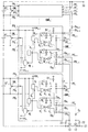
図1は、第1実施形態に係るバッテリ装置の回路構成図である。図1に示すように、第1実施形態に係るバッテリ装置は、直列接続されたn個のバッテリBT1〜BTn、各バッテリBT1〜BTn毎に並列接続されたn個のスイッチ(セルバランス用スイッチ回路)SW1〜SWn、各バッテリBT1〜BTnに対応して個別に設けられたn個のバッテリ状態監視回路BM1〜BMn、第1トランジスタ(充電用pチャネル型トランジスタ)10、第2トランジスタ(放電用pチャネル型トランジスタ)11、第1抵抗素子(第1バイアス用抵抗素子)20、第2抵抗素子(第2バイアス用抵抗素子)21、第1外部端子30及び第2外部端子31から構成されている。
Hereinafter, an embodiment of the present invention will be described with reference to the drawings.
[First Embodiment]
FIG. 1 is a circuit configuration diagram of the battery device according to the first embodiment. As shown in FIG. 1, the battery device according to the first embodiment includes n batteries BT 1 to BT n connected in series and n switches (cells) connected in parallel for each of the batteries BT 1 to BT n. balancing switch circuit) SW 1 to SW n, the battery BT 1 to BT n n number of battery state monitoring circuit BM 1 to Bm n provided individually corresponding to the first transistor (p-channel type transistor for charging ) 10, a second transistor (discharge p-channel transistor) 11, a first resistor element (first bias resistor element) 20, a second resistor element (second bias resistor element) 21, a first external terminal 30, and The second external terminal 31 is used.
バッテリ状態監視回路BM1は、過充電検出回路A1、第1NOR回路B1、第1出力トランジスタC1、ダイオードDo1、第1インバータD1、第2インバータE1、第1電流源F1、過放電検出回路G1、第2NOR回路H1、第2出力トランジスタI1、第3インバータJ1、第4インバータK1、第2電流源L1、セルバランス回路M1、第1電圧監視端子PA1、第2電圧監視端子PB1、第1送信端子PC1、第2送信端子PD1、第1受信端子PE1、第2受信端子PF1及び制御端子PG1を備えている。また、このような構成要素を備えるバッテリ状態監視回路BM1は、1チップのIC(半導体装置)として構成されている。 The battery state monitoring circuit BM 1 includes an overcharge detection circuit A 1 , a first NOR circuit B 1 , a first output transistor C 1 , a diode Do 1 , a first inverter D 1 , a second inverter E 1 , and a first current source F 1. , Overdischarge detection circuit G 1 , second NOR circuit H 1 , second output transistor I 1 , third inverter J 1 , fourth inverter K 1 , second current source L 1 , cell balance circuit M 1 , first voltage monitor A terminal PA 1 , a second voltage monitoring terminal PB 1 , a first transmission terminal PC 1 , a second transmission terminal PD 1 , a first reception terminal PE 1 , a second reception terminal PF 1 and a control terminal PG 1 are provided. Further, the battery state monitoring circuit BM 1 including such components is configured as a one-chip IC (semiconductor device).
他のバッテリ状態監視回路BM2〜BMnは、バッテリ状態監視回路BM1と同一の構成要素を備えているので符号のみを変えて図示する。例えば、バッテリ状態監視回路BM2における過充電検出回路の符号はA2とし、バッテリ状態監視回路BMnにおける過充電検出回路の符号はAnとする。他の構成要素についても同様である。
このようにバッテリ状態監視回路BM1〜BMnは全て同一の回路構成となっているので、以下ではバッテリBT1に対応するバッテリ状態監視回路BM1を代表的に用いて説明する。
The other battery state monitoring circuits BM 2 to BM n are provided with the same components as the battery state monitoring circuit BM 1 , so that only the reference numerals are changed for illustration. For example, the sign of the overcharge detection circuit included in the battery state monitoring circuit BM 2 is a A 2, the sign of the overcharge detection circuit included in the battery state monitoring circuit BM n is set to A n. The same applies to other components.
Since the battery state monitoring circuit BM 1 to Bm n has become all the same circuit configuration, the following description will the battery state monitoring circuit BM 1 corresponding to the battery BT 1 is used typically.
バッテリ状態監視回路BM1において、第1電圧監視端子PA1は、バッテリBT1の正極端子、スイッチSW1の一方の端子と接続されている。また、この第1電圧監視端子PA1は、バッテリ状態監視回路BM1内の正極側共通電源線と接続されている。第2電圧監視端子PB1は、バッテリBT1の負極端子、スイッチSW1の他方の端子と接続されている。また、この第2電圧監視端子PB1は、バッテリ状態監視回路BM1内の負極側共通電源線と接続されている。以下では、バッテリ状態監視回路BM1内の正極側共通電源線をVDD1、負極側共通電源線をVSS1とし、バッテリ状態監視回路BM2内の正極側共通電源線をVDD2、負極側共通電源線をVSS2とし、以下同様に、バッテリ状態監視回路BMn内の正極側共通電源線をVDDn、負極側共通電源線をVSSnとする。 In the battery state monitoring circuit BM 1, the first voltage monitoring terminal PA 1 is the positive terminal of the battery BT 1, and is connected to one terminal of the switch SW 1. The first voltage monitoring terminal PA 1 is connected to the positive common power line in the battery state monitoring circuit BM 1 . The second voltage monitoring terminal PB 1 is connected to the negative terminal of the battery BT 1 and the other terminal of the switch SW 1 . The second voltage monitoring terminal PB 1 is connected to a negative common power line in the battery state monitoring circuit BM 1 . In the following description, the positive common power line in the battery state monitoring circuit BM 1 is VDD 1 , the negative common power line is VSS 1, and the positive common power line in the battery state monitoring circuit BM 2 is VDD 2 , common to the negative side. The power supply line is VSS 2, and similarly, the positive common power line in the battery state monitoring circuit BM n is VDD n and the negative common power supply line is VSS n .
過充電検出回路A1は、一端が第1電圧監視端子PA1と接続され、他端が第2電圧監視端子PB1と接続されており、第1電圧監視端子PA1と第2電圧監視端子PB1との間の電圧(つまりバッテリBT1の電圧)を検出し、バッテリBT1の電圧が過充電電圧以上となった場合に、ハイレベルの過充電検出信号を第1NOR回路B1の一方の入力端子に出力する。また、この過充電検出回路A1は、バッテリBT1の電圧が過充電電圧未満の場合に、ローレベルの過充電検出信号を第1NOR回路B1に出力する。ここで、過充電電圧とは、充電可能な上限電圧を指す。なお、過充電検出回路A1は、過放電検出回路G1からハイレベルの過放電検出信号が入力された場合に動作を停止する機能を有する。 The overcharge detection circuit A 1 has one end connected to the first voltage monitoring terminal PA 1 and the other end connected to the second voltage monitoring terminal PB 1. The first voltage monitoring terminal PA 1 and the second voltage monitoring terminal When a voltage between PB 1 (that is, the voltage of battery BT 1 ) is detected and the voltage of battery BT 1 becomes equal to or higher than the overcharge voltage, a high level overcharge detection signal is sent to one side of first NOR circuit B 1 . Output to the input terminal. Further, the overcharge detection circuit A 1 outputs a low level overcharge detection signal to the first NOR circuit B 1 when the voltage of the battery BT 1 is less than the overcharge voltage. Here, the overcharge voltage refers to an upper limit voltage that can be charged. The overcharge detection circuit A 1 has a function of stopping the operation when a high level overdischarge detection signal is input from the overdischarge detection circuit G 1 .
第1NOR回路B1は、上記過充電検出信号と第1インバータD1の出力信号とを入力とし、これら両信号の否定論理和信号を第1出力トランジスタC1のゲート端子に出力する。第1出力トランジスタC1は、nチャネル型MOS(Metal Oxide Semiconductor)トランジスタであり、ゲート端子は第1NOR回路B1の出力端子と接続され、ドレイン端子はダイオードDo1のカソード端子と接続され、ソース端子はVSS1と接続されている。ダイオードDo1は、放電漏れ電流防止用のダイオードであり、カソード端子は第1出力トランジスタC1のドレイン端子と接続され、アノード端子は第1送信端子PC1と接続されている。 The first NOR circuit B 1 receives the overcharge detection signal and the output signal of the first inverter D 1 as inputs, and outputs a negative OR signal of these two signals to the gate terminal of the first output transistor C 1 . The first output transistor C 1 is an n-channel MOS (Metal Oxide Semiconductor) transistor, the gate terminal is connected to the output terminal of the first NOR circuit B 1 , the drain terminal is connected to the cathode terminal of the diode Do 1 , and the source The terminal is connected to VSS 1 . The diode Do 1 is a diode for preventing discharge leakage current, the cathode terminal is connected to the drain terminal of the first output transistor C 1 , and the anode terminal is connected to the first transmission terminal PC 1 .
第1インバータD1は、第2インバータE1の出力信号の論理反転信号を第1NOR回路B1に出力する。第2インバータE1は、入力端が第1受信端子PE1及び第1電流源F1の出力端と接続されており、当該入力端への入力信号の論理反転信号を第1インバータD1に出力する。第1電流源F1は、入力端がVDD1と接続され、出力端が第2インバータE1の入力端及び第1受信端子PE1と接続された電流源である。 The first inverter D 1 outputs a logical inversion signal of the output signal of the second inverter E 1 to the first NOR circuit B 1 . The second inverter E 1 has an input terminal connected to the first receiving terminal PE 1 and the output terminal of the first current source F 1 , and outputs a logical inversion signal of the input signal to the input terminal to the first inverter D 1 . Output. The first current source F 1 is a current source whose input terminal is connected to VDD 1 and whose output terminal is connected to the input terminal of the second inverter E 1 and the first reception terminal PE 1 .
過放電検出回路G1は、一端が第1電圧監視端子PA1と接続され、他端が第2電圧監視端子PB1と接続されており、第1電圧監視端子PA1と第2電圧監視端子PB1との間の電圧(つまりバッテリBT1の電圧)を検出し、バッテリBT1の電圧が過放電電圧未満となった場合に、ハイレベルの過放電検出信号を第2NOR回路H1の一方の入力端子、過充電検出回路A1及びセルバランス回路M1に出力する。また、この過放電検出回路G1は、バッテリBT1の電圧が過放電電圧以上の場合に、ローレベルの過放電検出信号を出力する。ここで、過放電電圧とは、放電可能な下限電圧を指す。 The overdischarge detection circuit G 1 has one end connected to the first voltage monitoring terminal PA 1 and the other end connected to the second voltage monitoring terminal PB 1, and the first voltage monitoring terminal PA 1 and the second voltage monitoring terminal detecting a voltage (i.e. voltage of the battery BT 1) between the PB 1, when the voltage of the battery BT 1 is becomes lower than the overdischarge voltage, one of the high level overdischarge detection signal of the 2NOR circuits H 1 Output terminal, overcharge detection circuit A 1 and cell balance circuit M 1 . Further, the overdischarge detector circuit G 1 is the voltage of the battery BT 1 is the case of the above overdischarge voltage, and outputs a low level overdischarge detection signal. Here, the overdischarge voltage refers to a lower limit voltage that can be discharged.
第2NOR回路H1は、上記過放電検出信号と第3インバータJ1の出力信号とを入力とし、これら両信号の否定論理和信号を第2出力トランジスタI1のゲート端子に出力する。第2出力トランジスタI1は、nチャネル型MOSトランジスタであり、ゲート端子は第2NOR回路H1の出力端子と接続され、ドレイン端子は第2送信端子PD1と接続され、ソース端子はVSS1と接続されている。 The second NOR circuit H 1 receives the overdischarge detection signal and the output signal of the third inverter J 1 as inputs, and outputs a negative OR signal of these two signals to the gate terminal of the second output transistor I 1 . The second output transistor I 1 is an n-channel MOS transistor, the gate terminal is connected to the output terminal of the second NOR circuit H 1 , the drain terminal is connected to the second transmission terminal PD 1, and the source terminal is VSS 1 . It is connected.
第3インバータJ1は、第4インバータK1の出力信号の論理反転信号を第2NOR回路H1出力する。第4インバータK1は、入力端が第2受信端子PF1及び第2電流源L1の出力端と接続されており、当該入力端への入力信号の論理反転信号を第4インバータK1に出力する。第2電流源L1は、入力端がVDD1と接続され、出力端が第4インバータL1の入力端及び第2受信端子PF1と接続された電流源である。 The third inverter J 1 outputs a logic inverted signal of the output signal of the fourth inverter K 1 to the second NOR circuit H 1 . The input terminal of the fourth inverter K 1 is connected to the second receiving terminal PF 1 and the output terminal of the second current source L 1 , and the logical inversion signal of the input signal to the input terminal is supplied to the fourth inverter K 1 . Output. The second current source L 1 is a current source whose input terminal is connected to VDD 1 and whose output terminal is connected to the input terminal of the fourth inverter L 1 and the second reception terminal PF 1 .
セルバランス回路M1は、一端が第1電圧監視端子PA1と接続され、他端が第2電圧監視端子PB1と接続されており、第1電圧監視端子PA1と第2電圧監視端子PB1との間の電圧(つまりバッテリBT1の電圧)を検出し、バッテリBT1の電圧がセルバランス電圧以上となった場合に、セルバランス信号を制御端子PG1を介してスイッチSW1に出力する。また、このセルバランス回路M1は、バッテリBT1の電圧がセルバランス電圧未満の場合、ローレベルのセルバランス信号を制御端子PG1を介してスイッチSW1に出力する。ここで、セルバランス電圧とは、バッテリBT1が過充電状態に近い状態となる時の過充電電圧以下の電圧(バッテリBT1の電圧を他のバッテリの電圧に揃えてセルバランスをとり始める時の電圧)を指す。なお、このセルバランス回路M1は、過放電検出回路G1からハイレベルの過放電検出信号が入力された場合に動作を停止する機能を有する。 The cell balance circuit M 1 has one end connected to the first voltage monitoring terminal PA 1 and the other end connected to the second voltage monitoring terminal PB 1, and the first voltage monitoring terminal PA 1 and the second voltage monitoring terminal PB. 1 is detected (that is, the voltage of the battery BT 1 ), and when the voltage of the battery BT 1 becomes equal to or higher than the cell balance voltage, the cell balance signal is output to the switch SW 1 via the control terminal PG 1. To do. The cell balance circuit M 1 outputs a low level cell balance signal to the switch SW 1 via the control terminal PG 1 when the voltage of the battery BT 1 is less than the cell balance voltage. Here, the cell balance voltage, when start taking cell balance by aligning overcharge voltage following voltage (the voltage of the battery BT 1 to the voltage of the other battery when the battery BT 1 is a state close to the overcharged state Voltage). The cell balance circuit M 1 has a function of stopping the operation when a high level over discharge detection signal is input from the over discharge detection circuit G 1 .
第1送信端子PC1は、第1トランジスタ10のゲート端子及び第1抵抗素子20の一端と接続されている。第2送信端子PD1は、第2トランジスタ11のゲート端子及び第2抵抗素子21の一端と接続されている。第1受信端子PE1は、バッテリ状態監視回路BM2の第1送信端子PC2と接続されている。第2受信端子PF1は、バッテリ状態監視回路BM2の第2送信端子PD2と接続されている。 The first transmission terminal PC 1 is connected to the gate terminal of the first transistor 10 and one end of the first resistance element 20. The second transmission terminal PD 1 is connected to the gate terminal of the second transistor 11 and one end of the second resistance element 21. The first reception terminal PE 1 is connected to the first transmission terminal PC 2 of the battery state monitoring circuit BM 2 . The second reception terminal PF 1 is connected to the second transmission terminal PD 2 of the battery state monitoring circuit BM 2 .
また、バッテリ状態監視回路BM2の第1受信端子PE2は、バッテリ状態監視回路BM3の第1送信端子PC3と接続され、バッテリ状態監視回路BM2の第2受信端子PF2は、バッテリ状態監視回路BM3の第2送信端子PD3と接続されている。以下同様に、バッテリ状態監視回路BM3〜BMnにおいて、上段側(バッテリBT1側)のバッテリ状態監視回路の第1受信端子と下段側(バッテリBTn側)のバッテリ状態監視回路の第1送信端子とが接続され、上段側のバッテリ状態監視回路の第2受信端子と下段側のバッテリ状態監視回路の第2送信端子とが接続されている。なお、最下段であるバッテリ状態監視回路BMnの第1受信端子PEn及び第2受信端子PFnはバッテリBTnの負極端子と接続されている。 The first receiving terminal PE 2 of the battery state monitoring circuit BM 2 is connected to a first transmitting terminal PC 3 of the battery state monitoring circuit BM 3, the second receiving terminal PF 2 of the battery state monitoring circuit BM 2, the battery The state monitoring circuit BM 3 is connected to the second transmission terminal PD 3 . Similarly, in the battery state monitoring circuits BM 3 to BM n , the first receiving terminal of the battery state monitoring circuit on the upper stage side (battery BT 1 side) and the first of the battery state monitoring circuit on the lower stage side (battery BT n side). The transmission terminal is connected, and the second reception terminal of the upper battery state monitoring circuit is connected to the second transmission terminal of the lower battery state monitoring circuit. The first receiving terminal PE n and the second receiving terminal PF n of the battery state monitoring circuit BM n which is the lowest stage are connected to the negative terminal of the battery BT n .
スイッチSW1は、バッテリBT1と並列に接続されており、制御端子PG1を介して入力されるセルバランス信号に応じて、2端子間(つまりバッテリBT1の正極端子と負極端子との間)の接続/非接続を切り替えるものである。なお、このスイッチSW1は、セルバランス信号が入力された場合にオン、つまり2端子間を接続状態に切り替える。他のスイッチSW2〜SWnについても同様である。 The switch SW 1 is connected in parallel with the battery BT 1, and between two terminals (that is, between the positive terminal and the negative terminal of the battery BT 1) according to the cell balance signal input via the control terminal PG 1. ) To switch connection / disconnection. The switch SW 1 is turned on when a cell balance signal is input, that is, switches between two terminals to a connected state. The same applies to the other switches SW 2 to SW n .
第1トランジスタ10は、pチャネル型MOSトランジスタであり、ゲート端子はバッテリ状態監視回路BM1の第1送信端子PC1及び第1抵抗素子20の一端と接続され、ドレイン端子は第2トランジスタ11のドレイン端子と接続され、ソース端子は第1抵抗素子20の他端及び第1外部端子30と接続されている。第2トランジスタ11は、pチャネル型MOSトランジスタであり、ゲート端子はバッテリ状態監視回路BM1の第2送信端子PD1及び第2抵抗素子21の一端と接続され、ドレイン端子は第1トランジスタ10のドレイン端子と接続され、ソース端子は第2抵抗素子21の他端及びバッテリBT1の正極端子と接続されている。一方、第2外部端子31は、最下段のバッテリBTnの負極端子と接続されている。 The first transistor 10 is a p-channel MOS transistor, the gate terminal is connected to the first transmission terminal PC 1 and one end of the first resistance element 20 of the battery state monitoring circuit BM 1 , and the drain terminal is the second transistor 11. The source terminal is connected to the other end of the first resistance element 20 and the first external terminal 30. The second transistor 11 is a p-channel type MOS transistor, a gate terminal connected to one end of the second transmission terminal PD 1 and the second resistor element 21 of the battery state monitoring circuit BM 1, the drain terminal of the first transistor 10 The drain terminal is connected, and the source terminal is connected to the other end of the second resistance element 21 and the positive terminal of the battery BT 1 . On the other hand, the second external terminal 31 is connected to the negative terminal of the lowermost battery BT n.
このように構成された本バッテリ装置は、第1外部端子30と第2外部端子31との間に負荷または充電器を接続することにより、放電または充電を行うものである。 The present battery device configured as described above discharges or charges by connecting a load or a charger between the first external terminal 30 and the second external terminal 31.
次に、上記のように構成された第1実施形態に係るバッテリ装置の動作について説明する。
(通常状態時)
まず、通常状態時、つまりバッテリBT1〜BTnの全ての電圧が、過充電電圧未満且つ過放電電圧以上の範囲に含まれている場合について説明する。このような通常状態時において、バッテリ状態監視回路BM1の過充電検出回路A1は、ローレベルの過充電検出信号を第1NOR回路B1に出力する。
Next, the operation of the battery device according to the first embodiment configured as described above will be described.
(Normal state)
First, a description will be given of a normal state, that is, a case where all the voltages of the batteries BT 1 to BT n are included in a range less than the overcharge voltage and more than the overdischarge voltage. In such a normal state, the overcharge detection circuit A 1 of the battery state monitoring circuit BM 1 outputs a low level overcharge detection signal to the first NOR circuit B 1 .
この時、バッテリ状態監視回路BM2の第1出力トランジスタC2はオンとなっているため(この理由については後述する)、バッテリ状態監視回路BM1の第2インバータE1の入力端子はローレベルとなり、第1インバータD1からローレベルの出力信号が第1NOR回路B1に出力される。第1NOR回路B1は、ローレベルの過充電検出信号とローレベルの第1インバータD1の出力信号が入力されるため、ハイレベルの否定論理和信号を第1出力トランジスタC1のゲート端子に出力する。これにより、第1出力トランジスタC1はオンとなるため、第1送信端子PC1はローレベルとなり、第1トランジスタ10はオンとなる。 At this time, since the first output transistor C 2 of the battery state monitoring circuit BM 2 is turned on (The reason for this will be described later), the input terminal of the second inverter E 1 of the battery state monitoring circuit BM 1 is low level Thus, a low level output signal is output from the first inverter D 1 to the first NOR circuit B 1 . Since the first NOR circuit B 1 receives the low level overcharge detection signal and the low level output signal of the first inverter D 1 , a high level negative OR signal is applied to the gate terminal of the first output transistor C 1. Output. As a result, the first output transistor C 1 is turned on, so that the first transmission terminal PC 1 is at a low level and the first transistor 10 is turned on.
ここで、バッテリ状態監視回路BM2の第1出力トランジスタC2がオンとなっている理由について説明する。最下段のバッテリ状態監視回路BMnの第1受信端子PEnはバッテリBTnの負極端子と接続されているため、第2インバータEnの入力端子は常にローレベルとなっている。従って、第1インバータDnは、常にローレベルの出力信号を第1NOR回路Bnに出力し、過充電検出回路Anは、ローレベルの過充電検出信号を第1NOR回路Bnに出力する。これにより、第1NOR回路Bnは、ハイレベルの否定論理和信号を第1出力トランジスタCnのゲート端子に出力し、バッテリ状態監視回路BMnの第1出力トランジスタCnはオンとなる。 The following describes why the first output transistor C 2 of the battery state monitoring circuit BM 2 is on. First receiving terminal PE n of the lowermost battery state monitoring circuit BM n because it is connected to the negative terminal of the battery BT n, the input terminal of the second inverter E n is always a low level. Therefore, the first inverter D n, always outputs the output signal of the low level to the 1NOR circuit B n, the overcharge detection circuit A n outputs the overcharge detection signal of Low to the first 1NOR circuit B n. Thus, the 1NOR circuit B n outputs the high level of NOR signal to the gate terminal of the first output transistor C n, the first output transistor C n of the battery state monitoring circuit BM n is turned on.
これにより、バッテリ状態監視回路BMn-1の第2インバータEn-1の入力端子はローレベルとなり、第1インバータDn-1からローレベルの出力信号が第1NOR回路Bn-1に出力される。一方、過充電検出回路An-1は、ローレベルの過充電検出信号を第1NOR回路Bn-1に出力するので、第1NOR回路Bn-1は、ハイレベルの否定論理和信号を第1出力トランジスタCn-1のゲート端子に出力する。これにより、バッテリ状態監視回路BMn-1の第1出力トランジスタCn-1はオンとなる。 Thus, the input terminal of the second inverter E n-1 of the battery state monitoring circuit BM n-1 becomes low level, the output signal of low level from the first inverter D n-1 is output to the second 1NOR circuit B n-1 Is done. On the other hand, the overcharge detector circuit A n-1, since outputs the overcharge detection signal of Low to the first 1NOR circuit B n-1, the 1NOR circuit B n-1 is a high level NOR signal first 1 is output to the gate terminal of the output transistor C n−1 . Thus, the first output transistor C n-1 of the battery state monitoring circuit BM n-1 is turned on.
上記のような動作が上段側のバッテリ状態監視回路と下段側のバッテリ状態監視回路とで繰り返され、バッテリ状態監視回路BM2の第1出力トランジスタC2がオンとなるのである。 The above-described operation is repeated in the upper side of the battery state monitoring circuit and the lower side of the battery state monitoring circuit is the first output transistor C 2 of the battery state monitoring circuit BM 2 is turned on.
また、このような通常状態時において、バッテリ状態監視回路BM1の過放電検出回路G1は、ローレベルの過放電検出信号を第2NOR回路H1に出力する。この時、バッテリ状態監視回路BM2の第2出力トランジスタI2もオンとなっているため、バッテリ状態監視回路BM1の第4インバータK1の入力端子はローレベルとなり、第3インバータJ1からローレベルの出力信号が第2NOR回路H1に出力される。第2NOR回路H1は、ローレベルの過放電検出信号とローレベルの第3インバータJ1の出力信号が入力されるため、ハイレベルの否定論理和信号を第2出力トランジスタI1のゲート端子に出力する。これにより、第2出力トランジスタI1はオンとなるため、第2送信端子PD1はローレベルとなり、第2トランジスタ11はオンとなる。 Further, in such a normal state, the overdischarge detector circuit G 1 of the battery state monitoring circuit BM 1 outputs the low level overdischarge detection signal to the 2NOR circuit H 1. At this time, since the second output transistor I 2 of the battery state monitoring circuit BM 2 is also turned on, the input terminal of the fourth inverter K 1 of the battery state monitoring circuit BM 1 becomes low level, the third inverter J 1 A low level output signal is output to the second NOR circuit H 1 . Since the second NOR circuit H 1 receives a low level overdischarge detection signal and a low level third inverter J 1 output signal, a high level negative OR signal is applied to the gate terminal of the second output transistor I 1. Output. Accordingly, since the second output transistor I 1 is turned on, the second transmission terminal PD 1 becomes low level, and the second transistor 11 is turned on.
以上のように通常状態時においては、第1トランジスタ10及び第2トランジスタ11がオンとなるため、バッテリ装置は充電及び放電可能な状態となる。 As described above, in the normal state, the first transistor 10 and the second transistor 11 are turned on, so that the battery device can be charged and discharged.
(過充電状態時)
次に、過充電状態時、つまり、第1外部端子30と第2外部端子31との間に充電器が接続されてバッテリBT1〜BTnが充電され、これらバッテリBT1〜BTnの少なくとも1つの電圧が過充電電圧以上となった場合について説明する。なお、以下では、バッテリBT2の電圧が過充電電圧以上となった場合を想定して説明する。
(When overcharged)
Next, in an overcharge state, that is, a charger is connected between the first external terminal 30 and the second external terminal 31 to charge the batteries BT 1 to BT n , and at least the batteries BT 1 to BT n are charged. A case where one voltage is equal to or higher than the overcharge voltage will be described. In the following description, it is assumed that the voltage of the battery BT 2 is equal to or higher than the overcharge voltage.
この場合、バッテリ状態監視回路BM2の過充電検出回路A2は、ハイレベルの過充電検出信号を第1NOR回路B2に出力する。この時、第1インバータD2からはローレベルの出力信号が出力されているため、第1NOR回路B2はローレベルの否定論理和信号を第1出力トランジスタC2のゲート端子に出力する。これにより、第1出力トランジスタC2はオフとなる。 In this case, the overcharge detector circuit A 2 of the battery state monitoring circuit BM 2 outputs the high level overcharge detection signal to the 1NOR circuit B 2. At this time, since a low level output signal is output from the first inverter D 2 , the first NOR circuit B 2 outputs a low level negative OR signal to the gate terminal of the first output transistor C 2 . As a result, the first output transistor C 2 is turned off.
つまり、第1電流源F1によって第2インバータE1の入力端子はハイレベルにプルアップされ、第1インバータD1からハイレベルの出力信号が第1NOR回路B1に出力される。一方、過充電検出回路A1は、ローレベルの過充電検出信号を第1NOR回路B1に出力するため、第1NOR回路B1は、ローレベルの否定論理和信号を第1出力トランジスタC1のゲート端子に出力する。これにより、第1出力トランジスタC1はオフとなる。 That is, the input terminal of the second inverter E 1 is pulled up to a high level by the first current source F 1 , and a high level output signal is output from the first inverter D 1 to the first NOR circuit B 1 . On the other hand, the overcharge detector circuit A 1 is for outputting an overcharge detection signal of low level to the 1NOR circuit B 1, the 1NOR circuit B 1 represents a low level NOR signal of the first output transistor C 1 Output to the gate terminal. As a result, the first output transistor C 1 is turned off.
上記のように第1出力トランジスタC1がオフになると、第1トランジスタ10のゲートは第1抵抗素子20によってハイレベルとなり、第1トランジスタ10はオフとなるので、充電器からの充電が禁止されることになる。 When the first output transistor C 1 is turned off as described above, the gate of the first transistor 10 is set to the high level by the first resistance element 20 and the first transistor 10 is turned off, so that charging from the charger is prohibited. Will be.
なお、上記の説明は、バッテリBT2の電圧が過充電電圧以上となった場合を想定したものであるが、他のバッテリの電圧が過充電電圧以上となった場合も同様である。つまり、過充電状態となったバッテリに対応するバッテリ状態監視回路から過充電状態が生じたことを上段側のバッテリ状態監視回路に通信し、このような通信が最上段であるバッテリ状態監視回路BM1まで到達することにより、第1トランジスタ10はオフとなり、充電器からの充電が禁止される。 The above description assumes that the voltage of the battery BT 2 is equal to or higher than the overcharge voltage, but the same applies to the case where the voltage of the other battery is equal to or higher than the overcharge voltage. That is, the battery state monitoring circuit corresponding to the overcharged battery communicates that the overcharged state has occurred to the upper battery state monitoring circuit, and such communication is the uppermost battery state monitoring circuit BM. By reaching 1 , the first transistor 10 is turned off, and charging from the charger is prohibited.
(過放電状態時)
次に、過放電状態時、つまり、第1外部端子30と第2外部端子31との間に負荷が接続されてバッテリBT1〜BTnが放電し、これらバッテリBT1〜BTnの少なくとも1つの電圧が過放電電圧未満となった場合について説明する。なお、以下では、バッテリBT2の電圧が過放電電圧未満となった場合を想定して説明する。
(Over discharge state)
Then, when over-discharge state, i.e., a first external terminal 30 load is connected to discharge the battery BT 1 to BT n between the second external terminal 31, at least of the battery BT 1 to BT n 1 A case where one voltage becomes less than the overdischarge voltage will be described. In the following description, it is assumed that the voltage of the battery BT 2 is less than the overdischarge voltage.
この場合、バッテリ状態監視回路BM2の過放電検出回路G2は、ハイレベルの過放電検出信号を第2NOR回路H2に出力する。この時、第3インバータJ2からはローレベルの出力信号が出力されているため、第2NOR回路H2はローレベルの否定論理和信号を第2出力トランジスタI2のゲート端子に出力する。これにより、第2出力トランジスタI2はオフとなる。 In this case, the overdischarge detector circuit G 2 of the battery state monitoring circuit BM 2 outputs the high level overdischarge detection signal to the 2NOR circuit H 2. At this time, from the third inverter J 2 the output signal of low level is output, the 2NOR circuit H 2 outputs the NOR signal of low level to the gate terminal of the second output transistor I 2. As a result, the second output transistor I 2 is turned off.
つまり、第2電流源L1によって第4インバータK1の入力端子はハイレベルにプルアップされ、第3インバータJ1からハイレベルの出力信号が第2NOR回路H1に出力される。一方、過放電検出回路G1は、ローレベルの過放電検出信号を第2NOR回路H1に出力するため、第2NOR回路H1は、ローレベルの否定論理和信号を第2出力トランジスタI1のゲート端子に出力する。これにより、第2出力トランジスタI1はオフとなる。 That is, the input terminal of the fourth inverter K 1 is pulled up to a high level by the second current source L 1 , and a high-level output signal is output from the third inverter J 1 to the second NOR circuit H 1 . On the other hand, the overdischarge detector circuit G 1 is for outputting a low level of the over-discharge detection signal to the 2NOR circuits H 1, second 2NOR circuits H 1 is the low level NOR signal of the second output transistor I 1 Output to the gate terminal. As a result, the second output transistor I 1 is turned off.
上記のように第2出力トランジスタI1がオフになると、第2トランジスタ11のゲートは第2抵抗素子21によってハイレベルとなり、第2トランジスタ11はオフとなるので、負荷への放電が禁止されることになる。 As described above, when the second output transistor I 1 is turned off, the gate of the second transistor 11 is set to the high level by the second resistance element 21 and the second transistor 11 is turned off, so that discharge to the load is prohibited. It will be.
また、このような過放電状態時において、過放電状態を検出した過放電検出回路G2は、ハイレベルの過放電検出信号を過充電検出回路A2及びセルバランス回路M2に出力する。これにより、過充電検出回路A2及びセルバランス回路M2は動作を停止するため、消費電力の低減を図ることができる。また、第1電圧監視端子PA2はバッテリ状態監視回路BM2のVDD電源端子を兼ねており、バッテリ状態監視回路BM2はバッテリBT2から電源が供給されているので、放電しすぎているバッテリBT2の電圧が低くなり、その分、バッテリ状態監視回路BM2の消費電力も小さくなる。 In such an overdischarge state, the overdischarge detection circuit G 2 that has detected the overdischarge state outputs a high level overdischarge detection signal to the overcharge detection circuit A 2 and the cell balance circuit M 2 . As a result, the overcharge detection circuit A 2 and the cell balance circuit M 2 stop operating, so that power consumption can be reduced. The first voltage monitoring terminal PA 2 also serves as a VDD power source terminal of the battery state monitoring circuit BM 2, the battery state monitoring circuit BM 2 is the power supply from the battery BT 2 is supplied, too discharged battery The voltage of BT 2 is lowered, and accordingly, the power consumption of the battery state monitoring circuit BM 2 is also reduced.
ここで、各バッテリで特性バラツキが生じたことにより、放電中にバッテリBT2の電圧が他のバッテリの電圧よりも早く低くなっている場合、バッテリ状態監視回路BM2の過放電検出回路G2が他のバッテリ状態監視回路よりも早く過放電検出信号を出力することになる。すると、第2トランジスタ11がオフし、放電が禁止される。この時、バッテリ状態監視回路BM2は他のバッテリ状態監視回路よりも消費電力が小さくなる。消費電力が小さくなった分、バッテリBT2は他のバッテリよりも放電スピードが遅くなり、他のバッテリは今まで通りに放電する。よって、放電しすぎているバッテリBT2の放電スピードが遅くなるので、バッテリ装置は各バッテリの電圧を揃える(セルバランスをとる)ことができる。 Here, by characteristic variation in the battery has occurred, when the voltage of the battery BT 2 during discharge is lower faster than the voltage of the other battery, the over-discharge detection circuit of the battery state monitoring circuit BM 2 G 2 Outputs an overdischarge detection signal earlier than other battery state monitoring circuits. Then, the second transistor 11 is turned off and discharge is prohibited. At this time, the battery state monitoring circuit BM 2 is the power consumption is smaller than the other battery state monitoring circuits. As the power consumption is reduced, the battery BT 2 has a slower discharge speed than the other batteries, and the other batteries are discharged as before. Therefore, since the discharging speed of the battery BT 2 that is excessively discharged becomes slow, the battery device can make the voltage of each battery uniform (cell balance).
なお、上記の説明は、バッテリBT2の電圧が過放電電圧未満となった場合を想定したものであるが、他のバッテリの電圧が過放電電圧未満となった場合も同様である。つまり、過放電状態となったバッテリに対応するバッテリ状態監視回路から過放電状態が生じたことを上段側のバッテリ状態監視回路に通信し、このような通信が最上段であるバッテリ状態監視回路BM1まで到達することにより、第2トランジスタ11はオフとなり、負荷への放電が禁止される。 The above description assumes that the voltage of the battery BT 2 becomes less than the overdischarge voltage, but the same applies to the case where the voltage of the other battery becomes less than the overdischarge voltage. That is, the battery state monitoring circuit corresponding to the battery in the overdischarged state communicates that the overdischarged state has occurred to the upper battery state monitoring circuit, and such communication is the uppermost battery state monitoring circuit BM. By reaching 1 , the second transistor 11 is turned off and discharge to the load is prohibited.
(セルバランス状態時)
次に、セルバランス状態時、つまり、第1外部端子30と第2外部端子31との間に充電器が接続されてバッテリBT1〜BTnが充電され、これらバッテリBT1〜BTnの少なくとも1つの電圧がセルバランス電圧以上となった場合について説明する。なお、以下では、バッテリBT2の電圧がセルバランス電圧以上となった場合を想定して説明する。
(In cell balance state)
Next, in the cell balance state, that is, a charger is connected between the first external terminal 30 and the second external terminal 31 to charge the batteries BT 1 to BT n , and at least these batteries BT 1 to BT n are charged. A case where one voltage is equal to or higher than the cell balance voltage will be described. In the following description, it is assumed that the voltage of the battery BT 2 is equal to or higher than the cell balance voltage.
この場合、バッテリ状態監視回路BM2のセルバランス回路M2は、セルバランス信号を制御端子PG2を介してスイッチSW2に出力する。これにより、スイッチSW2はオンし、充電されているバッテリBT2はスイッチSW2を介して放電する。 In this case, the cell balance circuit M 2 of the battery state monitoring circuit BM 2 outputs a cell balance signal to the switch SW 2 via the control terminal PG 2 . As a result, the switch SW 2 is turned on, and the charged battery BT 2 is discharged via the switch SW 2 .
ここで、各バッテリで特性バラツキが生じたことにより、充電中にバッテリBT2の電圧が他のバッテリの電圧よりも早く高くなっている場合、バッテリ状態監視回路BM2が他のバッテリ状態監視回路よりも早くセルバランス信号を出力することになる。すると、スイッチSW2が他のスイッチよりも早くオンし、バッテリBT2は他のバッテリと充電量の変化が異なることになる。例えば、バッテリBT2は他のバッテリよりも充電スピードが遅くなり、他のバッテリは今まで通りに充電される。または、バッテリBT2は放電し、他のバッテリは今まで通りに充電される。よって、充電されすぎているバッテリBT2の充電スピードが遅くなるので、または、充電されすぎているバッテリBT2が放電するので、バッテリ装置はセルバランスをとることができる。 Here, if the voltage of the battery BT 2 becomes higher than the voltage of the other battery during charging due to the characteristic variation in each battery, the battery state monitoring circuit BM 2 is switched to the other battery state monitoring circuit. The cell balance signal is output earlier than that. Then, the switch SW 2 is turned on earlier than the other switches, and the battery BT 2 is different in charge amount from other batteries. For example, the battery BT 2 has a slower charging speed than the other batteries, and the other batteries are charged as before. Alternatively, the battery BT 2 is discharged and the other batteries are charged as before. Therefore, since the charging speed of the battery BT 2 that is charged too much is slow, or the battery BT 2 that is charged too much is discharged, the battery device can achieve cell balance.
以下、上記のような動作を前提として、バッテリ状態監視回路BM1にダイオードDo1を設けることにより放電漏れ電流を防ぐことのできる理由について説明する。図2は、ダイオードDo1を設けなかった場合のバッテリ装置の回路構成を示している。例えば、図2において、負荷への放電中にバッテリBT1が過放電状態となり、第2トランジスタ11がオフとなった場合を想定する。この場合、最上段のバッテリ状態監視回路BM1の第1出力トランジスタC1はオフ状態となるが、第1出力トランジスタC1のドレイン・ゲート間にはカソード端子をドレイン側、アノード端子をソース側とする寄生ダイオードが存在するため、図2に示すような電流経路が形成される。これにより、バッテリBT2〜BTnの放電は停止せず、放電漏れ電流が生じてしまうことになる。一方、第1実施形態のバッテリ状態監視回路BM1によれば、第1出力トランジスタC1の寄生ダイオードに対して逆方向のダイオードDo1を設けているため、図2に示すような放電漏れ電流の発生を防止することができる。 Hereinafter, the reason why the discharge leakage current can be prevented by providing the diode Do 1 in the battery state monitoring circuit BM 1 on the assumption of the above operation will be described. FIG. 2 shows a circuit configuration of the battery device when the diode Do 1 is not provided. For example, in FIG. 2, the battery BT 1 during the discharge to the load is over-discharged, it is assumed that the second transistor 11 is turned off. In this case, the first output transistor C 1 of the uppermost battery state monitoring circuit BM 1 is turned off, but the cathode terminal is on the drain side and the anode terminal is on the source side between the drain and gate of the first output transistor C 1. Therefore, a current path as shown in FIG. 2 is formed. As a result, the discharge of the batteries BT 2 to BT n does not stop, and a discharge leakage current occurs. On the other hand, according to the battery state monitoring circuit BM 1 of the first embodiment, since the provided opposite direction of the diode Do 1 to the first output transistor C 1 of the parasitic diode, discharge leakage current as shown in FIG. 2 Can be prevented.
以上のように、第1実施形態に係るバッテリ装置では、放電漏れ電流の発生を防止することができ、従来のようにバッテリ同士の電圧バランスの崩れは発生しないため、バッテリ交換に費やすコストや手間などのユーザの負担を解消することが可能である。 As described above, in the battery device according to the first embodiment, the occurrence of discharge leakage current can be prevented, and the voltage balance between the batteries does not collapse unlike the conventional case. It is possible to eliminate the burden on the user.
〔第2実施形態〕
次に、第2実施形態に係るバッテリ装置について説明する。上記第1実施形態では、バッテリ状態監視回路における第1出力トランジスタ及び第2出力トランジスタとしてnチャネル型MOSトランジスタを使用した場合を想定して説明した。これに対し、第2実施形態では、第1出力トランジスタ及び第2出力トランジスタとしてpチャネル型MOSトランジスタを使用した場合のバッテリ装置について説明する。
[Second Embodiment]
Next, a battery device according to a second embodiment will be described. In the first embodiment, the case where n-channel MOS transistors are used as the first output transistor and the second output transistor in the battery state monitoring circuit has been described. In contrast, in the second embodiment, a battery device in the case where p-channel MOS transistors are used as the first output transistor and the second output transistor will be described.
図3は、第2実施形態に係るバッテリ装置の回路構成図である。この図3において、図1と同様の構成要素には同一符号を付し説明を省略する。なお、図1と区別するために、バッテリ状態監視回路の符号をBMA1〜BMAnとし、第1トランジスタの符号を12、第2トランジスタの符号を13、第1抵抗素子の符号を22、第2抵抗素子の符号を23とする。また、これらバッテリ状態監視回路BMA1〜BMAnの回路構成は同一であるので、最下段のバッテリ状態監視回路BMAnを代表的に用いて説明する。 FIG. 3 is a circuit configuration diagram of the battery device according to the second embodiment. In FIG. 3, the same components as those in FIG. In order to distinguish from FIG. 1, the battery state monitoring circuit is denoted by BMA 1 to BMA n , the first transistor is denoted by 12, the second transistor is denoted by 13, the first resistance element is denoted by 22, The reference numeral of the two-resistance element is 23. Since the circuit configurations of these battery state monitoring circuits BMA 1 to BMA n are the same, the description will be given by using the lowermost battery state monitoring circuit BMA n as a representative.
第2実施形態におけるバッテリ状態監視回路BMAnは、過充電検出回路An、第1NOR回路Bn、第1インバータQn、第1出力トランジスタRn、ダイオードDon、第2インバータSn、第1電流源Tn、過放電検出回路Gn、第2NOR回路Hn、第3インバータUn、第2出力トランジスタVn、第4インバータWn、第2電流源Xn、セルバランス回路Mn、第1電圧監視端子PAn、第2電圧監視端子PBn、第1送信端子PCn、第2送信端子PDn、第1受信端子PEn、第2受信端子PFn及び制御端子PGnを備えている。なお、このような構成要素を備えるバッテリ状態監視回路BMAnは、1チップのICとして構成されている。 The battery state monitoring circuit BMA n in the second embodiment, the overcharge detection circuit A n, the 1NOR circuit B n, the first inverter Q n, the first output transistor R n, diode Do n, second inverter S n, the first current source T n, overdischarge detector circuit G n, the 2NOR circuit H n, the third inverter U n, a second output transistor V n, the fourth inverter W n, the second current source X n, the cell balance circuit M n , First voltage monitoring terminal PA n , second voltage monitoring terminal PB n , first transmission terminal PC n , second transmission terminal PD n , first reception terminal PE n , second reception terminal PF n and control terminal PG n I have. Note that the battery state monitoring circuit BMA n including such components is configured as a one-chip IC.
第1NOR回路Bnは、過充電検出回路Anから出力される過充電検出信号と第2インバータSnの出力信号とを入力とし、これら両信号の否定論理和信号を第1インバータQnに出力する。第1インバータQnは、上記第1NOR回路Bnから入力される否定論理和信号の論理反転信号を第1出力トランジスタRnのゲート端子に出力する。第1出力トランジスタRnは、pチャネル型MOSトランジスタであり、ゲート端子は第1インバータQnの出力端子と接続され、ドレイン端子はダイオードDonのアノード端子と接続され、
ソース端子はVDDnと接続されている。ダイオードDonは、放電漏れ電流防止用のダイオードであり、アノード端子は第1出力トランジスタRnのドレイン端子と接続され、カソード端子は第1送信端子PCnと接続されている。
The first 1NOR circuit B n, the overcharge detection signal output from the overcharge detecting circuit A n and the output signal of the second inverter S n as input, a NOR signal of both signals to the first inverter Q n Output. The first inverter Q n, and outputs a logical inversion signal of the NOR signal that is input from the first 1NOR circuit B n to the gate terminal of the first output transistor R n. The first output transistor R n, a p-channel type MOS transistor, a gate terminal connected to the output terminal of the first inverter Q n, a drain terminal connected to the anode terminal of the diode Do n,
The source terminal is connected to VDD n . Diode Do n is a diode for discharging leakage current prevention, an anode terminal connected to the drain terminal of the first output transistor R n, a cathode terminal is connected to the first transmitting terminal PC n.
第2インバータSnは、入力端が第1受信端子PEn及び第1電流源Tnの入力端と接続されており、当該入力端への入力信号の論理反転信号を第1NOR回路Bnに出力する。第1電流源Tnは、入力端が第1受信端子PEn及び第2インバータSnの入力端と接続され、出力端がVSSnと接続された電流源である。 The second inverter S n has an input terminal connected to the first receiving terminal PE n and the input terminal of the first current source T n , and outputs a logically inverted signal of the input signal to the input terminal to the first NOR circuit B n . Output. The first current source T n, an input terminal connected to the input terminal of the first receiving terminal PE n and the second inverter S n, a current source having an output connected with the VSS n.
第2NOR回路Hnは、過放電検出回路Gnから出力される過放電検出信号と第4インバータWnの出力信号とを入力とし、これら両信号の否定論理和信号を第3インバータUnに出力する。第3インバータUnは、上記第2NOR回路Hnから入力される否定論理和信号の論理反転信号を第2出力トランジスタVnのゲート端子に出力する。第2出力トランジスタVnは、pチャネル型MOSトランジスタであり、ゲート端子は第3インバータUnの出力端子と接続され、ドレイン端子は第2送信端子PDnと接続され、ソース端子はVDDnと接続されている。 The first 2NOR circuit H n, and an output signal of the overdischarge detection signal and the fourth inverter W n output from the overdischarge detector circuit G n as input, a NOR signal of both signals to the third inverter U n Output. The third inverter U n, and outputs a logical inversion signal of the NOR signal that is input from the first 2NOR circuit H n to the gate terminal of the second output transistor V n. The second output transistor V n, a p-channel type MOS transistor, a gate terminal connected to the output terminal of the third inverter U n, a drain terminal connected to the second transmitting terminal PD n, a source terminal and VDD n It is connected.
第4インバータWnは、入力端が第2受信端子PFn及び第2電流源Xnの入力端と接続されており、当該入力端への入力信号の論理反転信号を第2NOR回路Hnに出力する。第2電流源Xnは、入力端が第2受信端子PFn及び第4インバータWnの入力端と接続され、出力端がVSSnと接続された電流源である。 The fourth inverter W n has an input terminal connected to the second receiving terminal PF n and the input terminal of the second current source X n , and outputs a logical inversion signal of the input signal to the input terminal to the second NOR circuit H n . Output. The second current source X n, an input terminal connected to the input end of the second receiving terminal PF n and the fourth inverter W n, a current source having an output connected with the VSS n.
第1送信端子PCnは、第1トランジスタ12のゲート端子及び第1抵抗素子22の一端と接続されている。第2送信端子PDnは、第2トランジスタ13のゲート端子及び第2抵抗素子23の一端と接続されている。第1受信端子PEnは、バッテリ状態監視回路BMAn-1の第1送信端子PCn-1と接続されている。第2受信端子PFnは、バッテリ状態監視回路BMAn-1の第2送信端子PDn-1と接続されている。 The first transmission terminal PC n is connected to the gate terminal of the first transistor 12 and one end of the first resistance element 22. The second transmission terminal PD n is connected to the gate terminal of the second transistor 13 and one end of the second resistance element 23. The first reception terminal PE n is connected to the first transmission terminal PC n−1 of the battery state monitoring circuit BMA n−1 . The second receiving terminal PF n, is connected to the second transmitting terminal PD n-1 of the battery state monitoring circuit BMA n-1.
同様に、他のバッテリ状態監視回路において、下段側(バッテリBTn側)のバッテリ状態監視回路の第1受信端子と上段側(バッテリBT1側)のバッテリ状態監視回路の第1送信端子とが接続され、下段側のバッテリ状態監視回路の第2受信端子と上段側のバッテリ状態監視回路の第2送信端子とが接続されている。なお、最上段であるバッテリ状態監視回路BMA1の第1受信端子PE1及び第2受信端子PF1はバッテリBT1の正極端子と接続されている。 Similarly, in another battery state monitoring circuit, the first receiving terminal of the battery state monitoring circuit on the lower stage side (battery BT n side) and the first transmission terminal of the battery state monitoring circuit on the upper stage side (battery BT 1 side) The second receiving terminal of the lower battery state monitoring circuit is connected to the second transmitting terminal of the upper battery state monitoring circuit. The first receiving terminal PE 1 and the second receiving terminal PF 1 of the battery state monitoring circuit BMA 1 which is the uppermost stage are connected to the positive terminal of the battery BT 1 .
第1トランジスタ12は、nチャネル型MOSトランジスタであり、ゲート端子はバッテリ状態監視回路BMAnの第1送信端子PCn及び第1抵抗素子22の一端と接続され、ドレイン端子は第2トランジスタ13のドレイン端子と接続され、ソース端子は第1抵抗素子22の他端及びバッテリBTnの負極端子と接続されている。第2トランジスタ13は、nチャネル型MOSトランジスタであり、ゲート端子はバッテリ状態監視回路BMAnの第2送信端子PDn及び第2抵抗素子23の一端と接続され、ドレイン端子は第2トランジスタ12のドレイン端子と接続され、ソース端子は第2抵抗素子23の他端及び第2外部端子31と接続されている。一方、第1外部端子30は、最上段のバッテリBT1の正極端子と接続されている。 The first transistor 12 is an n-channel type MOS transistor, a gate terminal connected to one end of the first transmission terminal PC n, and the first resistance element 22 of the battery state monitoring circuit BMA n, a drain terminal of the second transistor 13 is connected to the drain terminal, the source terminal is connected to the negative terminal of the other end and the battery BT n of the first resistive element 22. The second transistor 13 is an n-channel type MOS transistor, a gate terminal connected to one end of the second transmission terminal PD n and the second resistive element 23 of the battery state monitoring circuit BMA n, a drain terminal of the second transistor 12 The drain terminal is connected, and the source terminal is connected to the other end of the second resistance element 23 and the second external terminal 31. On the other hand, the first external terminal 30 is connected to the positive terminal of the uppermost battery BT 1 .
次に、上記のように構成された第2実施形態に係るバッテリ装置の動作について説明する。なお、セルバランス状態時の動作は第1実施形態と同様なので説明を省略する。 Next, the operation of the battery device according to the second embodiment configured as described above will be described. Since the operation in the cell balance state is the same as that of the first embodiment, the description is omitted.
(通常状態時)
まず、通常状態時、つまりバッテリBT1〜BTnの全ての電圧が、過充電電圧未満且つ過放電電圧以上の範囲に含まれている場合について説明する。このような通常状態時において、バッテリ状態監視回路BMAnの過充電検出回路Anは、ローレベルの過充電検出信号を第1NOR回路Bnに出力する。
(Normal state)
First, a description will be given of a normal state, that is, a case where all the voltages of the batteries BT 1 to BT n are included in a range less than the overcharge voltage and more than the overdischarge voltage. In such a normal state, the overcharge detection circuit A n of the battery state monitoring circuit BMA n outputs the overcharge detection signal of Low to the first 1NOR circuit B n.
この時、バッテリ状態監視回路BMAn-1の第1出力トランジスタRn-1はオンとなっているため(この理由については後述する)、バッテリ状態監視回路BMAnにおける第2インバータSnの入力端はハイレベルとなり、第2インバータSnからローレベルの出力信号が第1NOR回路Bnに出力される。第1NOR回路Bnは、ハイレベルの否定論理和信号を第1インバータQnに出力し、第1インバータQnはローレベルの論理反転信号を第1出力トランジスタRnのゲート端子に出力する。これにより、第1出力トランジスタRnはオンとなるため、第1送信端子PCnはハイレベルとなり、第1トランジスタ12はオンとなる。 At this time, since the first output transistor R n-1 of the battery state monitoring circuit BMA n-1 is turned on (The reason for this will be described later), the input of the second inverter S n of the battery state monitoring circuit BMA n end becomes high level, the output signal of low level from the second inverter S n is output to the 1NOR circuit B n. The first 1NOR circuit B n, and outputs a high level NOR signal to the first inverter Q n, the first inverter Q n outputs a logical inversion signal of the low level to the gate terminal of the first output transistor R n. As a result, the first output transistor R n is turned on, so that the first transmission terminal PC n is at a high level, and the first transistor 12 is turned on.
ここで、バッテリ状態監視回路BMAn-1の第1出力トランジスタRn-1がオンとなっている理由について説明する。最上段のバッテリ状態監視回路BMA1の第1受信端子PE1はバッテリBT1の正極端子と接続されているため、第2インバータS1の入力端は常にハイレベルとなっている。従って、第2インバータS1は、常にローレベルの出力信号を第1NOR回路B1に出力し、過充電検出回路A1は、ローレベルの過充電検出信号を第1NOR回路B1に出力する。これにより、第1NOR回路B1は、ハイレベルの否定論理和信号を第1インバータQ1に出力し、第1インバータQ1はローレベルの論理反転信号を第1出力トランジスタR1のゲート端子に出力する。これにより、バッテリ状態監視回路BMA1の第1出力トランジスタR1はオンとなる。 The following describes why the first output transistor R n-1 of the battery state monitoring circuit BMA n-1 is turned on. First receiving terminal PE 1 of the uppermost battery state monitoring circuit BMA 1 because it is connected to the positive terminal of the battery BT 1, a second input terminal of the inverter S 1 is always at the high level. Accordingly, the second inverter S 1 always outputs a low level output signal to the first NOR circuit B 1 , and the overcharge detection circuit A 1 outputs a low level overcharge detection signal to the first NOR circuit B 1 . Thus, the 1NOR circuit B 1 represents, outputs a high-level NOR signal to the first inverter Q 1, a first inverter Q 1 is logically inverted signal of the low level to the gate terminal of the first output transistor R 1 Output. Thus, the first output transistor R 1 of the battery state monitoring circuit BMA 1 is turned on.
この時、バッテリ状態監視回路BMA1の下段側であるバッテリ状態監視回路BMA2における第2インバータS2の入力端はハイレベルとなり、第2インバータS2からローレベルの出力信号が第1NOR回路B2に出力される。過充電検出回路A2は、ローレベルの過充電検出信号を出力するので、第1NOR回路B2は、ハイレベルの否定論理和信号を第1インバータQ2に出力し、第1インバータQ2はローレベルの論理反転信号を第1出力トランジスタR2のゲート端子に出力する。これにより、第1出力トランジスタR2はオンとなる。 At this time, the input terminal of the second inverter S 2 in the battery state monitoring circuit BMA 2 on the lower side of the battery state monitoring circuit BMA 1 is at the high level, and the low level output signal from the second inverter S 2 is the first NOR circuit B. Output to 2 . Since the overcharge detection circuit A 2 outputs a low level overcharge detection signal, the first NOR circuit B 2 outputs a high level negative logical sum signal to the first inverter Q 2 , and the first inverter Q 2 It outputs a logical inversion signal of low level to the gate terminal of the first output transistor R 2. As a result, the first output transistor R 2 is turned on.
上記のような動作が上段側のバッテリ状態監視回路と下段側のバッテリ状態監視回路とで繰り返され、バッテリ状態監視回路BMAn-1の第1出力トランジスタRn-1がオンとなるのである。 The above-described operation is repeated in the upper side of the battery state monitoring circuit and the lower side of the battery state monitoring circuit, the first output transistor R n-1 of the battery state monitoring circuit BMA n-1 is becoming the on state.
また、このような通常状態時において、バッテリ状態監視回路BMAnの過放電検出回路Gnは、ローレベルの過放電検出信号を第2NOR回路Hnに出力する。この時、バッテリ状態監視回路BMAn-1の第2出力トランジスタVn-1もオンとなっているため、バッテリ状態監視回路BMAnにおける第4インバータWnの入力端はハイレベルとなり、第4インバータWnからローレベルの出力信号が第2NOR回路Hnに出力される。第2NOR回路Hnは、ハイレベルの否定論理和信号を第3インバータUnに出力し、第3インバータUnはローレベルの論理反転信号を第2出力トランジスタVnのゲート端子に出力する。これにより、第2出力トランジスタVnはオンとなるため、第2送信端子PDnはハイレベルとなり、第2トランジスタ13はオンとなる。 Further, in such a normal state, the overdischarge detector circuit G n of the battery state monitoring circuit BMA n outputs a low level overdischarge detection signal to the 2NOR circuit H n. At this time, since the second output transistor V n−1 of the battery state monitoring circuit BMA n−1 is also on, the input terminal of the fourth inverter W n in the battery state monitoring circuit BMA n becomes high level, A low level output signal is output from the inverter W n to the second NOR circuit H n . The first 2NOR circuit H n, and outputs a high level NOR signal to the third inverter U n, and the third inverter U n outputs a logical inversion signal of the low level to the gate terminal of the second output transistor V n. As a result, the second output transistor V n is turned on, so that the second transmission terminal PD n is at a high level, and the second transistor 13 is turned on.
以上のように通常状態時においては、第1トランジスタ12及び第2トランジスタ13がオンとなるため、バッテリ装置は充電及び放電可能な状態となる。 As described above, in the normal state, the first transistor 12 and the second transistor 13 are turned on, so that the battery device can be charged and discharged.
(過充電状態時)
次に、過充電状態時、つまり、第1外部端子30と第2外部端子31との間に充電器が接続されてバッテリBT1〜BTnが充電され、これらバッテリBT1〜BTnの少なくとも1つの電圧が過充電電圧以上となった場合について説明する。なお、以下では、バッテリBTn-1の電圧が過充電電圧以上となった場合を想定して説明する。
(When overcharged)
Next, in an overcharge state, that is, a charger is connected between the first external terminal 30 and the second external terminal 31 to charge the batteries BT 1 to BT n , and at least the batteries BT 1 to BT n are charged. A case where one voltage is equal to or higher than the overcharge voltage will be described. In the following description, it is assumed that the voltage of the battery BT n-1 is equal to or higher than the overcharge voltage.
この場合、バッテリ状態監視回路BMAn-1の過充電検出回路An-1は、ハイレベルの過充電検出信号を第1NOR回路Bn-1に出力する。この時、第2インバータSn-1からはローレベルの出力信号が出力されているため、第1NOR回路Bn-1はローレベルの否定論理和信号を第1インバータQn-1に出力し、第1インバータQn-1はハイレベルの論理反転信号を第1出力トランジスタRn-1のゲート端子に出力する。これにより、第1出力トランジスタRn-1はオフとなる。 In this case, the overcharge detector circuit A n-1 of the battery state monitoring circuit BMA n-1 outputs the high level overcharge detection signal to the 1NOR circuit B n-1. At this time, since the low level output signal is output from the second inverter S n−1 , the first NOR circuit B n−1 outputs a low level negative logical sum signal to the first inverter Q n−1. The first inverter Q n−1 outputs a high level logic inversion signal to the gate terminal of the first output transistor R n−1 . As a result, the first output transistor R n-1 is turned off.
つまり、第1電流源Tnによって第2インバータSnの入力端子はローレベルにプルダウンされ、第2インバータSnからハイレベルの出力信号が第1NOR回路Bnに出力される。一方、過充電検出回路Anは、ローレベルの過充電検出信号を第1NOR回路Bnに出力するため、第1NOR回路Bnは、ローレベルの否定論理和信号を第1インバータQnに出力し、第1インバータQnはハイレベルの論理反転信号を第1出力トランジスタRnのゲート端子に出力する。これにより、第1出力トランジスタRnはオフとなる。 That is, the input terminal of the second inverter S n by the first current source T n is pulled down to a low level, the output signal of high level from the second inverter S n is output to the 1NOR circuit B n. On the other hand, the overcharge detector circuit A n is for outputting an overcharge detection signal of low level to the 1NOR circuit B n, the 1NOR circuit B n are output to the low level NOR signal to the first inverter Q n and, the first inverter Q n outputs a logical inversion signal of the high level to the gate terminal of the first output transistor R n. As a result, the first output transistor R n is turned off.
上記のように第1出力トランジスタRnがオフとなると、第1トランジスタ12のゲートは第1抵抗素子22によりローレベルとなり、第1トランジスタ12はオフとなるので、充電器からの充電が禁止されることになる。 When the first output transistor R n is turned off as described above, the gate of the first transistor 12 is set to a low level by the first resistance element 22 and the first transistor 12 is turned off, so that charging from the charger is prohibited. Will be.
なお、上記の説明は、バッテリBTn-1の電圧が過充電電圧以上となった場合を想定したものであるが、他のバッテリの電圧が過充電電圧以上となった場合も同様である。つまり、過充電状態となったバッテリに対応するバッテリ状態監視回路から過充電状態が生じたことを下段側のバッテリ状態監視回路に通信し、このような通信が最下段であるバッテリ状態監視回路BMAnまで到達することにより、第1トランジスタ12はオフとなり、充電器からの充電が禁止される。 The above description assumes that the voltage of the battery BT n-1 is equal to or higher than the overcharge voltage, but the same applies to the case where the voltage of the other battery is equal to or higher than the overcharge voltage. In other words, the battery state monitoring circuit corresponding to the battery that has become overcharged communicates that an overcharged state has occurred to the lower battery state monitoring circuit, and such communication is the lowest battery state monitoring circuit BMA. By reaching n , the first transistor 12 is turned off and charging from the charger is prohibited.
(過放電状態時)
次に、過放電状態時、つまり、第1外部端子30と第2外部端子31との間に負荷が接続されてバッテリBT1〜BTnが放電し、これらバッテリBT1〜BTnの少なくとも1つの電圧が過放電電圧未満となった場合について説明する。なお、以下では、バッテリBTn-1の電圧が過放電電圧未満となった場合を想定して説明する。
(Over discharge state)
Then, when over-discharge state, i.e., a first external terminal 30 load is connected to discharge the battery BT 1 to BT n between the second external terminal 31, at least of the battery BT 1 to BT n 1 A case where one voltage becomes less than the overdischarge voltage will be described. In the following description, it is assumed that the voltage of the battery BT n-1 is less than the overdischarge voltage.
この場合、バッテリ状態監視回路BMAn-1の過放電検出回路Gn-1は、ハイレベルの過放電検出信号を第2NOR回路Hn-1に出力する。この時、第4インバータWn-1からはローレベルの出力信号が出力されているため、第2NOR回路Hn-1はローレベルの否定論理和信号を第3インバータUn-1に出力し、第3インバータUn-1はハイレベルの論理反転信号を第2出力トランジスタVn-1のゲート端子に出力する。これにより、第2出力トランジスタVn-1はオフとなる。 In this case, the overdischarge detector circuit G n-1 of the battery state monitoring circuit BMA n-1 outputs the high level overdischarge detection signal to the 2NOR circuit H n-1. At this time, since the low-level output signal is output from the fourth inverter W n−1 , the second NOR circuit H n−1 outputs a low-level negative OR signal to the third inverter Un−1. The third inverter Un-1 outputs a high level logic inversion signal to the gate terminal of the second output transistor Vn -1 . As a result, the second output transistor V n-1 is turned off.
つまり、第2電流源Xnによって第4インバータWnの入力端子はローレベルにプルダウンされ、第4インバータWnからハイレベルの出力信号が第2NOR回路Hnに出力される。一方、過放電検出回路Gnは、ローレベルの過放電検出信号を第2NOR回路Hnに出力するため、第2NOR回路Hnは、ローレベルの否定論理和信号を第3インバータUnに出力し、第3インバータUnはハイレベルの論理反転信号を第2出力トランジスタVnのゲート端子に出力する。これにより、第2出力トランジスタVnはオフとなる。 That is, the input terminal of the fourth inverter W n by the second current source X n is pulled down to a low level, the output signal of high level from the fourth inverter W n is output to the second 2NOR circuit H n. On the other hand, the overdischarge detector circuit G n, in order to output the overdischarge detection signal of low level to the 2NOR circuit H n, the first 2NOR circuit H n, outputs a low-level NOR signal to the third inverter U n and, the third inverter U n outputs a logical inversion signal of the high level to the gate terminal of the second output transistor V n. As a result, the second output transistor V n is turned off.
上記のように第2出力トランジスタVnがオフとなると、第2トランジスタ13のゲートは第2抵抗素子23によりローベルとなり、第2トランジスタ13はオフとなるので、負荷への放電が禁止されることになる。 As described above, when the second output transistor V n is turned off, the gate of the second transistor 13 becomes low level by the second resistance element 23 and the second transistor 13 is turned off, so that discharge to the load is prohibited. become.
なお、上記の説明は、バッテリBTn-1の電圧が過放電電圧未満となった場合を想定したものであるが、他のバッテリの電圧が過放電電圧未満となった場合も同様である。つまり、過放電状態となったバッテリに対応するバッテリ状態監視回路から過放電状態が生じたことを下段側のバッテリ状態監視回路に通信し、このような通信が最下段であるバッテリ状態監視回路BMAnまで到達することにより、第2トランジスタ13はオフとなり、負荷への放電が禁止される。 The above description assumes that the voltage of the battery BT n-1 is less than the overdischarge voltage, but the same applies to the case where the voltage of the other battery is less than the overdischarge voltage. In other words, the battery state monitoring circuit corresponding to the battery that has become overdischarged communicates that the overdischarge state has occurred to the lower battery state monitoring circuit, and such communication is the lowest battery state monitoring circuit BMA. By reaching n , the second transistor 13 is turned off and discharge to the load is prohibited.
以下、上記のような動作を前提として、バッテリ状態監視回路BMAnにダイオードDonを設けることにより放電漏れ電流を防ぐことのできる理由について説明する。図4は、ダイオードDonを設けなかった場合のバッテリ装置の回路構成を示している。例えば、図4において、負荷への放電中にバッテリBTnが過放電状態となり、第2トランジスタ13がオフとなった場合を想定する。この場合、バッテリ状態監視回路BMAnの第1出力トランジスタRnはオフ状態となるが、第1出力トランジスタRnのドレイン・ゲート間にはカソード端子をソース側、アノード端子をドレイン側とする寄生ダイオードが存在するため、図4に示すような電流経路が形成される。これにより、バッテリBT1〜BTnー1の放電は停止せず、放電漏れ電流が生じてしまうことになる。一方、第2実施形態にのバッテリ状態監視回路BMAnによれば、第1出力トランジスタRnの寄生ダイオードに対して逆方向のダイオードDonを設けているため、図4に示すような放電漏れ電流の発生を防止することができる。 Hereinafter, assuming operation as described above will be described the reason why that can prevent discharge leakage current by providing a diode Do n in the battery state monitoring circuit BMA n. Figure 4 shows a circuit configuration of a battery device when not provided a diode Do n. For example, in FIG. 4, it is assumed that the battery BT n is in an overdischarged state during discharging to the load, and the second transistor 13 is turned off. In this case, the parasitic first output transistor R n of the battery state monitoring circuit BMA n is turned off, between the drain and gate of the first output transistor R n to the source side of the cathode terminal, an anode terminal and a drain-side Since the diode exists, a current path as shown in FIG. 4 is formed. As a result, the discharge of the batteries BT 1 to BT n −1 is not stopped, and a discharge leakage current is generated. On the other hand, according to the battery state monitoring circuit BMA n of the second embodiment, since the provided opposite direction of the diode Do n the parasitic diodes of the first output transistor R n, discharge leakage as shown in FIG. 4 Generation of current can be prevented.
以上のように、第2実施形態に係るバッテリ装置では、第1実施形態と同様に、放電漏れ電流の発生を防止することができ、従来のようにバッテリ同士の電圧バランスの崩れは発生しないため、バッテリ交換に費やすコストや手間などのユーザの負担を解消することが可能である。 As described above, in the battery device according to the second embodiment, as in the first embodiment, the occurrence of discharge leakage current can be prevented, and the voltage balance between the batteries does not collapse unlike the conventional case. In addition, it is possible to eliminate the burden on the user such as the cost and labor required for battery replacement.
〔第3実施形態〕
次に、第3実施形態に係るバッテリ装置について説明する。図5は、第3実施形態に係るバッテリ装置の回路構成図である。この図に示すように、第3実施形態では、第1実施形態のバッテリ状態監視回路に、2つのダイオードを設けた構成となっている。すなわち、バッテリ状態監視回路の符号をBMB1〜BMBnとすると、バッテリ状態監視回路BMB1は、第1実施形態の構成要素に加えて、第1ダイオード(第1クランプ用ダイオード)Da1、第2ダイオード(第2クランプ用ダイオード)Db1、第3ダイオード(第3クランプ用ダイオード)Dc1及び第4ダイオード(第4クランプ用ダイオード)Dd1を新たに備えている。他のバッテリ状態監視回路も同様である。以下では、バッテリ状態監視回路BMB1を代表的に用いて説明する。
[Third Embodiment]
Next, a battery device according to a third embodiment will be described. FIG. 5 is a circuit configuration diagram of the battery device according to the third embodiment. As shown in this figure, in the third embodiment, the battery state monitoring circuit of the first embodiment is provided with two diodes. That is, if the symbols of the battery state monitoring circuits are BMB 1 to BMB n , the battery state monitoring circuit BMB 1 includes the first diode (first clamping diode) Da 1 , the first diode in addition to the components of the first embodiment. A second diode (second clamp diode) Db 1 , a third diode (third clamp diode) Dc 1, and a fourth diode (fourth clamp diode) Dd 1 are newly provided. The same applies to other battery state monitoring circuits. Hereinafter, the battery state monitoring circuit BMB 1 will be described as a representative example.
第1ダイオードDa1は、アノード端子がVSS1と接続され、カソード端子が第1出力トランジスタC1のドレイン端子と接続されており、バッテリ状態監視回路の耐圧を越えるような電圧(例えば4.5V)に相当する逆方向電圧がアノード端子とカソード端子との間に印加された場合に逆方向電流を生じるような特性を有している。第2ダイオードDb1は、アノード端子がVSS1と接続され、カソード端子が第2インバータE1の入力端と接続されている。なお、第2ダイオードDb1の電圧降下分を0.7Vとする。 The first diode Da 1 has an anode terminal connected to VSS 1 and a cathode terminal connected to the drain terminal of the first output transistor C 1 , and a voltage (for example, 4.5 V) that exceeds the withstand voltage of the battery state monitoring circuit. ), A reverse current is generated when a reverse voltage is applied between the anode terminal and the cathode terminal. The second diode Db 1 has an anode terminal connected to VSS 1 and a cathode terminal connected to the input terminal of the second inverter E 1 . Note that the voltage drop of the second diode Db 1 is 0.7V.
第3ダイオードDc1は、アノード端子がVSS1と接続され、カソード端子が第2出力トランジスタI1のドレイン端子と接続されており、バッテリ状態監視回路の耐圧を越えるような電圧に相当する逆方向電圧がアノード端子とカソード端子との間に印加された場合に逆方向電流を生じるような特性を有している。第4ダイオードDd1は、アノード端子がVSS1と接続され、カソード端子が第4インバータK1の入力端と接続されている。なお、第4ダイオードDd1の電圧降下分を0.7Vとする。 The third diode Dc 1 has an anode terminal connected to VSS 1 and a cathode terminal connected to the drain terminal of the second output transistor I 1 , and has a reverse direction corresponding to a voltage exceeding the withstand voltage of the battery state monitoring circuit. When the voltage is applied between the anode terminal and the cathode terminal, the reverse current is generated. The fourth diode Dd 1 has an anode terminal connected to VSS 1 and a cathode terminal connected to the input terminal of the fourth inverter K 1 . Note that the voltage drop of the fourth diode Dd 1 is 0.7V.
また、下段側のバッテリ状態監視回路の第1送信端子と上段側のバッテリ状態監視回路の第1受信端子との間、さらに下段側のバッテリ状態監視回路の第2送信端子と上段側のバッテリ状態監視回路の第2受信端子との間に抵抗素子が接続されている。具体的には、バッテリ状態監視回路BMB2の第1送信端子PC2とバッテリ状態監視回路BMB1の第1受信端子PE1との間には抵抗素子Ra1が接続されており、バッテリ状態監視回路BMB2の第2送信端子PD2とバッテリ状態監視回路BMB1の第2受信端子PF1との間には抵抗素子Rb1が接続されている。 Further, between the first transmission terminal of the lower battery state monitoring circuit and the first reception terminal of the upper battery state monitoring circuit, the second transmission terminal of the lower battery state monitoring circuit and the upper battery state A resistance element is connected between the second receiving terminal of the monitoring circuit. Specifically, a resistive element Ra 1 is connected between the first receiving terminal PE 1 of the battery state monitoring circuit first transmitting terminal PC 2 and the battery state monitoring circuit BMB 1 of BMB 2, the battery state monitoring resistive element Rb 1 is connected between the second transmitting terminal PD 2 and the second receiving terminal PF 1 of the battery state monitoring circuit BMB 1 circuit BMB 2.
次に、このように構成された第3実施形態に係るバッテリ装置の動作について説明する。なお、セルバランス状態時の動作は第1実施形態と同様なので説明を省略する。 Next, the operation of the battery device according to the third embodiment configured as described above will be described. Since the operation in the cell balance state is the same as that of the first embodiment, the description is omitted.
(通常状態時)
まず、通常状態時、つまりバッテリBT1〜BTnの全ての電圧が、過充電電圧未満且つ過放電電圧以上の範囲に含まれている場合について説明する。このような通常状態時において、バッテリ状態監視回路BMB1の過充電検出回路A1は、ローレベルの過充電検出信号を第1NOR回路B1に出力する。
(Normal state)
First, a description will be given of a normal state, that is, a case where all the voltages of the batteries BT 1 to BT n are included in a range less than the overcharge voltage and more than the overdischarge voltage. In such a normal state, the overcharge detection circuit A 1 of the battery state monitoring circuit BMB 1 outputs a low-level overcharge detection signal to the first NOR circuit B 1 .
この時、バッテリ状態監視回路BMB2の第1出力トランジスタC2はオンとなっているため、バッテリ状態監視回路BMB1の第2インバータE1の入力端はローレベルとなり、第1インバータD1からローレベルの出力信号が第1NOR回路B1に出力される。第1NOR回路B1は、ハイレベルの否定論理和信号を第1出力トランジスタC1のゲート端子に出力する。これにより、第1出力トランジスタC1はオンとなるため、第1送信端子PC1はローレベルとなり、第1トランジスタ10はオンとなる。
ここで、バッテリ状態監視回路BMB2の第1出力トランジスタC2がオンになっていると、バッテリ状態監視回路BMB1の第1受信端子PE1は抵抗素子Ra1を介してVSS2に接続されることになる。しかしながら、第1受信端子PE1には第2ダイオードDb1を設けてあるので、その電圧はVSS1−0.7Vにクランプされ、それ以下に下がることはない。
At this time, since the first output transistor C 2 of the battery state monitoring circuit BMB 2 is turned on, a second input terminal of the inverter E 1 of the battery state monitoring circuit BMB 1 becomes low level, the first inverter D 1 A low level output signal is output to the first NOR circuit B 1 . The first NOR circuit B 1 outputs a high level negative OR signal to the gate terminal of the first output transistor C 1 . As a result, the first output transistor C 1 is turned on, so that the first transmission terminal PC 1 is at a low level and the first transistor 10 is turned on.
Here, when the first output transistor C 2 of the battery state monitoring circuit BMB 2 is turned on, the first receiving terminal PE 1 of the battery state monitoring circuit BMB 1 is connected to VSS 2 via the resistance element Ra 1. Will be. However, since the second diode Db 1 is provided at the first receiving terminal PE 1 , the voltage is clamped at VSS 1 −0.7 V and does not drop below that.
また、このような通常状態時において、バッテリ状態監視回路BMB1の過放電検出回路G1は、ローレベルの過放電検出信号を第2NOR回路H1に出力する。この時、バッテリ状態監視回路BMB2の第2出力トランジスタI2もオンとなっているため、バッテリ状態監視回路BMB1の第4インバータK1の入力端子はローレベルとなり、第3インバータJ1からローレベルの出力信号が第2NOR回路H1に出力される。第2NOR回路H1は、ハイレベルの否定論理和信号を第2出力トランジスタI1のゲート端子に出力する。これにより、第2出力トランジスタI1はオンとなるため、第2送信端子PD1はローレベルとなり、第2トランジスタ11はオンとなる。
バッテリ状態監視回路BMB1の第2受信端子PF1の電圧も同様に、VSS1−0.7Vにクランプされる。
Further, in such a normal state, the overdischarge detector circuit G 1 of the battery state monitoring circuit BMB 1 outputs the low level overdischarge detection signal to the 2NOR circuit H 1. At this time, since the second output transistor I 2 of the battery state monitoring circuit BMB 2 is also turned on, the input terminal of the fourth inverter K 1 of the battery state monitoring circuit BMB 1 becomes low level, the third inverter J 1 A low level output signal is output to the second NOR circuit H 1 . The second NOR circuit H 1 outputs a high level negative OR signal to the gate terminal of the second output transistor I 1 . Accordingly, since the second output transistor I 1 is turned on, the second transmission terminal PD 1 becomes low level, and the second transistor 11 is turned on.
Similarly, the voltage of the second receiving terminal PF 1 of the battery state monitoring circuit BMB 1 is clamped to VSS 1 −0.7V.
以上のように通常状態時においては、第1トランジスタ10及び第2トランジスタ11がオンとなるため、バッテリ装置は充電及び放電可能な状態となる。 As described above, in the normal state, the first transistor 10 and the second transistor 11 are turned on, so that the battery device can be charged and discharged.
(過充電状態時)
次に、過充電状態時、つまり、第1外部端子30と第2外部端子31との間に充電器が接続されてバッテリBT1〜BTnが充電され、これらバッテリBT1〜BTnの少なくとも1つの電圧が過充電電圧以上となった場合について説明する。なお、以下では、バッテリBT2の電圧が過充電電圧以上となった場合を想定して説明する。
(When overcharged)
Next, in an overcharge state, that is, a charger is connected between the first external terminal 30 and the second external terminal 31 to charge the batteries BT 1 to BT n , and at least the batteries BT 1 to BT n are charged. A case where one voltage is equal to or higher than the overcharge voltage will be described. In the following description, it is assumed that the voltage of the battery BT 2 is equal to or higher than the overcharge voltage.
この場合、バッテリ状態監視回路BMB2の過充電検出回路A2は、ハイレベルの過充電検出信号を第1NOR回路B2に出力する。この時、第1インバータD2からはローレベルの出力信号が出力されているため、第1NOR回路B2はローレベルの否定論理和信号を第1出力トランジスタC2のゲート端子に出力する。これにより、第1出力トランジスタC2はオフとなる。 In this case, the overcharge detector circuit A 2 of the battery state monitoring circuit BMB 2 outputs the high level overcharge detection signal to the 1NOR circuit B 2. At this time, since a low level output signal is output from the first inverter D 2 , the first NOR circuit B 2 outputs a low level negative OR signal to the gate terminal of the first output transistor C 2 . As a result, the first output transistor C 2 is turned off.
つまり、第1電流源F1によって第2インバータE1の入力端子はハイレベルにプルアップされる。これにより、第2インバータE1の入力端子にはハイレベルとして認識される電圧が印加され、第1インバータD1からハイレベルの出力信号が第1NOR回路B1に出力される。一方、過充電検出回路A1は、ローレベルの過充電検出信号を第1NOR回路B1に出力するため、第1NOR回路B1は、ローレベルの否定論理和信号を第1出力トランジスタC1のゲート端子に出力する。これにより、第1出力トランジスタC1はオフとなる。 That is, the input terminal of the second inverter E 1 is pulled up to a high level by the first current source F 1 . Thus, the second input terminal of the inverter E 1 a voltage is applied which is recognized as a high level, the output signal of high level from the first inverter D 1 are output to the 1NOR circuit B 1. On the other hand, the overcharge detector circuit A 1 is for outputting an overcharge detection signal of low level to the 1NOR circuit B 1, the 1NOR circuit B 1 represents a low level NOR signal of the first output transistor C 1 Output to the gate terminal. As a result, the first output transistor C 1 is turned off.
この時、バッテリ状態監視回路BMB2の第1送信端子PC2は抵抗素子Ra1を介してVDD1にプルアップされる。しかしながら、第1送信端子PC2には第1ダイオードDa2が設けられているので、端子電圧は第1ダイオードDa2の逆方向電流を生じるような電圧(4.5V)によってVSS2+4.5Vにクランプされる。また、抵抗素子Ra1の抵抗値を、第2インバータE1の入力端子の電圧が第1電流源F1によってハイレベルまでプルアップされるような値に設定する。 The first transmitting terminal PC 2 of the battery state monitoring circuit BMB 2 is pulled up to the VDD 1 through the resistive element Ra 1. However, since the first diode Da 2 is provided at the first transmission terminal PC 2 , the terminal voltage is VSS 2 +4.5 V due to a voltage (4.5 V) that generates a reverse current of the first diode Da 2. To be clamped. Further, the resistance value of the resistance element Ra 1 is set to such a value that the voltage at the input terminal of the second inverter E 1 is pulled up to a high level by the first current source F 1 .
上記のように第1出力トランジスタC1がオフとなると、第1トランジスタ10のゲートは第1抵抗素子20によりハイレベルとなり、第1トランジスタ10はオフとなるので、充電器からの充電が禁止されることになる。 When the first output transistor C 1 is turned off as described above, the gate of the first transistor 10 is set to the high level by the first resistance element 20 and the first transistor 10 is turned off, so that charging from the charger is prohibited. Will be.
(過放電状態時)
次に、過放電状態時、つまり、第1外部端子30と第2外部端子31との間に負荷が接続されてバッテリBT1〜BTnが放電し、これらバッテリBT1〜BTnの少なくとも1つの電圧が過放電電圧未満となった場合について説明する。なお、以下では、バッテリBT2の電圧が過放電電圧未満となった場合を想定して説明する。
(Over discharge state)
Then, when over-discharge state, i.e., a first external terminal 30 load is connected to discharge the battery BT 1 to BT n between the second external terminal 31, at least of the battery BT 1 to BT n 1 A case where one voltage becomes less than the overdischarge voltage will be described. In the following description, it is assumed that the voltage of the battery BT 2 is less than the overdischarge voltage.
この場合、バッテリ状態監視回路BMB2の過放電検出回路G2は、ハイレベルの過放電検出信号を第2NOR回路H2に出力する。この時、第3インバータJ2からはローレベルの出力信号が出力されているため、第2NOR回路H2はローレベルの否定論理和信号を第2出力トランジスタI2のゲート端子に出力する。これにより、第2出力トランジスタI2はオフとなる。 In this case, the overdischarge detector circuit G 2 of the battery state monitoring circuit BMB 2 outputs the high level overdischarge detection signal to the 2NOR circuit H 2. At this time, from the third inverter J 2 the output signal of low level is output, the 2NOR circuit H 2 outputs the NOR signal of low level to the gate terminal of the second output transistor I 2. As a result, the second output transistor I 2 is turned off.
つまり、第2電流源L1によって第4インバータK1の入力端子はハイレベルにプルアップされる。これにより、第4インバータK1の入力端子にはハイレベルとして認識される電圧が印加され、第3インバータJ1からハイレベルの出力信号が第2NOR回路H1に出力される。一方、過放電検出回路G1は、ローレベルの過放電検出信号を第2NOR回路H1に出力するため、第2NOR回路H1は、ローレベルの否定論理和信号を第2出力トランジスタI1のゲート端子に出力する。これにより、第2出力トランジスタI1はオフとなる。 That is, the input terminal of the fourth inverter K 1 is pulled up to a high level by the second current source L 1 . As a result, a voltage recognized as a high level is applied to the input terminal of the fourth inverter K 1 , and a high level output signal is output from the third inverter J 1 to the second NOR circuit H 1 . On the other hand, the overdischarge detector circuit G 1 is for outputting a low level of the over-discharge detection signal to the 2NOR circuits H 1, second 2NOR circuits H 1 is the low level NOR signal of the second output transistor I 1 Output to the gate terminal. As a result, the second output transistor I 1 is turned off.
この時、バッテリ状態監視回路BMB2の第2送信端子PD2は抵抗素子Rb1を介してVDD1にプルアップされる。しかしながら、第2送信端子PD2には第3ダイオードDc2が設けられているので、端子電圧は第3ダイオードDc2の逆方向電流が生じるような電圧(4.5V)によってVSS2+4.5Vにクランプされる。また、抵抗素子Rb1の抵抗値を、第4インバータK1の入力端子の電圧が第2電流源L1によってハイレベルまでプルアップされるような値に設定する。 In this case, the second transmitting terminal PD 2 of the battery state monitoring circuit BMB 2 is pulled up to the VDD 1 through the resistive element Rb 1. However, since the third diode Dc 2 is provided at the second transmission terminal PD 2 , the terminal voltage is VSS 2 +4.5 V due to a voltage (4.5 V) at which the reverse current of the third diode Dc 2 is generated. To be clamped. Further, the resistance value of the resistance element Rb 1 is set to such a value that the voltage at the input terminal of the fourth inverter K 1 is pulled up to a high level by the second current source L 1 .
上記のように第2出力トランジスタI1がオフとなると、第2トランジスタ11のゲートはハイレベルとなり、第2トランジスタ11はオフとなるので、負荷への放電が禁止されることになる。 When the second output transistor I 1 is turned off as described above, the gate of the second transistor 11 is at a high level and the second transistor 11 is turned off, so that discharging to the load is prohibited.
第1実施形態では、過充電状態または過放電状態を検出したバッテリ状態監視回路において、第1出力トランジスタまたは第2出力トランジスタはオフとなり、その上段側のバッテリ状態監視回路におけるプルアップ動作によって、オフとなった下段側の第1出力トランジスタまたは第2出力トランジスタには、2セル分(2つのバッテリ分)の電圧が印加されることになる。つまり、1つのバッテリ状態監視回路の耐圧は少なくとも2セル分の電圧以上あれば良いことになる。これに対し、第3実施形態では、過充電状態または過放電状態を検出したバッテリ状態監視回路において、第1出力トランジスタまたは第2出力トランジスタはオフとなり、その上段側のバッテリ状態監視回路におけるプルアップ動作によって、オフとなった下段側の第1出力トランジスタまたは第2出力トランジスタには、1セル分(1つのバッテリ分)の電圧が印加されることになる。つまり、1つのバッテリ状態監視回路の耐圧は少なくとも1セル分の電圧以上あれば良いことになる。従って、第3実施形態によれば、第1実施形態と比べてさらに低耐圧のバッテリ状態監視回路を作製することができ、使用できる製造プロセスの幅がさらに広がる。勿論、第1実施形態と同様に、放電漏れ電流の発生を防止することができ、従来のようにバッテリ同士の電圧バランスの崩れは発生しないため、バッテリ交換に費やすコストや手間などのユーザの負担を解消することが可能である。 In the first embodiment, in the battery state monitoring circuit that detects an overcharged state or an overdischarged state, the first output transistor or the second output transistor is turned off, and is turned off by the pull-up operation in the upper battery state monitoring circuit. A voltage corresponding to two cells (for two batteries) is applied to the lower-stage first output transistor or second output transistor. That is, it is sufficient that the withstand voltage of one battery state monitoring circuit is at least equal to the voltage for two cells. On the other hand, in the third embodiment, in the battery state monitoring circuit that detects the overcharge state or the overdischarge state, the first output transistor or the second output transistor is turned off, and the pull-up in the upper battery state monitoring circuit is performed. By the operation, a voltage corresponding to one cell (for one battery) is applied to the lower first output transistor or second output transistor that is turned off. That is, it is sufficient that the withstand voltage of one battery state monitoring circuit is at least a voltage for one cell. Therefore, according to the third embodiment, a battery state monitoring circuit having a lower withstand voltage than that of the first embodiment can be manufactured, and the range of usable manufacturing processes is further expanded. Of course, as in the first embodiment, the occurrence of a discharge leakage current can be prevented, and the voltage balance between the batteries does not collapse as in the prior art. Can be eliminated.
〔第4実施形態〕
次に、第4実施形態に係るバッテリ装置について説明する。図6は、第4実施形態に係るバッテリ装置の回路構成図である。この図に示すように、第4実施形態では、第2実施形態のバッテリ状態監視回路に、2つのダイオードを設けた構成となっている。すなわち、バッテリ状態監視回路の符号をBMC1〜BMCnとすると、バッテリ状態監視回路BMCnは、第2実施形態の構成要素に加えて、第1ダイオードDen、第2ダイオードDfn、第3ダイオードDgn及び第4ダイオードDhnを新たに備えている。他のバッテリ状態監視回路も同様である。以下では、バッテリ状態監視回路BMCnを代表的に用いて説明する。
[Fourth Embodiment]
Next, a battery device according to a fourth embodiment will be described. FIG. 6 is a circuit configuration diagram of the battery device according to the fourth embodiment. As shown in this figure, in the fourth embodiment, the battery state monitoring circuit of the second embodiment is provided with two diodes. That is, assuming that the symbols of the battery state monitoring circuits are BMC 1 to BMC n , the battery state monitoring circuit BMC n includes the first diode De n , the second diode Df n , the third diode in addition to the components of the second embodiment. the diode Dg n and the fourth diode Dh n has newly. The same applies to other battery state monitoring circuits. Hereinafter, the battery state monitoring circuit BMC n will be representatively described.
第1ダイオードDenは、アノード端子が第1出力トランジスタRnのドレイン端子と接続され、カソード端子がVDDnと接続されており、バッテリ状態監視回路の耐圧を越えるような電圧(例えば4.5V)に相当する逆方向電圧がアノード端子とカソード端子との間に印加された場合に逆方向電流を生じるような特性を有している。第2ダイオードDfnは、アノード端子が第2インバータSnの入力端子と接続され、カソード端子がVDDnと接続されている。なお、第2ダイオードDfnによる電圧降下分を0.7Vとする。 The first diode De n, the anode terminal is connected to the drain terminal of the first output transistor R n, a cathode terminal is connected to the VDD n, the voltage which exceeds the withstand voltage of the battery state monitoring circuit (e.g., 4.5V ), A reverse current is generated when a reverse voltage is applied between the anode terminal and the cathode terminal. The second diode Df n, the anode terminal connected to the input terminal of the second inverter S n, a cathode terminal connected to the VDD n. The voltage drop due to the second diode Df n is 0.7V.
第3ダイオードDgnは、アノード端子が第2出力トランジスタVnのドレイン端子と接続され、カソード端子がVDDnと接続されており、バッテリ状態監視回路の耐圧を越えるような電圧(例えば4.5V)に相当する逆方向電圧がアノード端子とカソード端子との間に印加された場合に逆方向電流を生じるような特性を有している。第4ダイオードDhnは、アノード端子が第4インバータWnの入力端子と接続され、カソード端子がVDDnと接続されている。なお、第4ダイオードDhnによる電圧降下分を0.7Vとする。 The third diode Dg n, the anode terminal is connected to the drain terminal of the second output transistor V n, a cathode terminal is connected to the VDD n, the voltage which exceeds the withstand voltage of the battery state monitoring circuit (e.g., 4.5V ), A reverse current is generated when a reverse voltage is applied between the anode terminal and the cathode terminal. The fourth diode Dh n has an anode terminal connected to the input terminal of the fourth inverter W n and a cathode terminal connected to VDD n . It is assumed that the voltage drop due to the fourth diode Dh n is 0.7V.
また、上段側のバッテリ状態監視回路の第1送信端子と下段側のバッテリ状態監視回路の第1受信端子との間、さらに上段側のバッテリ状態監視回路の第2送信端子と下段側のバッテリ状態監視回路の第2受信端子との間に抵抗素子が接続されている。具体的には、バッテリ状態監視回路BMCn-1の第1送信端子PCn-1とバッテリ状態監視回路BMCnの第1受信端子PEnとの間には抵抗素子Ran-1が接続されており、バッテリ状態監視回路BMCn-1の第2送信端子PDn-1とバッテリ状態監視回路BMCnの第2受信端子PFn-1との間には抵抗素子Rbn-1が接続されている。 Further, between the first transmission terminal of the upper battery state monitoring circuit and the first reception terminal of the lower battery state monitoring circuit, the second transmission terminal of the upper battery state monitoring circuit and the lower battery state A resistance element is connected between the second receiving terminal of the monitoring circuit. Specifically, the resistance element Ra n-1 is connected between the first receiving terminal PE n of the first transmission terminal PC n-1 and the battery state monitoring circuit BMC n of the battery state monitoring circuit BMC n-1 and which, is resistive element Rb n-1 is connected between the battery state monitoring circuit second receiving terminal PF n-1 of the BMC n-1 of the second transmitting terminal PD n-1 and the battery state monitoring circuit BMC n ing.
次に、このように構成された第4実施形態に係るバッテリ装置の動作について説明する。なお、セルバランス状態時の動作は第1実施形態と同様なので説明を省略する。 Next, the operation of the battery device according to the fourth embodiment configured as described above will be described. Since the operation in the cell balance state is the same as that of the first embodiment, the description is omitted.
(通常状態時)
まず、通常状態時、つまりバッテリBT1〜BTnの全ての電圧が、過充電電圧未満且つ過放電電圧以上の範囲に含まれている場合について説明する。このような通常状態時において、バッテリ状態監視回路BMCnの過充電検出回路Anは、ローレベルの過充電検出信号を第1NOR回路Bnに出力する。
(Normal state)
First, a description will be given of a normal state, that is, a case where all the voltages of the batteries BT 1 to BT n are included in a range less than the overcharge voltage and more than the overdischarge voltage. In such a normal state, the overcharge detection circuit A n of the battery state monitoring circuit BMC n outputs the overcharge detection signal of Low to the first 1NOR circuit B n.
この時、バッテリ状態監視回路BMCn-1の第1出力トランジスタRn-1はオンとなっているため、バッテリ状態監視回路BMCnにおける第2インバータSnの入力端はハイレベルとなり、第2インバータSnからローレベルの出力信号が第1NOR回路Bnに出力される。第1NOR回路Bnは、ハイレベルの否定論理和信号を第1インバータQnに出力し、第1インバータQnはローレベルの論理反転信号を第1出力トランジスタRnのゲート端子に出力する。これにより、第1出力トランジスタRnはオンとなるため、第1送信端子PCnはハイレベルとなり、第1トランジスタ12はオンとなる。 At this time, the first output transistor R n-1 of the battery state monitoring circuit BMC n-1 because it has turned on, the input terminal of the second inverter S n of the battery state monitoring circuit BMC n becomes high level, the second the output signal of low level is output to the second 1NOR circuit B n from the inverter S n. The first 1NOR circuit B n, and outputs a high level NOR signal to the first inverter Q n, the first inverter Q n outputs a logical inversion signal of the low level to the gate terminal of the first output transistor R n. As a result, the first output transistor R n is turned on, so that the first transmission terminal PC n is at a high level, and the first transistor 12 is turned on.
また、このような通常状態時において、バッテリ状態監視回路BMCnの過放電検出回路Gnは、ローレベルの過放電検出信号を第2NOR回路Hnに出力する。この時、バッテリ状態監視回路BMCn-1の第2出力トランジスタVn-1はオンとなっているため、バッテリ状態監視回路BMCnにおける第4インバータWnの入力端はハイレベルとなり、第4インバータWnからローレベルの出力信号が第2NOR回路Hnに出力される。第2NOR回路Hnは、ハイレベルの否定論理和信号を第3インバータUnに出力し、第3インバータUnはローレベルの論理反転信号を第2出力トランジスタVnのゲート端子に出力する。これにより、第2出力トランジスタVnはオンとなるため、第2送信端子PDnはハイレベルとなり、第2トランジスタ13はオンとなる。 Further, in such a normal state, the overdischarge detector circuit G n of the battery state monitoring circuit BMC n outputs a low level overdischarge detection signal to the 2NOR circuit H n. At this time, the second output transistor V n-1 of the battery state monitoring circuit BMC n-1 because it has turned on, the input terminal of the fourth inverter W n in the battery state monitoring circuit BMC n becomes high level, the fourth A low level output signal is output from the inverter W n to the second NOR circuit H n . The first 2NOR circuit H n, and outputs a high level NOR signal to the third inverter U n, and the third inverter U n outputs a logical inversion signal of the low level to the gate terminal of the second output transistor V n. As a result, the second output transistor V n is turned on, so that the second transmission terminal PD n is at a high level, and the second transistor 13 is turned on.
以上のように通常状態時においては、第1トランジスタ12及び第2トランジスタ13がオンとなるため、バッテリ装置は充電及び放電可能な状態となる。 As described above, in the normal state, the first transistor 12 and the second transistor 13 are turned on, so that the battery device can be charged and discharged.
(過充電状態時)
次に、過充電状態時、つまり、第1外部端子30と第2外部端子31との間に充電器が接続されてバッテリBT1〜BTnが充電され、これらバッテリBT1〜BTnの少なくとも1つの電圧が過充電電圧以上となった場合について説明する。なお、以下では、バッテリBTn-1の電圧が過充電電圧以上となった場合を想定して説明する。
(When overcharged)
Next, in an overcharge state, that is, a charger is connected between the first external terminal 30 and the second external terminal 31 to charge the batteries BT 1 to BT n , and at least the batteries BT 1 to BT n are charged. A case where one voltage is equal to or higher than the overcharge voltage will be described. In the following description, it is assumed that the voltage of the battery BT n-1 is equal to or higher than the overcharge voltage.
この場合、バッテリ状態監視回路BMCn-1の過充電検出回路An-1は、ハイレベルの過充電検出信号を第1NOR回路Bn-1に出力する。この時、第2インバータSn-1からはローレベルの出力信号が出力されているため、第1NOR回路Bn-1はローレベルの否定論理和信号を第1インバータQn-1に出力し、第1インバータQn-1はハイレベルの論理反転信号を第1出力トランジスタRn-1のゲート端子に出力する。これにより、第1出力トランジスタRn-1はオフとなる。 In this case, the overcharge detector circuit A n-1 of the battery state monitoring circuit BMC n-1 outputs the high level overcharge detection signal to the 1NOR circuit B n-1. At this time, since the low level output signal is output from the second inverter S n−1 , the first NOR circuit B n−1 outputs a low level negative logical sum signal to the first inverter Q n−1. The first inverter Q n−1 outputs a high level logic inversion signal to the gate terminal of the first output transistor R n−1 . As a result, the first output transistor R n-1 is turned off.
つまり、第1電流源Tnによって第2インバータSnの入力端子はローレベルにプルダウンされるが、そのプルダウン電圧がVDDn−4.5V以下となった場合に、バッテリ状態監視回路BMCn-1の第1ダイオードDen-1を介してVSSnに電流が流れることになる。つまり、第2インバータSnの入力端子はVDDn−4.5Vにクランプされることになるが、その状態では第2インバータSnの動作電圧(ローレベルとして認識する電圧)に満たないため、第2インバータSnの入力端子の電圧が動作電圧に到達するように抵抗素子Ran-1の抵抗値を設定する。 That is, when the first current source T n is the input terminal of the second inverter S n is pulled down to a low level, that the pull-down voltage becomes equal to or lower than VDD n -4.5 V, the battery state monitoring circuit BMC n- a current flows in the VSS n through a first diode De n-1 of 1. That is, since the input terminal of the second inverter S n is made to be clamped to VDD n -4.5 V, which in this state is less than the operating voltage of the second inverter S n (voltage recognized as low level), voltage at the input terminal of the second inverter S n to set the resistance value of the resistance element Ra n-1 to reach the operating voltage.
これにより、第2インバータSnの入力端子にはローレベルとして認識される電圧が印加され、第2インバータSnからハイレベルの出力信号が第1NOR回路Bnに出力される。一方、過充電検出回路Anは、ローレベルの過充電検出信号を第1NOR回路Bnに出力するため、第1NOR回路Bnは、ローレベルの否定論理和信号を第1インバータQnに出力し、第1インバータQnはハイレベルの論理反転信号を第1出力トランジスタRnのゲート端子に出力する。これにより、第1出力トランジスタRnはオフとなる。 Thus, the input terminal of the second inverter S n voltage recognized as low level is applied, the output signal of the high level from the second inverter S n is output to the 1NOR circuit B n. On the other hand, the overcharge detector circuit A n is for outputting an overcharge detection signal of low level to the 1NOR circuit B n, the 1NOR circuit B n are output to the low level NOR signal to the first inverter Q n and, the first inverter Q n outputs a logical inversion signal of the high level to the gate terminal of the first output transistor R n. As a result, the first output transistor R n is turned off.
上記のように第1出力トランジスタRnがオフとなると、第1トランジスタ12のゲートはローレベルとなり、第1トランジスタ12はオフとなるので、充電器からの充電が禁止されることになる。 When the first output transistor R n as described above is turned off, the gate of the first transistor 12 becomes low level, the first transistor 12 is therefore turned off, so that the charging from the charger is prohibited.
(過放電状態時)
次に、過放電状態時、つまり、第1外部端子30と第2外部端子31との間に負荷が接続されてバッテリBT1〜BTnが放電し、これらバッテリBT1〜BTnの少なくとも1つの電圧が過放電電圧未満となった場合について説明する。なお、以下では、バッテリBTn-1の電圧が過放電電圧未満となった場合を想定して説明する。
(Over discharge state)
Then, when over-discharge state, i.e., a first external terminal 30 load is connected to discharge the battery BT 1 to BT n between the second external terminal 31, at least of the battery BT 1 to BT n 1 A case where one voltage becomes less than the overdischarge voltage will be described. In the following description, it is assumed that the voltage of the battery BT n-1 is less than the overdischarge voltage.
この場合、バッテリ状態監視回路BMCn-1の過放電検出回路Gn-1は、ハイレベルの過放電検出信号を第2NOR回路Hn-1に出力する。この時、第4インバータWn-1からはローレベルの出力信号が出力されているため、第2NOR回路Hn-1はローレベルの否定論理和信号を第3インバータUn-1に出力し、第3インバータUn-1はハイレベルの論理反転信号を第2出力トランジスタVn-1のゲート端子に出力する。これにより、第2出力トランジスタVn-1はオフとなる。 In this case, the overdischarge detector circuit G n-1 of the battery state monitoring circuit BMC n-1 outputs the high level overdischarge detection signal to the 2NOR circuit H n-1. At this time, since the low-level output signal is output from the fourth inverter W n−1 , the second NOR circuit H n−1 outputs a low-level negative OR signal to the third inverter Un−1. The third inverter Un-1 outputs a high level logic inversion signal to the gate terminal of the second output transistor Vn -1 . As a result, the second output transistor V n-1 is turned off.
つまり、第2電流源Xnによって第4インバータWnの入力端子はローレベルにプルダウンされるが、そのプルダウン電圧がVDDn−4.5V以下となった場合に、バッテリ状態監視回路BMCn-1の第3ダイオードDgn-1を介してVSSnに電流が流れることになる。つまり、第4インバータWnの入力端子はVDDn−4.5Vにクランプされることになるが、その状態では第4インバータWnの動作電圧(ローレベルとして認識する電圧)に満たないため、第4インバータWnの入力端子の電圧が動作電圧に到達するように抵抗素子Rbn-1の抵抗値を設定する。 That is, the input terminal of the fourth inverter W n is pulled down to a low level by the second current source X n , but when the pull-down voltage becomes VDD n −4.5 V or less, the battery state monitoring circuit BMC n− A current flows to VSS n through one third diode Dgn −1 . That is, the input terminal of the fourth inverter W n is clamped to VDD n −4.5 V, but in this state, it is less than the operating voltage of the fourth inverter W n (voltage recognized as low level). The resistance value of the resistance element Rb n-1 is set so that the voltage at the input terminal of the fourth inverter W n reaches the operating voltage.
これにより、第4インバータWnの入力端子にはローレベルとして認識される電圧が印加され、第4インバータWnからハイレベルの出力信号が第2NOR回路Hnに出力される。一方、過放電検出回路Gnは、ローレベルの過放電検出信号を第2NOR回路Hnに出力するため、第2NOR回路Hnは、ローレベルの否定論理和信号を第3インバータUnに出力し、第3インバータUnはハイレベルの論理反転信号を第2出力トランジスタVnのゲート端子に出力する。これにより、第2出力トランジスタVnはオフとなる。 Thus, the input terminal of the fourth inverter W n a voltage is applied which is recognized as a low level, the output signal of high level from the fourth inverter W n is output to the second 2NOR circuit H n. On the other hand, the overdischarge detector circuit G n, in order to output the overdischarge detection signal of low level to the 2NOR circuit H n, the first 2NOR circuit H n, outputs a low-level NOR signal to the third inverter U n and, the third inverter U n outputs a logical inversion signal of the high level to the gate terminal of the second output transistor V n. As a result, the second output transistor V n is turned off.
上記のように第2出力トランジスタVnがオフとなると、第2トランジスタ13のゲートはローレベルとなり、第2トランジスタ13はオフとなるので、負荷への放電が禁止されることになる。 As described above, when the second output transistor V n is turned off, the gate of the second transistor 13 becomes low level, and the second transistor 13 is turned off, so that discharging to the load is prohibited.
以上のように、第4実施形態によれば、第3実施形態と同様に、1つのバッテリ状態監視回路の耐圧は少なくとも1セル分の電圧以上あれば良いことになる。従って、第4実施形態によれば、第2実施形態と比べてさらに低耐圧のバッテリ状態監視回路を作製することができ、使用できる製造プロセスの幅がさらに広がる。勿論、第2実施形態と同様に、放電漏れ電流の発生を防止することができ、従来のようにバッテリ同士の電圧バランスの崩れは発生しないため、バッテリ交換に費やすコストや手間などのユーザの負担を解消することが可能である。 As described above, according to the fourth embodiment, as with the third embodiment, it is sufficient that the withstand voltage of one battery state monitoring circuit is at least equal to the voltage for one cell. Therefore, according to the fourth embodiment, a battery state monitoring circuit having a lower breakdown voltage than that of the second embodiment can be manufactured, and the range of usable manufacturing processes is further expanded. Of course, as in the second embodiment, the occurrence of discharge leakage current can be prevented, and the voltage balance between the batteries does not collapse as in the conventional case. Can be eliminated.
〔第5実施形態〕
次に、第5実施形態に係るバッテリ装置について説明する。図7は、第5実施形態に係るバッテリ装置の回路構成図である。この図に示すように、第5実施形態では、第3実施形態においてバッテリ状態監視回路の外部に設けていた抵抗素子をバッテリ状態監視回路の内部に設けた構成となっている。
[Fifth Embodiment]
Next, a battery device according to a fifth embodiment will be described. FIG. 7 is a circuit configuration diagram of the battery device according to the fifth embodiment. As shown in this figure, the fifth embodiment has a configuration in which the resistance element provided outside the battery state monitoring circuit in the third embodiment is provided inside the battery state monitoring circuit.
バッテリ状態監視回路BMD1を代表的に用いて説明すると、バッテリ状態監視回路BMD1における第1受信端子PE1と第2ダイオードDb1のカソード端子との間に抵抗素子Ra1が接続されている。また、第2受信端子PF1と第4ダイオードDd1のカソード端子との間に抵抗素子Rb1が接続されている。
なお、動作については第3実施形態と同様なので説明を省略する。
The battery state monitoring circuit BMD 1 will be described as a representative example. The resistance element Ra 1 is connected between the first receiving terminal PE 1 and the cathode terminal of the second diode Db 1 in the battery state monitoring circuit BMD 1 . . Further, a resistance element Rb 1 is connected between the second reception terminal PF 1 and the cathode terminal of the fourth diode Dd 1 .
Since the operation is the same as that of the third embodiment, the description thereof is omitted.
このような構成とすることにより、バッテリ装置の製造者は、バッテリ状態監視回路BMD1をバッテリ数だけ用意し、抵抗素子を介さずに上段側と下段側のバッテリ状態監視回路を接続するだけで良く、製造工程の短縮に寄与することができる。なお、バッテリ状態監視回路の内部に抵抗素子を設けることは、バッテリ状態監視回路の大型化及びコスト増加を招く原因となるが、これを避けたい場合には第3実施形態を採用すれば良い。 With such a configuration, the manufacturer of the battery device only prepares the battery state monitoring circuit BMD 1 for the number of batteries, and only connects the upper and lower battery state monitoring circuits without a resistor element. It can contribute to shortening the manufacturing process. Note that providing a resistance element inside the battery state monitoring circuit causes an increase in size and cost of the battery state monitoring circuit, but the third embodiment may be adopted when it is desired to avoid this.
〔第6実施形態〕
次に、第6実施形態に係るバッテリ装置について説明する。図8は、第6実施形態に係るバッテリ装置の回路構成図である。この図に示すように、第6実施形態では、第4実施形態においてバッテリ状態監視回路の外部に設けていた抵抗素子をバッテリ状態監視回路の内部に設けた構成となっている。
[Sixth Embodiment]
Next, a battery device according to a sixth embodiment will be described. FIG. 8 is a circuit configuration diagram of the battery device according to the sixth embodiment. As shown in this figure, in the sixth embodiment, the resistance element provided outside the battery state monitoring circuit in the fourth embodiment is provided inside the battery state monitoring circuit.
バッテリ状態監視回路BMEnを代表的に用いて説明すると、バッテリ状態監視回路BMEnにおけるダイオードDonのアノード端子と第1ダイオードDenのアノード端子との間に抵抗素子Ranが接続されている。また、第3ダイオードDgnのアノード端子と第2送信端子PDnとの間に抵抗素子Rbnが接続されている。
なお、動作については第4実施形態と同様なので説明を省略する。
When the battery state monitoring circuit BME n will be described representatively with reference resistance element Ra n between the anode terminal of the anode terminal and the first diode De n diode Do n in the battery state monitoring circuit BME n are connected . The resistance element Rb n between the anode terminal and the second transmitting terminal PD n of the third diode Dg n are connected.
Since the operation is the same as that of the fourth embodiment, the description thereof is omitted.
このような構成とすることにより、バッテリ装置の製造者は、バッテリ状態監視回路BMEnをバッテリ数だけ用意し、抵抗素子を介さずに上段側と下段側のバッテリ状態監視回路を接続するだけで良く、製造工程の短縮に寄与することができる。なお、バッテリ状態監視回路の内部に抵抗素子を設けることは、バッテリ状態監視回路の大型化及びコスト増加を招く原因となるが、これを避けたい場合には第4実施形態を採用すれば良い。 With such a configuration, the manufacturer of the battery device only prepares the battery state monitoring circuit BME n by the number of batteries, and only connects the upper and lower battery state monitoring circuits without using a resistance element. It can contribute to shortening the manufacturing process. Note that providing a resistance element inside the battery state monitoring circuit causes an increase in the size and cost of the battery state monitoring circuit, but the fourth embodiment may be adopted to avoid this.
また、抵抗素子Ranを第2インバータSnの入力端子と第1受信端子PEnとの間に接続し、抵抗素子Rbnを第4インバータWnの入力端子と第2受信端子PFnとの間に接続するような構成としても良い。また、抵抗素子Ranを第2ダイオードDfnのアノード端子と第1受信端子PEnとの間に接続し、抵抗素子Rbnを第4ダイオードDhnのカソード端子と第2受信端子PFnとの間に接続するような構成としても良い。 Further, the resistive element Ra n connected between the input terminal and the first receiving terminal PE n of the second inverter S n, a resistor Rb n input terminal and the second receiving terminal PF n of the fourth inverter W n It is good also as a structure which connects between. Further, the resistive element Ra n connected between the anode terminal and the first receiving terminal PE n of the second diode Df n, a resistor Rb n and the cathode terminal and the second receiving terminal PF n of the fourth diode Dh n It is good also as a structure which connects between.
〔第7実施形態〕
次に、第7実施形態に係るバッテリ装置について説明する。図9は、第7実施形態に係るバッテリ装置の回路構成図である。この図に示すように、第7実施形態は、第1実施形態の各バッテリ状態監視回路BM1〜BMnに放電漏れ電流防止用のダイオードDo1〜Donを設けない場合のバッテリ装置である。なお、第1実施形態と区別するために、第7実施形態におけるバッテリ状態監視回路の符号をBM1’〜BMn’とする。第7実施形態では、放電漏れ電流防止用のダイオードDoを、バッテリ状態監視回路BM1’〜BMn’の外部に設ける。具体的には、ダイオードDoのアノード端子は第1トランジスタ10のゲート端子と接続され、カソード端子はバッテリ状態監視回路BM1の第1送信端子PC1と接続されている。
[Seventh Embodiment]
Next, a battery device according to a seventh embodiment will be described. FIG. 9 is a circuit configuration diagram of the battery device according to the seventh embodiment. As shown in this figure, the seventh embodiment is a battery device in the case without the diode Do 1 to DO n for discharging leakage current preventing the battery state monitoring circuit BM 1 to Bm n of the first embodiment . In order to distinguish the first embodiment, the sign of the battery state monitoring circuit in the seventh embodiment and BM 1 '~BM n'. In the seventh embodiment, a diode Do for preventing discharge leakage current is provided outside the battery state monitoring circuits BM 1 ′ to BM n ′. Specifically, the anode terminal of the diode Do are connected to the gate terminal of the first transistor 10, a cathode terminal connected to a first transmitting terminal PC 1 of the battery state monitoring circuit BM 1.
このような構成のバッテリ装置とすることにより、第1実施形態と同様に、放電漏れ電流の発生を防止することができ、従来のようにバッテリ同士の電圧バランスの崩れは発生しないため、バッテリ交換に費やすコストや手間などのユーザの負担を解消することが可能である。また、バッテリ状態監視回路内に放電漏れ電流防止用のダイオードを設ける必要がないため、コストの低減及び回路サイズの小型化を図ることができる。 By using the battery device having such a configuration, it is possible to prevent the occurrence of a discharge leakage current as in the first embodiment, and there is no disruption of the voltage balance between the batteries as in the prior art. It is possible to eliminate the burden on the user such as the cost and labor required for the operation. In addition, since it is not necessary to provide a diode for preventing discharge leakage current in the battery state monitoring circuit, the cost can be reduced and the circuit size can be reduced.
〔第8実施形態〕
次に、第8実施形態に係るバッテリ装置について説明する。図10は、第8実施形態に係るバッテリ装置の回路構成図である。この図に示すように、第8実施形態は、第2実施形態の各バッテリ状態監視回路BMA1〜BMAnに放電漏れ電流防止用のダイオードDo1〜Donを設けない場合のバッテリ装置である。なお、第2実施形態と区別するために、第8実施形態におけるバッテリ状態監視回路の符号をBMA1’〜BMAn’とする。第8実施形態では、放電漏れ電流防止用のダイオードDoを、バッテリ状態監視回路BMA1’〜BAMn’の外部に設ける。具体的には、ダイオードDoのカソード端子は第1トランジスタ12のゲート端子と接続され、アノード端子はバッテリ状態監視回路BMAnの第1送信端子PCnと接続されている。
[Eighth Embodiment]
Next, a battery device according to an eighth embodiment will be described. FIG. 10 is a circuit configuration diagram of the battery device according to the eighth embodiment. As shown in this figure, the eighth embodiment is a battery device in the case without the diode Do 1 to DO n for discharging leakage current preventing the battery state monitoring circuit BMA 1 ~BMA n of the second embodiment . In order to distinguish the second embodiment, the sign of the battery state monitoring circuit according to the eighth embodiment and BMA 1 '~BMA n'. In the eighth embodiment, a diode Do for preventing discharge leakage current is provided outside the battery state monitoring circuits BMA 1 ′ to BAM n ′. Specifically, the cathode terminal of the diode Do are connected to the gate terminal of the first transistor 12, the anode terminal is connected to the first transmitting terminal PC n of the battery state monitoring circuit BMA n.
このような構成のバッテリ装置とすることにより、第2実施形態と同様に、放電漏れ電流の発生を防止することができ、従来のようにバッテリ同士の電圧バランスの崩れは発生しないため、バッテリ交換に費やすコストや手間などのユーザの負担を解消することが可能である。また、バッテリ状態監視回路内に放電漏れ電流防止用のダイオードを設ける必要がないため、コストの低減及び回路サイズの小型化を図ることができる。 By using the battery device having such a configuration, it is possible to prevent the occurrence of a discharge leakage current as in the second embodiment, and the voltage balance between the batteries does not collapse unlike the conventional case. It is possible to eliminate the burden on the user such as the cost and labor required for the operation. In addition, since it is not necessary to provide a diode for preventing discharge leakage current in the battery state monitoring circuit, the cost can be reduced and the circuit size can be reduced.
〔第9実施形態〕
次に、第9実施形態に係るバッテリ装置について説明する。図11は、第9実施形態に係るバッテリ装置の回路構成図である。この図に示すように、第9実施形態は、第3実施形態の各バッテリ状態監視回路BMB1〜BMBnに放電漏れ電流防止用のダイオードDo1〜Donを設けない場合のバッテリ装置である。なお、第3実施形態と区別するために、第9実施形態におけるバッテリ状態監視回路の符号をBMB1’〜BMBn’とする。第9実施形態では、放電漏れ電流防止用のダイオードDoを、バッテリ状態監視回路BMB1’〜BMBn’の外部に設ける。具体的には、ダイオードDoのアノード端子は第1トランジスタ10のゲート端子と接続され、カソード端子はバッテリ状態監視回路BMB1の第1送信端子PC1と接続されている。
[Ninth Embodiment]
Next, a battery device according to a ninth embodiment will be described. FIG. 11 is a circuit configuration diagram of the battery device according to the ninth embodiment. As shown in this figure, the ninth embodiment is the battery device of the case without the diode Do 1 to DO n for discharging leakage current preventing the battery state monitoring circuit BMB 1 ~BMB n of the third embodiment . In order to distinguish the third embodiment, the sign of the battery state monitoring circuit according to the ninth embodiment and BMB 1 '~BMB n'. In the ninth embodiment, a diode Do for preventing discharge leakage current is provided outside the battery state monitoring circuits BMB 1 ′ to BMB n ′. Specifically, the anode terminal of the diode Do are connected to the gate terminal of the first transistor 10, a cathode terminal connected to a first transmitting terminal PC 1 of the battery state monitoring circuit BMB 1.
このような構成のバッテリ装置とすることにより、第3実施形態と同様に、放電漏れ電流の発生を防止することができ、従来のようにバッテリ同士の電圧バランスの崩れは発生しないため、バッテリ交換に費やすコストや手間などのユーザの負担を解消することが可能である。また、バッテリ状態監視回路内に放電漏れ電流防止用のダイオードを設ける必要がないため、コストの低減及び回路サイズの小型化を図ることができる。 By using the battery device having such a configuration, as in the third embodiment, the occurrence of discharge leakage current can be prevented, and the voltage balance between the batteries does not collapse unlike the conventional case. It is possible to eliminate the burden on the user such as the cost and labor required for the operation. In addition, since it is not necessary to provide a diode for preventing discharge leakage current in the battery state monitoring circuit, the cost can be reduced and the circuit size can be reduced.
〔第10実施形態〕
次に、第10実施形態に係るバッテリ装置について説明する。図12は、第10実施形態に係るバッテリ装置の回路構成図である。この図に示すように、第10実施形態は、第4実施形態の各バッテリ状態監視回路BMC1〜BMCnに放電漏れ電流防止用のダイオードDo1〜Donを設けない場合のバッテリ装置である。なお、第4実施形態と区別するために、第10実施形態におけるバッテリ状態監視回路の符号をBMC1’〜BMCn’とする。第10実施形態では、放電漏れ電流防止用のダイオードDoを、バッテリ状態監視回路BMC1’〜BACn’の外部に設ける。具体的には、ダイオードDoのカソード端子は第1トランジスタ12のゲート端子と接続され、アノード端子はバッテリ状態監視回路BMCnの第1送信端子PCnと接続されている。
[Tenth embodiment]
Next, a battery device according to a tenth embodiment will be described. FIG. 12 is a circuit configuration diagram of the battery device according to the tenth embodiment. As shown in this figure, the tenth embodiment is the battery device of the case without the diode Do 1 to DO n for discharging leakage current preventing the battery state monitoring circuit BMC 1 ~BMC n of the fourth embodiment . In order to distinguish the fourth embodiment, the sign of the battery state monitoring circuit in the tenth embodiment and the BMC 1 '~BMC n'. In the tenth embodiment, a diode Do for preventing discharge leakage current is provided outside the battery state monitoring circuits BMC 1 ′ to BAC n ′. Specifically, the cathode terminal of the diode Do are connected to the gate terminal of the first transistor 12, the anode terminal is connected to the first transmitting terminal PC n of the battery state monitoring circuit BMC n.
このような構成のバッテリ装置とすることにより、第4実施形態と同様に、放電漏れ電流の発生を防止することができ、従来のようにバッテリ同士の電圧バランスの崩れは発生しないため、バッテリ交換に費やすコストや手間などのユーザの負担を解消することが可能である。また、バッテリ状態監視回路内に放電漏れ電流防止用のダイオードを設ける必要がないため、コストの低減及び回路サイズの小型化を図ることができる。 By using the battery device having such a configuration, as in the fourth embodiment, it is possible to prevent the occurrence of a discharge leakage current, and the voltage balance between the batteries does not collapse as in the conventional case. It is possible to eliminate the burden on the user such as the cost and labor required for the operation. In addition, since it is not necessary to provide a diode for preventing discharge leakage current in the battery state monitoring circuit, the cost can be reduced and the circuit size can be reduced.
〔第11実施形態〕
次に、第11実施形態に係るバッテリ装置について説明する。図13は、第11実施形態に係るバッテリ装置の回路構成図である。この図に示すように、第11実施形態は、第5実施形態の各バッテリ状態監視回路BMD1〜BMDnに放電漏れ電流防止用のダイオードDo1〜Donを設けない場合のバッテリ装置である。なお、第5実施形態と区別するために、第11実施形態におけるバッテリ状態監視回路の符号をBMD1’〜BMDn’とする。第11実施形態では、放電漏れ電流防止用のダイオードDoを、バッテリ状態監視回路BMD1’〜BMDn’の外部に設ける。具体的には、ダイオードDoのアノード端子は第1トランジスタ10のゲート端子と接続され、カソード端子はバッテリ状態監視回路BMD1の第1送信端子PC1と接続されている。
[Eleventh embodiment]
Next, a battery device according to an eleventh embodiment will be described. FIG. 13 is a circuit configuration diagram of the battery device according to the eleventh embodiment. As shown in this figure, the eleventh embodiment is a battery device in the case without the diode Do 1 to DO n for discharging leakage current preventing the battery state monitoring circuit BMD 1 ~BMD n of the fifth embodiment . In order to distinguish the fifth embodiment, the sign of the battery state monitoring circuit in the eleventh embodiment and BMD 1 '~BMD n'. In the eleventh embodiment, a diode Do for preventing discharge leakage current is provided outside the battery state monitoring circuits BMD 1 ′ to BMD n ′. Specifically, the anode terminal of the diode Do are connected to the gate terminal of the first transistor 10, a cathode terminal connected to a first transmitting terminal PC 1 of the battery state monitoring circuit BMD 1.
このような構成のバッテリ装置とすることにより、第5実施形態と同様に、放電漏れ電流の発生を防止することができ、従来のようにバッテリ同士の電圧バランスの崩れは発生しないため、バッテリ交換に費やすコストや手間などのユーザの負担を解消することが可能である。また、バッテリ状態監視回路内に放電漏れ電流防止用のダイオードを設ける必要がないため、コストの低減及び回路サイズの小型化を図ることができる。 By using the battery device having such a configuration, as in the fifth embodiment, the occurrence of discharge leakage current can be prevented, and the voltage balance between the batteries does not collapse unlike the conventional case. It is possible to eliminate the burden on the user such as the cost and labor required for the operation. In addition, since it is not necessary to provide a diode for preventing discharge leakage current in the battery state monitoring circuit, the cost can be reduced and the circuit size can be reduced.
〔第12実施形態〕
次に、第12実施形態に係るバッテリ装置について説明する。図14は、第12実施形態に係るバッテリ装置の回路構成図である。この図に示すように、第12実施形態は、第6実施形態の各バッテリ状態監視回路BME1〜BMEnに放電漏れ電流防止用のダイオードDo1〜Donを設けない場合のバッテリ装置である。なお、第6実施形態と区別するために、第12実施形態におけるバッテリ状態監視回路の符号をBME1’〜BMEn’とする。第12実施形態では、放電漏れ電流防止用のダイオードDoを、バッテリ状態監視回路BME1’〜BAEn’の外部に設ける。具体的には、ダイオードDoのカソード端子は第1トランジスタ12のゲート端子と接続され、アノード端子はバッテリ状態監視回路BMEnの第1送信端子PCnと接続されている。
[Twelfth embodiment]
Next, a battery device according to a twelfth embodiment will be described. FIG. 14 is a circuit configuration diagram of the battery device according to the twelfth embodiment. As shown in this figure, the twelfth embodiment is a battery device in the case without the diode Do 1 to DO n for discharging leakage current preventing the battery state monitoring circuit BME 1 ~BME n of the sixth embodiment . Additionally, to distinguish from the sixth embodiment, the sign of the battery state monitoring circuit in the twelfth embodiment and BME 1 '~BME n'. In the twelfth embodiment, a diode Do for preventing discharge leakage current is provided outside the battery state monitoring circuits BME 1 ′ to BAE n ′. Specifically, the cathode terminal of the diode Do are connected to the gate terminal of the first transistor 12, the anode terminal is connected to the first transmitting terminal PC n of the battery state monitoring circuit BME n.
このような構成のバッテリ装置とすることにより、第6実施形態と同様に、放電漏れ電流の発生を防止することができ、従来のようにバッテリ同士の電圧バランスの崩れは発生しないため、バッテリ交換に費やすコストや手間などのユーザの負担を解消することが可能である。また、バッテリ状態監視回路内に放電漏れ電流防止用のダイオードを設ける必要がないため、コストの低減及び回路サイズの小型化を図ることができる。 By using the battery device having such a configuration, as in the sixth embodiment, it is possible to prevent the occurrence of a discharge leakage current, and there is no disruption of the voltage balance between the batteries as in the prior art. It is possible to eliminate the burden on the user such as the cost and labor required for the operation. In addition, since it is not necessary to provide a diode for preventing discharge leakage current in the battery state monitoring circuit, the cost can be reduced and the circuit size can be reduced.
BT1〜BTn…バッテリ、SW1〜SWn…スイッチ、BM1〜BMn…バッテリ状態監視回路、10…第1トランジスタ、11…第2トランジスタ、20…第1抵抗素子、21…第2抵抗素子、30…第1外部端子、31…第2外部端子、A1…過充電検出回路、B1…第1NOR回路、C1…第1出力トランジスタ、Do1、Do…ダイオード、D1…第1インバータ、E1…第2インバータ、F1…第1電流源、G1…過放電検出回路、H1…第2NOR回路、I1…第2出力トランジスタ、J1…第3インバータ、K1…第4インバータ、L1…第2電流源、M1…セルバランス回路、PA1…第1電圧監視端子、PB1…第2電圧監視端子、PC1…第1送信端子、PD1…第2送信端子、PE1…第1受信端子、PF1…第2受信端子、PG1…制御端子 BT 1 to BT n ... battery, SW 1 to SW n ... switch, BM 1 to BM n ... battery state monitoring circuit, 10 ... first transistor, 11 ... second transistor, 20 ... first resistance element, 21 ... second resistance element, 30 ... first external terminal, 31 ... second external terminal, A 1 ... overcharge detection circuit, B 1 ... first 1NOR circuit, C 1 ... first output transistor, Do 1, Do ... diodes, D 1 ... First inverter, E 1 ... second inverter, F 1 ... first current source, G 1 ... overdischarge detection circuit, H 1 ... second NOR circuit, I 1 ... second output transistor, J 1 ... third inverter, K 1 ... fourth inverter, L 1 ... second current source, M 1 ... cell balance circuit, PA 1 ... first voltage monitoring terminal, PB 1 ... second voltage monitoring terminal, PC 1 ... first transmission terminal, PD 1 ... second transmission terminal, PE 1 ... first receiving terminal, PF 1 ... second Shin terminal, PG 1 ... control terminal
Claims (17)
前記バッテリの負極端子との接続に用いられると共に内部の負極側共通電源線と接続された第2電圧監視端子と、
第1送信端子と、
第2送信端子と、
第1受信端子と、
第2受信端子と、
セルバランス制御端子と、
前記バッテリ状態検出回路として、前記第1電圧監視端子と前記第2電圧監視端子との間の電圧に基づいて、前記バッテリが過充電状態か否かを検出し、当該検出結果を示す過充電検出信号を出力する過充電検出回路と、
前記バッテリ状態検出回路として、前記第1電圧監視端子と前記第2電圧監視端子との間の電圧に基づいて、前記バッテリが過放電状態か否かを検出し、当該検出結果を示す過放電検出信号を出力する過放電検出回路と、
前記バッテリ状態検出回路として、前記第1電圧監視端子と前記第2電圧監視端子との間の電圧に基づいて、前記バッテリをセルバランス制御する必要があるか否かを検出し、当該検出結果を示すセルバランス信号を前記セルバランス制御端子に出力するセルバランス回路と、
第一の入力が前記第1受信端子と接続され、第二の入力が前記過充電検出回路の出力に接続される第一論理回路と、
入力端子が前記正極側共通電源線と接続され、出力端子が前記第1受信端子と接続された第1電流源と、
前記第一論理回路の出力信号をゲート端子の入力とし、ソース端子が前記負極側共通電源線と接続されたnチャネル型の第1トランジスタと、
第一の入力が前記第2受信端子と接続され、第二の入力が前記過放電検出回路の出力に接続される第二論理回路と、
入力端子が前記正極側共通電源線と接続され、出力端子が前記第2受信端子と接続された第2電流源と、
前記第二論理回路の出力信号をゲート端子の入力とし、ドレイン端子が前記第2送信端子と接続され、ソース端子が前記負極側共通電源線と接続されたnチャネル型の第2トランジスタと、を備え、
前記第一送信端子と前記第1トランジスタのドレイン端子との間に、前記第1トランジスタの2端子間における寄生ダイオードに対して逆向きに接続されたダイオードを備える、ことを特徴とするバッテリ状態監視回路。 A first voltage monitoring terminal used for connection to the positive terminal of one battery and connected to the internal positive power supply line;
A second voltage monitoring terminal connected to the negative side common power supply line of the internal together used for connection to the negative terminal of the battery,
A first transmission terminal;
A second transmission terminal;
A first receiving terminal;
A second receiving terminal;
A cell balance control terminal;
As the battery state detection circuit, based on the voltage between the first voltage monitoring terminal and the second voltage monitoring terminal, it is detected whether or not the battery is in an overcharged state, and an overcharge detection indicating the detection result An overcharge detection circuit that outputs a signal;
As the battery state detection circuit, based on the voltage between the first voltage monitoring terminal and the second voltage monitoring terminal, it is detected whether or not the battery is in an overdischarge state, and an overdischarge detection indicating the detection result An overdischarge detection circuit for outputting a signal;
Based on the voltage between the first voltage monitoring terminal and the second voltage monitoring terminal, the battery state detection circuit detects whether or not the battery needs to be subjected to cell balance control. A cell balance circuit for outputting a cell balance signal indicating to the cell balance control terminal;
A first logic circuit having a first input connected to the first receiving terminal and a second input connected to an output of the overcharge detection circuit;
A first current source having an input terminal connected to the positive common power line and an output terminal connected to the first receiving terminal;
An n-channel first transistor having an output signal of the first logic circuit as an input of a gate terminal and a source terminal connected to the negative-side common power line;
A second logic circuit having a first input connected to the second receiving terminal and a second input connected to an output of the overdischarge detection circuit;
A second current source having an input terminal connected to the positive common power line and an output terminal connected to the second receiving terminal;
An n-channel second transistor having an output signal of the second logic circuit as an input of a gate terminal, a drain terminal connected to the second transmission terminal, and a source terminal connected to the negative common power line; Prepared,
A battery state monitor comprising a diode connected in a reverse direction to a parasitic diode between two terminals of the first transistor between the first transmission terminal and the drain terminal of the first transistor. circuit.
前記バッテリの負極端子との接続に用いられると共に内部の負極側共通電源線と接続された第2電圧監視端子と、
第1送信端子と、
第2送信端子と、
第1受信端子と、
第2受信端子と、
セルバランス制御端子と、
前記バッテリ状態検出回路として、前記第1電圧監視端子と前記第2電圧監視端子との間の電圧に基づいて、前記バッテリが過充電状態か否かを検出し、当該検出結果を示す過充電検出信号を出力する過充電検出回路と、
前記バッテリ状態検出回路として、前記第1電圧監視端子と前記第2電圧監視端子との間の電圧に基づいて、前記バッテリが過放電状態か否かを検出し、当該検出結果を示す過放電検出信号を出力する過放電検出回路と、
前記バッテリ状態検出回路として、前記第1電圧監視端子と前記第2電圧監視端子との間の電圧に基づいて、前記バッテリをセルバランス制御する必要があるか否かを検出し、当該検出結果を示すセルバランス信号を前記セルバランス制御端子に出力するセルバランス回路と、
第一の入力が前記第1受信端子と接続され、第二の入力が前記過充電検出回路の出力に接続される第一論理回路と、
前記第一論理回路の出力信号をゲート端子の入力とし、ソース端子が前記正極側共通電源線と接続されたpチャネル型の第1トランジスタと、
入力端子が前記第1受信端子と接続され、出力端子が前記負極側共通電源線と接続された第1電流源と、
第一の入力が前記第2受信端子と接続され、第二の入力が前記過放電検出回路の出力に接続される第二論理回路と、
前記第二論理回路の出力信号をゲート端子の入力とし、ドレイン端子が前記第2送信端子と接続され、ソース端子が前記正極側共通電源線と接続されたpチャネル型の第2トランジスタと、
入力端子が前記第2受信端子と接続され、出力端子が前記負極側共通電源線と接続された第2電流源と、を備え、
前記第一送信端子と前記第1トランジスタのドレイン端子との間に、前記第1トランジスタの2端子間における寄生ダイオードに対して逆向きに接続されたダイオードを備える、ことを特徴とするバッテリ状態監視回路。 A first voltage monitoring terminal used for connection to the positive terminal of one battery and connected to the internal positive power supply line;
A second voltage monitoring terminal connected to the negative side common power supply line of the internal together used for connection to the negative terminal of the battery,
A first transmission terminal;
A second transmission terminal;
A first receiving terminal;
A second receiving terminal;
A cell balance control terminal;
As the battery state detection circuit, based on the voltage between the first voltage monitoring terminal and the second voltage monitoring terminal, it is detected whether or not the battery is in an overcharged state, and an overcharge detection indicating the detection result An overcharge detection circuit that outputs a signal;
As the battery state detection circuit, based on the voltage between the first voltage monitoring terminal and the second voltage monitoring terminal, it is detected whether or not the battery is in an overdischarge state, and an overdischarge detection indicating the detection result An overdischarge detection circuit for outputting a signal;
Based on the voltage between the first voltage monitoring terminal and the second voltage monitoring terminal, the battery state detection circuit detects whether or not the battery needs to be subjected to cell balance control. A cell balance circuit for outputting a cell balance signal indicating to the cell balance control terminal;
A first logic circuit having a first input connected to the first receiving terminal and a second input connected to an output of the overcharge detection circuit;
A p-channel first transistor having an output signal of the first logic circuit as an input of a gate terminal and a source terminal connected to the positive-side common power supply line;
A first current source having an input terminal connected to the first receiving terminal and an output terminal connected to the negative common power line ;
A second logic circuit having a first input connected to the second receiving terminal and a second input connected to an output of the overdischarge detection circuit;
A p-channel type second transistor having an output signal of the second logic circuit as an input of a gate terminal, a drain terminal connected to the second transmission terminal, and a source terminal connected to the positive-side common power supply line;
A second current source having an input terminal connected to the second receiving terminal and an output terminal connected to the negative common power line;
A battery state monitor comprising a diode connected in a reverse direction to a parasitic diode between two terminals of the first transistor between the first transmission terminal and the drain terminal of the first transistor. circuit.
アノード端子が前記負極側共通電源線と接続され、カソード端子が前記第1電流源の出力端子と接続された第2クランプ用ダイオードと、
アノード端子が前記負極側共通電源線と接続され、カソード端子が前記第2トランジスタのドレイン端子と接続されており、前記バッテリ状態監視回路の耐圧を越える電圧に相当する逆方向電圧が印加された場合に逆方向電流を流す特性を有する第3クランプ用ダイオードと、
アノード端子が前記負極側共通電源線と接続され、カソード端子が前記第2電流源の出力端子と接続された第4クランプ用ダイオードと、
を備えることを特徴とする請求項1記載のバッテリ状態監視回路。 When the anode terminal is connected to the negative common power line, the cathode terminal is connected to the drain terminal of the first transistor, and a reverse voltage corresponding to a voltage exceeding the withstand voltage of the battery state monitoring circuit is applied A first clamping diode having a characteristic of flowing a reverse current through
A second clamping diode having an anode terminal connected to the negative common power line and a cathode terminal connected to the output terminal of the first current source;
When the anode terminal is connected to the negative common power line, the cathode terminal is connected to the drain terminal of the second transistor, and a reverse voltage corresponding to a voltage exceeding the withstand voltage of the battery state monitoring circuit is applied A third clamping diode having a characteristic of flowing a reverse current through
A fourth clamping diode having an anode terminal connected to the negative common power line and a cathode terminal connected to the output terminal of the second current source;
The battery state monitoring circuit according to claim 1, further comprising:
アノード端子が前記第1電流源の入力端子と接続され、カソード端子が前記正極側共通電源線と接続された第2クランプ用ダイオードと、
アノード端子が前記第2トランジスタのドレイン端子と接続され、カソード端子が前記正極側共通電源線と接続されており、前記バッテリ状態監視回路の耐圧を越える電圧に相当する逆方向電圧が印加された場合に逆方向電流を流す特性を有する第3クランプ用ダイオードと、
アノード端子が前記第2電流源の入力端子と接続され、カソード端子が前記正極側共通電源線と接続された第4クランプ用ダイオードと、
を備えることを特徴とする請求項2記載のバッテリ状態監視回路。 When the anode terminal is connected to the drain terminal of the first transistor, the cathode terminal is connected to the positive common power line, and a reverse voltage corresponding to a voltage exceeding the withstand voltage of the battery state monitoring circuit is applied A first clamping diode having a characteristic of flowing a reverse current through
A second clamping diode having an anode terminal connected to the input terminal of the first current source and a cathode terminal connected to the positive-side common power line;
The anode terminal is connected to the drain terminal of the second transistor, the cathode terminal is connected to the positive common power line, and a reverse voltage corresponding to a voltage exceeding the withstand voltage of the battery state monitoring circuit is applied A third clamping diode having a characteristic of flowing a reverse current through
A fourth clamping diode having an anode terminal connected to the input terminal of the second current source and a cathode terminal connected to the positive common power line;
The battery state monitoring circuit according to claim 2, further comprising:
前記第4クランプ用ダイオードのカソード端子と前記第2受信端子との間に接続された第2抵抗素子と、
を備えることを特徴とする請求項3記載のバッテリ状態監視回路。 A first resistance element connected between a cathode terminal of the second clamping diode and the first receiving terminal;
A second resistance element connected between a cathode terminal of the fourth clamping diode and the second receiving terminal;
The battery state monitoring circuit according to claim 3, further comprising:
前記第3クランプ用ダイオードのアノード端子と前記第2送信端子との間に接続された第2抵抗素子と、
を備えることを特徴とする請求項4記載のバッテリ状態監視回路。 A first resistance element connected between an anode terminal of the first clamping diode and the first transmission terminal;
A second resistance element connected between the anode terminal of the third clamping diode and the second transmission terminal;
The battery state monitoring circuit according to claim 4, further comprising:
前記複数のバッテリの各々に対応して設けられた請求項1または5に記載のバッテリ状態監視回路と、
前記複数のバッテリの各々に並列接続され、各バッテリに対応する前記バッテリ状態監視回路のセルバランス制御端子から出力されるセルバランス信号に応じて2端子間の接続/非接続を切り替えるセルバランス用スイッチ回路と、
第1外部端子と、
第2外部端子と、
充電用pチャネル型トランジスタと、
放電用pチャネル型トランジスタと、
一端が前記充電用pチャネル型トランジスタのゲート端子と接続され、他端が前記充電用pチャネル型トランジスタのソース端子と接続された第1バイアス用抵抗素子と、
一端が前記放電用pチャネル型トランジスタのゲート端子と接続され、他端が前記放電用pチャネル型トランジスタのソース端子と接続された第2バイアス用抵抗素子と、
を備え、
前記バッテリ状態監視回路の第1電圧監視端子は各々に対応するバッテリの正極端子と接続され、前記第2電圧監視端子は各々に対応するバッテリの負極端子と接続され、前記第1送信端子は隣接する一方のバッテリ状態監視回路の第1受信端子と接続され、第2送信端子は隣接する一方のバッテリ状態監視回路の第2受信端子と接続され、前記第1受信端子は隣接する他方のバッテリ状態監視回路の第1送信端子と接続され、第2受信端子は隣接する他方のバッテリ状態監視回路の第2送信端子と接続されており、
直列接続されたバッテリの内の一端のバッテリに対応するバッテリ状態監視回路の第1送信端子は前記充電用pチャネル型トランジスタのゲート端子と接続され、第2送信端子は前記放電用pチャネル型トランジスタのゲート端子と接続され、
前記放電電用pチャネル型トランジスタのソース端子は前記一端のバッテリの正極端子と接続され、ドレイン端子は前記充電電用pチャネル型トランジスタのドレイン端子と接続され、前記充電用pチャネル型トランジスタのソース端子は前記第1外部端子と接続され、
直列接続されたバッテリの内の他端のバッテリの負極端子は前記第2外部端子と接続され、
前記他端のバッテリに対応するバッテリ状態監視回路の第1受信端子及び第2受信端子は前記他端のバッテリの負極端子と接続されている、
ことを特徴とするバッテリ装置。 A plurality of batteries connected in series;
The battery state monitoring circuit according to claim 1 or 5 provided corresponding to each of the plurality of batteries,
A cell balance switch that is connected in parallel to each of the plurality of batteries and switches connection / disconnection between the two terminals in accordance with a cell balance signal output from a cell balance control terminal of the battery state monitoring circuit corresponding to each battery. Circuit,
A first external terminal;
A second external terminal;
A p-channel transistor for charging;
A discharge p-channel transistor;
A first biasing resistance element having one end connected to the gate terminal of the charging p-channel transistor and the other end connected to the source terminal of the charging p-channel transistor;
A second bias resistor element having one end connected to the gate terminal of the discharge p-channel transistor and the other end connected to the source terminal of the discharge p-channel transistor;
With
The first voltage monitoring terminals of the battery state monitoring circuits are connected to the positive terminals of the corresponding batteries, the second voltage monitoring terminals are connected to the negative terminals of the corresponding batteries, and the first transmission terminals are adjacent to each other. Connected to the first receiving terminal of one battery state monitoring circuit, the second transmitting terminal is connected to the second receiving terminal of one adjacent battery state monitoring circuit, and the first receiving terminal is the other adjacent battery state Connected to the first transmission terminal of the monitoring circuit, the second reception terminal is connected to the second transmission terminal of the other adjacent battery state monitoring circuit,
A first transmission terminal of a battery state monitoring circuit corresponding to one of the batteries connected in series is connected to the gate terminal of the charging p-channel transistor, and a second transmission terminal is connected to the discharging p-channel transistor. Connected to the gate terminal of
The source terminal of the discharging p-channel transistor is connected to the positive terminal of the battery at one end, the drain terminal is connected to the drain terminal of the charging p-channel transistor, and the source of the charging p-channel transistor is A terminal is connected to the first external terminal;
The negative terminal of the battery at the other end of the batteries connected in series is connected to the second external terminal,
The first receiving terminal and the second receiving terminal of the battery state monitoring circuit corresponding to the battery at the other end are connected to the negative terminal of the battery at the other end.
A battery device.
前記複数のバッテリの各々に対応して設けられた請求項2または6に記載のバッテリ状態監視回路と、
前記複数のバッテリの各々に並列接続され、各バッテリに対応する前記バッテリ状態監視回路のセルバランス制御端子から出力されるセルバランス信号に応じて2端子間の接続/非接続を切り替えるセルバランス用スイッチ回路と、
第1外部端子と、
第2外部端子と、
充電用nチャネル型トランジスタと、
放電用nチャネル型トランジスタと、
一端が前記充電用nチャネル型トランジスタのゲート端子と接続され、他端が前記充電用nチャネル型トランジスタのソース端子と接続された第1バイアス用抵抗素子と、
一端が前記放電用nチャネル型トランジスタのゲート端子と接続され、他端が前記放電用nチャネル型トランジスタのソース端子と接続された第2バイアス用抵抗素子と、
を備え、
前記バッテリ状態監視回路の第1電圧監視端子は各々に対応するバッテリの正極端子と接続され、前記第2電圧監視端子は各々に対応するバッテリの負極端子と接続され、前記第1送信端子は隣接する一方のバッテリ状態監視回路の第1受信端子と接続され、第2送信端子は隣接する一方のバッテリ状態監視回路の第2受信端子と接続され、前記第1受信端子は隣接する他方のバッテリ状態監視回路の第1送信端子と接続され、第2受信端子は隣接する他方のバッテリ状態監視回路の第2送信端子と接続されており、
直列接続されたバッテリの内の一端のバッテリの正極端子は前記第1外部端子と接続され、
前記一端のバッテリに対応するバッテリ状態監視回路の第1受信端子及び第2受信端子は前記一端のバッテリの正極端子と接続され、
直列接続されたバッテリの内の他端のバッテリに対応するバッテリ状態監視回路の第1送信端子は前記充電用nチャネル型トランジスタのゲート端子と接続され、第2送信端子は前記放電用nチャネル型トランジスタのゲート端子と接続され、
前記放電用nチャネル型トランジスタのソース端子は前記他端のバッテリの負極端子と接続され、ドレイン端子は前記充電用nチャネル型トランジスタのドレイン端子と接続され、前記充電用nチャネル型トランジスタのソース端子は前記第2外部端子と接続されている、
ことを特徴とするバッテリ装置。 A plurality of batteries connected in series;
The battery state monitoring circuit according to claim 2 or 6 provided corresponding to each of the plurality of batteries,
A cell balance switch that is connected in parallel to each of the plurality of batteries and switches connection / disconnection between the two terminals in accordance with a cell balance signal output from a cell balance control terminal of the battery state monitoring circuit corresponding to each battery. Circuit,
A first external terminal;
A second external terminal;
An n-channel transistor for charging;
An n-channel transistor for discharge;
A first biasing resistance element having one end connected to the gate terminal of the charging n-channel transistor and the other end connected to the source terminal of the charging n-channel transistor;
A second bias resistance element having one end connected to the gate terminal of the discharging n-channel transistor and the other end connected to the source terminal of the discharging n-channel transistor;
With
The first voltage monitoring terminals of the battery state monitoring circuits are connected to the positive terminals of the corresponding batteries, the second voltage monitoring terminals are connected to the negative terminals of the corresponding batteries, and the first transmission terminals are adjacent to each other. Connected to the first receiving terminal of one battery state monitoring circuit, the second transmitting terminal is connected to the second receiving terminal of one adjacent battery state monitoring circuit, and the first receiving terminal is the other adjacent battery state Connected to the first transmission terminal of the monitoring circuit, the second reception terminal is connected to the second transmission terminal of the other adjacent battery state monitoring circuit,
The positive terminal of the battery at one end of the batteries connected in series is connected to the first external terminal,
The first receiving terminal and the second receiving terminal of the battery state monitoring circuit corresponding to the battery at the one end are connected to the positive terminal of the battery at the one end,
The first transmission terminal of the battery state monitoring circuit corresponding to the battery at the other end of the series connected batteries is connected to the gate terminal of the charging n-channel transistor, and the second transmission terminal is the discharging n-channel type. Connected to the gate terminal of the transistor,
The source terminal of the discharging n-channel transistor is connected to the negative terminal of the battery at the other end, the drain terminal is connected to the drain terminal of the charging n-channel transistor, and the source terminal of the charging n-channel transistor Is connected to the second external terminal,
A battery device.
前記複数のバッテリの各々に対応して設けられた請求項3記載のバッテリ状態監視回路と、
前記複数のバッテリの各々に並列接続され、各バッテリに対応する前記バッテリ状態監視回路のセルバランス制御端子から出力されるセルバランス信号に応じて2端子間の接続/非接続を切り替えるセルバランス用スイッチ回路と、
第1外部端子と、
第2外部端子と、
充電用pチャネル型トランジスタと、
放電用pチャネル型トランジスタと、
一端が前記充電用pチャネル型トランジスタのゲート端子と接続され、他端が前記充電用pチャネル型トランジスタのソース端子と接続された第1バイアス用抵抗素子と、
一端が前記放電用pチャネル型トランジスタのゲート端子と接続され、他端が前記放電用pチャネル型トランジスタのソース端子と接続された第2バイアス用抵抗素子と、
を備え、
前記バッテリ状態監視回路の第1電圧監視端子は各々に対応するバッテリの正極端子と接続され、前記第2電圧監視端子は各々に対応するバッテリの負極端子と接続され、前記第1送信端子は隣接する一方のバッテリ状態監視回路の第1受信端子と抵抗素子を介して接続され、第2送信端子は隣接する一方のバッテリ状態監視回路の第2受信端子と抵抗素子を介して接続され、前記第1受信端子は隣接する他方のバッテリ状態監視回路の第1送信端子と抵抗素子を介して接続され、第2受信端子は隣接する他方のバッテリ状態監視回路の第2送信端子と抵抗素子を介して接続されており、
直列接続されたバッテリの内の一端のバッテリに対応するバッテリ状態監視回路の第1送信端子は前記充電用pチャネル型トランジスタのゲート端子と接続され、第2送信端子は前記放電用pチャネル型トランジスタのゲート端子と接続され、
前記放電用pチャネル型トランジスタのソース端子は前記一端のバッテリの正極端子と接続され、ドレイン端子は前記充電用pチャネル型トランジスタのドレイン端子と接続され、前記充電用pチャネル型トランジスタのソース端子は前記第1外部端子と接続され、
直列接続されたバッテリの内の他端のバッテリの負極端子は前記第2外部端子と接続され、
前記他端のバッテリに対応するバッテリ状態監視回路の第1受信端子及び第2受信端子は前記他端のバッテリの負極端子と接続されている、
ことを特徴とするバッテリ装置。 A plurality of batteries connected in series;
The battery state monitoring circuit according to claim 3 provided corresponding to each of the plurality of batteries;
A cell balance switch that is connected in parallel to each of the plurality of batteries and switches connection / disconnection between the two terminals in accordance with a cell balance signal output from a cell balance control terminal of the battery state monitoring circuit corresponding to each battery. Circuit,
A first external terminal;
A second external terminal;
A p-channel transistor for charging;
A discharge p-channel transistor;
A first biasing resistance element having one end connected to the gate terminal of the charging p-channel transistor and the other end connected to the source terminal of the charging p-channel transistor;
A second bias resistor element having one end connected to the gate terminal of the discharge p-channel transistor and the other end connected to the source terminal of the discharge p-channel transistor;
With
The first voltage monitoring terminals of the battery state monitoring circuits are connected to the positive terminals of the corresponding batteries, the second voltage monitoring terminals are connected to the negative terminals of the corresponding batteries, and the first transmission terminals are adjacent to each other. A first receiving terminal of one of the battery state monitoring circuits is connected via a resistance element, and a second transmission terminal is connected via a resistance element to the second receiving terminal of one of the adjacent battery state monitoring circuits, One receiving terminal is connected to the first transmission terminal of the other adjacent battery state monitoring circuit via a resistive element, and the second receiving terminal is connected to the second transmitting terminal of the other adjacent battery state monitoring circuit via a resistive element Connected,
A first transmission terminal of a battery state monitoring circuit corresponding to one of the batteries connected in series is connected to the gate terminal of the charging p-channel transistor, and a second transmission terminal is connected to the discharging p-channel transistor. Connected to the gate terminal of
The source terminal of the discharging p-channel transistor is connected to the positive terminal of the battery at one end, the drain terminal is connected to the drain terminal of the charging p-channel transistor, and the source terminal of the charging p-channel transistor is Connected to the first external terminal;
The negative terminal of the battery at the other end of the batteries connected in series is connected to the second external terminal,
The first receiving terminal and the second receiving terminal of the battery state monitoring circuit corresponding to the battery at the other end are connected to the negative terminal of the battery at the other end.
A battery device.
前記複数のバッテリの各々に対応して設けられた請求項4記載のバッテリ状態監視回路と、
前記複数のバッテリの各々に並列接続され、各バッテリに対応する前記バッテリ状態監視回路のセルバランス制御端子から出力されるセルバランス信号に応じて2端子間の接続/非接続を切り替えるセルバランス用スイッチ回路と、
第1外部端子と、
第2外部端子と、
充電用nチャネル型トランジスタと、
放電用nチャネル型トランジスタと、
一端が前記充電用nチャネル型トランジスタのゲート端子と接続され、他端が前記充電用nチャネル型トランジスタのソース端子と接続された第1バイアス用抵抗素子と、
一端が前記放電用nチャネル型トランジスタのゲート端子と接続され、他端が前記放電用nチャネル型トランジスタのソース端子と接続された第2バイアス用抵抗素子と、
を備え、
前記バッテリ状態監視回路の第1電圧監視端子は各々に対応するバッテリの正極端子と接続され、前記第2電圧監視端子は各々に対応するバッテリの負極端子と接続され、前記第1送信端子は隣接する一方のバッテリ状態監視回路の第1受信端子と抵抗素子を介して接続され、第2送信端子は隣接する一方のバッテリ状態監視回路の第2受信端子と抵抗素子を介して接続され、前記第1受信端子は隣接する他方のバッテリ状態監視回路の第1送信端子と抵抗素子を介して接続され、第2受信端子は隣接する他方のバッテリ状態監視回路の第2送信端子と抵抗素子を介して接続されており、
直列接続されたバッテリの内の一端のバッテリの正極端子は前記第1外部端子と接続され、
前記一端のバッテリに対応するバッテリ状態監視回路の第1受信端子及び第2受信端子は前記一端のバッテリの正極端子と接続され、
直列接続されたバッテリの内の他端のバッテリに対応するバッテリ状態監視回路の第1送信端子は前記充電用nチャネル型トランジスタのゲート端子と接続され、第2送信端子は前記放電用nチャネル型トランジスタのゲート端子と接続され、
前記放電用nチャネル型トランジスタのソース端子は前記他端のバッテリの負極端子と接続され、ドレイン端子は前記充電用nチャネル型トランジスタのドレイン端子と接続され、前記充電用nチャネル型トランジスタのソース端子は前記第2外部端子と接続されている、
ことを特徴とするバッテリ装置。 A plurality of batteries connected in series;
The battery state monitoring circuit according to claim 4 provided corresponding to each of the plurality of batteries;
A cell balance switch that is connected in parallel to each of the plurality of batteries and switches connection / disconnection between the two terminals in accordance with a cell balance signal output from a cell balance control terminal of the battery state monitoring circuit corresponding to each battery. Circuit,
A first external terminal;
A second external terminal;
An n-channel transistor for charging;
An n-channel transistor for discharge;
A first biasing resistance element having one end connected to the gate terminal of the charging n-channel transistor and the other end connected to the source terminal of the charging n-channel transistor;
A second bias resistance element having one end connected to the gate terminal of the discharging n-channel transistor and the other end connected to the source terminal of the discharging n-channel transistor;
With
The first voltage monitoring terminals of the battery state monitoring circuits are connected to the positive terminals of the corresponding batteries, the second voltage monitoring terminals are connected to the negative terminals of the corresponding batteries, and the first transmission terminals are adjacent to each other. A first receiving terminal of one of the battery state monitoring circuits is connected via a resistance element, and a second transmission terminal is connected via a resistance element to the second receiving terminal of one of the adjacent battery state monitoring circuits, One receiving terminal is connected to the first transmission terminal of the other adjacent battery state monitoring circuit via a resistive element, and the second receiving terminal is connected to the second transmitting terminal of the other adjacent battery state monitoring circuit via a resistive element Connected,
The positive terminal of the battery at one end of the batteries connected in series is connected to the first external terminal,
The first receiving terminal and the second receiving terminal of the battery state monitoring circuit corresponding to the battery at the one end are connected to the positive terminal of the battery at the one end,
The first transmission terminal of the battery state monitoring circuit corresponding to the battery at the other end of the series connected batteries is connected to the gate terminal of the charging n-channel transistor, and the second transmission terminal is the discharging n-channel type. Connected to the gate terminal of the transistor,
The source terminal of the discharging n-channel transistor is connected to the negative terminal of the battery at the other end, the drain terminal is connected to the drain terminal of the charging n-channel transistor, and the source terminal of the charging n-channel transistor Is connected to the second external terminal,
A battery device.
前記複数のバッテリの各々に対応して設けられ、対応するバッテリの電圧に基づいて当該バッテリが過充電状態か否かを検出する過充電検出回路と、前記バッテリの電圧に基づいて前記バッテリが過放電状態か否かを検出する過放電検出回路と、前記過充電状態を示す過充電情報を外部に送信するための第1送信端子と、外部から他のバッテリの過充電情報を受信するための第1受信端子と、前記過放電状態を示す過放電情報を外部に送信するための第2送信端子と、外部から他のバッテリの過放電情報を受信するための第2受信端子と、前記過充電情報の送信のために用いられると共に制御端子を除く他の2端子の内のいずれか一方の端子が前記第1送信端子と接続された第1トランジスタと、前記過放電情報の送信のために用いられると共に制御端子を除く他の2端子の内のいずれか一方の端子が前記第2送信端子と接続された第2トランジスタと、を備えるバッテリ状態監視回路と、
直列接続されたバッテリの内の一端のバッテリに対応するバッテリ状態監視回路の第1送信端子から送信される過充電情報を制御端子の入力とし、当該過充電情報に基づいて前記複数のバッテリの充電の許可または禁止を切り替える充電用スイッチ回路と、
前記充電用スイッチ回路よりバッテリ側に設けられ、前記一端のバッテリに対応するバッテリ状態監視回路の第2送信端子から送信される過放電情報を制御端子の入力とし、当該過放電情報に基づいて前記複数のバッテリの放電の許可または禁止を切り替える放電用スイッチ回路と、
前記第1送信端子と前記充電用スイッチ回路の制御端子との間に、前記第1トランジスタの2端子間における寄生ダイオードに対して逆向きに接続されたダイオードと、
を備え、
前記バッテリ状態監視回路の前記第1送信端子は隣接する一方のバッテリ状態監視回路の第1受信端子と接続され、前記第2送信端子は隣接する一方のバッテリ状態監視回路の第2受信端子と接続され、前記第1受信端子は隣接する他方のバッテリ状態監視回路の第1送信端子と接続され、第2受信端子は隣接する他方のバッテリ状態監視回路の第2送信端子と接続されている、
ことを特徴とするバッテリ装置。 A plurality of batteries connected in series;
An overcharge detection circuit that is provided corresponding to each of the plurality of batteries and detects whether or not the battery is in an overcharge state based on the voltage of the corresponding battery; An overdischarge detection circuit for detecting whether the battery is in a discharged state, a first transmission terminal for transmitting the overcharge information indicating the overcharge state to the outside, and for receiving overcharge information of another battery from the outside A first receiving terminal; a second transmitting terminal for transmitting overdischarge information indicating the overdischarge state to the outside; a second receiving terminal for receiving overdischarge information of another battery from outside; A first transistor used for transmitting charging information and having one of the other two terminals excluding the control terminal connected to the first transmitting terminal, and for transmitting the overdischarge information When used A battery state monitoring circuit and a second transistor one where one terminal connected to the second transmission terminal of the other two terminals except the control terminal,
Overcharge information transmitted from the first transmission terminal of the battery state monitoring circuit corresponding to the battery at one end of the batteries connected in series is input to the control terminal, and charging of the plurality of batteries is performed based on the overcharge information. A switch circuit for charging that switches between permission and prohibition,
The overdischarge information provided from the second transmission terminal of the battery state monitoring circuit corresponding to the battery at the one end is provided on the battery side from the charging switch circuit, and input based on the overdischarge information. A discharging switch circuit for switching permission or prohibition of discharging of a plurality of batteries;
A diode connected in a reverse direction to the parasitic diode between the two terminals of the first transistor, between the first transmission terminal and the control terminal of the charging switch circuit;
With
The first transmission terminal of the battery state monitoring circuit is connected to a first reception terminal of one adjacent battery state monitoring circuit, and the second transmission terminal is connected to a second reception terminal of one adjacent battery state monitoring circuit. The first reception terminal is connected to the first transmission terminal of the other adjacent battery state monitoring circuit, and the second reception terminal is connected to the second transmission terminal of the other adjacent battery state monitoring circuit,
A battery device.
前記複数のバッテリの各々に対応して設けられ、
1つのバッテリの正極端子との接続に用いられると共に内部の正極側共通電源線と接続された第1電圧監視端子と、
前記バッテリの負極端子との接続に用いられると共に内部の負極側共通電源線と接続された第2電圧監視端子と、
第1送信端子と、
第2送信端子と、
第1受信端子と、
第2受信端子と、
セルバランス制御端子と、
前記第1電圧監視端子と前記第2電圧監視端子との間の電圧に基づいて、前記バッテリが過充電状態か否かを検出し、当該検出結果を示す過充電検出信号を出力する過充電検出回路と、
前記第1電圧監視端子と前記第2電圧監視端子との間の電圧に基づいて、前記バッテリが過放電状態か否かを検出し、当該検出結果を示す過放電検出信号を出力する過放電検出回路と、
前記第1電圧監視端子と前記第2電圧監視端子との間の電圧に基づいて、前記バッテリをセルバランス制御する必要があるか否かを検出し、当該検出結果を示すセルバランス信号を前記セルバランス制御端子に出力するセルバランス回路と、
第一の入力が前記第1受信端子と接続され、第二の入力が前記過充電検出回路の出力に接続される第一論理回路と、
入力端子が前記正極側共通電源線と接続され、出力端子が前記第1受信端子と接続された第1電流源と、
前記第一論理回路の出力信号をゲート端子の入力とし、ドレイン端子が前記第1送信端子と接続され、ソース端子が前記負極側共通電源線と接続されたnチャネル型の第1トランジスタと、
第一の入力が前記第2受信端子と接続され、第二の入力が前記過放電検出回路の出力に接続される第二論理回路と、
入力端子が前記正極側共通電源線と接続され、出力端子が前記第2受信端子と接続された第2電流源と、
前記第二論理回路の出力信号をゲート端子の入力とし、ドレイン端子が前記第2送信端子と接続され、ソース端子が前記負極側共通電源線と接続されたnチャネル型の第2トランジスタと、を備えるバッテリ状態監視回路と、
前記複数のバッテリの各々に並列接続され、各バッテリに対応する前記バッテリ状態監視回路のセルバランス制御端子から出力されるセルバランス信号に応じて2端子間の接続/非接続を切り替えるセルバランス用スイッチ回路と、
第1外部端子と、
第2外部端子と、
充電用pチャネル型トランジスタと、
放電用pチャネル型トランジスタと、
一端が前記充電用pチャネル型トランジスタのゲート端子と接続され、他端が前記充電用pチャネル型トランジスタのソース端子と接続された第1バイアス用抵抗素子と、
一端が前記放電用pチャネル型トランジスタのゲート端子と接続され、他端が前記放電用pチャネル型トランジスタのソース端子と接続された第2バイアス用抵抗素子と、
アノード端子が前記充電用チャネル型トランジスタのゲート端子と接続されたダイオードと、
を備え、
前記バッテリ状態監視回路の第1電圧監視端子は各々に対応するバッテリの正極端子と接続され、前記第2電圧監視端子は各々に対応するバッテリの負極端子と接続され、前記第1送信端子は隣接する一方のバッテリ状態監視回路の第1受信端子と接続され、第2送信端子は隣接する一方のバッテリ状態監視回路の第2受信端子と接続され、前記第1受信端子は隣接する他方のバッテリ状態監視回路の第1送信端子と接続され、第2受信端子は隣接する他方のバッテリ状態監視回路の第2送信端子と接続されており、
直列接続されたバッテリの内の一端のバッテリに対応するバッテリ状態監視回路の第1送信端子は前記ダイオードのカソード端子と接続され、第2送信端子は前記放電用pチャネル型トランジスタのゲート端子と接続され、
前記放電用pチャネル型トランジスタのソース端子は前記一端のバッテリの正極端子と接続され、ドレイン端子は前記充電用pチャネル型トランジスタのドレイン端子と接続され、前記充電用pチャネル型トランジスタのソース端子は前記第1外部端子と接続され、
直列接続されたバッテリの内の他端のバッテリの負極端子は前記第2外部端子と接続され、
前記他端のバッテリに対応するバッテリ状態監視回路の第1受信端子及び第2受信端子は前記他端のバッテリの負極端子と接続されている、
ことを特徴とするバッテリ装置。 A plurality of batteries connected in series;
Provided corresponding to each of the plurality of batteries,
A first voltage monitoring terminal used for connection to the positive terminal of one battery and connected to the internal positive power supply line;
A second voltage monitoring terminal connected to the negative side common power supply line of the internal together used for connection to the negative terminal of the battery,
A first transmission terminal;
A second transmission terminal;
A first receiving terminal;
A second receiving terminal;
A cell balance control terminal;
Overcharge detection that detects whether or not the battery is in an overcharge state based on a voltage between the first voltage monitoring terminal and the second voltage monitoring terminal and outputs an overcharge detection signal indicating the detection result Circuit,
Based on the voltage between the first voltage monitoring terminal and the second voltage monitoring terminal, it detects whether or not the battery is in an overdischarge state and outputs an overdischarge detection signal indicating the detection result. Circuit,
Based on the voltage between the first voltage monitoring terminal and the second voltage monitoring terminal, it is detected whether the battery needs to be subjected to cell balance control, and a cell balance signal indicating the detection result is detected in the cell. A cell balance circuit that outputs to the balance control terminal;
A first logic circuit having a first input connected to the first receiving terminal and a second input connected to an output of the overcharge detection circuit;
A first current source having an input terminal connected to the positive common power line and an output terminal connected to the first receiving terminal;
An n-channel first transistor in which an output signal of the first logic circuit is input to a gate terminal, a drain terminal is connected to the first transmission terminal, and a source terminal is connected to the negative common power line;
A second logic circuit having a first input connected to the second receiving terminal and a second input connected to an output of the overdischarge detection circuit;
A second current source having an input terminal connected to the positive common power line and an output terminal connected to the second receiving terminal;
An n-channel second transistor having an output signal of the second logic circuit as an input of a gate terminal, a drain terminal connected to the second transmission terminal, and a source terminal connected to the negative common power line; A battery state monitoring circuit comprising:
A cell balance switch that is connected in parallel to each of the plurality of batteries and switches connection / disconnection between the two terminals in accordance with a cell balance signal output from a cell balance control terminal of the battery state monitoring circuit corresponding to each battery. Circuit,
A first external terminal;
A second external terminal;
A p-channel transistor for charging;
A discharge p-channel transistor;
A first biasing resistance element having one end connected to the gate terminal of the charging p-channel transistor and the other end connected to the source terminal of the charging p-channel transistor;
A second bias resistor element having one end connected to the gate terminal of the discharge p-channel transistor and the other end connected to the source terminal of the discharge p-channel transistor;
A diode having an anode terminal connected to the gate terminal of the charging channel transistor;
With
The first voltage monitoring terminals of the battery state monitoring circuits are connected to the positive terminals of the corresponding batteries, the second voltage monitoring terminals are connected to the negative terminals of the corresponding batteries, and the first transmission terminals are adjacent to each other. Connected to the first receiving terminal of one battery state monitoring circuit, the second transmitting terminal is connected to the second receiving terminal of one adjacent battery state monitoring circuit, and the first receiving terminal is the other adjacent battery state Connected to the first transmission terminal of the monitoring circuit, the second reception terminal is connected to the second transmission terminal of the other adjacent battery state monitoring circuit,
The first transmission terminal of the battery state monitoring circuit corresponding to the battery at one end of the batteries connected in series is connected to the cathode terminal of the diode, and the second transmission terminal is connected to the gate terminal of the discharge p-channel transistor. And
The source terminal of the discharging p-channel transistor is connected to the positive terminal of the battery at one end, the drain terminal is connected to the drain terminal of the charging p-channel transistor, and the source terminal of the charging p-channel transistor is Connected to the first external terminal;
The negative terminal of the battery at the other end of the batteries connected in series is connected to the second external terminal,
The first receiving terminal and the second receiving terminal of the battery state monitoring circuit corresponding to the battery at the other end are connected to the negative terminal of the battery at the other end.
A battery device.
前記複数のバッテリの各々に対応して設けられ、
1つのバッテリの正極端子との接続に用いられると共に内部の正極側共通電源線と接続された第1電圧監視端子と、
前記バッテリの負極端子との接続に用いられると共に内部の負極側共通電源線と接続された第2電圧監視端子と、
第1送信端子と、
第2送信端子と、
第1受信端子と、
第2受信端子と、
セルバランス制御端子と、
前記第1電圧監視端子と前記第2電圧監視端子との間の電圧に基づいて、前記バッテリが過充電状態か否かを検出し、当該検出結果を示す過充電検出信号を出力する過充電検出回路と、
前記第1電圧監視端子と前記第2電圧監視端子との間の電圧に基づいて、前記バッテリが過放電状態か否かを検出し、当該検出結果を示す過放電検出信号を出力する過放電検出回路と、
前記第1電圧監視端子と前記第2電圧監視端子との間の電圧に基づいて、前記バッテリをセルバランス制御する必要があるか否かを検出し、当該検出結果を示すセルバランス信号を前記セルバランス制御端子に出力するセルバランス回路と、
第一の入力が前記第1受信端子と接続され、第二の入力が前記過充電検出回路の出力に接続される第一論理回路と、
前記第一論理回路の出力信号をゲート端子の入力とし、ドレイン端子が前記第1送信端子と接続され、ソース端子が前記正極側共通電源線と接続されたpチャネル型の第1トランジスタと、
入力端子が前記第1受信端子と接続され、出力端子が前記負極側共通電源線と接続された第1電流源と、
第一の入力が前記第2受信端子と接続され、第二の入力が前記過放電検出回路の出力に接続される第二論理回路と、
前記第二論理回路の出力信号をゲート端子の入力とし、ドレイン端子が前記第2送信端子と接続され、ソース端子が前記正極側共通電源線と接続されたpチャネル型の第2トランジスタと、
入力端子が前記第2受信端子と接続され、出力端子が前記負極側共通電源線と接続された第2電流源と、を備えるバッテリ状態監視回路と、
前記複数のバッテリの各々に並列接続され、各バッテリに対応する前記バッテリ状態監視回路の制御端子から出力されるセルバランス信号に応じて2端子間の接続/非接続を切り替えるセルバランス用スイッチ回路と、
第1外部端子と、
第2外部端子と、
充電用nチャネル型トランジスタと、
放電用nチャネル型トランジスタと、
一端が前記充電用nチャネル型トランジスタのゲート端子と接続され、他端が前記充電用nチャネル型トランジスタのソース端子と接続された第1バイアス用抵抗素子と、
一端が前記放電用nチャネル型トランジスタのゲート端子と接続され、他端が前記放電用nチャネル型トランジスタのソース端子と接続された第2バイアス用抵抗素子と、
カソード端子が前記充電用チャネル型トランジスタのゲート端子と接続されたダイオードと、
を備え、
前記バッテリ状態監視回路の第1電圧監視端子は各々に対応するバッテリの正極端子と接続され、前記第2電圧監視端子は各々に対応するバッテリの負極端子と接続され、前記第1送信端子は隣接する一方のバッテリ状態監視回路の第1受信端子と接続され、第2送信端子は隣接する一方のバッテリ状態監視回路の第2受信端子と接続され、前記第1受信端子は隣接する他方のバッテリ状態監視回路の第1送信端子と接続され、第2受信端子は隣接する他方のバッテリ状態監視回路の第2送信端子と接続されており、
直列接続されたバッテリの内の一端のバッテリの正極端子は前記第1外部端子と接続され、
前記一端のバッテリに対応するバッテリ状態監視回路の第1受信端子及び第2受信端子は前記一端のバッテリの正極端子と接続され、
直列接続されたバッテリの内の他端のバッテリに対応するバッテリ状態監視回路の第1送信端子は前記ダイオードのアノード端子と接続され、第2送信端子は前記放電用nチャネル型トランジスタのゲート端子と接続され、
前記放電用nチャネル型トランジスタのソース端子は前記他端のバッテリの負極端子と接続され、ドレイン端子は前記充電用nチャネル型トランジスタのドレイン端子と接続され、前記充電用nチャネル型トランジスタのソース端子は前記第2外部端子と接続されている、
ことを特徴とするバッテリ装置。 A plurality of batteries connected in series;
Provided corresponding to each of the plurality of batteries,
A first voltage monitoring terminal used for connection to the positive terminal of one battery and connected to the internal positive power supply line;
A second voltage monitoring terminal connected to the negative side common power supply line of the internal together used for connection to the negative terminal of the battery,
A first transmission terminal;
A second transmission terminal;
A first receiving terminal;
A second receiving terminal;
A cell balance control terminal;
Overcharge detection that detects whether or not the battery is in an overcharge state based on a voltage between the first voltage monitoring terminal and the second voltage monitoring terminal and outputs an overcharge detection signal indicating the detection result Circuit,
Based on the voltage between the first voltage monitoring terminal and the second voltage monitoring terminal, it detects whether or not the battery is in an overdischarge state and outputs an overdischarge detection signal indicating the detection result. Circuit,
Based on the voltage between the first voltage monitoring terminal and the second voltage monitoring terminal, it is detected whether the battery needs to be subjected to cell balance control, and a cell balance signal indicating the detection result is detected in the cell. A cell balance circuit that outputs to the balance control terminal;
A first logic circuit having a first input connected to the first receiving terminal and a second input connected to an output of the overcharge detection circuit;
A p-channel first transistor in which an output signal of the first logic circuit is an input of a gate terminal, a drain terminal is connected to the first transmission terminal, and a source terminal is connected to the positive common power line;
A first current source having an input terminal connected to the first receiving terminal and an output terminal connected to the negative common power line;
A second logic circuit having a first input connected to the second receiving terminal and a second input connected to an output of the overdischarge detection circuit;
A p-channel type second transistor having an output signal of the second logic circuit as an input of a gate terminal, a drain terminal connected to the second transmission terminal, and a source terminal connected to the positive-side common power supply line;
A battery state monitoring circuit comprising: a second current source having an input terminal connected to the second receiving terminal and an output terminal connected to the negative common power line;
A cell balance switch circuit connected in parallel to each of the plurality of batteries and switching connection / disconnection between the two terminals in accordance with a cell balance signal output from a control terminal of the battery state monitoring circuit corresponding to each battery; ,
A first external terminal;
A second external terminal;
An n-channel transistor for charging;
An n-channel transistor for discharge;
A first biasing resistance element having one end connected to the gate terminal of the charging n-channel transistor and the other end connected to the source terminal of the charging n-channel transistor;
A second bias resistance element having one end connected to the gate terminal of the discharging n-channel transistor and the other end connected to the source terminal of the discharging n-channel transistor;
A diode having a cathode terminal connected to the gate terminal of the charging channel transistor;
With
The first voltage monitoring terminals of the battery state monitoring circuits are connected to the positive terminals of the corresponding batteries, the second voltage monitoring terminals are connected to the negative terminals of the corresponding batteries, and the first transmission terminals are adjacent to each other. Connected to the first receiving terminal of one battery state monitoring circuit, the second transmitting terminal is connected to the second receiving terminal of one adjacent battery state monitoring circuit, and the first receiving terminal is the other adjacent battery state Connected to the first transmission terminal of the monitoring circuit, the second reception terminal is connected to the second transmission terminal of the other adjacent battery state monitoring circuit,
The positive terminal of the battery at one end of the batteries connected in series is connected to the first external terminal,
The first receiving terminal and the second receiving terminal of the battery state monitoring circuit corresponding to the battery at the one end are connected to the positive terminal of the battery at the one end,
The first transmission terminal of the battery state monitoring circuit corresponding to the battery at the other end of the batteries connected in series is connected to the anode terminal of the diode, and the second transmission terminal is connected to the gate terminal of the discharge n-channel transistor. Connected,
The source terminal of the discharging n-channel transistor is connected to the negative terminal of the battery at the other end, the drain terminal is connected to the drain terminal of the charging n-channel transistor, and the source terminal of the charging n-channel transistor Is connected to the second external terminal,
A battery device.
アノード端子が前記負極側共通電源線と接続され、カソード端子が前記第1トランジスタのドレイン端子と接続されており、前記バッテリ状態監視回路の耐圧を越える電圧に相当する逆方向電圧が印加された場合に逆方向電流を流す特性を有する第1クランプ用ダイオードと、
アノード端子が前記負極側共通電源線と接続され、カソード端子が前記第1電流源の出力端子と接続された第2クランプ用ダイオードと、
アノード端子が前記負極側共通電源線と接続され、カソード端子が前記第2トランジスタのドレイン端子と接続されており、前記バッテリ状態監視回路の耐圧を越える電圧に相当する逆方向電圧が印加された場合に逆方向電流を流す特性を有する第3クランプ用ダイオードと、
アノード端子が前記負極側共通電源線と接続され、カソード端子が前記第2電流源の出力端子と接続された第4クランプ用ダイオードと、
を備え、
前記バッテリ状態監視回路における前記第1送信端子は隣接する一方のバッテリ状態監視回路の第1受信端子と抵抗素子を介して接続され、第2送信端子は隣接する一方のバッテリ状態監視回路の第2受信端子と抵抗素子を介して接続され、前記第1受信端子は隣接する他方のバッテリ状態監視回路の第1送信端子と抵抗素子を介して接続され、第2受信端子は隣接する他方のバッテリ状態監視回路の第2送信端子と抵抗素子を介して接続されていることを特徴とする請求項12記載のバッテリ装置。 The battery state monitoring circuit is
When the anode terminal is connected to the negative common power line, the cathode terminal is connected to the drain terminal of the first transistor, and a reverse voltage corresponding to a voltage exceeding the withstand voltage of the battery state monitoring circuit is applied A first clamping diode having a characteristic of flowing a reverse current through
A second clamping diode having an anode terminal connected to the negative common power line and a cathode terminal connected to the output terminal of the first current source;
When the anode terminal is connected to the negative common power line, the cathode terminal is connected to the drain terminal of the second transistor, and a reverse voltage corresponding to a voltage exceeding the withstand voltage of the battery state monitoring circuit is applied A third clamping diode having a characteristic of flowing a reverse current through
A fourth clamping diode having an anode terminal connected to the negative common power line and a cathode terminal connected to the output terminal of the second current source;
With
The first transmission terminal in the battery state monitoring circuit is connected to the first receiving terminal of one adjacent battery state monitoring circuit via a resistance element, and the second transmission terminal is the second of one adjacent battery state monitoring circuit. The first receiving terminal is connected to the first transmission terminal of the other adjacent battery state monitoring circuit via the resistance element, and the second receiving terminal is connected to the other adjacent battery state. The battery device according to claim 12, wherein the battery device is connected to the second transmission terminal of the monitoring circuit via a resistance element.
アノード端子が前記第1トランジスタのドレイン端子と接続され、カソード端子が前記正極側共通電源線と接続されており、前記バッテリ状態監視回路の耐圧を越える電圧に相当する逆方向電圧が印加された場合に逆方向電流を流す特性を有する第1クランプ用ダイオードと、
アノード端子が前記第1電流源の入力端子と接続され、カソード端子が前記正極側共通電源線と接続された第2クランプ用ダイオードと、
アノード端子が前記第2トランジスタのドレイン端子と接続され、カソード端子が前記正極側共通電源線と接続されており、前記バッテリ状態監視回路の耐圧を越える電圧に相当する逆方向電圧が印加された場合に逆方向電流を流す特性を有する第3クランプ用ダイオードと、
アノード端子が前記第2電流源の入力端子と接続され、カソード端子が前記正極側共通電源線と接続された第4クランプ用ダイオードと、
を備え、
前記バッテリ状態監視回路における前記第1送信端子は隣接する一方のバッテリ状態監視回路の第1受信端子と抵抗素子を介して接続され、第2送信端子は隣接する一方のバッテリ状態監視回路の第2受信端子と抵抗素子を介して接続され、前記第1受信端子は隣接する他方のバッテリ状態監視回路の第1送信端子と抵抗素子を介して接続され、第2受信端子は隣接する他方のバッテリ状態監視回路の第2送信端子と抵抗素子を介して接続されていることを特徴とする請求項13記載のバッテリ装置。 The battery state monitoring circuit is
When the anode terminal is connected to the drain terminal of the first transistor, the cathode terminal is connected to the positive common power line, and a reverse voltage corresponding to a voltage exceeding the withstand voltage of the battery state monitoring circuit is applied A first clamping diode having a characteristic of flowing a reverse current through
A second clamping diode having an anode terminal connected to the input terminal of the first current source and a cathode terminal connected to the positive-side common power line;
The anode terminal is connected to the drain terminal of the second transistor, the cathode terminal is connected to the positive common power line, and a reverse voltage corresponding to a voltage exceeding the withstand voltage of the battery state monitoring circuit is applied A third clamping diode having a characteristic of flowing a reverse current through
A fourth clamping diode having an anode terminal connected to the input terminal of the second current source and a cathode terminal connected to the positive common power line;
With
The first transmission terminal in the battery state monitoring circuit is connected to the first receiving terminal of one adjacent battery state monitoring circuit via a resistance element, and the second transmission terminal is the second of one adjacent battery state monitoring circuit. The first receiving terminal is connected to the first transmission terminal of the other adjacent battery state monitoring circuit via the resistance element, and the second receiving terminal is connected to the other adjacent battery state. The battery device according to claim 13, wherein the battery device is connected to the second transmission terminal of the monitoring circuit via a resistance element.
アノード端子が前記負極側共通電源線と接続され、カソード端子が前記第1トランジスタのドレイン端子と接続されており、前記バッテリ状態監視回路の耐圧を越える電圧に相当する逆方向電圧が印加された場合に逆方向電流を流す特性を有する第1クランプ用ダイオードと、
アノード端子が前記負極側共通電源線と接続され、カソード端子が前記第1電流源の出力端子と接続された第2クランプ用ダイオードと、
アノード端子が前記負極側共通電源線と接続され、カソード端子が前記第2トランジスタのドレイン端子と接続されており、前記バッテリ状態監視回路の耐圧を越える電圧に相当する逆方向電圧が印加された場合に逆方向電流を流す特性を有する第3クランプ用ダイオードと、
アノード端子が前記負極側共通電源線と接続され、カソード端子が前記第2電流源の出力端子と接続された第4クランプ用ダイオードと
前記第2クランプ用ダイオードのカソード端子と前記第1受信端子との間に接続された第1抵抗素子と、
前記第4クランプ用ダイオードのカソード端子と前記第2受信端子との間に接続された第2抵抗素子と、
を備えることを特徴とする請求項12記載のバッテリ装置。 The battery state monitoring circuit is
When the anode terminal is connected to the negative common power line, the cathode terminal is connected to the drain terminal of the first transistor, and a reverse voltage corresponding to a voltage exceeding the withstand voltage of the battery state monitoring circuit is applied A first clamping diode having a characteristic of flowing a reverse current through
A second clamping diode having an anode terminal connected to the negative common power line and a cathode terminal connected to the output terminal of the first current source;
When the anode terminal is connected to the negative common power line, the cathode terminal is connected to the drain terminal of the second transistor, and a reverse voltage corresponding to a voltage exceeding the withstand voltage of the battery state monitoring circuit is applied A third clamping diode having a characteristic of flowing a reverse current through
A fourth clamping diode having an anode terminal connected to the negative common power line and a cathode terminal connected to an output terminal of the second current source; a cathode terminal of the second clamping diode; and the first receiving terminal. A first resistance element connected between
A second resistance element connected between a cathode terminal of the fourth clamping diode and the second receiving terminal;
The battery device according to claim 12, comprising:
アノード端子が前記第1トランジスタのドレイン端子と接続され、カソード端子が前記正極側共通電源線と接続されており、前記バッテリ状態監視回路の耐圧を越える電圧に相当する逆方向電圧が印加された場合に逆方向電流を流す特性を有する第1クランプ用ダイオードと、
アノード端子が前記第1電流源の入力端子と接続され、カソード端子が前記正極側共通電源線と接続された第2クランプ用ダイオードと、
アノード端子が前記第2トランジスタのドレイン端子と接続され、カソード端子が前記正極側共通電源線と接続されており、前記バッテリ状態監視回路の耐圧を越える電圧に相当する逆方向電圧が印加された場合に逆方向電流を流す特性を有する第3クランプ用ダイオードと、
アノード端子が前記第2電流源の入力端子と接続され、カソード端子が前記正極側共通電源線と接続された第4クランプ用ダイオードと、
前記第1クランプ用ダイオードのアノード端子と前記第1送信端子との間に接続された第1抵抗素子と、
前記第3クランプ用ダイオードのアノード端子と前記第2送信端子との間に接続された第2抵抗素子と、
を備えることを特徴とする請求項13記載のバッテリ装置。 The battery state monitoring circuit is
When the anode terminal is connected to the drain terminal of the first transistor, the cathode terminal is connected to the positive common power line, and a reverse voltage corresponding to a voltage exceeding the withstand voltage of the battery state monitoring circuit is applied A first clamping diode having a characteristic of flowing a reverse current through
A second clamping diode having an anode terminal connected to the input terminal of the first current source and a cathode terminal connected to the positive-side common power line;
The anode terminal is connected to the drain terminal of the second transistor, the cathode terminal is connected to the positive common power line, and a reverse voltage corresponding to a voltage exceeding the withstand voltage of the battery state monitoring circuit is applied A third clamping diode having a characteristic of flowing a reverse current through
A fourth clamping diode having an anode terminal connected to the input terminal of the second current source and a cathode terminal connected to the positive common power line;
A first resistance element connected between an anode terminal of the first clamping diode and the first transmission terminal;
A second resistance element connected between the anode terminal of the third clamping diode and the second transmission terminal;
The battery device according to claim 13, comprising:
Priority Applications (5)
| Application Number | Priority Date | Filing Date | Title |
|---|---|---|---|
| JP2007178835A JP4982274B2 (en) | 2007-07-06 | 2007-07-06 | Battery state monitoring circuit and battery device |
| TW097124969A TWI453446B (en) | 2007-07-06 | 2008-07-02 | A battery condition monitoring circuit, and a battery device |
| US12/217,316 US8058845B2 (en) | 2007-07-06 | 2008-07-03 | Battery state monitoring circuit and battery apparatus |
| KR1020080064840A KR101436171B1 (en) | 2007-07-06 | 2008-07-04 | Circuit for monitoring battery state and battery device |
| CN2008101283394A CN101339231B (en) | 2007-07-06 | 2008-07-04 | Battery state monitoring circuit and battery apparatus |
Applications Claiming Priority (1)
| Application Number | Priority Date | Filing Date | Title |
|---|---|---|---|
| JP2007178835A JP4982274B2 (en) | 2007-07-06 | 2007-07-06 | Battery state monitoring circuit and battery device |
Publications (3)
| Publication Number | Publication Date |
|---|---|
| JP2009017731A JP2009017731A (en) | 2009-01-22 |
| JP2009017731A5 JP2009017731A5 (en) | 2010-06-03 |
| JP4982274B2 true JP4982274B2 (en) | 2012-07-25 |
Family
ID=40213347
Family Applications (1)
| Application Number | Title | Priority Date | Filing Date |
|---|---|---|---|
| JP2007178835A Active JP4982274B2 (en) | 2007-07-06 | 2007-07-06 | Battery state monitoring circuit and battery device |
Country Status (5)
| Country | Link |
|---|---|
| US (1) | US8058845B2 (en) |
| JP (1) | JP4982274B2 (en) |
| KR (1) | KR101436171B1 (en) |
| CN (1) | CN101339231B (en) |
| TW (1) | TWI453446B (en) |
Families Citing this family (21)
| Publication number | Priority date | Publication date | Assignee | Title |
|---|---|---|---|---|
| JP4770918B2 (en) * | 2008-11-18 | 2011-09-14 | ソニー株式会社 | Battery pack and control method |
| JP5502335B2 (en) | 2009-02-04 | 2014-05-28 | セイコーインスツル株式会社 | Battery state monitoring circuit and battery device |
| JP5221468B2 (en) * | 2009-02-27 | 2013-06-26 | 株式会社日立製作所 | Battery monitoring device |
| US8547064B2 (en) * | 2010-01-14 | 2013-10-01 | Texas Instruments Incorporated | Battery cell tab monitor |
| KR101638393B1 (en) * | 2010-01-29 | 2016-07-11 | 삼성전자주식회사 | Apparatus and method for displaying capacity and charging/discharging state of battery in poertable device |
| JP5510228B2 (en) * | 2010-09-15 | 2014-06-04 | ミツミ電機株式会社 | Protection circuit |
| CN102290794A (en) * | 2011-08-26 | 2011-12-21 | 无锡圣莱科技有限公司 | Battery protection circuit for serially-connected battery units and system thereof |
| CN102299509A (en) * | 2011-09-07 | 2011-12-28 | 李嘉文 | Improved battery protection circuit with a plurality of serially connected battery units and system |
| TWI460962B (en) * | 2012-01-20 | 2014-11-11 | Via Tech Inc | Rechargeable battery module and charging method |
| US8922165B2 (en) * | 2012-05-14 | 2014-12-30 | Freescale Semiconductor, Inc. | Cell balance configuration for pin count reduction |
| KR101816978B1 (en) * | 2012-11-19 | 2018-01-09 | 비와이디 컴퍼니 리미티드 | Protective device and protective system for battery assembly |
| KR101725671B1 (en) * | 2015-01-12 | 2017-04-11 | 주식회사 엘지화학 | Overvoltage protection circuit, controlling method of the same and battery pack |
| EP3323184B1 (en) * | 2015-07-14 | 2020-01-29 | Volvo Truck Corporation | A method and system for balancing a battery pack |
| EP3533012A4 (en) * | 2016-10-28 | 2020-04-22 | Indiggo Associates, Inc. | System and method for transforming a digital calendar into a strategic tool |
| CN106655431B (en) * | 2016-12-21 | 2023-05-12 | 江西佰仕通电子科技有限公司 | Automatic current regulation charger circuit |
| JP6460218B1 (en) * | 2017-12-08 | 2019-01-30 | ミツミ電機株式会社 | Secondary battery protection integrated circuit, secondary battery protection device and battery pack |
| US10944259B2 (en) | 2018-10-08 | 2021-03-09 | Cheng Bao | System and method for over voltage protection in both positive and negative polarities |
| KR102372385B1 (en) * | 2019-01-03 | 2022-03-07 | 주식회사 엘지에너지솔루션 | Apparatus for battery balancing, and battery pack including the same |
| CN110962680B (en) * | 2019-01-21 | 2021-03-23 | 宁德时代新能源科技股份有限公司 | Storage battery monitoring system, battery pack and electric automobile |
| CN110994047B (en) * | 2019-04-30 | 2021-08-24 | 宁德时代新能源科技股份有限公司 | Battery system and battery management method for battery system |
| US11349316B2 (en) * | 2020-04-20 | 2022-05-31 | The Boeing Company | System and method for controlling a high-voltage battery system |
Family Cites Families (17)
| Publication number | Priority date | Publication date | Assignee | Title |
|---|---|---|---|---|
| JPH04331425A (en) * | 1991-04-26 | 1992-11-19 | Sony Corp | Overcharge preventing device and overdischarge preventing device |
| US5325041A (en) * | 1991-08-09 | 1994-06-28 | Briggs James B | Automatic rechargeable battery monitoring system |
| US5825155A (en) * | 1993-08-09 | 1998-10-20 | Kabushiki Kaisha Toshiba | Battery set structure and charge/ discharge control apparatus for lithium-ion battery |
| JP3069498B2 (en) * | 1994-09-01 | 2000-07-24 | 富士通株式会社 | Charge / discharge device and electronic equipment |
| JP3584502B2 (en) * | 1994-10-07 | 2004-11-04 | ソニー株式会社 | Charge control device |
| US5789900A (en) * | 1994-12-05 | 1998-08-04 | Fuji Photo Film Co., Ltd. | Device for protecting a secondary battery from overcharge and overdischarge |
| US6340880B1 (en) * | 1999-11-11 | 2002-01-22 | Mitsumi Electric Co., Ltd. | Method of protecting a chargeable electric cell |
| JP4000098B2 (en) * | 2003-07-09 | 2007-10-31 | 三洋電機株式会社 | Power supply device having battery protection circuit |
| JP4080408B2 (en) * | 2003-10-07 | 2008-04-23 | 松下電器産業株式会社 | Battery protection IC and battery pack using the same |
| JP2005151632A (en) | 2003-11-12 | 2005-06-09 | Nec Saitama Ltd | Charge/feed control method, and charging/feeding system |
| TWI238891B (en) * | 2004-01-08 | 2005-09-01 | Delta Electronics Inc | Battery ground fault detecting circuit |
| JP2005229774A (en) * | 2004-02-16 | 2005-08-25 | Seiko Instruments Inc | Battery state monitoring circuit and battery device |
| JP2005354825A (en) * | 2004-06-11 | 2005-12-22 | Nissan Motor Co Ltd | Soc processor for hybrid vehicle |
| JP4500121B2 (en) * | 2004-07-14 | 2010-07-14 | 株式会社ルネサステクノロジ | Battery voltage monitoring system |
| US7518341B2 (en) * | 2004-12-23 | 2009-04-14 | Dell Product L.P. | Method for verifying smart battery failures by measuring input charging voltage and associated systems |
| US7647191B2 (en) * | 2005-09-05 | 2010-01-12 | Panasonic Corporation | Accumulator state detection device |
| KR20070094323A (en) * | 2006-03-17 | 2007-09-20 | 엘지이노텍 주식회사 | Communication system detecting type of battery state signal |
-
2007
- 2007-07-06 JP JP2007178835A patent/JP4982274B2/en active Active
-
2008
- 2008-07-02 TW TW097124969A patent/TWI453446B/en active
- 2008-07-03 US US12/217,316 patent/US8058845B2/en not_active Expired - Fee Related
- 2008-07-04 CN CN2008101283394A patent/CN101339231B/en active Active
- 2008-07-04 KR KR1020080064840A patent/KR101436171B1/en active IP Right Grant
Also Published As
| Publication number | Publication date |
|---|---|
| JP2009017731A (en) | 2009-01-22 |
| KR101436171B1 (en) | 2014-09-01 |
| CN101339231B (en) | 2012-12-05 |
| CN101339231A (en) | 2009-01-07 |
| US8058845B2 (en) | 2011-11-15 |
| US20090009133A1 (en) | 2009-01-08 |
| TW200921131A (en) | 2009-05-16 |
| TWI453446B (en) | 2014-09-21 |
| KR20090004745A (en) | 2009-01-12 |
Similar Documents
| Publication | Publication Date | Title |
|---|---|---|
| JP4982274B2 (en) | Battery state monitoring circuit and battery device | |
| JP5389387B2 (en) | Battery state monitoring circuit and battery device | |
| US10630067B2 (en) | Semiconductor device and battery voltage monitoring device | |
| TWI481888B (en) | Battery state monitoring circuit and battery device | |
| US6316915B1 (en) | Charge/discharge protection circuit and battery pack having the charge/discharge protection circuit | |
| US8878541B2 (en) | Battery voltage monitoring circuit | |
| US8525482B2 (en) | Overcurrent protection circuit for connecting a current detection terminal to overcurrent detection resistors having different resistances | |
| CN107819341B (en) | Battery control circuit | |
| US8941360B2 (en) | Battery state monitoring circuit and battery device | |
| US8773073B2 (en) | Battery protection circuit, battery protection device, and battery pack | |
| US10749358B2 (en) | Rechargeable battery protection integrated circuit, rechargeable battery protection device, and battery pack | |
| US7656126B2 (en) | Abnormality detection apparatus for secondary battery device | |
| JP4080408B2 (en) | Battery protection IC and battery pack using the same | |
| JP2009159811A (en) | Battery condition monitoring circuit and battery device | |
| KR101333378B1 (en) | Battery state monitoring circuit and battery device | |
| CN116247754A (en) | Battery protection chip, battery system and battery protection method | |
| US20090179617A1 (en) | Battery state monitoring circuit and battery device | |
| KR20110048010A (en) | Battery condition monitoring circuit and battery unit |
Legal Events
| Date | Code | Title | Description |
|---|---|---|---|
| RD01 | Notification of change of attorney |
Free format text: JAPANESE INTERMEDIATE CODE: A7421 Effective date: 20091105 |
|
| RD01 | Notification of change of attorney |
Free format text: JAPANESE INTERMEDIATE CODE: A7421 Effective date: 20091113 |
|
| A521 | Request for written amendment filed |
Free format text: JAPANESE INTERMEDIATE CODE: A523 Effective date: 20100414 |
|
| A621 | Written request for application examination |
Free format text: JAPANESE INTERMEDIATE CODE: A621 Effective date: 20100414 |
|
| A977 | Report on retrieval |
Free format text: JAPANESE INTERMEDIATE CODE: A971007 Effective date: 20110527 |
|
| A131 | Notification of reasons for refusal |
Free format text: JAPANESE INTERMEDIATE CODE: A131 Effective date: 20110628 |
|
| A521 | Request for written amendment filed |
Free format text: JAPANESE INTERMEDIATE CODE: A523 Effective date: 20110818 |
|
| TRDD | Decision of grant or rejection written | ||
| A01 | Written decision to grant a patent or to grant a registration (utility model) |
Free format text: JAPANESE INTERMEDIATE CODE: A01 Effective date: 20120410 |
|
| A01 | Written decision to grant a patent or to grant a registration (utility model) |
Free format text: JAPANESE INTERMEDIATE CODE: A01 |
|
| A61 | First payment of annual fees (during grant procedure) |
Free format text: JAPANESE INTERMEDIATE CODE: A61 Effective date: 20120423 |
|
| FPAY | Renewal fee payment (event date is renewal date of database) |
Free format text: PAYMENT UNTIL: 20150427 Year of fee payment: 3 |
|
| R150 | Certificate of patent or registration of utility model |
Ref document number: 4982274 Country of ref document: JP Free format text: JAPANESE INTERMEDIATE CODE: R150 Free format text: JAPANESE INTERMEDIATE CODE: R150 |
|
| S111 | Request for change of ownership or part of ownership |
Free format text: JAPANESE INTERMEDIATE CODE: R313113 |
|
| R350 | Written notification of registration of transfer |
Free format text: JAPANESE INTERMEDIATE CODE: R350 |
|
| R250 | Receipt of annual fees |
Free format text: JAPANESE INTERMEDIATE CODE: R250 |
|
| R250 | Receipt of annual fees |
Free format text: JAPANESE INTERMEDIATE CODE: R250 |
|
| S533 | Written request for registration of change of name |
Free format text: JAPANESE INTERMEDIATE CODE: R313533 |
|
| R350 | Written notification of registration of transfer |
Free format text: JAPANESE INTERMEDIATE CODE: R350 |
|
| R250 | Receipt of annual fees |
Free format text: JAPANESE INTERMEDIATE CODE: R250 |
|
| R250 | Receipt of annual fees |
Free format text: JAPANESE INTERMEDIATE CODE: R250 |
|
| R250 | Receipt of annual fees |
Free format text: JAPANESE INTERMEDIATE CODE: R250 |
|
| R250 | Receipt of annual fees |
Free format text: JAPANESE INTERMEDIATE CODE: R250 |
|
| S531 | Written request for registration of change of domicile |
Free format text: JAPANESE INTERMEDIATE CODE: R313531 |
|
| R350 | Written notification of registration of transfer |
Free format text: JAPANESE INTERMEDIATE CODE: R350 |
|
| R250 | Receipt of annual fees |
Free format text: JAPANESE INTERMEDIATE CODE: R250 |
|
| R250 | Receipt of annual fees |
Free format text: JAPANESE INTERMEDIATE CODE: R250 |
|
| S531 | Written request for registration of change of domicile |
Free format text: JAPANESE INTERMEDIATE CODE: R313531 |
|
| R350 | Written notification of registration of transfer |
Free format text: JAPANESE INTERMEDIATE CODE: R350 |
|
| R250 | Receipt of annual fees |
Free format text: JAPANESE INTERMEDIATE CODE: R250 |