JP4973543B2 - Metallized film capacitors - Google Patents
Metallized film capacitors Download PDFInfo
- Publication number
- JP4973543B2 JP4973543B2 JP2008047045A JP2008047045A JP4973543B2 JP 4973543 B2 JP4973543 B2 JP 4973543B2 JP 2008047045 A JP2008047045 A JP 2008047045A JP 2008047045 A JP2008047045 A JP 2008047045A JP 4973543 B2 JP4973543 B2 JP 4973543B2
- Authority
- JP
- Japan
- Prior art keywords
- film
- metal
- metallized film
- electrode
- deposition electrode
- Prior art date
- Legal status (The legal status is an assumption and is not a legal conclusion. Google has not performed a legal analysis and makes no representation as to the accuracy of the status listed.)
- Active
Links
Images


Classifications
-
- H—ELECTRICITY
- H01—ELECTRIC ELEMENTS
- H01G—CAPACITORS; CAPACITORS, RECTIFIERS, DETECTORS, SWITCHING DEVICES OR LIGHT-SENSITIVE DEVICES, OF THE ELECTROLYTIC TYPE
- H01G4/00—Fixed capacitors; Processes of their manufacture
- H01G4/002—Details
- H01G4/018—Dielectrics
- H01G4/06—Solid dielectrics
- H01G4/14—Organic dielectrics
- H01G4/18—Organic dielectrics of synthetic material, e.g. derivatives of cellulose
-
- H—ELECTRICITY
- H01—ELECTRIC ELEMENTS
- H01G—CAPACITORS; CAPACITORS, RECTIFIERS, DETECTORS, SWITCHING DEVICES OR LIGHT-SENSITIVE DEVICES, OF THE ELECTROLYTIC TYPE
- H01G4/00—Fixed capacitors; Processes of their manufacture
- H01G4/002—Details
- H01G4/018—Dielectrics
- H01G4/06—Solid dielectrics
- H01G4/14—Organic dielectrics
- H01G4/145—Organic dielectrics vapour deposited
-
- H—ELECTRICITY
- H01—ELECTRIC ELEMENTS
- H01G—CAPACITORS; CAPACITORS, RECTIFIERS, DETECTORS, SWITCHING DEVICES OR LIGHT-SENSITIVE DEVICES, OF THE ELECTROLYTIC TYPE
- H01G4/00—Fixed capacitors; Processes of their manufacture
- H01G4/32—Wound capacitors
-
- Y—GENERAL TAGGING OF NEW TECHNOLOGICAL DEVELOPMENTS; GENERAL TAGGING OF CROSS-SECTIONAL TECHNOLOGIES SPANNING OVER SEVERAL SECTIONS OF THE IPC; TECHNICAL SUBJECTS COVERED BY FORMER USPC CROSS-REFERENCE ART COLLECTIONS [XRACs] AND DIGESTS
- Y02—TECHNOLOGIES OR APPLICATIONS FOR MITIGATION OR ADAPTATION AGAINST CLIMATE CHANGE
- Y02T—CLIMATE CHANGE MITIGATION TECHNOLOGIES RELATED TO TRANSPORTATION
- Y02T10/00—Road transport of goods or passengers
- Y02T10/60—Other road transportation technologies with climate change mitigation effect
- Y02T10/70—Energy storage systems for electromobility, e.g. batteries
Description
本発明は各種電子機器、電気機器、産業機器、自動車等に使用され、特に、ハイブリッド自動車のモータ駆動用インバータ回路の平滑用、フィルタ用、スナバ用に最適な金属化フィルムコンデンサに関するものである。 The present invention relates to a metallized film capacitor that is used in various electronic devices, electrical devices, industrial devices, automobiles, and the like, and is particularly suitable for smoothing, filtering, and snubbing of a motor drive inverter circuit of a hybrid vehicle.
近年、環境保護の観点から、あらゆる電気機器がインバータ回路で制御され、省エネルギー化、高効率化が進められている。中でも自動車業界においては、電気モータとエンジンで走行するハイブリッド車(以下、HEVと呼ぶ)が市場導入される等、地球環境に優しく、省エネルギー化、高効率化に関する技術の開発が活発化している。 In recent years, from the viewpoint of environmental protection, all electric devices are controlled by inverter circuits, and energy saving and high efficiency are being promoted. In particular, in the automobile industry, hybrid vehicles (hereinafter referred to as HEVs) that run on electric motors and engines have been introduced into the market, and the development of technologies relating to energy saving and high efficiency has been activated, which is friendly to the global environment.
このようなHEV用の電気モータは使用電圧領域が数百ボルトと高いため、このような電気モータに関連して使用されるコンデンサとして、高耐電圧で低損失の電気特性を有する金属化フィルムコンデンサが注目されており、更に市場におけるメンテナンスフリー化の要望からも極めて寿命が長い金属化フィルムコンデンサを採用する傾向が目立っている。 Since such a HEV electric motor has a high operating voltage range of several hundred volts, a metallized film capacitor having high withstand voltage and low loss electric characteristics as a capacitor used in connection with such an electric motor. In addition, the trend of adopting metalized film capacitors with a very long life is conspicuous due to the demand for maintenance-free in the market.
そして、このような金属化フィルムコンデンサは、一般に金属箔を電極に用いるものと、誘電体フィルム上に設けた蒸着金属を電極に用いるものとに大別される。中でも、蒸着金属を電極(以下、金属蒸着電極と呼ぶ)とする金属化フィルムコンデンサは、金属箔のものに比べて電極の占める体積が小さく小型軽量化が図れることと、金属蒸着電極特有の自己回復機能(絶縁欠陥部で短絡が生じた場合に、短絡のエネルギーで欠陥部周辺の金属蒸着電極が蒸発・飛散して絶縁化し、コンデンサの機能が回復する性能)により絶縁破壊に対する信頼性が高いことから、従来から広く用いられているものである。 Such metallized film capacitors are roughly classified into those generally using a metal foil as an electrode and those using a deposited metal provided on a dielectric film as an electrode. Among these, metallized film capacitors that use vapor-deposited metal as an electrode (hereinafter referred to as metal vapor-deposited electrode) have a smaller volume occupied by the electrode compared to that of metal foil and can be reduced in size and weight. High reliability in dielectric breakdown due to recovery function (capacity of metal evaporated electrode around the defective part evaporates and scatters and insulates when the short-circuit occurs in the defective part) Therefore, it has been widely used conventionally.
図4はこの種の従来の金属化フィルムコンデンサの構成を示した断面図、図5は同金属化フィルムコンデンサに使用される第1蒸着電極の平面図、図6は同第2蒸着電極の平面図であり、図4〜図6において、11はポリプロピレンフィルム等の誘電体フィルム13の片面上にアルミニウムを蒸着した第1蒸着電極であり、この第1蒸着電極11は、容量形成部11aと、メタリコン部15とのコンタクト部11bから構成され、かつ、図5に示すように、分割スリット16により四角形の格子状に分割された分割電極19と、各分割電極19を並列接続するヒューズ17とを有するものである。
4 is a cross-sectional view showing the structure of a conventional metallized film capacitor of this type, FIG. 5 is a plan view of a first vapor deposition electrode used in the metallized film capacitor, and FIG. 6 is a plane of the second vapor deposition electrode. 4 to 6,
また、12はポリプロピレンフィルム等の誘電体フィルム18の片面全体にアルミニウムを蒸着した第2蒸着電極であり、この第2蒸着電極12は、容量形成部12aと、メタリコン部15とのコンタクト部12bから構成され、分割スリットは有しておらず、かつ、第2蒸着電極12の容量形成部12aの膜抵抗値は、図4に示すように膜厚を第1蒸着電極11より薄くして容量形成部11aの膜抵抗値よりも高く設定しているものである。なお、14は絶縁マージンである。
このように構成された従来の金属化フィルムコンデンサは、第2蒸着電極12の容量形成部12aの膜抵抗値を、第1蒸着電極11の容量形成部11aの膜抵抗値よりも高くすることにより、容量減少の小さい金属化フィルムコンデンサを実現することができるというものであった(特許文献1)。
The conventional metallized film capacitor configured as described above is configured such that the film resistance value of the
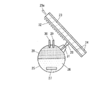
また、図7は上記図4に示した金属化フィルムコンデンサの蒸着電極の酸化や腐食を防止する目的で、表面にオイル保護膜を形成する製造装置のオイル保護膜形成部近傍を拡大した断面図であり、図7において、23aはフィルム23が走行する方向、24は蒸着膜、25はオイルタンク、26はオイル、27は加熱ヒータ、28はオイル蒸気、29は温度センサ、30は圧力センサ、31はノズル、32はオイル保護膜を示し、このようにオイル保護膜形成部は、円筒状のオイルタンク25の内部にオイル26、加熱ヒータ27、温度センサ29および圧力センサ30が収納されているものである。
7 is an enlarged cross-sectional view of the vicinity of an oil protective film forming portion of a manufacturing apparatus for forming an oil protective film on the surface for the purpose of preventing oxidation and corrosion of the vapor deposition electrode of the metalized film capacitor shown in FIG. 7, 23a is a direction in which the
このように構成されたオイル保護膜形成部は、加熱ヒータ27により加熱されたオイル26はオイル蒸気28となりノズル31から噴出し、矢印23aの方向へ走行するフィルム23に設けられた蒸着膜24のノズル側にオイル保護膜32を形成する。なお、温度センサ29と圧力センサ30は、オイルタンク25内部の温度と圧力をモニタリングするものであり、特に圧力センサ30により、長尺のフィルムを金属化する場合であっても、蒸着中のオイル噴出量を一定に保ち、均一なオイル保護膜を形成することができるというものであった(特許文献2)。
しかしながら上記従来の金属化フィルムコンデンサでは、金属化フィルムに設けられたオイル保護膜32が、絶縁マージンを含む金属化フィルムの全面に形成されているために、メタリコンとの密着性が悪く、かつ、漏れ電流が多いという課題があった。
However, in the conventional metallized film capacitor, since the oil
本発明はこのような従来の課題を解決し、メタリコンとの密着性に優れ、かつ、漏れ電流が少ない、優れた性能の金属化フィルムコンデンサを提供することを目的とするものである。 An object of the present invention is to solve such a conventional problem, and to provide a metallized film capacitor having excellent performance with excellent adhesion to a metallicon and low leakage current.
上記課題を解決するために本発明は、誘電体フィルム上に金属蒸着電極を形成した金属化フィルムを一対とし、金属蒸着電極が誘電体フィルムを介して対向するように重ね合わせて巻回した素子と、この素子の両端面に金属溶射によって形成された一対のメタリコン電極からなる金属化フィルムコンデンサにおいて、金属化フィルムとして、誘電体フィルムの幅方向の一端側に非金属蒸着部からなる絶縁マージンを長手方向に連続して設け、この絶縁マージンを除く部分に金属蒸着電極を形成すると共に、金属化フィルムの一端側に設けた絶縁マージンと異なる側の端部に、金属蒸着電極を厚く形成して抵抗値を低くした低抵抗部を設け、絶縁マージンを除いて形成された金属蒸着電極上にオイル保護膜を形成し、低抵抗部上に形成するオイル保護膜の厚みを、低抵抗部を除く金属蒸着電極上に形成されたオイル保護膜の厚さの90%以下とした構成のものである。 The present invention in order to solve the above problems, the dielectric film metallized film forming a metal deposition electrode is a pair on, metals deposition electrode is superposed so as to face via the dielectric film winding And a metallized film capacitor comprising a pair of metallicon electrodes formed by metal spraying on both end faces of the element, as a metallized film, an insulation comprising a non-metal vapor deposition portion on one end side in the width direction of the dielectric film. A margin is continuously provided in the longitudinal direction, and a metal vapor deposition electrode is formed on a portion excluding the insulation margin, and a metal vapor deposition electrode is formed thickly on an end portion different from the insulation margin provided on one end side of the metallized film. to the low resistance section is provided the resistance value was lowered, Oy which forms an oil protective film on the metal deposition electrode formed except insulation margin, it is formed on the low-resistance portion The thickness of the protective film is of a configuration in which more than 90% of the thickness of the oil protective film formed on the metal deposition electrodes except for the low-resistance portion.
以上のように本発明による金属化フィルムコンデンサは、金属化フィルム上に形成したオイル保護膜が絶縁マージン上に形成されていないことにより、金属蒸着電極からメタリコン電極へと流れる電流を低減し、漏れ電流を少なくすることができるという効果が得られるものである。 As described above, the metallized film capacitor according to the present invention reduces the current flowing from the metal vapor deposition electrode to the metallicon electrode because the oil protective film formed on the metallized film is not formed on the insulation margin. The effect that current can be reduced is obtained.
(実施の形態1)
以下、実施の形態1を用いて、本発明の特に請求項1に記載の発明について説明する。
(Embodiment 1)
Hereinafter, the first aspect of the present invention will be described with reference to the first embodiment.
図1は本発明の実施の形態1による金属化フィルムコンデンサの構成を示した断面図であり、図1において、1はポリプロピレンフィルム等からなる誘電体フィルム、2はこの誘電体フィルム1の片面上に一端の絶縁マージン3を除いてアルミニウムの金属を蒸着することにより形成された金属蒸着電極であり、これにより金属化フィルムが形成されているものである。
FIG. 1 is a cross-sectional view showing the configuration of a metallized film capacitor according to
4はこの金属化フィルムに形成された金属蒸着電極2の表面に設けられたオイル保護膜であり、このオイル保護膜4はシリコン系オイル、フッ素系オイル、炭化水素系オイル等を気化させて蒸着することによって形成したものであり、上記金属蒸着電極2を形成するアルミニウムの酸化や腐食を防止して耐湿性を向上させることを目的としており、特に、自動車用に使用されるコンデンサ等のような高抵抗のものは金属蒸着電極2の厚みが薄いために有効なものである。
4 is an oil protective film provided on the surface of the metal
また、上記オイル保護膜4は、絶縁マージン3を除く金属蒸着電極2の表面のみに形成されているものであり、マスク方式等の公知の方法を用いて、上記絶縁マージン3にオイル保護膜4が付着しないようにしているものである。
The oil
そして、このように形成された金属化フィルムを一対とし、上記金属蒸着電極2が誘電体フィルム1を介して対向するように重ね合わせて巻回し、両端面に亜鉛を溶射したメタリコン電極5を形成することによって本実施の形態による金属化フィルムコンデンサが構成されているものである。
Then, the
このように構成された本実施の形態による金属化フィルムコンデンサは、オイル保護膜4を絶縁マージン3上に設けない構成により、金属蒸着電極2からメタリコン電極5へと流れる電流を低減し、漏れ電流を少なくすることができるという格別の効果を奏するものである。すなわち、絶縁マージン3上に誘電体フィルム1よりも抵抗値が低い材料(オイル保護膜等)が存在する場合には、金属蒸着電極2からメタリコン電極5へと流れる電流が増加するために漏れ電流が多くなるものである。
The metallized film capacitor according to the present embodiment configured as described above has a configuration in which the oil
このように構成された本実施の形態による金属化フィルムコンデンサの漏れ電流特性ならびにメタリコン電極との密着性を評価した結果を比較例としての従来品(オイル保護膜が絶縁マージンを含む全面に形成されたもの)と比較して(表1)に示す。 The conventional product (oil protective film is formed on the entire surface including the insulation margin) as a comparative example based on the evaluation results of the leakage current characteristics of the metallized film capacitor and the adhesion to the metallicon electrode according to the present embodiment configured as described above. (Table 1).

(表1)から明らかなように、本実施の形態による金属化フィルムコンデンサは、従来品と比較して漏れ電流特性に優れることが分かるものである。 As is clear from Table 1, it can be seen that the metallized film capacitor according to the present embodiment is superior in leakage current characteristics as compared with the conventional product.
(実施の形態2)
以下、実施の形態2を用いて、本発明の特に請求項2に記載の発明について説明する。
(Embodiment 2)
The second aspect of the present invention will be described below with reference to the second embodiment.
本実施の形態は、上記実施の形態1で図1を用いて説明した金属化フィルムコンデンサに使用される金属化フィルムの構成が一部異なるようにしたものであり、これ以外の構成は実施の形態1と同様であるために同一部分には同一の符号を付与してその詳細な説明は省略し、異なる部分についてのみ以下に図面を用いて詳細に説明する。 In the present embodiment, the structure of the metallized film used in the metallized film capacitor described in the first embodiment with reference to FIG. 1 is partially different. Since it is the same as that of the first embodiment, the same reference numerals are given to the same parts and the detailed description thereof is omitted, and only different parts will be described in detail below with reference to the drawings.
図2は本発明の実施の形態2による金属化フィルムコンデンサの構成を示した断面図、図3は同金属化フィルムコンデンサに使用される金属化フィルムの要部を拡大した断面図であり、図2と図3において、6は金属化フィルムの一端側に設けた絶縁マージン3と異なる側の端部に設けた低抵抗部であり、この低抵抗部6は金属蒸着電極2を厚く形成することによって抵抗値を低くしたものであり、この低抵抗部6は金属蒸着電極2と同様にアルミニウムを用いて形成しても良いし、亜鉛を用いて形成しても良いものである。
FIG. 2 is a cross-sectional view showing a configuration of a metallized film capacitor according to
また、4はオイル保護膜であり、このオイル保護膜4は上記実施の形態1と同様に、絶縁マージン3を除く金属蒸着電極2ならびに低抵抗部6の表面のみに形成されているものであり、かつ、上記低抵抗部6上に形成するオイル保護膜4の厚みt2を、金属蒸着電極2上に形成するオイル保護膜4の厚みt1の90%以下(t2/t1=0.9以下)の厚みになるように形成したものである。
このように構成された本実施の形態による金属化フィルムコンデンサは、低抵抗部6を設けると共に、この低抵抗部6上に形成するオイル保護膜4の厚みを金属蒸着電極2上に形成するオイル保護膜4の厚みの90%以下とした構成により、上記実施の形態1による金属化フィルムコンデンサにより得られる効果に加え、メタリコン電極5を形成する際に密着性を悪化させる要因となるオイル保護膜4が薄いために密着性を向上させることができるという格別の効果を奏するものである。
The metallized film capacitor according to the present embodiment configured as described above is provided with the low resistance portion 6 and the oil for forming the thickness of the oil
このように構成された本実施の形態による金属化フィルムコンデンサの、低抵抗部6上に形成するオイル保護膜4の厚みt2と金属蒸着電極2上に形成するオイル保護膜4の厚みt1の関係(t2/t1)による漏れ電流特性ならびにメタリコン電極との密着性を評価した結果を比較例としての従来品(オイル保護膜が絶縁マージンを含む全面に形成されたもの)と比較して前述の(表1)に示す。
The relationship between the thickness t2 of the oil
(表1)から明らかなように、本実施の形態による金属化フィルムコンデンサは、従来品と比較して漏れ電流特性ならびにメタリコン電極との密着性に優れることが分かるものである。また、低抵抗部6上に形成するオイル保護膜4の厚みt2と金属蒸着電極2上に形成するオイル保護膜4の厚みt1の関係(t2/t1)については90%以下の範囲内が好ましく、これより大きいとメタリコン電極との密着性が少し悪くなり(実施の形態1と同程度)、また逆に小さくなるとオイル保護膜としての機能が低下して耐湿性が悪化するために好ましくないことから、90〜50%の範囲が適していると言えるものである。
As is clear from Table 1, it can be seen that the metallized film capacitor according to the present embodiment is superior in leakage current characteristics and adhesion to the metallicon electrode as compared with the conventional product. Further, the relationship (t2 / t1) between the thickness t2 of the oil
なお、本実施の形態においては、上記低抵抗部6上に形成したオイル保護膜4の厚みは均一な厚みで形成した例を用いて説明したが、本発明はこれに限定されるものではなく、少なくともメタリコン電極5と接続される部分のオイル保護膜4の厚みt2が金属蒸着電極2上に形成されるオイル保護膜4の厚みt1の90%以下の範囲内であれば良いものであり、このメタリコン電極5と接続される部分以外のオイル保護膜4の厚みt2を金属蒸着電極2上に形成されるオイル保護膜4の厚みt1と同等とすることにより、耐湿性の向上を図ることができるようになるものである。
In the present embodiment, the oil
本発明による金属化フィルムコンデンサは、漏れ電流が少なく、かつ、メタリコン電極との密着性に優れるという効果を有し、特に高い信頼性が要求される自動車用のコンデンサ等として有用である。 The metallized film capacitor according to the present invention has an effect that the leakage current is small and the adhesiveness with the metallicon electrode is excellent, and it is useful as a capacitor for automobiles particularly requiring high reliability.
1 誘電体フィルム
2 金属蒸着電極
3 絶縁マージン
4 オイル保護膜
5 メタリコン電極
6 低抵抗部
DESCRIPTION OF
Claims (1)
Priority Applications (1)
| Application Number | Priority Date | Filing Date | Title |
|---|---|---|---|
| JP2008047045A JP4973543B2 (en) | 2008-02-28 | 2008-02-28 | Metallized film capacitors |
Applications Claiming Priority (1)
| Application Number | Priority Date | Filing Date | Title |
|---|---|---|---|
| JP2008047045A JP4973543B2 (en) | 2008-02-28 | 2008-02-28 | Metallized film capacitors |
Publications (3)
| Publication Number | Publication Date |
|---|---|
| JP2009206296A JP2009206296A (en) | 2009-09-10 |
| JP2009206296A5 JP2009206296A5 (en) | 2011-04-14 |
| JP4973543B2 true JP4973543B2 (en) | 2012-07-11 |
Family
ID=41148273
Family Applications (1)
| Application Number | Title | Priority Date | Filing Date |
|---|---|---|---|
| JP2008047045A Active JP4973543B2 (en) | 2008-02-28 | 2008-02-28 | Metallized film capacitors |
Country Status (1)
| Country | Link |
|---|---|
| JP (1) | JP4973543B2 (en) |
Families Citing this family (5)
| Publication number | Priority date | Publication date | Assignee | Title |
|---|---|---|---|---|
| JP5526931B2 (en) * | 2010-03-30 | 2014-06-18 | パナソニック株式会社 | Deposition wire rod and metallized film capacitor formed using the same |
| CN106783170B (en) | 2011-11-11 | 2018-08-24 | 松下知识产权经营株式会社 | Thin film capacitor |
| CN103578751A (en) * | 2013-10-15 | 2014-02-12 | 铜陵其利电子材料有限公司 | Small-width metallized plating membrane for capacitor |
| CN103578750A (en) * | 2013-10-15 | 2014-02-12 | 铜陵其利电子材料有限公司 | Wavy metallized plating film for capacitor |
| CN103578746A (en) * | 2013-10-15 | 2014-02-12 | 铜陵其利电子材料有限公司 | Compound safe anti-explosion metallized film for capacitor |
Family Cites Families (6)
| Publication number | Priority date | Publication date | Assignee | Title |
|---|---|---|---|---|
| JP3874138B2 (en) * | 1997-12-24 | 2007-01-31 | 日立エーアイシー株式会社 | Capacitor and metallized dielectric for capacitor |
| JP3767505B2 (en) * | 2002-03-29 | 2006-04-19 | 松下電器産業株式会社 | Metallized film capacitor, manufacturing method and manufacturing apparatus thereof |
| JP2004095606A (en) * | 2002-08-29 | 2004-03-25 | Matsushita Electric Ind Co Ltd | Method of manufacturing metallized film capacitor, and metallized film capacitor manufactured by the same |
| JP2006264317A (en) * | 2005-02-22 | 2006-10-05 | Toray Ind Inc | Metalized film, film for capacitor and film capacitor using it |
| JP4652163B2 (en) * | 2005-07-20 | 2011-03-16 | 富士通株式会社 | Magnetic recording medium, head slider and magnetic recording apparatus |
| JP2007080907A (en) * | 2005-09-12 | 2007-03-29 | Matsushita Electric Ind Co Ltd | Metallization film capacitor and its manufacturing method |
-
2008
- 2008-02-28 JP JP2008047045A patent/JP4973543B2/en active Active
Also Published As
| Publication number | Publication date |
|---|---|
| JP2009206296A (en) | 2009-09-10 |
Similar Documents
| Publication | Publication Date | Title |
|---|---|---|
| JP5131193B2 (en) | Metallized film capacitors | |
| JP4561832B2 (en) | Metalized film capacitors and inverter smoothing capacitors for automobiles | |
| JP5370363B2 (en) | Metallized film capacitors | |
| JP2004134561A (en) | Metallized film capacitor, smoothing capacitor for inverter using the same, and capacitor for automobile | |
| JP6277436B2 (en) | Film capacitor | |
| JP5012524B2 (en) | Metallized film capacitors | |
| JP3870932B2 (en) | Metallized film capacitors | |
| JP4973543B2 (en) | Metallized film capacitors | |
| JP6167306B2 (en) | Metallized film capacitors | |
| JP2009088258A (en) | Metallized film capacitor | |
| JP4487818B2 (en) | Metallized film capacitors | |
| JP5012515B2 (en) | Metallized film capacitors | |
| JP4915947B2 (en) | Metallized film capacitors | |
| JP2015201527A (en) | Metalized film capacitor | |
| JP5092795B2 (en) | Metallized film capacitors | |
| JP5228591B2 (en) | Metallized film capacitors | |
| JP2010062411A (en) | Metalized film capacitor | |
| JP4893399B2 (en) | Metallized film capacitors | |
| JP2010062410A (en) | Metalized film capacitor | |
| JP5903659B2 (en) | Metallized film capacitor and method for producing metallized film capacitor | |
| JP5934881B2 (en) | Metallized film capacitors | |
| JP5824654B2 (en) | Metallized film capacitors | |
| JP5903648B2 (en) | Metallized film capacitors | |
| JP2008078168A (en) | Metallization film capacitor | |
| JP2008141031A (en) | Metallized film capacitor |
Legal Events
| Date | Code | Title | Description |
|---|---|---|---|
| A521 | Written amendment |
Free format text: JAPANESE INTERMEDIATE CODE: A523 Effective date: 20110225 |
|
| A621 | Written request for application examination |
Free format text: JAPANESE INTERMEDIATE CODE: A621 Effective date: 20110225 |
|
| RD01 | Notification of change of attorney |
Free format text: JAPANESE INTERMEDIATE CODE: A7421 Effective date: 20110314 |
|
| TRDD | Decision of grant or rejection written | ||
| A01 | Written decision to grant a patent or to grant a registration (utility model) |
Free format text: JAPANESE INTERMEDIATE CODE: A01 Effective date: 20120313 |
|
| A01 | Written decision to grant a patent or to grant a registration (utility model) |
Free format text: JAPANESE INTERMEDIATE CODE: A01 |
|
| A61 | First payment of annual fees (during grant procedure) |
Free format text: JAPANESE INTERMEDIATE CODE: A61 Effective date: 20120326 |
|
| R151 | Written notification of patent or utility model registration |
Ref document number: 4973543 Country of ref document: JP Free format text: JAPANESE INTERMEDIATE CODE: R151 |
|
| FPAY | Renewal fee payment (event date is renewal date of database) |
Free format text: PAYMENT UNTIL: 20150420 Year of fee payment: 3 |