JP4950488B2 - Optical deflector, optical deflector manufacturing method, optical scanning device, and image forming apparatus - Google Patents
Optical deflector, optical deflector manufacturing method, optical scanning device, and image forming apparatus Download PDFInfo
- Publication number
- JP4950488B2 JP4950488B2 JP2005373604A JP2005373604A JP4950488B2 JP 4950488 B2 JP4950488 B2 JP 4950488B2 JP 2005373604 A JP2005373604 A JP 2005373604A JP 2005373604 A JP2005373604 A JP 2005373604A JP 4950488 B2 JP4950488 B2 JP 4950488B2
- Authority
- JP
- Japan
- Prior art keywords
- optical
- optical deflector
- mirror
- scanning
- light
- Prior art date
- Legal status (The legal status is an assumption and is not a legal conclusion. Google has not performed a legal analysis and makes no representation as to the accuracy of the status listed.)
- Expired - Fee Related
Links
Images


Classifications
-
- G—PHYSICS
- G02—OPTICS
- G02B—OPTICAL ELEMENTS, SYSTEMS OR APPARATUS
- G02B26/00—Optical devices or arrangements for the control of light using movable or deformable optical elements
- G02B26/08—Optical devices or arrangements for the control of light using movable or deformable optical elements for controlling the direction of light
- G02B26/10—Scanning systems
- G02B26/12—Scanning systems using multifaceted mirrors
- G02B26/121—Mechanical drive devices for polygonal mirrors
Landscapes
- Physics & Mathematics (AREA)
- General Physics & Mathematics (AREA)
- Optics & Photonics (AREA)
- Laser Beam Printer (AREA)
- Mechanical Optical Scanning Systems (AREA)
- Facsimile Scanning Arrangements (AREA)
- Exposure Or Original Feeding In Electrophotography (AREA)
Description
本発明は、光偏向器、光偏向器の製造方法、光走査装置、及び画像形成装置に関し、特に、カラー画像形成装置等に用いられる光偏向器、光偏向器の製造方法、光走査装置、及び画像形成装置に関する。 The present invention relates to an optical deflector, an optical deflector manufacturing method, an optical scanning apparatus, and an image forming apparatus, and more particularly, an optical deflector used in a color image forming apparatus, an optical deflector manufacturing method, an optical scanning apparatus, And an image forming apparatus.
光プリンタ、デジタル複写機、普通ファックス等で用いられる電子写真プロセスを利用した画像形成装置において、カラー化や高速化が進み、光導電性感光体を複数(通常は4個)用いるタンデム方式の画像形成装置が普及してきている。 In image forming apparatuses using an electrophotographic process used in optical printers, digital copying machines, ordinary fax machines, etc., colorization and speeding-up have progressed, and tandem type images using a plurality (usually four) of photoconductive photoreceptors. Forming devices are becoming popular.
特許文献1では、カラー画像形成装置に用いられる光偏向器として、回転軸方向に複数の多面鏡が積層され、各段の多面鏡の偏向反射面が回転方向へ所定角ずれて固定された光偏向器が開示されている。このカラー画像形成装置は、光走査装置の光源数を減らしながらも、高速な画像出力が可能であり、画像形成装置として、省資源、低コスト化が可能である。また、光源数を減らすことで、光源の故障確率も低くできるため、画像形成装置として、信頼性も高めることができる。
しかし、上記の発明は以下の問題を有している。 However, the above invention has the following problems.
従来の光偏向器においては、一体化した状態で複数の偏向反射面を加工する具体的な達成手段が無かったため、偏向反射面が別々に形成された2つの多面鏡を積み重ねて組立てることでポリゴンスキャナを構成していた。この場合、偏向反射面を傷つけることなく、積層された多面鏡の位置を回転方向へ所定角ずらして精度良く固定することが難しかった。さらに、加わる熱ストレスや起動停止の加速・減速動作により、使用時間の経過とともに多面鏡が初期の固定位置からずれて回転体のバランスが崩れ、回転振動が大きくなるという問題があった。 In the conventional optical deflector, since there was no specific means for processing a plurality of deflecting reflecting surfaces in an integrated state, a polygon can be obtained by stacking and assembling two polygon mirrors each having a deflecting reflecting surface formed separately. Configured the scanner. In this case, it has been difficult to accurately fix the position of the stacked polygon mirrors by shifting the position of the stacked polygon mirrors by a predetermined angle in the rotation direction without damaging the deflecting reflection surface. Furthermore, due to the applied thermal stress and start / stop acceleration / deceleration operations, the polygon mirror deviates from the initial fixed position as the usage time elapses, resulting in a problem that the rotating body becomes unbalanced and rotational vibration increases.
本発明は、多面鏡が固定された回転体が、軸受により支持され、モータにより回転駆動される光偏光器において、前記多面鏡が回転軸方向に積層され、かつ前記各多面鏡の反射面が回転方向へ所定角ずれて固定され、前記積層されて一体化した多面鏡の反射面の光偏向に使用される有効領域が、前記各多面鏡の回転軸方向に偏って形成することにより、積層された多面鏡を精度良く所定角度で形成し、加わる熱ストレスや起動停止の加速・減速動作により、使用時間経過とともに多面鏡が初期の固定位置からずれて回転体のバランスが崩れるようなことがなく、回転振動を低減し、省資源、高信頼、低コストな光偏向器、光偏向器の製造方法、光走査装置、及び画像形成装置を提案することを目的としている。 The present invention provides an optical polarizer in which a rotating body to which a polygon mirror is fixed is supported by a bearing and is driven to rotate by a motor, the polygon mirrors are stacked in the direction of the rotation axis, and the reflecting surfaces of the polygon mirrors are The effective area used for light deflection of the reflection surface of the multi-faced mirror that is laminated and integrated is fixed at a predetermined angle in the rotation direction, and is formed by being biased in the direction of the rotation axis of each multi-face mirror. The formed polygonal mirror is accurately formed at a predetermined angle, and due to the applied thermal stress and start / stop acceleration / deceleration operations, the polygonal mirror may deviate from the initial fixed position as the usage time elapses and the balance of the rotating body may be lost. The object of the present invention is to propose an optical deflector, a manufacturing method of an optical deflector, an optical scanning device, and an image forming apparatus that reduce rotational vibration and save resources, high reliability, and low cost.
請求項1記載の発明は、多面鏡が固定された回転体が、軸受により支持され、モータにより回転駆動される光偏向器において、前記多面鏡が回転軸方向に積層され、かつ前記各多面鏡の偏向反射面が回転方向へ所定角ずれて固定され、前記多面鏡の各偏向反射面に鏡面切削加工の軌跡である円弧状の境界線を備え、該境界線は鏡面加工されて光偏向に使用される有効領域と鏡面加工されていない非有効領域との境界線であり、回転軸方向の上側の前記偏向反射面の有効領域は回転軸方向の上側に、回転軸方向の下側の前記偏向反射面の有効領域は回転軸方向の下側に偏って構成されていることを特徴とする。
The invention according to
請求項2記載の発明は、請求項1記載の光偏向器において、前記各多面鏡は別個に構成され、かつ前記回転体を構成する軸に焼きばめされて一体化されていることを特徴とする。 According to a second aspect of the invention, in one SL placement of the optical deflector according to claim, said each polygon mirror are integrated separately constructed, and are shrunk to an axis constituting the rotary body Features.
請求項3記載の発明は、請求項1記載の光偏向器において、前記各多面鏡が一部品として構成されていることを特徴とする。 According to a third aspect of the invention, in one SL placement of the optical deflector according to claim, wherein each polygon mirror, characterized in that it is configured in one piece.
請求項4記載の発明は、請求項3記載の光偏向器において、前記多面鏡の形状が鍛造加工により形成されていることを特徴とする。 According to a fourth aspect of the present invention, in the optical deflector according to the third aspect , the shape of the polygonal mirror is formed by forging.
請求項5記載の発明は、請求項1から4のいずれか1項記載の光偏向器において、前記多面鏡同士が隣接する反射面の角部が面取りされていることを特徴する。 According to a fifth aspect of the present invention, in the optical deflector according to any one of the first to fourth aspects, a corner portion of a reflection surface adjacent to the polygon mirrors is chamfered.
請求項6記載の発明は、請求項5記載の光偏向器において、前記反射面の角部が面取りされて形成される面が平面であることを特徴とする。 According to a sixth aspect of the present invention, in the optical deflector according to the fifth aspect, the surface formed by chamfering the corners of the reflecting surface is a flat surface.
請求項7記載の発明は、請求項1から6のいずれか1項記載の光偏向器の製造方法であって、前記積層された多面鏡が一体化した状態で、前記反射面の長手方向の鏡面切削加工により、前記反射面を形成することを特徴とする。
The invention according to
請求項8記載の発明は、半導体レーザからのビームを、光偏向器を含む光学系を介して被走査面に導いて光スポットを形成し、前記光偏向器により偏向することにより、前記被走査面に走査線を走査する光走査装置において、前記光偏向器が請求項1から7のいずれか1項記載の光偏向器であることを特徴とする。
According to an eighth aspect of the present invention, a beam from a semiconductor laser is guided to a surface to be scanned through an optical system including an optical deflector to form a light spot, and deflected by the optical deflector. An optical scanning device for scanning a surface with a scanning line, wherein the optical deflector is the optical deflector according to any one of
請求項9記載の発明は、半導体レーザから複数のビームを放射し、光偏向器を含む光学系を介して被走査面へ導いて複数の光スポットを形成し、前記光偏向器により偏向することにより、前記被走査面に複数の走査線を走査する光走査装置において、前記光偏向器が請求項1から7のいずれか1項記載の光偏向器であることを特徴とする。
According to a ninth aspect of the present invention, a plurality of beams are emitted from a semiconductor laser, guided to a surface to be scanned through an optical system including an optical deflector to form a plurality of light spots, and deflected by the optical deflector. Accordingly, in the optical scanning device that scans the scanning surface with a plurality of scanning lines, the optical deflector is the optical deflector according to any one of
請求項10記載の発明は、感光体の感光面を光走査装置によって走査して潜像を形成し、前記潜像を可視化して画像をえる画像形成装置において、前記光走査装置が請求項8又は9記載の光走査装置であることを特徴とする。 According to a tenth aspect of the present invention, in the image forming apparatus for forming a latent image by scanning the photosensitive surface of the photosensitive member with an optical scanning device, and visualizing the latent image to obtain an image, the optical scanning device is the eighth aspect. Or an optical scanning device according to 9 .
本発明は、多面鏡が固定された回転体が、軸受により支持され、モータにより回転駆動される光偏光器において、前記多面鏡が回転軸方向に積層され、かつ前記各多面鏡の反射面が回転方向へ所定角ずれて固定され、前記積層されて一体化した多面鏡の反射面の光偏向に使用される有効領域が、前記各多面鏡の回転軸方向に偏って形成することにより、積層された多面鏡を精度良く所定角度で形成し、加わる熱ストレスや起動停止の加速・減速動作により、使用時間経過とともに多面鏡が初期の固定位置からずれて回転体のバランスが崩れ、回転振動が大きくなることを防止できる。 The present invention provides an optical polarizer in which a rotating body to which a polygon mirror is fixed is supported by a bearing and is driven to rotate by a motor, the polygon mirrors are stacked in the direction of the rotation axis, and the reflecting surfaces of the polygon mirrors are The effective area used for light deflection of the reflection surface of the multi-faced mirror that is laminated and integrated is fixed at a predetermined angle in the rotation direction, and is formed by being biased in the direction of the rotation axis of each multi-face mirror. The formed polygonal mirror is accurately formed at a predetermined angle, and due to the applied thermal stress and start / stop acceleration / deceleration operations, the polygonal mirror deviates from the initial fixed position with the passage of time, and the rotating body becomes unbalanced, causing rotational vibration. It can be prevented from becoming large.
以下、本実施形態に係わる光偏向器、光偏向器の製造方法、光走査装置、及び画像形成装置の構成及び動作について説明する。 Hereinafter, the configuration and operation of the optical deflector, the optical deflector manufacturing method, the optical scanning device, and the image forming apparatus according to the present embodiment will be described.
<第1の実施形態>
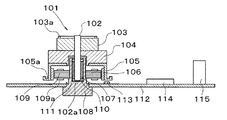
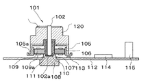
まず、図1及び図2を用いて本実施形態に係わる光偏向器が有する回転体101の構成について説明する。
<First Embodiment>
First, the configuration of the rotating
回転体101は、軸受シャフト102の外周に焼きばめされた多面鏡103、104、多面鏡104に固定されたフランジ105、及びフランジ105に固定されたロータ磁石106を有して構成される。
The rotating
ラジアル軸受は、軸受シャフト102と固定スリーブ107とからなる含油軸受であり、軸受隙間は直径で10μm以下に設定されている。ラジアル軸受は、高速回転での安定性を確保するため、図示しない動圧発生溝を有している。動圧発生溝は、軸受シャフト102の外周面、又は固定スリーブ107の内周面に設けられるが、加工性が良好な焼結部材からなる固定スリーブ107の内周に施すのが好適である。軸受シャフト102の素材としては、焼入れが可能で表面硬度を高くでき、耐磨耗性が良好なマルテンサイト系のステンレス鋼(例えばSUS420J2)が好適である。
The radial bearing is an oil-impregnated bearing including a
フランジ105は、多面鏡104の下部に、かしめ、接着等により固定されている。
The
ロータ磁石106は、フランジ105の下部内面に固定され、軸受ハウジング108に固定されたステータコア109(巻線コイル109a)とともにアウターロータ型のブラシレスモータを構成している。ロータ磁石106は樹脂をバインダーに使用したボンド磁石であり、高速回転時の遠心力による破壊が発生しないように、ロータ磁石106の外径部がフランジ105により保持されている。ロータ磁石106は接着剤により固定しても良いが、圧入固定することにより一層の高速回転、かつ高温環境においても固定部の微移動を生ずることなく、回転体バランスの高精度維持が可能となる。
The
アキシャル方向の軸受は、軸受シャフト102の下端面に形成された凸曲面102aと、その対向面にスラスト受部材110を接触させるピボット軸受である。
The axial bearing is a pivot bearing in which the convex receiving
スラスト受部材110には、樹脂材料等を用い、潤滑性を良好にする。あるいは、スラスト受部材110にマルテンサイト系ステンレス鋼、セラミックス、または金属部材を用い、表面にDLC(ダイヤモンドライクカーボン)処理等の硬化処理を施すことにより、磨耗粉の発生を抑える。
A resin material or the like is used for the
固定スリーブ107とスラスト受部材110とは、軸受ハウジング108に収納され、流体シール111により、油の流出が防止されている。
The fixed sleeve 107 and the
回転体101を25,000rpm以上の高速回転させる場合、振動を小さくするために回転体101のバランスを高精度に修正し、維持しなければならない。回転体101は、アンバランスを修正する部位が上下2ヶ所有し、上側はミラー103に形成された円周凹部103a、下側はフランジ105の円周凹部105aに各々接着剤を塗布することによりバランスを修正する。不釣合い量は10mg・mm以下が必要であり、例えば半径10mmの箇所で修正量は1mg以下に保たれている。
When the rotating
なお、上記のような微少な修正を実行する際に、接着剤等の付着物では管理がしにくい場合や、量が少ないため接着力が弱く40,000rpm以上の高速回転時には剥離、飛散してしまう場合には、回転体の部品の一部を削除する方法(ドリルによる切削やレーザ加工)を実施することが好適である。 When performing such minor corrections as described above, it may be difficult to manage with an adhesive or other adhering material, or it may be peeled off or scattered during high-speed rotation of 40,000 rpm or more because the amount is small and the adhesive strength is weak. In such a case, it is preferable to carry out a method (cutting with a drill or laser processing) for deleting a part of the parts of the rotating body.
本実施形態におけるモータ方式は、径方向に磁気ギャップを有し、ステータコア109の外径部にロータ磁石106がレイアウトされるアウターロータ型といわれる方式である。回転駆動は、ロータ磁石106の磁界により回路基板112に実装されているホール素子113から出力される信号を位置信号として参照し、駆動IC114により巻線コイル109aの励磁切り替えを行い回転する。ロータ磁石106は、径方向に着磁されており、ステータコア109の外周とで回転トルクを発生し回転する。ロータ磁石106の内径以外の外径及び高さ方向は、磁路を開放しており、モータの励磁切り換えのためのホール素子113を開放磁路内に配置している。制御部115は、コネクタを介して不図示のハーネスと接続され、本体からの電力供給、モータの起動停止、回転数等の制御信号の入出力を行う。
The motor system in the present embodiment is a system called an outer rotor type in which a magnetic gap is provided in the radial direction and the
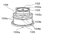
多面鏡(103、104)は、4面の多面鏡が回転軸方向に2個積層され、偏向反射面が回転方向へ45°ずれて、軸受シャフト102に焼きばめされ、一体化されている。多面鏡104は、軸受ハウジング108の上端部と干渉する部分がカップ状に削られている。軸受シャフト102と多面鏡(103、104)は、治具を用いて上下の多面鏡のずれ角度を45°にして、焼きばめすることで固定されている。多面鏡(103、104)は、それぞれの偏向反射面の有効領域(103b、104b)が、回転軸方向(上下方向)に偏って構成されている。すなわち、偏向反射面の上段の有効領域103bは上側に、下段の有効領域104bは下側に偏って構成されている。
The polygon mirrors (103, 104) are formed by laminating two four-sided polygon mirrors in the rotation axis direction, and the deflection reflection surface is shifted by 45 ° in the rotation direction and is shrink-fitted onto the bearing
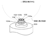
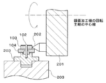
次に、図3及び4を用いて偏向反射面の鏡面加工方法について説明する。図3及び4は、偏向反射面の鏡面加工方法を説明するための正面図及び側面図であり、鏡面切削加工機は主要部のみを模式的に示している。 Next, the mirror surface processing method of the deflection reflection surface will be described with reference to FIGS. 3 and 4 are a front view and a side view for explaining a mirror surface processing method of the deflecting and reflecting surface, and the mirror surface cutting machine schematically shows only the main part.
鏡面切削加工機の回転主軸には円盤状部材201が固定され、円盤状部材201の端面の外周側には鏡面加工用の切削工具202が取り付けられている。鏡面切削加工機は、回転主軸を高速回転させて、偏向反射面の長手方向に切削工具202を通過させることにより、偏向反射面を切削して鏡面を形成する。
A disk-shaped
このとき、鏡面加工機の切削工具202と多面鏡(103、104)の角部分が干渉し、積層された多面鏡の上下の境界部分は鏡面加工することができないため、非有効領域となり、偏向反射面の有効領域は偏って構成されている。すなわち、上側の偏向反射面を加工するときには下側の多面鏡の角部分と切削工具が干渉し、下側の偏向反射面を加工するときには上側の多面鏡の角部分と切削工具が干渉するため、上側の偏向反射面の有効領域103bは上側に、下側の偏向反射面の有効領域104bは下側に偏って構成されている。鏡面加工終了後、偏向反射面には、図2に示すように、鏡面切削加工の軌跡である円弧状の境界(103c、104c)が形成される。
In this case, the corner portion interferes the
多面鏡を鏡面切削加工機に固定する多面鏡固定装置203は、不図示の回転位置決め機構を有し、軸受シャフト102と一体化された多面鏡(103、104)とが固定され、偏向反射面が1面ずつ加工される。具体的には、1面目の加工が終わると、多面鏡固定装置203の回転位置決め機構により多面鏡が所定角度回転され、2面目が加工される。多面鏡が4面の場合は、45°回転させて、上下交互に加工しても良いし、90°回転させて上側4面を続けて加工した後、下側4面を加工するようにしても良い。多面鏡固定装置203の回転位置決め機構は、1′(=1/60°)以下の高い位置決め角度精度があるため、多面鏡のずれ角度を高い精度で形成することができる。
The polygon
上記実施形態に係わる光偏向器では、4面の多面鏡(103、104)が回転軸方向に2個が積層され、偏向反射面が回転方向へ45°ずれて、軸受シャフト102に焼きばめされ、一体化されているので、積層された多面鏡(103、104)が上下で回転方向へ所定角ずれた状態で精度良く形成され、加わる熱ストレスや起動停止の加減速動作により、多面鏡が初期の固定位置からずれて回転体のバランスが崩れ振動が大きくなることがない。また、偏向反射面の有効領域(103b、104b)は、回転軸方向(上下方向)に偏って構成されているので、鏡面加工機の切削工具と多面鏡の角部分が干渉することなく、一体化された状態で偏向反射面を加工することができる。また、多面鏡(103、104)は、簡単な形状であるため、鏡面加工機で偏向反射面を加工する前に、多面鏡と略同一の形状に加工した上で、偏向反射面を生成することができる(以下、ブランク加工とする)。そのため、多面鏡は、ブランク加工が容易で、かつ低コストで作成することができる。なお、本実施形態においては、4面の多面鏡を用いたが、多面鏡の面数は4面に限定されるものではない。例えば、6面の多面鏡を回転軸方向に2個積層させ、偏向反射面を回転方向へ30°ずらして軸受シャフトに焼きばめさせて一体化させてもよい。以下に記載する実施形態においても同様である。
In the optical deflector according to the above-described embodiment, two four-sided mirrors (103, 104) are stacked in the rotation axis direction, and the deflection reflection surface is shifted by 45 ° in the rotation direction, so that the bearing
<第2の実施形態>
まず、図5及び図6を用いて本実施形態に係わる光偏向器が有する回転体101の構成について説明する。
<Second Embodiment>
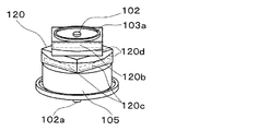
First, the configuration of the
本実施形態に係わる光偏向器の回転体101が有する多面鏡120は、一部品で構成される。なお、本実施形態に係わる光偏向器の回転体101は、多面鏡120の構成のみが異なるため、他の構成については同じ番号を付し説明を省略する。
The
多面鏡120は、4面の多面鏡が回転軸方向に2個積層され、上下の偏向反射面が回転方向へ45°ずれて1部品で構成されている。1部品で構成される多面鏡120は、軸受シャフト102に焼きばめされて、一体化されている。
The
積層された多面鏡120は、それぞれの偏向反射面の有効領域(120b、120c)が、回転軸方向(上下方向)に偏って構成されている。すなわち、上段の有効領域120bは上側に、下段の有効領域120cは下側に、偏向反射面の有効領域が偏って構成されている。
The laminated
偏向反射面の鏡面形成方法は、第1の実施形態と同様であり、鏡面加工終了後、偏向反射面には、図6に示すように、鏡面切削加工の軌跡である円弧状の境界120dが形成される。
The method of forming the mirror surface of the deflecting reflecting surface is the same as that of the first embodiment. After the mirror processing is finished, the deflecting reflecting surface has an arc-shaped
本実施形態によれば、上下の多面鏡が1部品に集約され、部品点数が少なく、焼きばめ時に上下のずれ角度を設定する治具は必要ないため組立が容易である。また、上下の多面鏡が1部品で構成されるため、やや複雑な形状の部品になるが、鍛造加工により形状を形成すれば、素材から切削加工により多面体形状を削りだす場合に比べて、低コストで形成することができる。 According to the present embodiment, the upper and lower polygon mirrors are integrated into one part, the number of parts is small, and a jig for setting the vertical deviation angle at the time of shrink fitting is not necessary, so that assembly is easy. In addition, since the upper and lower polygon mirrors are composed of a single part, it becomes a part with a slightly complicated shape. However, if the shape is formed by forging, it is lower than the case where the polyhedral shape is cut out from the material by cutting. Can be formed at a cost.
<第3の実施形態>
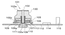
まず、図7及び図8を用いて本実施形態に係わる光偏向器が有する回転体101の構成について説明する。
<Third Embodiment>
First, the configuration of the
本実施形態に係わる光偏向器は、多面鏡130の構成のみが第1及び第2の実施形態に係わる光偏向器と異なるため、他の構成については同じ番号を付し説明を省略する。
Since the optical deflector according to the present embodiment is different from the optical deflector according to the first and second embodiments only in the configuration of the
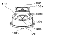
本実施形態の光偏向器の多面鏡130は、多面鏡同士が隣接する偏向反射面の角部が削ぎ落とされて構成されている。この削ぎ落とされた角部は偏向反射面の鏡面加工時に切削工具と干渉する部分である。しかし、本実施形態においては、鏡面加工機の切削工具と干渉する多面鏡の角部分が削られているため、多面鏡同士の隣接境界に近づく方向に、より広く偏向反射面の有効領域(130b、130c)を形成することができる。その結果、偏向反射面の回転軸方向の位置を上下で大きく離す必要が無く、より近づけることができるので、多面鏡130を回転軸方向に小型化できる。さらに、偏向反射面の角部が削ぎ落とされて形成される面を平面とすれば、多面鏡130のブランク加工が容易で低コストである。
The
図9及び図10に示す偏向反射面の鏡面形成方法は、第1及び第2の実施形態と同様である。偏向反射面には、鏡面加工終了後、図7に示すように、鏡面切削加工の軌跡である円弧状の境界130dが形成される。円弧状の境界線130dは、第1及び第2の実施形態よりも上下の偏向反射面同士の隣接境界に接近した位置に形成される。
The mirror surface forming method of the deflecting reflecting surface shown in FIGS. 9 and 10 is the same as in the first and second embodiments. As shown in FIG. 7, an arc-shaped
また、多面鏡130は、第2の実施形態と同様に、鍛造加工により形状を形成することにより、素材から切削加工により多面体形状を削りだす場合に比べて、低コストで形成することができる。
Further, as in the second embodiment, the
<第4の実施形態>
次に、上述の第1から3の実施形態に係わる光偏向器を有する光走査装置の構成及び動作について説明する。
<Fourth Embodiment>
Next, the configuration and operation of the optical scanning device having the optical deflector according to the first to third embodiments will be described.
まず、図11を用いて本実施形態に係わる光走査装置の各部の動作について説明する。 First, the operation of each part of the optical scanning device according to the present embodiment will be described with reference to FIG.
符号1、1’は半導体レーザを示す。半導体レーザ(1、1´)は「1つの光源を構成する2つの発光源」であり、それぞれ1本の光ビームを放射する。これら半導体レーザ(1、1´)は、ホルダ2に所定の位置関係で保持されている。
半導体レーザ(1、1´)から放射された各光ビームは、それぞれカップリングレンズ(3、3´)により以後の光学系に適した光束形態(平行光束あるいは弱い発散性又は弱い収束性の光束)に変換される。本実施形態においては、カップリングレンズ(3、3´)によりカップリングされた光ビームは共に平行光束である。 Each light beam emitted from the semiconductor laser (1, 1 ′) is converted into a light beam form (parallel light beam or weak divergent or weak convergent light beam) suitable for the subsequent optical system by the coupling lens (3, 3 ′). ). In the present embodiment, the light beams coupled by the coupling lenses (3, 3 ′) are both parallel light beams.
カップリングレンズ(3、3´)から射出し、所望の光束形態となった各光ビームは、光ビーム幅を規制するアパーチュア12の開口部を通過して「ビーム整形」されたのち、ハーフミラープリズム4に入射し、ハーフミラープリズム4の作用により副走査方向に2分割されてそれぞれが2本の光ビームに分けられる。
Each light beam emitted from the coupling lens (3, 3 ') and having a desired luminous flux form is "beam-shaped" through the opening of the
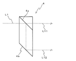
図12にハーフミラープリズム4により光ビームが副走査方向に2分割された様子を示す。なお、図12においては、半導体レーザ1から放射された光ビームL1が、副走査方向に2分割され、光ビーム(L11、L12)となって放出された様子を示しているが、半導体レーザ1´から放射された光ビームL2も同様に分割される。
FIG. 12 shows a state where the light beam is divided into two in the sub-scanning direction by the
図12において、上下方向が副走査方向であり、ハーフミラープリズム4は半透鏡4aと反射面4bとを副走査方向に並列して有する。光ビームL1は、ハーフミラープリズム4に入射すると半透鏡4aに入射し、一部は半透鏡4aを直進的に透過して光ビームL11となり、残りは反射されて反射面4bに入射し、反射面4bにより全反射されて光ビームL12となる。
In FIG. 12, the vertical direction is the sub-scanning direction, and the
この例において、半透鏡4aと反射面4bとは互いに平行であるため、ハーフミラープリズム4から射出する光ビームL11と光ビームL12とは互いに平行である。このように、半導体レーザ1からの光ビームは、2つの光ビームL11、光ビームL12として副走査方向に2分割される。半導体レーザ1´からの光ビームも同様にして2分割される。
In this example, since the half mirror 4a and the reflecting surface 4b are parallel to each other, the light beam L11 and the light beam L12 emitted from the
このように、ハーフミラープリズム4において1つの光源(m=1)から2本の光ビームが放射され、これら2本の光ビームが副走査方向に2分割(q=2)されて4本の光ビームが得られる。
In this way, in the
ハーフミラープリズム4から放射された4本の光ビームは、シリンドリカルレンズ(5a、5b)に入射し、これらシリンドリカルレンズ(5a、5b)の作用により副走査方向へ集光され、多面鏡式光偏向器7の偏向反射面近傍に「主走査方向に長い線像」として結像する。
The four light beams emitted from the
半導体レーザ(1、1´)から放射され、ハーフミラープリズム4より分割された光ビームのうち、ハーフミラープリズム4の半透鏡4aを直進的に透過した光ビーム(図12に示す光ビームL11)がシリンドリカルレンズ5aに入射し、半透鏡4aにより反射され、更に反射面4bで反射された光ビーム(図12に示す光ビームL12)がシリンドリカルレンズ5bに入射する。
Of the light beams emitted from the semiconductor laser (1, 1 ') and divided by the
符号6は多面鏡式光偏向器7の防音ハウジングの窓に設けられた「防音ガラス」を示す。光源側からの4本の光ビームは防音ガラス6を介して多面鏡式光偏向器7に入射し、偏向された光ビームは防音ガラス6を介して走査結像光学系側へ射出する。
多面鏡式光偏向器7は、図示のように上ポリゴンミラー7a、下ポリゴンミラー7bを回転軸方向に上下2段に積層して一体とし、図示されない駆動モータにより回転軸の周りに回転させられるようになっている。
As shown in the figure, the polygon mirror type
上ポリゴンミラー7a及び下ポリゴンミラー7bは、本実施形態において、共に「4面の偏向反射面」を持つ同一形状のものであるが、上ポリゴンミラー7aの偏向反射面に対し、下ポリゴンミラー7bの偏向反射面が、回転方向へ所定角:θ(=45度)ずれている。
In this embodiment, the
符号8a及び8bは「第1走査レンズ」、符号10a及び10bは「第2走査レンズ」、符号9a及び9bは「光路折り曲げミラー」を示している。また、符号11a及び11bは「光導電性感光体」を示している。
第1走査レンズ8aと、第2走査レンズ10aと、光路折り曲げミラー9aとは、多面鏡式光偏向器7の上ポリゴンミラー7aにより偏向される2本の光ビーム(半導体レーザ(1、1´)から放射され、ハーフミラープリズム4の半透鏡4aを透過した2本の光ビーム)を、対応する光走査位置である光導電性感光体11a上に導光して、副走査方向に分離した2つの光スポットを形成する1組の走査結像光学系を構成する。
The
第1走査レンズ8bと、第2走査レンズ10bと、光路折り曲げミラー9bとは、多面鏡式光偏向器7の下ポリゴンミラー7bにより偏向される2本の光ビーム(半導体レーザ(1、1´)から放射され、ハーフミラープリズム4の半透鏡4aにより反射された2本の光ビーム)を、対応する光走査位置である光導電性感光体11b上に導光して、副走査方向に分離した2つの光スポットを形成する1組の走査結像光学系を構成する。
The
半導体レーザ(1、1´)から放射された光ビームは、多面鏡式光偏向器7の回転軸方向から見て「偏向反射面位置の近傍において主光線が交差する」ように光学配置が定められており、従って、偏向反射面に入射してくる2光束の各対は光ビーム相互が「開き角(偏向反射面の側から光源側を見たとき、2本の光ビームの回転軸に直交する面への射影がなす角をいう。)」を有する。
The optical arrangement of the light beam emitted from the semiconductor laser (1, 1 ') is determined so that the principal rays intersect in the vicinity of the position of the deflecting reflecting surface when viewed from the rotational axis direction of the polygon mirror
この「開き角」により、光導電性感光体(11a、11b)のそれぞれに形成される2つの光スポットは主走査方向にも分離しており、このため各感光体を光走査する2本の光ビームを個別的に検出して光走査開始の同期を光ビームごとに取ることができる。 Due to this “open angle”, the two light spots formed on each of the photoconductive photoreceptors (11a, 11b) are also separated in the main scanning direction. It is possible to detect the light beams individually and synchronize the start of optical scanning for each light beam.
このようにして、多面鏡式光偏向器7の上ポリゴンミラー7aにより偏向される2本の光ビームにより、光導電性感光体11aがマルチビーム走査され、多面鏡式光偏向器7の下ポリゴンミラー7bにより偏向される2本の光ビームにより、光導電性感光体11bがマルチビーム走査される。
In this manner, the photoconductive
多面鏡式光偏向器7の上ポリゴンミラー7a及び下ポリゴンミラー7bの偏向反射面は互いに回転方向に45度ずれているので、上ポリゴンミラー7aによる偏向光ビームが光導電性感光体11aの光走査を行うとき、下ポリゴンミラー7bによる偏向光ビームは、光導電性感光体11bには導光されず、下ポリゴンミラー7bによる偏向光ビームが光導電性感光体11bの光走査を行うとき、上ポリゴンミラー7aによる偏向光ビームは、光導電性感光体11aには導光されない。
Since the deflecting and reflecting surfaces of the
即ち、光導電性感光体(11a、11b)の光走査は「時間的にずれて交互」に行われることになる。図13は、この状況を説明する図である。なお、図13において、多面鏡式光偏向器へ入射する光ビーム(実際には4本である)を「入射光」、偏向される光ビームを「偏向光a、偏向光b」として示している。 That is, the optical scanning of the photoconductive photoconductors (11a, 11b) is performed "alternatingly shifted in time". FIG. 13 is a diagram for explaining this situation. In FIG. 13, the light beams incident on the polygon mirror optical deflector (actually four beams) are indicated as “incident light”, and the deflected light beams are indicated as “deflected light a and deflected light b”. Yes.
図13(a)は、入射光が多面鏡式光偏向器7に入射し、上ポリゴンミラー7aで反射されて偏向された「偏向光a」が光走査位置へ導光されるときの状況を示している。このとき、下ポリゴンミラー7bによる偏向光bは光走査位置へは向かわない。図13(b)は、下ポリゴンミラー7bで反射されて偏向された「偏向光b」が光走査位置へ導光されるときの状況を示している。このとき、上ポリゴンミラー7aによる偏向光aは光走査位置へは向かわない。
FIG. 13A shows the situation when incident light enters the polygon mirror
なお、一方のポリゴンミラーによる偏向光が光走査位置へ導光されている間に、他方のポリゴンミラーによる偏向光が「ゴースト光」として作用しないように、図13に如き適宜の遮光手段SDを用いて、光走査位置へ導光されない偏向光を遮光するのがよい。これは実際には、前述の「防音ハウジング」の内壁を非反射性とすることにより容易に実現できる。 In order to prevent the deflected light from the other polygon mirror from acting as “ghost light” while the deflected light from one polygon mirror is guided to the optical scanning position, an appropriate light shielding means SD as shown in FIG. It is preferable to shield the deflected light that is not guided to the optical scanning position. In practice, this can be easily realized by making the inner wall of the “soundproof housing” non-reflective.
上述したように、光導電性感光体(11a、11b)による(マルチビーム方式の)光走査は交互に行われるので、例えば、光導電性感光体11aの光走査が行われるときは光源の光強度を「黒画像の画像信号」で変調し、光導電性感光体11bの光走査が行われるときは光源の光強度を「マゼンタ画像の画像信号」で変調すれば、光導電性感光体11aには黒画像の静電潜像を、光導電性感光体11bにはマゼンタ画像の静電潜像を書込むことができる。
As described above, since the (multi-beam) light scanning by the photoconductive photoconductors (11a, 11b) is performed alternately, for example, when the
図14は「共通の光源(半導体レーザ1、1´)」により黒画像及びマゼンタ画像の書込みを行う場合において、「有効走査領域において全点灯する場合」のタイムチャートを示している。実線は黒画像の書込みに相当する部分、破線はマゼンタ画像の書込みに相当する部分を示す。黒画像及びマゼンタマゼンタ画像の書き出しのタイミングは、前述の如く、有効走査領域外に配備される同期受光手段(一般に、図示しないフォトダイオードである。)で光走査開始位置へ向かう光ビームを検知することにより決定される。
FIG. 14 shows a time chart of “when all the light is turned on in the effective scanning area” when writing a black image and a magenta image by the “common light source (
本実施形態に係わる光走査装置によれば、光源部の部品点数、材料が削減されて、環境負荷が低減され、光源の故障確率も低く抑えることができる。 According to the optical scanning device according to the present embodiment, the number of parts and materials of the light source unit are reduced, the environmental load is reduced, and the failure probability of the light source can be kept low.
<第5の実施形態>
次に、上述の第1から3の実施形態に係わる光偏向器を有する画像形成装置の構成及び動作について説明する。
<Fifth Embodiment>
Next, the configuration and operation of the image forming apparatus having the optical deflector according to the first to third embodiments will be described.
まず、図15を用いて本実施形態に係わる画像形成装置が有する光走査装置の各部の動作について説明する。 First, the operation of each part of the optical scanning device included in the image forming apparatus according to the present embodiment will be described with reference to FIG.
図15は、光走査装置の光学系部分を、副走査方向、即ち、多面鏡式光偏向器7の回転軸方向から見た図である。図示の簡略化のため、多面鏡式光偏向器7から光走査位置に至る光路上の光路屈曲用ミラーの図示を省略し、光路を直線として描いた。
FIG. 15 is a view of the optical system portion of the optical scanning device as viewed from the sub-scanning direction, that is, the rotation axis direction of the polygon mirror type
本実施形態は、2個の光源からn(=4)個の光走査位置へ向かう光走査光路を形成し、4個の光走査位置への光走査光路を時間的にずらして順次に選択し、選択された光走査光路により光走査される光走査位置に応じた画像信号により2個の光源からの光ビームを強度変調することにより、2個の光源からの光ビームでn個の光走査位置を光走査する光走査装置において、p(=1)本の光ビームを放射するm(=2)個の光源と、各光源からの各光ビームを副走査方向にq(=2)分割して、4つの光走査位置をそれぞれ1本の光ビームで光走査する。 In the present embodiment, optical scanning optical paths from two light sources to n (= 4) optical scanning positions are formed, and the optical scanning optical paths to the four optical scanning positions are sequentially selected while being shifted in time. The light beams from the two light sources are intensity-modulated by the image signal corresponding to the optical scanning position that is optically scanned by the selected optical scanning optical path, so that n light scans are performed by the light beams from the two light sources. In an optical scanning device that optically scans a position, m (= 2) light sources that emit p (= 1) light beams, and each light beam from each light source is divided into q (= 2) in the sub-scanning direction. Then, each of the four optical scanning positions is optically scanned with one light beam.
また、個々の光走査位置には、光導電性感光体(11Y、11M、11C、11K)が配置され、これら4個の光導電性感光体に形成される静電潜像をマゼンタ、イエロー、シアン、黒のトナーにより個別に可視化し、カラー画像を形成する。図15において、符号1YM、1CKはそれぞれ半導体レーザを示す。これら半導体レーザ(1YM、1CK)は、それぞれが1本の光ビームを放射する。半導体レーザ1YMは「イエロー画像に対応する画像信号」と「マゼンタ画像に対応する画像信号」で交互に強度変調される。半導体レーザ1CKは「シアン画像に対応する画像信号」と「黒画像に対応する画像信号」で交互に強度変調される。 In addition, photoconductive photoconductors (11Y, 11M, 11C, and 11K) are arranged at the respective optical scanning positions, and electrostatic latent images formed on these four photoconductive photoconductors are magenta, yellow, Visualized separately with cyan and black toners to form a color image. In FIG. 15, reference numerals 1YM and 1CK denote semiconductor lasers, respectively. Each of these semiconductor lasers (1YM, 1CK) emits one light beam. The intensity of the semiconductor laser 1YM is alternately modulated with “an image signal corresponding to a yellow image” and “an image signal corresponding to a magenta image”. The intensity of the semiconductor laser 1CK is alternately modulated with “an image signal corresponding to a cyan image” and “an image signal corresponding to a black image”.
半導体レーザ1YMから放射された光ビームはカップリングレンズ3YMにより平行光束化され、アパーチュア12YMを通過してビーム整形されたのち、ハーフミラープリズム4YMに入射して、副走査方向に分離した2本の光ビームにビーム分割される。ハーフミラープリズム4YMは、図12に即して説明したハーフミラープリズム4と同様のものである。分割された光ビームの1本はイエロー画像を書込むのに使用され、他の1本はマゼンタ画像を書込むのに使用される。
The light beam emitted from the semiconductor laser 1YM is converted into a parallel beam by the coupling lens 3YM, and after passing through the aperture 12YM, the beam is shaped, and then incident on the half mirror prism 4YM and separated in the sub-scanning direction. Beam split into light beams. The half mirror prism 4YM is the same as the
副走査方向に分割された2本の光ビームは、副走査方向に配列されたシリンドリカルレンズ5Y、5M(副走査方向に重なり合うように配置されている。)により、それぞれ副走査方向へ集光され、多面鏡式光偏向器7に入射する。多面鏡式光偏向器7は、図11及び図13に即して説明したものと同様のものであり、4面の偏向反射面を持つポリゴンミラーを回転軸方向へ2段に積層し、ポリゴンミラー相互の偏向反射面を回転方向へずらして一体化したものである。シリンドリカルレンズ(5Y、5M)による主走査方向に長い線像は、各ポリゴンの偏向反射面位置近傍に結像する。
The two light beams divided in the sub-scanning direction are condensed in the sub-scanning direction by
多面鏡式光偏向器7により偏向される光ビームは、それぞれ第1走査レンズ(8Y、8M)、第2走査レンズ(10Y、10M)を透過し、これらレンズの作用により光走査位置(11Y、11M)に光スポットを形成し、これら光走査位置を光走査する。
The light beams deflected by the polygon mirror
同様に、半導体レーザ1CKから放射された光ビームはカップリングレンズ3CKにより平行光束化され、アパーチュア12CKを通過してビーム整形されたのち、ハーフミラープリズム4CKにより、副走査方向に分離した2本の光ビームにビーム分割される。ハーフミラープリズム4CKは、ハーフミラープリズム4YMと同様のものである。分割された光ビームの1本はシアン画像を書込むのに使用され、他の1本は黒画像を書込むのに使用される。 Similarly, the light beam radiated from the semiconductor laser 1CK is converted into a parallel beam by the coupling lens 3CK, shaped through the aperture 12CK, and then separated into two in the sub-scanning direction by the half mirror prism 4CK. Beam split into light beams. The half mirror prism 4CK is the same as the half mirror prism 4YM. One of the split light beams is used to write a cyan image and the other one is used to write a black image.
副走査方向に分割された2本の光ビームは、副走査方向に配列されたシリンドリカルレンズ5C、5K(副走査方向に重なり合うように配置されている。)によりそれぞれ、副走査方向へ集光され、多面鏡式光偏向器7に入射して偏向され、それぞれ第1走査レンズ8C、8K、第2走査レンズ10C、10Kを透過し、これらレンズの作用により光走査位置11C、11Kに光スポットを形成し、これら光走査位置を光走査する。
The two light beams divided in the sub-scanning direction are condensed in the sub-scanning direction by the
次に、図15に示す光走査装置を有する画像形成装置の構成及び動作について図16を用いて説明する。なお、図16において、符号20で示す部分が光走査装置で、図15に即して説明した部分である。
Next, the configuration and operation of the image forming apparatus having the optical scanning device shown in FIG. 15 will be described with reference to FIG. In FIG. 16, the portion indicated by
図16に示すように、多面鏡式光偏向器7の上段のポリゴンミラーにより偏向される光ビームのうち一方は、光路折り曲げミラーmM1、mM2、mM3により屈曲された光路により光走査位置の実体をなす光導電性感光体11Mに導光され、他方の光ビームは、光路折り曲げミラーmC1、mC2、mC3により屈曲された光路により光走査位置の実体をなす光導電性感光体11Cに導光される。
As shown in FIG. 16, one of the light beams deflected by the upper polygon mirror of the polygon mirror
また、多面鏡式光偏向器7の下段のポリゴンミラーにより偏向される光ビームのうち一方は、光路折り曲げミラーmYにより屈曲された光路により光走査位置の実体をなす光導電性感光体11Yに導光され、他方の光ビームは、光路折り曲げミラーmKにより屈曲された光路により光走査位置の実体をなす光導電性感光体11Kに導光される。
In addition, one of the light beams deflected by the lower polygon mirror of the polygon mirror type
従って、m(=2)個の半導体レーザ(1YM、1CK)からの光ビームがそれぞれハーフミラープリズム(4YM、4CK)で2本の光ビームに分割されて4本の光ビームとなり、これら4本の光ビームにより、4個の光導電性感光体(11Y、11M、11C、11K)が光走査される。光導電性感光体11Yと11Mとは半導体レーザ1YMからの光ビームが2分割された各光ビームにより、多面鏡式光偏向器7の回転に伴い交互に光走査され、光導電性感光体11Cと11Kとは半導体レーザ1CKからの光ビームが2分割された各光ビームにより、多面鏡式光偏向器7の回転に伴い交互に光走査される。
Accordingly, the light beams from m (= 2) semiconductor lasers (1YM, 1CK) are divided into two light beams by the half mirror prisms (4YM, 4CK), respectively, resulting in four light beams. The four photoconductive photosensitive members (11Y, 11M, 11C, and 11K) are optically scanned by the light beam. The
光導電性感光体(11Y〜11K)は、何れも時計回りに等速回転され、帯電手段をなす帯電ローラ(TY、TM、TC、TK)により均一帯電され、それぞれ対応する光ビームの光走査を受けてイエロー、マゼンタ、シアン、黒の各色画像を書込まれ対応する静電潜像(ネガ潜像)が形成される。 Each of the photoconductive photoreceptors (11Y to 11K) is rotated at a constant speed in the clockwise direction, and is uniformly charged by charging rollers (TY, TM, TC, TK) serving as charging means, and each of the corresponding light beams is scanned with light. In response, yellow, magenta, cyan, and black color images are written to form corresponding electrostatic latent images (negative latent images).
これら静電潜像はそれぞれ現像装置(GY、GM、GC、GK)により反転現像され、光導電性感光体(11Y、11M、11C、11K)上にそれぞれイエロートナー画像、マゼンタトナー画像、シアントナー画像、黒トナー画像が形成される。 These electrostatic latent images are respectively developed by reversal by developing devices (GY, GM, GC, GK), and yellow toner images, magenta toner images, cyan toners are respectively formed on the photoconductive photoreceptors (11Y, 11M, 11C, 11K). An image and a black toner image are formed.
これら各色トナー画像は、図示されない「転写シート」上に転写される。即ち、転写シートは搬送ベルト17により搬送され、転写器15Yにより光導電性感光体11Y上からイエロートナー画像が転写され、転写器(15M、15C、15K)によりそれぞれ、光導電性感光体(11M、11C、11K)から、マゼンタトナー画像、シアントナー画像、黒トナー画像を順次に転写される。
These color toner images are transferred onto a “transfer sheet” (not shown). That is, the transfer sheet is conveyed by the conveying
このようにして転写シート上においてイエロートナー画像〜黒トナー画像が重ね合わせられてカラー画像を合成的に構成する。このカラー画像は定着装置19により転写シート上に定着されてカラー画像が得られる。
In this way, a yellow toner image to a black toner image are superimposed on the transfer sheet to compose a color image synthetically. This color image is fixed on the transfer sheet by the fixing
即ち、本実施形態は、複数の光導電性感光体に光走査により個別的に静電潜像を形成し、これら静電潜像を可視化してトナー画像とし、得られるトナー画像を同一のシート状記録媒体上に転写して合成的に画像形成を行うタンデム式の画像形成装置において、光導電性感光体の数が4であり、光走査装置として、2個の光源(1YM、1CK)を用いて、各光源からの光ビームがそれぞれ2個の光導電性感光体を光走査するように構成され、4個の光導電性感光体(11M、11Y、11C、11K)に形成される静電潜像をマゼンタ、イエロー、シアン、黒のトナーで個別に可視化し、カラー画像を形成することにより、光源部の部品点数、材料が削減されて、環境負荷が低減され、光源の故障確率も低く抑え、かつ環境負荷が低減された画像形成装置を提供することができる。 That is, in the present embodiment, an electrostatic latent image is individually formed on a plurality of photoconductive photosensitive members by optical scanning, the electrostatic latent images are visualized to form a toner image, and the obtained toner image is the same sheet. In a tandem type image forming apparatus that transfers images onto a recording medium and forms images synthetically, the number of photoconductive photoconductors is 4, and two light sources (1YM, 1CK) are used as an optical scanning device. And light beams from each light source are configured to optically scan two photoconductive photoreceptors, respectively, and are formed on four photoconductive photoreceptors (11M, 11Y, 11C, and 11K). The electrostatic latent image is individually visualized with magenta, yellow, cyan, and black toners, and a color image is formed, thereby reducing the number of parts and materials in the light source, reducing the environmental burden, and reducing the failure probability of the light source. Low environmental burden It is possible to provide an image forming apparatus.
なお、上述の画像形成装置では、各光導電性感光体の光走査を「シングルビーム方式」で行っているが、各光源側を図11の如くに構成し、光導電性感光体の光走査を「マルチビーム方式」で行うようにできることは当然である。 In the above-described image forming apparatus, the light scanning of each photoconductive photoconductor is performed by the “single beam method”, but each light source side is configured as shown in FIG. Of course, the “multi-beam method” can be performed.
1、1´ 半導体レーザ
3、3´ カップリングレンズ
4 ハーフミラープリズム
5、5´ シリンドリカルレンズ
6 防音ガラス
7 多面鏡式光偏向器
7a 上ポリゴンミラー
7b 下ポリゴンミラー
8a、8b 第1走査レンズ
10a、10b 第2走査レンズ2
11a、11b 光導電性感光体
DESCRIPTION OF
11a, 11b Photoconductive photoreceptor
Claims (10)
前記多面鏡が回転軸方向に積層され、かつ前記各多面鏡の偏向反射面が回転方向へ所定角ずれて固定され、前記多面鏡の各偏向反射面に鏡面切削加工の軌跡である円弧状の境界線を備え、
該境界線は鏡面加工されて光偏向に使用される有効領域と鏡面加工されていない非有効領域との境界線であり、
回転軸方向の上側の前記偏向反射面の有効領域は回転軸方向の上側に、回転軸方向の下側の前記偏向反射面の有効領域は回転軸方向の下側に偏って構成されていることを特徴とする光偏向器。 In an optical deflector in which a rotating body to which a polygon mirror is fixed is supported by a bearing and is driven to rotate by a motor.
The polygon mirrors are stacked in the direction of the rotation axis, and the deflection reflection surfaces of the polygon mirrors are fixed at a predetermined angle in the rotation direction, and arc-shaped as a locus of mirror cutting on the deflection reflection surfaces of the polygon mirrors . With a border,
The boundary line is a boundary line between an effective area that is mirror-finished and used for light deflection and an ineffective area that is not mirror-finished,
Effective region of the deflecting reflection surfaces of the upper rotation axis direction on the upper side in the rotation axis direction, the effective area of the deflection reflective surface of the lower side of the rotation axis direction is configured biased below the rotation axis direction Rukoto An optical deflector characterized by.
前記積層された多面鏡が一体化した状態で、前記反射面の長手方向の鏡面切削加工により、前記反射面を形成することを特徴とする光偏向器の製造方法。 A manufacturing method of an optical deflector, wherein the reflecting surface is formed by mirror cutting in a longitudinal direction of the reflecting surface in a state where the laminated polygonal mirrors are integrated.
前記光偏向器が請求項1から7のいずれか1項記載の光偏向器であることを特徴とする光走査装置。 The optical scanning device according to claim 1, wherein the optical deflector is the optical deflector according to claim 1.
前記光偏向器が請求項1から7のいずれか1項記載の光偏向器であることを特徴とする光走査装置。 A plurality of beams emitted from the semiconductor laser, by via an optical system including a light deflector directs the scanning surface to form a plurality of light spots are deflected by the light deflector, a plurality in the surface to be scanned In the optical scanning device that scans the scanning line,
An optical scanning device, wherein the optical deflector is an optical deflector of any one of claims 1 7.
前記光走査装置が請求項8又は9記載の光走査装置であることを特徴とする画像形成装置。 An image forming apparatus, wherein the optical scanning apparatus is the optical scanning apparatus according to claim 8 or 9.
Priority Applications (3)
| Application Number | Priority Date | Filing Date | Title |
|---|---|---|---|
| JP2005373604A JP4950488B2 (en) | 2005-12-26 | 2005-12-26 | Optical deflector, optical deflector manufacturing method, optical scanning device, and image forming apparatus |
| US11/616,173 US7420723B2 (en) | 2005-12-26 | 2006-12-26 | Optical deflector, production method thereof, optical scanning device, and image forming apparatus |
| CNB2006101720039A CN100465694C (en) | 2005-12-26 | 2006-12-26 | Optical deflector, manufacturing method thereof, optical scanning device, and image forming device |
Applications Claiming Priority (1)
| Application Number | Priority Date | Filing Date | Title |
|---|---|---|---|
| JP2005373604A JP4950488B2 (en) | 2005-12-26 | 2005-12-26 | Optical deflector, optical deflector manufacturing method, optical scanning device, and image forming apparatus |
Publications (2)
| Publication Number | Publication Date |
|---|---|
| JP2007178465A JP2007178465A (en) | 2007-07-12 |
| JP4950488B2 true JP4950488B2 (en) | 2012-06-13 |
Family
ID=38213820
Family Applications (1)
| Application Number | Title | Priority Date | Filing Date |
|---|---|---|---|
| JP2005373604A Expired - Fee Related JP4950488B2 (en) | 2005-12-26 | 2005-12-26 | Optical deflector, optical deflector manufacturing method, optical scanning device, and image forming apparatus |
Country Status (3)
| Country | Link |
|---|---|
| US (1) | US7420723B2 (en) |
| JP (1) | JP4950488B2 (en) |
| CN (1) | CN100465694C (en) |
Families Citing this family (24)
| Publication number | Priority date | Publication date | Assignee | Title |
|---|---|---|---|---|
| JP4880302B2 (en) | 2005-12-26 | 2012-02-22 | 株式会社リコー | Optical deflector, optical scanning device, and image forming apparatus |
| JP4950488B2 (en) | 2005-12-26 | 2012-06-13 | 株式会社リコー | Optical deflector, optical deflector manufacturing method, optical scanning device, and image forming apparatus |
| JP5063062B2 (en) * | 2006-09-14 | 2012-10-31 | 株式会社リコー | Optical deflector, optical deflector manufacturing method, optical scanning device, and image forming apparatus |
| US7898709B2 (en) * | 2007-01-12 | 2011-03-01 | Ricoh Company, Ltd. | Optical scan apparatus, image formation apparatus, optical deflector manufacturing method, polygon mirror processing method, and polygon mirror processing apparatus |
| JP2008211914A (en) * | 2007-02-26 | 2008-09-11 | Ricoh Co Ltd | Rotation drive device, optical scanning device, and image forming apparatus |
| JP2008267483A (en) | 2007-04-19 | 2008-11-06 | Ricoh Co Ltd | Dynamic pressure bearing unit, optical deflector using the same, optical scanning device, and image forming apparatus |
| JP5181590B2 (en) * | 2007-09-13 | 2013-04-10 | 株式会社リコー | Method for assembling rotating body and method for assembling optical deflector |
| JP2009214396A (en) * | 2008-03-10 | 2009-09-24 | Ricoh Co Ltd | Optical writing head and image forming apparatus |
| JP2009222815A (en) * | 2008-03-13 | 2009-10-01 | Ricoh Co Ltd | Optical deflector, optical scanner, and image forming apparatus |
| JP5272523B2 (en) * | 2008-06-03 | 2013-08-28 | 株式会社リコー | Image forming apparatus |
| JP5332669B2 (en) * | 2008-09-03 | 2013-11-06 | 株式会社リコー | Optical scanning device and image forming apparatus |
| DE102008042677A1 (en) * | 2008-10-08 | 2010-04-15 | Robert Bosch Gmbh | Electric vehicle power supply system and method of controlling the same |
| JP2012058465A (en) | 2010-09-08 | 2012-03-22 | Ricoh Co Ltd | Optical scanning device and picture formation device |
| JP2013178496A (en) | 2012-02-06 | 2013-09-09 | Ricoh Co Ltd | Optical scanner and image forming apparatus |
| JP5935404B2 (en) | 2012-03-08 | 2016-06-15 | 株式会社リコー | Optical scanning apparatus and image forming apparatus |
| JP6244663B2 (en) | 2012-07-05 | 2017-12-13 | 株式会社リコー | Optical scanning apparatus and image forming apparatus |
| US9019333B2 (en) | 2013-01-22 | 2015-04-28 | Ricoh Company, Limited | Optical scanning apparatus and image forming apparatus utilizing a rotational polygon mirror |
| JP6210293B2 (en) | 2013-10-09 | 2017-10-11 | 株式会社リコー | Optical scanning apparatus and image forming apparatus |
| JP6604382B2 (en) * | 2015-07-27 | 2019-11-13 | コニカミノルタ株式会社 | Mirror unit and optical scanning type object detection device |
| JP6657897B2 (en) | 2015-12-10 | 2020-03-04 | 株式会社リコー | Mirror member processing method |
| US10502949B2 (en) * | 2018-04-04 | 2019-12-10 | Irvine Sensors Corp. | Multi-polygon laser scanner comprising pyramidal timing polygon |
| CN113176552A (en) * | 2021-04-14 | 2021-07-27 | 北醒(北京)光子科技有限公司 | Laser scanning device, laser range radar, and method for mounting laser scanning device |
| JP7699960B2 (en) * | 2021-05-28 | 2025-06-30 | キヤノン株式会社 | Polygon mirror, optical deflector, optical scanning device and image forming device |
| CN113917682A (en) * | 2021-09-30 | 2022-01-11 | 武汉翔明激光科技有限公司 | Rotating mirror structure for laser cleaning and control method thereof |
Family Cites Families (12)
| Publication number | Priority date | Publication date | Assignee | Title |
|---|---|---|---|---|
| JPH07248407A (en) * | 1994-03-11 | 1995-09-26 | Canon Inc | Rotating polygon mirror and manufacturing method thereof |
| JPH11167082A (en) * | 1997-12-02 | 1999-06-22 | Konica Corp | Light deflector |
| JP2001083452A (en) * | 1999-09-17 | 2001-03-30 | Hitachi Ltd | Laser beam scanning method and apparatus |
| JP4386325B2 (en) * | 2001-09-21 | 2009-12-16 | 株式会社リコー | Image forming apparatus |
| DE10154508A1 (en) * | 2001-11-07 | 2003-05-22 | Mlt Micro Laser Technology Gmb | Device for substrate treatment using laser radiation |
| JP2003177346A (en) * | 2001-12-13 | 2003-06-27 | Ricoh Co Ltd | Polygon scanner, optical scanning device using the polygon scanner, and polygon scanner processing method |
| JP2003315720A (en) | 2002-04-25 | 2003-11-06 | Ricoh Co Ltd | Light beam scanning device and image forming apparatus |
| JP2004271763A (en) * | 2003-03-06 | 2004-09-30 | Ricoh Co Ltd | Optical scanning device and image forming apparatus having the same |
| JP4445234B2 (en) * | 2003-09-19 | 2010-04-07 | 株式会社リコー | Optical scanning apparatus and image forming apparatus |
| US7277212B2 (en) * | 2003-09-19 | 2007-10-02 | Ricoh Company, Limited | Optical scanning unit and image forming apparatus |
| JP2005352059A (en) | 2004-06-09 | 2005-12-22 | Ricoh Co Ltd | Optical deflector, optical deflector manufacturing method, optical scanning device, and image forming apparatus |
| JP4950488B2 (en) | 2005-12-26 | 2012-06-13 | 株式会社リコー | Optical deflector, optical deflector manufacturing method, optical scanning device, and image forming apparatus |
-
2005
- 2005-12-26 JP JP2005373604A patent/JP4950488B2/en not_active Expired - Fee Related
-
2006
- 2006-12-26 US US11/616,173 patent/US7420723B2/en not_active Expired - Fee Related
- 2006-12-26 CN CNB2006101720039A patent/CN100465694C/en not_active Expired - Fee Related
Also Published As
| Publication number | Publication date |
|---|---|
| JP2007178465A (en) | 2007-07-12 |
| CN1991438A (en) | 2007-07-04 |
| US20070153349A1 (en) | 2007-07-05 |
| CN100465694C (en) | 2009-03-04 |
| US7420723B2 (en) | 2008-09-02 |
Similar Documents
| Publication | Publication Date | Title |
|---|---|---|
| JP4950488B2 (en) | Optical deflector, optical deflector manufacturing method, optical scanning device, and image forming apparatus | |
| US7679801B2 (en) | Optical deflector, method of manufacturing optical deflector, optical scanning apparatus, and image forming apparatus | |
| JP5181590B2 (en) | Method for assembling rotating body and method for assembling optical deflector | |
| US7671884B2 (en) | Rotary drive apparatus, optical scan apparatus, and image formation apparatus | |
| JP5818042B2 (en) | Manufacturing method of optical deflector | |
| JP2009222815A (en) | Optical deflector, optical scanner, and image forming apparatus | |
| JP2012058465A (en) | Optical scanning device and picture formation device | |
| JP2008267483A (en) | Dynamic pressure bearing unit, optical deflector using the same, optical scanning device, and image forming apparatus | |
| JP5935404B2 (en) | Optical scanning apparatus and image forming apparatus | |
| JP5747674B2 (en) | Optical scanning apparatus and multicolor image forming apparatus | |
| JP4931412B2 (en) | Manufacturing method of optical deflector | |
| JP2005242024A (en) | Optical scanning apparatus and color image forming apparatus | |
| JP4949867B2 (en) | Machining method of rotating polygon mirror | |
| JP2008070774A (en) | Optical deflector, optical scanning device, and image forming apparatus | |
| JP4825090B2 (en) | Optical deflector, optical scanning device, and image forming apparatus | |
| JP4996386B2 (en) | Optical deflector, optical scanning device, and image forming apparatus | |
| JP5153145B2 (en) | Optical deflector, optical scanning device, and image forming apparatus | |
| JP2008070786A (en) | Optical deflector, optical scanning device, and image forming apparatus | |
| JP2009109551A (en) | Optical scanning apparatus and image forming apparatus having the same | |
| JP4488862B2 (en) | Optical deflector, optical scanning device, and image forming apparatus | |
| JP2009223180A (en) | Dynamic bearing unit, light deflector, light scanning device and image forming device | |
| JP2012226112A (en) | Optical scanner and image forming apparatus | |
| JP2008040282A (en) | Optical deflection apparatus, scanning optical apparatus, and image forming apparatus | |
| JP3995961B2 (en) | Optical scanning apparatus and image forming apparatus | |
| JP2007316657A (en) | Optical scanning apparatus and image forming apparatus |
Legal Events
| Date | Code | Title | Description |
|---|---|---|---|
| A621 | Written request for application examination |
Free format text: JAPANESE INTERMEDIATE CODE: A621 Effective date: 20081113 |
|
| A977 | Report on retrieval |
Free format text: JAPANESE INTERMEDIATE CODE: A971007 Effective date: 20110204 |
|
| A131 | Notification of reasons for refusal |
Free format text: JAPANESE INTERMEDIATE CODE: A131 Effective date: 20110419 |
|
| A521 | Written amendment |
Free format text: JAPANESE INTERMEDIATE CODE: A523 Effective date: 20110614 |
|
| A131 | Notification of reasons for refusal |
Free format text: JAPANESE INTERMEDIATE CODE: A131 Effective date: 20111213 |
|
| A521 | Written amendment |
Free format text: JAPANESE INTERMEDIATE CODE: A523 Effective date: 20120208 |
|
| TRDD | Decision of grant or rejection written | ||
| A01 | Written decision to grant a patent or to grant a registration (utility model) |
Free format text: JAPANESE INTERMEDIATE CODE: A01 Effective date: 20120306 |
|
| A01 | Written decision to grant a patent or to grant a registration (utility model) |
Free format text: JAPANESE INTERMEDIATE CODE: A01 |
|
| A61 | First payment of annual fees (during grant procedure) |
Free format text: JAPANESE INTERMEDIATE CODE: A61 Effective date: 20120309 |
|
| FPAY | Renewal fee payment (event date is renewal date of database) |
Free format text: PAYMENT UNTIL: 20150316 Year of fee payment: 3 |
|
| R150 | Certificate of patent or registration of utility model |
Ref document number: 4950488 Country of ref document: JP Free format text: JAPANESE INTERMEDIATE CODE: R150 Free format text: JAPANESE INTERMEDIATE CODE: R150 |
|
| FPAY | Renewal fee payment (event date is renewal date of database) |
Free format text: PAYMENT UNTIL: 20150316 Year of fee payment: 3 |
|
| S111 | Request for change of ownership or part of ownership |
Free format text: JAPANESE INTERMEDIATE CODE: R313117 |
|
| R350 | Written notification of registration of transfer |
Free format text: JAPANESE INTERMEDIATE CODE: R350 |
|
| LAPS | Cancellation because of no payment of annual fees |