JP4940101B2 - ΔΣ data converter and inspection method for ΔΣ data converter - Google Patents
ΔΣ data converter and inspection method for ΔΣ data converter Download PDFInfo
- Publication number
- JP4940101B2 JP4940101B2 JP2007277385A JP2007277385A JP4940101B2 JP 4940101 B2 JP4940101 B2 JP 4940101B2 JP 2007277385 A JP2007277385 A JP 2007277385A JP 2007277385 A JP2007277385 A JP 2007277385A JP 4940101 B2 JP4940101 B2 JP 4940101B2
- Authority
- JP
- Japan
- Prior art keywords
- digital
- signal
- test
- data stream
- analog
- Prior art date
- Legal status (The legal status is an assumption and is not a legal conclusion. Google has not performed a legal analysis and makes no representation as to the accuracy of the status listed.)
- Active
Links
- 238000000034 method Methods 0.000 title claims description 21
- 238000007689 inspection Methods 0.000 title description 18
- 238000012360 testing method Methods 0.000 claims description 142
- 238000006243 chemical reaction Methods 0.000 claims description 11
- 238000012546 transfer Methods 0.000 claims description 6
- 238000001914 filtration Methods 0.000 claims description 5
- 230000004044 response Effects 0.000 claims description 4
- 238000004422 calculation algorithm Methods 0.000 claims description 3
- 230000001360 synchronised effect Effects 0.000 claims description 3
- 230000006870 function Effects 0.000 description 9
- 108091022873 acetoacetate decarboxylase Proteins 0.000 description 8
- 238000005070 sampling Methods 0.000 description 6
- 238000013139 quantization Methods 0.000 description 4
- 230000008878 coupling Effects 0.000 description 3
- 238000010168 coupling process Methods 0.000 description 3
- 238000005859 coupling reaction Methods 0.000 description 3
- 238000011156 evaluation Methods 0.000 description 3
- 230000008569 process Effects 0.000 description 3
- 238000010998 test method Methods 0.000 description 3
- 101710096660 Probable acetoacetate decarboxylase 2 Proteins 0.000 description 2
- 108010076504 Protein Sorting Signals Proteins 0.000 description 2
- 238000004364 calculation method Methods 0.000 description 2
- 238000005516 engineering process Methods 0.000 description 2
- 230000009021 linear effect Effects 0.000 description 2
- 238000004519 manufacturing process Methods 0.000 description 2
- 238000005259 measurement Methods 0.000 description 2
- 238000004088 simulation Methods 0.000 description 2
- 229910008293 Li—C Inorganic materials 0.000 description 1
- 230000003321 amplification Effects 0.000 description 1
- 238000012512 characterization method Methods 0.000 description 1
- 239000000470 constituent Substances 0.000 description 1
- 238000012937 correction Methods 0.000 description 1
- 238000013461 design Methods 0.000 description 1
- 238000010586 diagram Methods 0.000 description 1
- 238000011990 functional testing Methods 0.000 description 1
- 238000012067 mathematical method Methods 0.000 description 1
- 238000012986 modification Methods 0.000 description 1
- 230000004048 modification Effects 0.000 description 1
- 238000012544 monitoring process Methods 0.000 description 1
- 238000003199 nucleic acid amplification method Methods 0.000 description 1
- 238000012545 processing Methods 0.000 description 1
- 239000004065 semiconductor Substances 0.000 description 1
- 229910052710 silicon Inorganic materials 0.000 description 1
- 239000010703 silicon Substances 0.000 description 1
- 230000007704 transition Effects 0.000 description 1
Images


Classifications
-
- H—ELECTRICITY
- H03—ELECTRONIC CIRCUITRY
- H03M—CODING; DECODING; CODE CONVERSION IN GENERAL
- H03M3/00—Conversion of analogue values to or from differential modulation
- H03M3/30—Delta-sigma modulation
- H03M3/378—Testing
-
- H—ELECTRICITY
- H03—ELECTRONIC CIRCUITRY
- H03M—CODING; DECODING; CODE CONVERSION IN GENERAL
- H03M3/00—Conversion of analogue values to or from differential modulation
- H03M3/30—Delta-sigma modulation
- H03M3/458—Analogue/digital converters using delta-sigma modulation as an intermediate step
Landscapes
- Engineering & Computer Science (AREA)
- Theoretical Computer Science (AREA)
- Compression, Expansion, Code Conversion, And Decoders (AREA)
- Analogue/Digital Conversion (AREA)
Description
本発明はΔΣデータ変換装置およびΔΣデータ変換装置の検査方法に関する。 The present invention relates to a ΔΣ data conversion device and an inspection method for a ΔΣ data conversion device.
ΔΣ変調の原理に従ったデータ変換器は様々な用途に用いられている。これらのデータ変換器は有利な線形特性を有しており、とりわけ、限られた帯域幅で高い分解能が必要とされるアプリケーションにおいて使用される。有利な使用分野は例えばセンサ信号の評価などの信号処理におけるΔΣアナログデジタル変換器(ΣΔADC)である。 Data converters according to the principle of ΔΣ modulation are used in various applications. These data converters have advantageous linear properties and are used especially in applications where high resolution is required with limited bandwidth. An advantageous field of use is for example ΔΣ analog-to-digital converters (ΣΔ ADC) in signal processing such as sensor signal evaluation.
ΔΣ変調器の場合、変換すべき信号は、ワード幅がたいてい1ビットと小さくかつ帯域幅の広い、パルス幅変調された信号列の形で表される。この場合、ΔΣ変調器の出力信号はこの変調器の内部でデジタルアナログ変換器を経た後に入力側にフィードバックされる。ワード幅が小さいので、必要な構造が、とりわけD/A変換器が簡単に表現され、高い線形性が得られる。 In the case of a delta-sigma modulator, the signal to be converted is represented in the form of a pulse-width modulated signal sequence having a word width as small as 1 bit and a wide bandwidth. In this case, the output signal of the ΔΣ modulator is fed back to the input side after passing through the digital-analog converter inside the modulator. Since the word width is small, the necessary structure, in particular the D / A converter, can be expressed easily and high linearity can be obtained.
原則的にオーバーサンプリング(つまり、サンプリングレートによって決まる帯域幅が有効信号幅に比べて非常に大きい場合)と入力信号の高い分解能が必要とされるため、検査装置には高い要求が課される。特に大量生産の場合には、検査装置の精度に対する要求のゆえに、解決手段が過度に高コストかつコスト集約的になってしまう。高分解能は上に述べたオーバーサンプリングと相俟って長いテスト時間とそれに相応して高い単価の原因となる。 In principle, high requirements are imposed on the inspection apparatus because oversampling (that is, when the bandwidth determined by the sampling rate is very large compared to the effective signal width) and high resolution of the input signal are required. Particularly in the case of mass production, due to the requirement for the accuracy of the inspection apparatus, the solution means becomes excessively expensive and cost intensive. High resolution, coupled with the oversampling described above, causes long test times and correspondingly high unit prices.
テスト時間を最小化し、必要となるテスト信号を内部的に生成するためには、外部検査装置に加えて、部分的に内部検査装置も設けられる。ΔΣ変換器の特性決定とテストのために、すでに様々な自己テストの方法、とりわけBIST(組込自己テスト)とその実装とが公開されている。 In order to minimize the test time and internally generate the necessary test signals, in addition to the external inspection device, an internal inspection device is also provided in part. Various self-testing methods, in particular BIST (Built-in Self-Test) and their implementation, have already been published for the characterization and testing of ΔΣ converters.
非特許文献1では、2次ΔΣ変調器に基づいたBISTアーキテクチャが提案されている。そこでは、デジタルテスト信号を用いた変調器のテストないし特性決定に適したDesign-For-Testability(DfT)回路が提供されている。しかしながら、この場合、BIST法の評価は実質的にソフトウェアで行われる。
Non-Patent
非特許文献2には、A/D変換器の4つのキーパラメータ、すなわち、オフセット誤差、増幅誤差、積分非線形性、および微分非線形性を測定するためのBIST法が記載されている。そこでは、アナログ正弦波テスト信号とデジタル正弦波基準信号をチップ上で(on Chip)生成するΔΣ変調器が説明されている。この場合、アナログデジタル変換器の出力信号は生成されたデジタル基準信号の出力信号と比較される。その際、パラメータはこのために求められた方程式に基づいて決定される。しかしながら、このような方法およびこのようなテスト回路では、ICにかかる所要ハードウェアコストが高い。
本発明の課題は従来のΔΣデータ変換装置に比べて回路コストの低いΔΣデータ変換装置とその検査方法を提供することである。 SUMMARY OF THE INVENTION An object of the present invention is to provide a ΔΣ data converter having a lower circuit cost than that of a conventional ΔΣ data converter and an inspection method thereof.
本発明の課題は、少なくとも、
アナログ入力信号を受け取って、デジタルデータストリーム信号を出力するアナログΔΣ変調器と、
少なくとも前記デジタルデータストリーム信号を受け取って、デジタル出力信号を出力するデジタルフィルタ装置と、
前記デジタルデータストリーム信号から導出された信号に応じてテスト信号を生成するテスト信号発生器と、
前記テスト信号を受け取って、デジタル基準データストリーム信号を出力するデジタル基準装置と、
前記デジタルデータストリーム信号と前記デジタル基準データストリーム信号を受け取って、少なくとも前記デジタルデータストリーム信号と前記デジタル基準データストリーム信号を前記デジタルフィルタ装置に出力する信号受け取り装置を有していることを特徴とするΔΣデータ変換装置により解決される。
The subject of the present invention is at least
An analog ΔΣ modulator that receives an analog input signal and outputs a digital data stream signal;
A digital filter device for receiving at least the digital data stream signal and outputting a digital output signal;
A test signal generator for generating a test signal in response to a signal derived from the digital data stream signal;
A digital reference device that receives the test signal and outputs a digital reference data stream signal;
And a signal receiving device which receives the digital data stream signal and the digital reference data stream signal and outputs at least the digital data stream signal and the digital reference data stream signal to the digital filter device. This is solved by the ΔΣ data converter.
同様に、本発明の課題は、アナログ入力信号を受け取って、デジタルデータストリーム信号を出力するアナログΔΣ変調器と、デジタルデータストリーム信号を受け取って、デジタル出力信号を出力するデジタルフィルタ装置とを具えたΔΣデータ変換装置を検査する方法において、アナログΔΣ変調器とデジタル基準装置にテスト信号を供給し、アナログΔΣ変調器により出力されたデータストリーム信号とデジタル基準装置により出力された基準データストリーム信号をデジタルフィルタ装置に出力し、デジタルフィルタ装置により出力されたデジタル出力信号を評価するようにすることにより解決される。 Similarly, an object of the present invention includes an analog ΔΣ modulator that receives an analog input signal and outputs a digital data stream signal, and a digital filter device that receives the digital data stream signal and outputs a digital output signal. In a method for inspecting a ΔΣ data converter, a test signal is supplied to an analog ΔΣ modulator and a digital reference device, and a data stream signal output from the analog ΔΣ modulator and a reference data stream signal output from the digital reference device are digitally converted. This is solved by outputting to the filter device and evaluating the digital output signal output by the digital filter device.
本発明によれば、ハードウェアベースで、とりわけオンチップで、ΔΣデータ変換器の自己テストが可能となる。本発明では、有利には、ΔΣデータ変換器のアナログモジュールもデジタルモジュールもテストすることができる。 The present invention allows a self-test of the ΔΣ data converter on a hardware basis, particularly on-chip. The invention advantageously allows both analog and digital modules of ΔΣ data converters to be tested.
本発明によれば、ΔΣADCとそれを検査する検査装置が提供される。ここで、ΔΣADCは−周知のように−アナログ入力信号の受け取りとデジタルデータストリームの出力を行うΔΣ変調器と、このデータストリームを受け取るデジタルフィルタ装置とを有している。 According to the present invention, a ΔΣ ADC and an inspection apparatus for inspecting the ΔΣ ADC are provided. Here, the ΔΣ ADC has a ΔΣ modulator that receives an analog input signal and outputs a digital data stream, and a digital filter device that receives the data stream, as is well known.
本発明の基本思想は、検査装置において内部的にテスト信号を、有利には最小ワード幅のテスト信号を生成し、それをデジタル式の基準装置へ入力することにある。なお、この基準装置とは、検査すべきアナログΔΣ変調器の理想的な特性を有し、基準信号をデジタルフィルタ装置に出力するものである。その際、個々のコンポーネントの検査を可能にする種々のテストモードを順次実行してよい。 The basic idea of the present invention is to generate a test signal internally in the inspection apparatus, preferably a test signal having a minimum word width, and input it to a digital reference apparatus. The reference device has ideal characteristics of an analog ΔΣ modulator to be inspected, and outputs a reference signal to a digital filter device. In doing so, various test modes may be sequentially executed which allow the inspection of the individual components.
本発明によれば、パルス密度変調された信号列を表す自らの出力信号を自らの入力側に内部的にフィードバックさせるΔΣ変調器の特別な特性が利用される。本発明によれば、この状況は次のようにして利用される。すなわち、デジタルテスト信号を検査装置で内部的に生成する際に、デジタルテスト信号が有利には小さなワード幅または最小のワード幅を有し、かつ、その帯域幅が有利には検査すべきΔΣ変調器の変調された出力信号の帯域幅と実質的に同じであるようにすることで、上記状況は利用される。 According to the present invention, the special characteristic of a ΔΣ modulator that internally feeds back its own output signal representing a pulse-density-modulated signal sequence to its input side is used. According to the present invention, this situation is utilized as follows. That is, when the digital test signal is generated internally by the inspection device, the digital test signal preferably has a small word width or a minimum word width, and the bandwidth should be advantageously inspected ΔΣ modulation The above situation is exploited by making it substantially the same as the bandwidth of the modulator's modulated output signal.
したがって、このテスト信号を検査装置によってアナログ信号路に入力結合するにあたって、ΔΣ変調器内で出力信号のフィードバックまたはアナログ入力信号のサンプリングに使用されるのと同じ装置を使用することができる。 Thus, the same device used for feedback of the output signal or sampling of the analog input signal can be used in the ΔΣ modulator in coupling the test signal to the analog signal path by the inspection device.
ここで、デジタル基準装置はとりわけアナログΔΣ変調器をデジタル計算モデルとしてモデル化したデジタルΔΣ変調器、すなわち、特にアナログΔΣ変調器の伝達関数ないしz変換をモデル化したデジタルΔΣ基準変調器とすることができる。テスト信号発生器がデジタル基準装置にはデジタルで、検査すべきΔΣ変調器にはアナログでテスト信号を送るようにすることで、入力信号が基本的に同一ないし一致するならば、両方の変調器の出力を適切な切り換えによって相互に比較することができ、出力値の偏差は直接、誤差ないし不正確として認識される。 Here, the digital reference device is a digital ΔΣ modulator that models an analog ΔΣ modulator as a digital calculation model, that is, a digital ΔΣ reference modulator that models a transfer function or z-transform of an analog ΔΣ modulator. Can do. If the test signal generator is digital to the digital reference device and analog to the delta-sigma modulator to be tested, both modulators can be used if the input signals are essentially the same or identical. Can be compared with each other by appropriate switching, and deviations in output values are directly recognized as errors or inaccuracies.
テスト信号発生器としては、再びデジタルΔΣ変調器を用いることができる。デジタルΔΣ変調器はテスト信号としてデータストリームを、ここでは特に1ビットのワード幅のデータストリームを出力することができる。テスト信号発生器には、一方では、例えば所定の値を走る所定のテストデータが例えば外部制御装置から供給され、他方では、デジタル出力信号がフィードバックされる。 As the test signal generator, a digital ΔΣ modulator can be used again. The digital delta-sigma modulator can output a data stream as a test signal, here in particular a 1-bit word-wide data stream. On the one hand, the test signal generator is supplied with, for example, predetermined test data running at a predetermined value, for example, from an external control device, and on the other hand, a digital output signal is fed back.
1ビットのワード幅が例えば値域(+1,−1)におけるものであれば、テスト信号のD/A変換は基準電圧のサンプリングによって行うことができる。このD/A変換の基準電圧がΔΣADCの基準電圧と同一であり、かつΔΣADCの入力構造がサンプリングに利用されるならば、アナログ信号路へのデジタルテスト信号の最適な入力結合が可能である。 If the 1-bit word width is in the range (+1, −1), for example, the D / A conversion of the test signal can be performed by sampling the reference voltage. If the reference voltage of this D / A conversion is the same as the reference voltage of ΔΣ ADC and the input structure of ΔΣ ADC is used for sampling, the optimal input coupling of the digital test signal to the analog signal path is possible.
本発明によれば、1つにはその構造のおかげで、テスト信号の入力結合の際に、少なくとも検査すべき変調器の精度に相当する精度を得ることができる。さらに、帯域幅の大きなテスト信号を供給することもできる。このため、全値域にわたる完全検査のテスト時間の最適化が可能になる。 According to the present invention, due to its structure, at least, the accuracy corresponding to the accuracy of the modulator to be tested can be obtained at the time of test signal input coupling. Furthermore, a test signal having a large bandwidth can be supplied. For this reason, it is possible to optimize the test time for the complete inspection over the entire range.
本発明によれば、様々なテスト方式が可能である。第1のテストモードは基本的な機能検査に使用することができる。テスト信号発生器に直接入力されたテストデータは、後でアナログΔΣ変調器のより正確な検査が行われるように、まず、デジタル基準変調器を介して、テスト信号発生器と基準変調器とデジタルフィルタの性能ないし機能の検査に使用することができる。 According to the present invention, various test methods are possible. The first test mode can be used for basic functional testing. The test data input directly to the test signal generator is first passed through the digital reference modulator, the test signal generator, the reference modulator and the digital so that a more accurate inspection of the analog ΔΣ modulator can be performed later. It can be used to check the performance or function of the filter.
第2のテストモードでは、第1のテスト方式を変形して、テスト信号発生器の入力側にデジタル出力信号が印加される。それにより、信号路全体が同期したデジタルネットワークとして動作するので、テストは出力データが相応するシミュレーション結果と同一であるかを「テストパターン」に基づいて繰り返し検査することにより行うことができる。 In the second test mode, a digital output signal is applied to the input side of the test signal generator by modifying the first test method. Accordingly, since the entire signal path operates as a synchronized digital network, the test can be performed by repeatedly checking whether the output data is the same as the corresponding simulation result based on the “test pattern”.
第3のテストモードでは、ΔΣ変調器にはアナログでテスト信号を供給し、基準変調器にはデジタルで供給することにより、検査すべきアナログΔΣ変調器がデジタル基準変調器と比較される。その際、基準モデルの入力値域を極端に制限することによって、例えば(+1,−1)に制限することによって、内部的なワード幅は比較的小さくなり、ひいては面積最適化された実装に通じる。 In the third test mode, the analog ΔΣ modulator to be tested is compared with the digital reference modulator by supplying an analog test signal to the ΔΣ modulator and digitally supplying the reference modulator. At that time, by limiting the input value range of the reference model extremely, for example, by limiting to (+1, −1), the internal word width becomes relatively small, which leads to an area-optimized implementation.
計算された差は有効信号と両方の変調器のそれぞれの量子化雑音とを重ね合わせたものである。有効信号(理想的に一致した場合)の差として値「0」が得られるのに対して、雑音は無相関に重なり合う。したがって、ΔΣ変換器の場合と同様に、有効帯域外の雑音成分は相応のフィルタリングによって除去しなければならない。 The calculated difference is a superposition of the effective signal and the respective quantization noise of both modulators. While the value “0” is obtained as the difference between the effective signals (when ideally matched), the noise overlaps uncorrelated. Therefore, as in the case of the ΔΣ converter, noise components outside the effective band must be removed by corresponding filtering.
このフィルタリングは通常動作時と同じくテスト動作時にも「デシメーションフィルタ」とそれに後置された「ローパスフィルタ」によって行うことができる。これらのデジタルフィルタ段はワード幅を広げると同時に信号帯域幅を狭くするように作用する。ΔΣADCのこれらフィルタ段は、テスト動作時には、検査すべきΔΣ変調器と基準モデルの雑音成分を除去するために使用される。 This filtering can be performed by a “decimation filter” and a “low-pass filter” placed after it in a test operation as well as in a normal operation. These digital filter stages act to increase the word width and simultaneously reduce the signal bandwidth. These filter stages of the ΔΣ ADC are used during test operations to remove the noise components of the ΔΣ modulator to be tested and the reference model.
それゆえ、種々のテスト動作様式を切り換えることにより、装置全体の間断のない機能的なテストが連続して行われる。フィルタリングされた出力値はデジタル形式であるので、そのままΔΣデータ変換器の各動作点における理想的な伝達特性からの偏差の尺度として、すなわち、誤差曲線として考慮しうる。この結果から、可能な誤差項、特にオフセット、勾配、および非線形誤差が周知の数学的方法によって導かれ、場合によっては、相応の補正計算により補償される。 Therefore, by switching between various test operation modes, the functional test without interruption is continuously performed. Since the filtered output value is in digital form, it can be considered as a measure of deviation from the ideal transfer characteristic at each operating point of the ΔΣ data converter, that is, as an error curve. From this result possible error terms, in particular offsets, gradients and non-linear errors, are derived by well-known mathematical methods and in some cases compensated by corresponding correction calculations.
本発明によれば、必要とされる回路技術上の追加コストをほぼ完全にデジタルで表すことができる。これにより、テスト回路への制御不能なパラメトリックな影響を任意の高い精度で除去することができる。さらに、シリコン面の形態で費用面でのコストを低く保つことができる。これはΔΣ変換器の製造に従来使用されてきた半導体プロセスにおいても既に実行可能である。 According to the present invention, the required additional cost in circuit technology can be represented almost completely digitally. Thereby, the uncontrollable parametric influence on the test circuit can be removed with an arbitrary high accuracy. Furthermore, the cost in terms of cost can be kept low in the form of a silicon surface. This is already feasible in semiconductor processes conventionally used for the manufacture of ΔΣ converters.
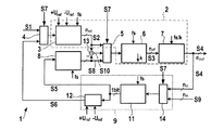
ΔΣデータ変換装置1は、図1によれば、破線で区画されたΔΣアナログデジタル変換器(ΔΣADC)2を有している。ΔΣアナログデジタル変換器2は、例えばセンサの測定信号などのアナログ入力信号81を受け取り、それ自体公知の仕方でデジタル出力信号S4を出力する。このデジタル出力信号S4は例えば下位の制御装置または評価装置によって受け取られる。このために、ΔΣADC2は、通常動作には関係のない、スイッチとして機能する入力マルチプレクサ4を介してアナログ入力信号S1を受け取るアナログデルタシグマ変調器(ΔΣ変調器)3を有している。
According to FIG. 1, the
アナログΔΣ変調器3はその入力段において、それ自体公知の仕方で、高サンプリング周波数fsでのサンプリングによりアナログ入力信号S1の時間離散化を行う。その際、ΔΣ変調器3は基準電圧+Urefおよび−Urefに接続されており、それゆえアナログ電圧信号S1は、Urefによって定まる電圧領域内で、狭いワード幅nsdと帯域幅fs/2をもったパルス密度変調されたデジタルデータストリーム信号S2を出力する。アナログΔΣ変調器3は、例えば、アナログ電圧値を積分ないし積算するための積分器と、例えばコンパレータによって形成される量子化器と、場合によっては、印加されるクロック信号fsに応じてデータストリーム信号S2を出力する出力メモリとを具えた従来の構造を有しており、この構造において、デジタルアナログ変換器を介してアナログ加算器へ出力信号ないしデジタルデータストリーム信号S2の負のフィードバックが行われる、または、検出すべきアナログ入力信号S1とこのアナログフィードバック信号との差が求められる。したがって、データストリームS2は、アナログ入力信号S1に応じて、パルス密度変調された信号として形成される。アナログΔΣ変調器3は有利にはワード幅nsd=1ビットで構成しうる。そのため、信号S2はパルス密度変調されたビットストリームを形成することとなり、これにより高い線形性がもたらされる。クロック信号fsは例えば2〜3MHzの範囲とすることができ、後に出力されるデジタル出力信号S4に比べて、1に対して例えば1000という範囲の、非常に高い明らかなオーバーサンプリングを提供する。 In the input stage, the analog ΔΣ modulator 3 performs time discretization of the analog input signal S1 by sampling at a high sampling frequency fs in a manner known per se. In this case, the ΔΣ modulator 3 is connected to the reference voltages + U ref and −U ref , and therefore the analog voltage signal S1 is narrow in the voltage region determined by U ref and has a narrow word width n sd and a bandwidth fs / 2. And a digital data stream signal S2 modulated with pulse density. The analog ΔΣ modulator 3 includes, for example, an integrator for integrating or integrating analog voltage values, a quantizer formed by, for example, a comparator, and, in some cases, a data stream signal according to an applied clock signal fs. And having a conventional structure including an output memory for outputting S2, in which a negative feedback of the output signal or the digital data stream signal S2 is performed to the analog adder via the digital-analog converter. Alternatively, the difference between the analog input signal S1 to be detected and the analog feedback signal is obtained. Thus, the data stream S2 is formed as a pulse density modulated signal in response to the analog input signal S1. The analog ΔΣ modulator 3 can advantageously be configured with a word width n sd = 1 bit. The signal S2 thus forms a pulse density modulated bit stream, which results in a high linearity. The clock signal fs can be in the range of 2 to 3 MHz, for example, and provides a very high apparent oversampling, for example in the range of 1000 to 1 compared to the digital output signal S4 output later.
デジタルデータストリームS2はスイッチとして機能するマルチプレクサ5を介してデジタルデシメーションフィルタ6に供給される。デジタルデシメーションフィルタ6はフィルタリングと間引き率kでのダウンサンプリングとを行い、ndf>>nsdのワード幅ndfと帯域幅fs/2kをもつ出力信号S3を供給する。信号路上で後置されたデジタルローパスフィルタ7はこの信号S3を受け取り、それに含まれている雑音成分の抑制と有効帯域における伝達特性の補償とに使用される。デジタルローパスフィルタ7はワード幅noutのデジタル出力信号S4を出力する。
The digital data stream S2 is supplied to a
本発明によれば、ΔΣADC2を検査する検査装置がさらに設けられており、この検査装置はデジタル基準装置として機能するデジタルΔΣ基準変調器8とテスト信号発生器9を有している。ここで、既に述べたマルチプレクサ4および5とテスト信号発生器9内に設けられたマルチプレクサ10はスイッチとして機能する。
According to the present invention, an inspection device for inspecting the
テスト信号発生器9は有利には低次の、例えば1次の、デジタルΔΣ変調器11を有しており、デジタルΔΣ変調器11はその入力信号から1ビットのワード幅とfs/2の帯域幅をもつデジタルテスト信号S5を生成する。デジタルテスト信号S5はデジタルΔΣ基準変調器8に直接入力され、さらに1ビットD/A変換器12を介してアナログテスト信号S6に変換される。その際、例えばデジタル値域(+1,−1)は相応するアナログ値域(+Uref,−Uref)に写像される。ここで、Urefは有利にはアナログΔΣ変調器3の基準電圧に相当する。アナログテスト信号S6はマルチプレクサ4に出力される。マルチプレクサ4は制御信号S7によって駆動され、制御信号S7に応じて選択的にアナログ入力信号S1またはアナログテスト信号S6をアナログΔΣ変調器3に出力する。
The
図3には、アナログ入力信号S1とアナログ値で記述される基準電圧+Urefおよび−Urefのための3つの入力側を有する共通のスイッチによってDAC12と入力マルチプレクサ4を組み合わせた回路技術的に単純な構造が示されている。ここで、2進値[0,1]を[−Uref,+Uref]に写像するため、S7=,,0''のときにはスイッチK2,K3が開き、スイッチK1は閉じ、S7=,,1''のときにはスイッチK1が開き、K2またはK3はS5に応じて交互に閉じる。したがって、K2のスイッチ位置はS5により制御され、相応してK3のスイッチ位置は反転値NOT(S5)により制御される。これに相応して、アナログ信号S6は+Urefまたは−Urefの接続によって直接形成される。
FIG. 3 shows a circuit technically simple combination of the
デジタル基準変調器8はアナログΔΣ変調器3の伝達関数(Z変換)を正確なデジタル計算アルゴリズムの形で理想的にモデル化する。デジタル基準変調器8はデジタル入力信号S5からワード幅nsdと帯域幅fs/2とをもつパルス密度変調されたデジタル基準データストリーム信号S8を形成する。ここで、デジタルΔΣ基準変調器8は有利にはハードウェア的に形成されているが、デジタル計算アルゴリズムは原則的に例えばソフトウェア的にも実行することができる。
The
デジタル加算器13はアナログΔΣ変調器3とデジタル基準変調器8の出力信号の差信号S10=S2−S8を形成する。この信号のワード幅nsdは有利には1ビットと小さいので、これに相応してデジタル加算器13のための回路技術上のコストも同様に低い。
The
テスト信号発生器9のデジタルΔΣ変調器11にはまた別のマルチプレクサ14が前置接続されており、このマルチプレクサ14はデジタル出力信号S4とさらにテストデータ入力信号S9を受け取り、制御信号S7に応じてこれらの信号S4,S9のうちの一方を通す。ここで、テストデータ入力信号S9はデジタル出力信号S4のワード幅に相当するワード幅ninを有している。
Another
テスト信号S5は変調されたテストデータ信号S9またはフィードバックされた出力信号S4とΔΣ変調器11の量子化雑音の成分とから構成されている。テストデータ入力信号S9のワード幅は、図2に従って、全入力範囲にわたる量子化雑音のレベルがテストデータ入力信号S9のLSB(最下位ビット)に関してステップ幅ΔMよりも大きくなるように選ばれる。このようにしてテスト信号S5は生成される。テスト信号S5は、一方では、図2の横軸に示された少数の、有利には2exp(nin−1)の、データ点を有する特性曲線全体をカバーする本来の有効帯域におけるワード幅が小さいという理由から、他方では、同様にテスト信号S5の構成成分として有効な広帯域雑音が重畳されているという理由から、検査すべきΔΣADC2の全値域を刺激する。
The test signal S5 includes a modulated test data signal S9 or a feedback output signal S4 and a quantization noise component of the
制御信号S7を用いれば、アナログ入力信号S1を受け取ってデジタル出力信号S4を出力する通常動作モードの他に、それぞれBIST(組込自己テスト)テストモードを表す少なくとも3つのテストモードを選択することができる。 Using the control signal S7, in addition to the normal operation mode in which the analog input signal S1 is received and the digital output signal S4 is output, at least three test modes each representing a BIST (Built-in Self Test) test mode can be selected. it can.
第1および第2のテストモードでは、装置のデジタルコンポーネントがテストされる。アナログΔΣ変調器3の出力側はこの動作モードでは使用されない。 In the first and second test modes, the digital components of the device are tested. The output side of the analog ΔΣ modulator 3 is not used in this operation mode.
第1のテストモードは基本的な機能検査に使用される。マルチプレクサ14を介してデジタルテストデータ信号S9はテスト信号発生器9の入力側に印加される。テスト信号発生器9はこのデジタルテストデータ信号S9からデジタルテスト信号S5を形成し、基準変調器8に出力する。基準変調器8によって出力された基準データストリーム信号S8はマルチプレクサ5を経てデシメーションフィルタ6の入力側に達し、そこからローパスフィルタ7を経て出力信号S4として出力される。それゆえ、この動作モードにおいては出力信号S4が入力データの像であり、直接比較によって機能的に検査される。
The first test mode is used for basic functional testing. The digital test data signal
第2のテストモードは、第1のテストモードの変形として、テスト信号発生器9のテストデータ入力側への出力信号S4のフィードバックにより行われる。S4の有利には下位ninビットの負のフィードバックにより、上で述べた信号路全体を短期間のあいだ全値域にわたって刺激する広帯域の疑似ランダムテスト信号S5が生じる。
The second test mode is performed by feedback of the output signal S4 to the test data input side of the
この動作モードにおいて全信号路は同期したデジタルネットワークとして機能するので、本来のテストは、出力データS4が相応するシミュレーション結果と同一であるかを「テストパターン」に基づいて繰り返し検査することにより行うことができる。「テストパターン」の誤差シミュレーションにより、所定のテストマスクに達するのに最適な検査持続時間が定められる。このようにして、スキャンパスを用いた構造的テストに代わって、デジタル装置の意図された機能を自動的に生成される刺激によって固定マスクを監視することで検査することができる。 Since all signal paths function as a synchronized digital network in this operation mode, the original test is performed by repeatedly checking whether the output data S4 is the same as the corresponding simulation result based on the “test pattern”. Can do. The error duration of the “test pattern” determines the optimum inspection duration for reaching a predetermined test mask. In this way, instead of a structural test using the scan path, the intended function of the digital device can be examined by monitoring the fixed mask with a stimulus that is automatically generated.
第3のテストモードでは、同じ刺激の下でアナログΔΣ変調器3の出力データストリームをデジタル基準変調器8の出力データストリームと比較することにより、アナログΔΣ変調器3が検証される。
In the third test mode, the analog ΔΣ modulator 3 is verified by comparing the output data stream of the analog ΔΣ modulator 3 with the output data stream of the
テストデータ入力信号S9はマルチプレクサ4を経てデジタルΔΣ変調器11に達し、デジタルΔΣ変調器11の出力側にワード幅1ビット、帯域幅fs/2のパルス密度変調されたテスト信号S5として現れる。値域(+1,−1)のデジタルテスト信号S5はふたたび基準変調器8に入力されるのと同時に、相応する値域(+Uref,−Uref)のアナログ形式S6で、検査すべきアナログΔΣ変調器3の入力信号として使用される。デジタル加算器13は差信号S10=S2−S8を形成し、差信号S10はマルチプレクサ13を介して後続のフィルタ段6および7に転送される。変調器3および8の量子化雑音の高周波雑音成分はフィルタ段で除去され、信号帯域幅はfs/2kに低減される。それゆえ、残余信号S4はS10の有効信号帯域の差を表す。両方の変調器が同じ入力信号で刺激されるので、S4における結果はΔΣ変調器3の理想的な基準モデル8からの偏差であり、S9によって決まる動作点においてのそのつどの誤差を表す。S9の値域を例えばデジタルカウンタが直線的に走破することにより、出力側S4では2**nin個のデータ点をもつΔΣADCの誤差曲線が得られる。
The test data input signal S9 reaches the
図4には、フローチャートの一例が示されている。このフローチャートにおいて、テストモードBIST1,2,3はI,II,IIIで表されており、連続して実行される。このために、制御装置を介して外部から制御信号S7がマルチプレクサ4,5,14に入力され、テストデータ入力信号S9がマルチプレクサ14に入力される。
FIG. 4 shows an example of a flowchart. In this flowchart, test modes BIST1, 2, 3 are represented by I, II, III and are executed continuously. For this purpose, the control signal S7 is input to the
ステップSt1におけるスタートの後、まずステップSt2に従ってテストモードBIST1においてテストデータ入力信号S9がテスト信号発生器9に入力され、ステップSt3においてテスト信号発生器9によりデジタルテスト信号S5が生成および出力され、その後、ステップSt4において、デジタルΔΣ基準変調器8によりデジタルテスト信号S5からデジタル基準データストリーム信号S8が生成される。デジタル基準データストリーム信号S8はステップSt5においてデジタルフィルタ装置6,7によりフィルタリングされ、その後、ステップSt6において評価される。
After the start in step St1, first, the test data input signal S9 is input to the
テストモードBIST2では、ステップSt7においてデジタル出力信号S4がテスト信号発生器9に供給され、ステップSt8においてテスト信号発生器9によりデジタルテスト信号S5が出力され、デジタルΔΣ基準変調器8に供給され、ステップSt9においてデジタルΔΣ基準変調器8により基準データストリーム信号S8が形成される。この基準データストリーム信号S8はその後ステップSt10においてフィルタリングされ、ステップSt11において評価される。
In the test mode BIST2, the digital output signal S4 is supplied to the
続いて、テストモードBIST3が実行される。テストモードBIST3によれば、ステップSt12において信号S9が入力され、ステップSt13においてまず再度デジタルテスト信号S5が形成され、続いてステップSt14においてデジタルアナログ変換器12によりこのデジタルテスト信号S5からアナログテスト信号S6が形成され、マルチプレクサ4を介してアナログΔΣ変調器3に供給される。続いて、ステップSt15において差信号S10が形成され、ステップSt16におけるフィルタリングの後、ステップSt17において評価される。その際、BIST3では補足的に信号S2およびS8も個々にフィルタリングし、評価してよい。
Subsequently, the test mode BIST3 is executed. According to the test mode BIST3, the signal S9 is input in step St12, the digital test signal S5 is first formed again in step St13, and then the digital test signal S5 is converted from the digital test signal S5 by the digital /
このように、自己テストプロセスないし検査プロセスはステップSt17で終了するので、続くステップSt18においてアナログ入力信号S1の受信および評価によって測定を開始することができる。 Thus, since the self-test process or the inspection process ends in step St17, the measurement can be started by receiving and evaluating the analog input signal S1 in the subsequent step St18.
1 ΔΣデータ変換装置
2 ΔΣアナログデジタル変換器
3 アナログΔΣ変調器
4 マルチプレクサ
5 マルチプレクサ
6 デジタルデシメーションフィルタ
7 デジタルローパスフィルタ
8 ΔΣ基準変調器
9 テスト信号発生器
10 マルチプレクサ
11 デジタルΔΣ変調器
12 デジタルアナログ変換器
13 デジタル加算器
14 マルチプレク
1
Claims (19)
アナログ入力信号(S1)を受け取って、デジタルデータストリーム信号(S2)を出力するアナログΔΣ変調器(3)と、
少なくとも前記デジタルデータストリーム信号(S2)を受け取って、デジタル出力信号(S4)を出力するデジタルフィルタ装置(6,7)と、
前記デジタルデータストリーム信号(S2)から導出された信号(S4)に応じてテスト信号(S5,S6)を生成するテスト信号発生器(9,11,12,14)と、
前記テスト信号(S5)を受け取って、デジタル基準データストリーム信号(S8)を出力するデジタル基準装置(8)と、
前記デジタルデータストリーム信号(S2)と前記デジタル基準データストリーム信号(S8)を受け取って、少なくとも前記デジタルデータストリーム信号(S2)と前記デジタル基準データストリーム信号(S8)を前記デジタルフィルタ装置(6,7)に出力する信号受け取り装置(13,5)を有していることを特徴とする、ΔΣデータ変換装置。 In the ΔΣ data converter, at least,
An analog ΔΣ modulator (3) that receives an analog input signal (S1) and outputs a digital data stream signal (S2);
A digital filter device (6, 7) for receiving at least the digital data stream signal (S2) and outputting a digital output signal (S4);
A test signal generator (9, 11, 12, 14) for generating test signals (S5, S6) in response to a signal (S4) derived from the digital data stream signal (S2);
A digital reference device (8) that receives the test signal (S5) and outputs a digital reference data stream signal (S8);
The digital data stream signal (S2) and the digital reference data stream signal (S8) are received, and at least the digital data stream signal (S2) and the digital reference data stream signal (S8) are received by the digital filter device (6, 7). A ΔΣ data conversion device, characterized in that it has a signal receiving device (13, 5) that outputs to (1).
Applications Claiming Priority (2)
| Application Number | Priority Date | Filing Date | Title |
|---|---|---|---|
| DE200610050175 DE102006050175A1 (en) | 2006-10-25 | 2006-10-25 | A delta-sigma data converter arrangement and method for verifying a delta-sigma data converter |
| DE102006050175.6 | 2006-10-25 |
Publications (3)
| Publication Number | Publication Date |
|---|---|
| JP2008109671A JP2008109671A (en) | 2008-05-08 |
| JP2008109671A5 JP2008109671A5 (en) | 2010-12-09 |
| JP4940101B2 true JP4940101B2 (en) | 2012-05-30 |
Family
ID=38920745
Family Applications (1)
| Application Number | Title | Priority Date | Filing Date |
|---|---|---|---|
| JP2007277385A Active JP4940101B2 (en) | 2006-10-25 | 2007-10-25 | ΔΣ data converter and inspection method for ΔΣ data converter |
Country Status (4)
| Country | Link |
|---|---|
| EP (1) | EP1916771B1 (en) |
| JP (1) | JP4940101B2 (en) |
| DE (2) | DE102006050175A1 (en) |
| TW (1) | TWI431945B (en) |
Families Citing this family (5)
| Publication number | Priority date | Publication date | Assignee | Title |
|---|---|---|---|---|
| DE102010032296B4 (en) * | 2009-08-26 | 2014-05-28 | Sew-Eurodrive Gmbh & Co Kg | Method for processing a measured value signal representing an analogue value for output current of an inverter and apparatus for carrying out the method |
| CN104459521B (en) * | 2014-12-19 | 2017-03-01 | 中国科学院微电子研究所 | System of selection based on bit stream in △ ∑ analog stimulus generation method in the piece of memorizer |
| US9768793B2 (en) * | 2015-12-17 | 2017-09-19 | Analog Devices Global | Adaptive digital quantization noise cancellation filters for mash ADCs |
| US10653904B2 (en) | 2017-12-02 | 2020-05-19 | M-Fire Holdings, Llc | Methods of suppressing wild fires raging across regions of land in the direction of prevailing winds by forming anti-fire (AF) chemical fire-breaking systems using environmentally clean anti-fire (AF) liquid spray applied using GPS-tracking techniques |
| US11901919B2 (en) | 2021-04-26 | 2024-02-13 | Stmicroelectronics International N.V. | On chip test architecture for continuous time delta sigma analog-to-digital converter |
Family Cites Families (3)
| Publication number | Priority date | Publication date | Assignee | Title |
|---|---|---|---|---|
| US5068657A (en) * | 1990-05-25 | 1991-11-26 | At&T Bell Laboratories | Method and apparatus for testing delta-sigma modulators |
| US5257026A (en) * | 1992-04-17 | 1993-10-26 | Crystal Semiconductor, Inc. | Method and apparatus for calibrating a multi-bit delta-sigma modular |
| US5959562A (en) * | 1997-09-03 | 1999-09-28 | Analog Devices, Inc. | Sigma-delta modulator and method for operating such modulator |
-
2006
- 2006-10-25 DE DE200610050175 patent/DE102006050175A1/en not_active Withdrawn
-
2007
- 2007-09-03 EP EP20070115504 patent/EP1916771B1/en active Active
- 2007-09-03 DE DE200750002389 patent/DE502007002389D1/en active Active
- 2007-10-23 TW TW96139638A patent/TWI431945B/en active
- 2007-10-25 JP JP2007277385A patent/JP4940101B2/en active Active
Also Published As
| Publication number | Publication date |
|---|---|
| EP1916771B1 (en) | 2009-12-23 |
| JP2008109671A (en) | 2008-05-08 |
| DE102006050175A1 (en) | 2008-04-30 |
| DE502007002389D1 (en) | 2010-02-04 |
| TWI431945B (en) | 2014-03-21 |
| TW200832926A (en) | 2008-08-01 |
| EP1916771A1 (en) | 2008-04-30 |
Similar Documents
| Publication | Publication Date | Title |
|---|---|---|
| EP3242404B1 (en) | Delta sigma patterns for calibrating a digital-to-analog converter | |
| US8830098B2 (en) | Sigma-delta ADC with test circuitry | |
| JP4940101B2 (en) | ΔΣ data converter and inspection method for ΔΣ data converter | |
| TW200810371A (en) | Asynchronous sigma-delta digital-analog converter | |
| US6111529A (en) | Accurate gain calibration of analog to digital converters | |
| EP3182594B1 (en) | Frequency-domain adc flash calibration | |
| Barragan et al. | A fully-digital BIST wrapper based on ternary test stimuli for the dynamic test of a 40 nm CMOS 18-bit stereo audio $\Sigma\Delta $ ADC | |
| TWI233495B (en) | IC with built-in self-test function and design method thereof | |
| Bhatheja et al. | Low cost high accuracy stimulus generator for on-chip spectral testing | |
| Hung et al. | A Fully Integrated BIST $\Delta\Sigma $ ADC Using the In-Phase and Quadrature Waves Fitting Procedure | |
| Jiang et al. | Built-in Self-Calibration of On-chip DAC and ADC | |
| Hong et al. | A Fully Integrated Built-In Self-Test $\Sigma {-}\Delta $ ADC Based on the Modified Controlled Sine-Wave Fitting Procedure | |
| Rolindez et al. | A stereo audio Σ∑ ADC architecture with embedded SNDR self-test | |
| WO2007009912A1 (en) | Method for testing analog-to-digital converters | |
| Sahu et al. | System level behavioral modeling of CORDIC based ORA of built-in-self-test for sigma-delta analog-to-digital converter | |
| Sahu et al. | A review on system level behavioral modeling and post simulation of built-in-self-test of sigma-delta modulator analog-to-digital converter | |
| Zhao et al. | An active CMOS NMR field probe with custom transceiver and ΣΔ modulator ASICs and an optical link | |
| Vázquez et al. | Practical solutions for the application of the oscillation-based-test in analog integrated circuits | |
| Sahu et al. | Optimized System Level Hardware Realization of Built-in-Self-Test Approach for Sigma-Delta Analog-to-Digital Converter | |
| Ankur et al. | A novel on-chip mismatch measurement technique for Nyquist rate ADCs | |
| Hong | Design-for-digital-testability 30 MHz second-order/spl Sigma/-/spl Delta/modulator | |
| Kim et al. | Capacitor-coupled built-off self-test in analog and mixed-signal embedded systems | |
| Andrejević et al. | Fault effects in sigma-delta modulator | |
| Kook et al. | Signature Testing and Diagnosis of High Precision S? ADC Dynamic Specifications Using Model Parameter Estimation | |
| Sahu et al. | High level computation technique for characterization of sigma-delta a/d converter |
Legal Events
| Date | Code | Title | Description |
|---|---|---|---|
| A521 | Request for written amendment filed |
Free format text: JAPANESE INTERMEDIATE CODE: A523 Effective date: 20101025 |
|
| A621 | Written request for application examination |
Free format text: JAPANESE INTERMEDIATE CODE: A621 Effective date: 20101025 |
|
| RD04 | Notification of resignation of power of attorney |
Free format text: JAPANESE INTERMEDIATE CODE: A7424 Effective date: 20101227 |
|
| A977 | Report on retrieval |
Free format text: JAPANESE INTERMEDIATE CODE: A971007 Effective date: 20110930 |
|
| A131 | Notification of reasons for refusal |
Free format text: JAPANESE INTERMEDIATE CODE: A131 Effective date: 20111013 |
|
| A521 | Request for written amendment filed |
Free format text: JAPANESE INTERMEDIATE CODE: A523 Effective date: 20120111 |
|
| TRDD | Decision of grant or rejection written | ||
| A01 | Written decision to grant a patent or to grant a registration (utility model) |
Free format text: JAPANESE INTERMEDIATE CODE: A01 Effective date: 20120127 |
|
| A01 | Written decision to grant a patent or to grant a registration (utility model) |
Free format text: JAPANESE INTERMEDIATE CODE: A01 |
|
| A61 | First payment of annual fees (during grant procedure) |
Free format text: JAPANESE INTERMEDIATE CODE: A61 Effective date: 20120227 |
|
| FPAY | Renewal fee payment (event date is renewal date of database) |
Free format text: PAYMENT UNTIL: 20150302 Year of fee payment: 3 |
|
| R150 | Certificate of patent or registration of utility model |
Ref document number: 4940101 Country of ref document: JP Free format text: JAPANESE INTERMEDIATE CODE: R150 Free format text: JAPANESE INTERMEDIATE CODE: R150 |
|
| R250 | Receipt of annual fees |
Free format text: JAPANESE INTERMEDIATE CODE: R250 |
|
| R250 | Receipt of annual fees |
Free format text: JAPANESE INTERMEDIATE CODE: R250 |
|
| R250 | Receipt of annual fees |
Free format text: JAPANESE INTERMEDIATE CODE: R250 |
|
| R250 | Receipt of annual fees |
Free format text: JAPANESE INTERMEDIATE CODE: R250 |
|
| R250 | Receipt of annual fees |
Free format text: JAPANESE INTERMEDIATE CODE: R250 |
|
| R250 | Receipt of annual fees |
Free format text: JAPANESE INTERMEDIATE CODE: R250 |
|
| R250 | Receipt of annual fees |
Free format text: JAPANESE INTERMEDIATE CODE: R250 |
|
| R250 | Receipt of annual fees |
Free format text: JAPANESE INTERMEDIATE CODE: R250 |
|
| R250 | Receipt of annual fees |
Free format text: JAPANESE INTERMEDIATE CODE: R250 |
|
| R250 | Receipt of annual fees |
Free format text: JAPANESE INTERMEDIATE CODE: R250 |