JP4871378B2 - Semiconductor light emitting element array apparatus, image exposure apparatus, image forming apparatus, and image display apparatus - Google Patents
Semiconductor light emitting element array apparatus, image exposure apparatus, image forming apparatus, and image display apparatus Download PDFInfo
- Publication number
- JP4871378B2 JP4871378B2 JP2009193065A JP2009193065A JP4871378B2 JP 4871378 B2 JP4871378 B2 JP 4871378B2 JP 2009193065 A JP2009193065 A JP 2009193065A JP 2009193065 A JP2009193065 A JP 2009193065A JP 4871378 B2 JP4871378 B2 JP 4871378B2
- Authority
- JP
- Japan
- Prior art keywords
- emitting element
- semiconductor light
- light emitting
- substrate
- thin film
- Prior art date
- Legal status (The legal status is an assumption and is not a legal conclusion. Google has not performed a legal analysis and makes no representation as to the accuracy of the status listed.)
- Active
Links
Images


Classifications
-
- H—ELECTRICITY
- H01—ELECTRIC ELEMENTS
- H01L—SEMICONDUCTOR DEVICES NOT COVERED BY CLASS H10
- H01L25/00—Assemblies consisting of a plurality of individual semiconductor or other solid state devices ; Multistep manufacturing processes thereof
- H01L25/03—Assemblies consisting of a plurality of individual semiconductor or other solid state devices ; Multistep manufacturing processes thereof all the devices being of a type provided for in the same subgroup of groups H01L27/00 - H01L33/00, or in a single subclass of H10K, H10N, e.g. assemblies of rectifier diodes
- H01L25/04—Assemblies consisting of a plurality of individual semiconductor or other solid state devices ; Multistep manufacturing processes thereof all the devices being of a type provided for in the same subgroup of groups H01L27/00 - H01L33/00, or in a single subclass of H10K, H10N, e.g. assemblies of rectifier diodes the devices not having separate containers
- H01L25/075—Assemblies consisting of a plurality of individual semiconductor or other solid state devices ; Multistep manufacturing processes thereof all the devices being of a type provided for in the same subgroup of groups H01L27/00 - H01L33/00, or in a single subclass of H10K, H10N, e.g. assemblies of rectifier diodes the devices not having separate containers the devices being of a type provided for in group H01L33/00
- H01L25/0753—Assemblies consisting of a plurality of individual semiconductor or other solid state devices ; Multistep manufacturing processes thereof all the devices being of a type provided for in the same subgroup of groups H01L27/00 - H01L33/00, or in a single subclass of H10K, H10N, e.g. assemblies of rectifier diodes the devices not having separate containers the devices being of a type provided for in group H01L33/00 the devices being arranged next to each other
-
- H—ELECTRICITY
- H01—ELECTRIC ELEMENTS
- H01L—SEMICONDUCTOR DEVICES NOT COVERED BY CLASS H10
- H01L2924/00—Indexing scheme for arrangements or methods for connecting or disconnecting semiconductor or solid-state bodies as covered by H01L24/00
- H01L2924/0001—Technical content checked by a classifier
- H01L2924/0002—Not covered by any one of groups H01L24/00, H01L24/00 and H01L2224/00
Description
本発明は、規則的に配列された複数の半導体発光素子を有する半導体発光素子アレイ装置、この半導体発光素子アレイ装置を備えた画像露光装置、この画像露光装置を備えた電子写真式の画像形成装置、及び前記半導体発光素子アレイ装置を備えた画像表示装置に関するものである。 The present invention relates to a semiconductor light emitting element array apparatus having a plurality of regularly arranged semiconductor light emitting elements, an image exposure apparatus including the semiconductor light emitting element array apparatus, and an electrophotographic image forming apparatus including the image exposure apparatus. And an image display device including the semiconductor light emitting element array device.
一般に、半導体発光素子を異種材料基板上に集積する際には、ダイシング又は劈開によってチップ化された半導体発光素子チップ(例えば、250〜300μm厚)をダイボンディングペースト又は接着剤などを用いて異種材料基板上に固定し、半導体発光素子チップの接続パッドと異種材料基板上の電気配線とをAuボンディングワイヤを用いて接続している。また、異種材料基板上に半導体発光素子チップ及び駆動回路チップを接着し、両チップ間をAuボンディングワイヤを用いて接続する技術も知られている。しかし、これらの方法では、ダイシング又は劈開によって半導体発光素子チップを製造しているので、チップサイズの十分なシュリンクが困難であった。また、半導体発光素子チップ及び駆動回路チップには、Auボンディングワイヤを結線するための接続パッド(例えば、50μm×50μm以上)を備える必要があり、この点からもチップサイズの十分なシュリンクは困難であった。 In general, when a semiconductor light emitting device is integrated on a dissimilar material substrate, a semiconductor light emitting device chip (for example, 250 to 300 μm thick) formed into chips by dicing or cleaving is used by using a die bonding paste or an adhesive. It is fixed on the substrate, and the connection pads of the semiconductor light emitting element chip and the electrical wiring on the dissimilar material substrate are connected using Au bonding wires. There is also known a technique in which a semiconductor light emitting element chip and a driving circuit chip are bonded on a different material substrate and the two chips are connected using an Au bonding wire. However, in these methods, since the semiconductor light emitting element chip is manufactured by dicing or cleaving, it is difficult to sufficiently shrink the chip size. In addition, the semiconductor light emitting element chip and the drive circuit chip need to be provided with connection pads (for example, 50 μm × 50 μm or more) for connecting Au bonding wires. From this point, it is difficult to shrink the chip sufficiently. there were.
そこで、半導体発光素子を含む半導体発光素子薄膜であるLEDエピタキシャルフィルム(例えば、5μm厚以下)を基板上に密着固定し、半導体発光素子薄膜の電極層と基板上の電気配線とを、ホトリソグラフィ技術と蒸着法又はスパッタ法を組み合わせることにより形成可能な配線層によって接続する技術の提案がある(例えば、特許文献1参照)。この技術によれば、ダイシング及び劈開を用いずに半導体発光素子薄膜を形成でき、且つ、ボンディングワイヤ接続用の接続パッドが不要になるので、半導体発光素子薄膜のサイズの十分なシュリンクが可能である。 Therefore, an LED epitaxial film (for example, 5 μm or less), which is a semiconductor light-emitting element thin film including a semiconductor light-emitting element, is adhered and fixed on the substrate, and the electrode layer of the semiconductor light-emitting element thin film and the electric wiring on the substrate are photolithography technology. There is a proposal of a technique of connecting by a wiring layer that can be formed by combining a vapor deposition method or a sputtering method (see, for example, Patent Document 1). According to this technique, a semiconductor light emitting element thin film can be formed without using dicing and cleavage, and a connection pad for bonding wire connection is not required, and thus the size of the semiconductor light emitting element thin film can be sufficiently reduced. .
しかしながら、特許文献1に記載の装置では、基板上に密着固定された複数の半導体発光素子薄膜の内の一部(例えば、1個)に不具合(例えば、位置ずれ又は外観異常など)が発見された場合であっても、不具合箇所のみを修理することが難しく、通常は、装置全体を廃棄する必要があった。 However, in the apparatus described in Patent Document 1, a defect (for example, misalignment or abnormal appearance) is found in a part (for example, one) of a plurality of semiconductor light emitting element thin films that are closely fixed on the substrate. Even in this case, it is difficult to repair only the defective part, and it is usually necessary to discard the entire apparatus.
この理由は、基板上に密着固定される半導体発光素子薄膜の材料として、選択的にケミカルエッチングが困難な材料、例えば、(AlxGa1−x)yIn1−yP、GaP、GaN、AlxGa1−xN、InxGa1−xNなどを用い、この半導体発光素子薄膜を、SiO2又はSiNなどの無機材料から成る接合面上、Au又はPdなどのメタル材料から成る接合面上、又は、ポリイミド、アクリル、SOG、ノボラックなどの有機材料から成る接合面上に接着した場合には、接合面に損傷を与えずに半導体発光素子薄膜を基板からの除去することが困難になるからである。 This is because, as a material of the semiconductor light-emitting element thin film that is tightly fixed on the substrate, a material that is selectively difficult to chemically etch, for example, (Al x Ga 1-x ) y In 1-y P, GaP, GaN, Using Al x Ga 1-x N, In x Ga 1-x N, etc., this semiconductor light-emitting element thin film is bonded on a bonding surface made of an inorganic material such as SiO 2 or SiN, and made of a metal material such as Au or Pd. When bonded on a surface or a bonding surface made of an organic material such as polyimide, acrylic, SOG, or novolac, it is difficult to remove the semiconductor light-emitting element thin film from the substrate without damaging the bonding surface. Because it becomes.
また、他の理由は、たとえ半導体発光素子薄膜の材料として、選択的にケミカルエッチングが可能な材料、例えば、AlxGa1−xAs、GaAsなどを用いたとしても、ケミカルエッチングで半導体発光素子薄膜を除去した後の基板表面は、除去工程によって荒らされて粗面になっており、再度、その上に半導体発光素子薄膜を密着固定させることが困難だからである。 Another reason is that even if a material that can be selectively subjected to chemical etching, for example, Al x Ga 1-x As, GaAs, or the like, is used as a material for the semiconductor light emitting element thin film, the semiconductor light emitting element can be formed by chemical etching. This is because the substrate surface after removing the thin film is roughened by the removing process to become a rough surface, and it is difficult to fix the semiconductor light emitting element thin film on the surface again.
そこで、本発明は、上記従来技術の課題を解決するためになされたものであり、その目的は、規則的に配列された複数の半導体発光素子の内の一部の半導体発光素子のみを交換可能にした半導体発光素子アレイ装置、この半導体発光素子アレイ装置を備えた画像露光装置、画像形成装置、及び画像表示装置を提供することである。 Accordingly, the present invention has been made to solve the above-described problems of the prior art, and its purpose is to replace only a part of the plurality of regularly arranged semiconductor light emitting elements. And providing an image exposure apparatus, an image forming apparatus, and an image display apparatus including the semiconductor light emitting element array apparatus.
本発明に係る半導体発光素子アレイ装置は、基板と、前記基板上に備えられた複数のリムーバブル層と、前記複数のリムーバブル層上に備えられ、前記基板の表面材料とは異なる材料から構成され、半導体発光素子を備える半導体発光素子薄膜とを有し、前記複数のリムーバブル層は、ケミカルエッチングによって選択的にエッチング可能な材料で構成されていることを特徴としている。 A semiconductor light-emitting element array device according to the present invention comprises a substrate, a plurality of removable layers provided on the substrate, and a material different from a surface material of the substrate, provided on the plurality of removable layers, A plurality of removable layers, wherein the plurality of removable layers are made of a material that can be selectively etched by chemical etching.
また、本発明に係る画像露光装置は、半導体発光素子アレイを含む画像露光部を有する画像露光装置であって、前記発光素子アレイは、基板と、前記基板上に備えられた複数のリムーバブル層と、前記複数のリムーバブル層上に備えられ、前記基板の表面材料とは異なる材料から構成され、半導体発光素子を備える半導体発光素子薄膜とを有し、前記複数のリムーバブル層は、ケミカルエッチングによって前記基板に対して選択的にエッチング可能な材料で構成され、前記複数のリムーバブル層のそれぞれの上には、前記半導体発光素子薄膜が1つ設けられることを特徴としている。
また、本発明に係る別の画像露光装置は、半導体発光素子アレイを含む画像露光部を有する画像露光装置であって、前記発光素子アレイは、基板と、前記基板上に備えられた複数のリムーバブル層と、前記リムーバブル層上に備えられた裏面電極層と、前記裏面電極層上に備えられ、前記基板の表面材料とは異なる材料から構成され、半導体発光素子を備える半導体発光素子薄膜とを有し、前記複数のリムーバブル層は、ケミカルエッチングによって選択的にエッチング可能な材料で構成され、前記半導体発光素子薄膜は、前記裏面電極層上に分子間力、水素結合、陽極接合、接着剤のいずれかにより固定されていることを特徴としている。
The image exposure apparatus according to the present invention is an image exposure apparatus having an image exposure unit including a semiconductor light emitting element array, wherein the light emitting element array includes a substrate and a plurality of removable layers provided on the substrate. A semiconductor light-emitting element thin film including a semiconductor light-emitting element that is provided on the plurality of removable layers and is made of a material different from a surface material of the substrate, and the plurality of removable layers are formed by chemical etching on the substrate. selectively consists of etchable material to, on each of said plurality of removable layers, the semiconductor light emitting element thin film is one provided wherein Rukoto.
Another image exposure apparatus according to the present invention is an image exposure apparatus having an image exposure unit including a semiconductor light emitting element array, the light emitting element array comprising a substrate and a plurality of removable devices provided on the substrate. A layer, a back electrode layer provided on the removable layer, and a semiconductor light emitting device thin film provided on the back electrode layer, made of a material different from the surface material of the substrate, and comprising a semiconductor light emitting device. The plurality of removable layers are made of a material that can be selectively etched by chemical etching, and the semiconductor light-emitting element thin film is formed of any of intermolecular force, hydrogen bonding, anodic bonding, and adhesive on the back electrode layer. It is characterized by being fixed by.
さらに、本発明に係る画像形成装置は、半導体発光素子アレイを含む画像露光部を有する画像露光装置と、前記画像露光装置によって静電潜像が形成される感光体とを有する画像形成装置であって、前記発光素子アレイは、基板と、前記基板上に備えられた複数のリムーバブル層と、前記複数のリムーバブル層上に備えられ、前記基板の表面材料とは異なる材料から構成され、半導体発光素子を備える半導体発光素子薄膜とを有し、前記複数のリムーバブル層は、ケミカルエッチングによって前記基板に対して選択的にエッチング可能な材料で構成され、前記複数のリムーバブル層のそれぞれの上には、前記半導体発光素子薄膜が1つ設けられることを特徴としている。
また、本発明に係る別の画像形成装置は、半導体発光素子アレイを含む画像露光部を有する画像露光装置と、前記画像露光装置によって静電潜像が形成される感光体とを有する画像形成装置であって、前記発光素子アレイは、基板と、前記基板上に備えられた複数のリムーバブル層と、前記リムーバブル層上に備えられた裏面電極層と、前記裏面電極層上に備えられ、前記基板の表面材料とは異なる材料から構成され、半導体発光素子を備える半導体発光素子薄膜とを有し、前記複数のリムーバブル層は、ケミカルエッチングによって選択的にエッチング可能な材料で構成され、前記半導体発光素子薄膜は、前記裏面電極層上に分子間力、水素結合、陽極接合、接着剤のいずれかにより固定されていることを特徴としている。
Furthermore, an image forming apparatus according to the present invention is an image forming apparatus having an image exposure apparatus having an image exposure unit including a semiconductor light emitting element array and a photoconductor on which an electrostatic latent image is formed by the image exposure apparatus. The light emitting element array includes a substrate, a plurality of removable layers provided on the substrate, and a material different from a surface material of the substrate, the semiconductor light emitting element being provided on the plurality of removable layers. The plurality of removable layers are made of a material that can be selectively etched with respect to the substrate by chemical etching , on each of the plurality of removable layers, the semiconductor light emitting element thin film is one provided wherein Rukoto.
Another image forming apparatus according to the present invention includes an image exposure apparatus having an image exposure unit including a semiconductor light emitting element array, and a photoreceptor on which an electrostatic latent image is formed by the image exposure apparatus. The light emitting element array is provided on a substrate, a plurality of removable layers provided on the substrate, a back electrode layer provided on the removable layer, and the back electrode layer. A semiconductor light-emitting element thin film including a semiconductor light-emitting element, wherein the plurality of removable layers are made of a material that can be selectively etched by chemical etching, and the semiconductor light-emitting element The thin film is fixed on the back electrode layer by any of intermolecular force, hydrogen bonding, anodic bonding, or adhesive.
さらにまた、本発明に係る画像表示装置は、半導体発光素子アレイを含む画像表示部を有する画像表示装置であって、前記発光素子アレイは、基板と、前記基板上に備えられた複数のリムーバブル層と、前記複数のリムーバブル層上に備えられ、前記基板の表面材料とは異なる材料から構成され、半導体発光素子を備える半導体発光素子薄膜とを有し、前記複数のリムーバブル層は、ケミカルエッチングによって前記基板に対して選択的にエッチング可能な材料で構成され、前記複数のリムーバブル層のそれぞれの上には、前記半導体発光素子薄膜が1つ設けられることを特徴としている。
また本発明に係る別の画像表示装置は、半導体発光素子アレイを含む画像表示部を有する画像表示装置であって、前記発光素子アレイは、基板と、前記基板上に備えられた複数のリムーバブル層と、前記リムーバブル層上に備えられた裏面電極層と、前記裏面電極層上に備えられ、前記基板の表面材料とは異なる材料から構成され、半導体発光素子を備える半導体発光素子薄膜とを有し、前記複数のリムーバブル層は、ケミカルエッチングによって選択的にエッチング可能な材料で構成され、前記半導体発光素子薄膜は、前記裏面電極層上に分子間力、水素結合、陽極接合、接着剤のいずれかにより固定されていることを特徴としている。
Furthermore, the image display apparatus according to the present invention is an image display apparatus having an image display unit including a semiconductor light emitting element array, wherein the light emitting element array includes a substrate and a plurality of removable layers provided on the substrate. If, provided in the plurality of removable layer is composed of a different material than the surface material of the substrate, and a semiconductor light emitting element thin film having a semiconductor light emitting device, the plurality of removable layers, said by chemical etching selectively it consists of etchable material to the substrate, on each of said plurality of removable layers, the semiconductor light emitting element thin film is one provided wherein Rukoto.
Another image display apparatus according to the present invention is an image display apparatus having an image display unit including a semiconductor light emitting element array, wherein the light emitting element array includes a substrate and a plurality of removable layers provided on the substrate. And a backside electrode layer provided on the removable layer, and a semiconductor light emitting device thin film provided on the backside electrode layer, made of a material different from the surface material of the substrate, and comprising a semiconductor light emitting device. The plurality of removable layers are made of a material that can be selectively etched by chemical etching, and the semiconductor light-emitting element thin film is formed of any of intermolecular force, hydrogen bonding, anodic bonding, and adhesive on the back electrode layer. It is characterized by being fixed by.
本発明によれば、半導体発光素子アレイ装置の基板と半導体発光素子薄膜との間に、ケミカルエッチングにより選択的にエッチング可能なリムーバブル層を設けているので、半導体発光素子薄膜がケミカルエッチングの困難な材料から構成されている場合であっても、基板の表面材料に損傷を与えずに、一旦固定された半導体発光素子薄膜を基板上から除去することが可能である。このため、基板に固定された半導体発光素子薄膜に接合不良や外形異常などの不具合が発見された場合には、不具合のある半導体発光素子薄膜のみを新しい半導体発光素子薄膜に交換することができ、最終的な完全良品の製造歩留まりを高めることができる。 According to the present invention, since the removable layer that can be selectively etched by chemical etching is provided between the substrate of the semiconductor light emitting element array device and the semiconductor light emitting element thin film, the semiconductor light emitting element thin film is difficult to chemically etch. Even if it is made of a material, the semiconductor light-emitting element thin film once fixed can be removed from the substrate without damaging the surface material of the substrate. For this reason, when a defect such as a bonding failure or external shape abnormality is found in the semiconductor light emitting element thin film fixed to the substrate, only the defective semiconductor light emitting element thin film can be replaced with a new semiconductor light emitting element thin film. The production yield of final perfect products can be increased.
第1の実施形態
図1は、本発明の第1の実施形態に係る半導体発光素子アレイ装置の要部の構造(配線層形成前)を概略的に示す縦断面図であり、図2は、図1の半導体発光素子アレイ装置の要部の構造を概略的に示す平面図である。なお、図1は、図2をS1−S1線で切る断面を示している。
First Embodiment FIG. 1 is a longitudinal sectional view schematically showing the structure of a main part (before forming a wiring layer) of a semiconductor light emitting element array device according to a first embodiment of the present invention. FIG. 2 is a plan view schematically showing a structure of a main part of the semiconductor light emitting element array device of FIG. 1. 1 shows a cross section of FIG. 2 taken along line S 1 -S 1 .
図1及び図2に示されるように、第1の実施形態に係る半導体発光素子アレイ装置は、集積基板101と、集積基板101上に備えられた複数のリムーバブル層108(図1及び図2には、1個のリムーバブル層108のみを示す)と、複数のリムーバブル層108の各々の上に備えられ、集積基板101の表面材料とは異なる材料から構成された半導体発光素子薄膜102とを有している。
As shown in FIGS. 1 and 2, the semiconductor light-emitting element array device according to the first embodiment includes an
図1に示されるように、半導体発光素子薄膜102は、上から順に、上側コンタクト層103、上側クラッド層104、活性層105、下側クラッド層106、及び下側コンタクト層107を有している。半導体発光素子薄膜102は、例えば、InP、InxGa1−xP、GaAs、AlxGa1−xAs、GaP、(AlxGa1−x)yIn1−yP、AlxIn1−xP、GaN、InxGa1−xN、AlxGa1−xN、AlNなどの化合物半導体のいずれかにより構成することができる。半導体発光素子薄膜102の膜厚は、例えば、5μm以下とすることができる。なお、0<x<1であり、0<y<1である。
As shown in FIG. 1, the semiconductor light emitting device
半導体発光素子薄膜102の作製及び取付けは、例えば、以下のプロセスにより行われる。半導体発光素子作製用の基板(例えば、図示しない、エピタキシャル成長基板)の上に、例えば、有機金属化学蒸着法(MOCVD法)、又は、有機金属化学気相エピタキシ一法(MOVPE法)、又は、分子線エピタキシ一法(MBE法)などによって、上側コンタクト層103、上側クラッド層104、活性層105、下側クラッド層106、及び下側コンタクト層107を順に成膜することによって半導体発光素子薄膜を作製し、例えば、化学リフトオフ法又はレーザリフトオフ法によって半導体発光素子作製用の基板(図示せず)から半導体発光素子薄膜を剥がし、必要に応じて研磨プロセスを経て、半導体発光素子薄膜を集積基板101上のリムーバブル層108上に取付ける。
The production and attachment of the semiconductor light emitting element
半導体発光素子薄膜102と集積基板101の間には、集積基板101を構成する材料又はその集積基板の表面を構成するパッシベーション膜(図示せず)に損傷を与えることなく、選択的にケミカルエッチング可能な材料によって構成されるリムーバブル層108が形成されている。リムーバブル層108は、集積基板101上に、分割された状態で複数形成されており、そのサイズは半導体発光素子薄膜102よりも一回り大きく形成されている。リムーバブル層108の膜厚は、50nmから1000nmまでの範囲内にすることが望ましい。リムーバブル層108を50nm以上にする理由は、リムーバブル層18を50nmより薄くすると、リムーブ(除去)する際に、エッチャントの浸透が困難になり、リムーブ時間が長くなってしまうからである。また、リムーバブル層108を1000nm以下にする理由は、リムーバブル層18を1000nmより厚くする場合には、リムーバブル層18の表面ラフネスを5nm以下に形成することが困難になり、十分な分子間力が得られなくなることが想定されるからである。
Between the semiconductor light emitting element
例えば、集積基板101又は集積基板101の表面を構成するパッシベーション膜(図示せず)がSiN又はSiO2によって構成されている場合には、リムーバブル層108を構成する材料を、AlN又はAl2O3などの絶縁材料、Al、Ni、Cu、Cr、Ti、及びAuなどのメタル材料とすることができる。そして、リムーバブル層108がAlN又はAl2O3である場合には、エッチャントとして、熱した熱リン酸を用いることができる。また、リムーバブル層108がAl又はNiである場合には、エッチャントとして、リン酸、硝酸、酢酸、純水の混合液を用いることができる。また、リムーバブル層108がCuである場合には、エッチャントとして、酢酸、過酸化水素水、純水の混合液を用いることができる。また、リムーバブル層108がCr又はTiである場合には、エッチャントとして、フッ酸(若しくは緩衝フッ酸)、又は、塩酸、硝酸、純水の混合液を用いることができる。また、リムーバブル層108がAuである場合には、エッチャントとして、ヨウ素系エッチャントを用いることができる。
For example, when the
また、例えば、集積基板101又は集積基板101の表面を構成するパッシベーション膜(図示せず)がAlN又はAl2O3によって構成されている場合には、リムーバブル層108を構成する材料を、SiN又はSiO2などの絶縁材料、Al、Ni、Cu、Cr、Ti、及びAuなどのメタル材料とすることができる。そして、リムーバブル層108がSiN又はSiO2である場合には、エッチャントとして、フッ酸(若しくは緩衝フッ酸)を用いることができる。また、リムーバブル層108がAl又はNiである場合には、エッチャントとして、リン酸、硝酸、酢酸、純水の混合液を用いることができる。また、リムーバブル層108がCuである場合には、エッチャントとして、酢酸、過酸化水素水、純水の混合液を用いることができる。また、リムーバブル層108がCr又はTiである場合には、エッチャントとして、塩酸、硝酸、純水の混合液を用いることができる。また、リムーバブル層108がAuである場合には、エッチャントとして、ヨウ素系エッチャントを用いることができる。
Further, for example, when the
なお、リムーバブル層108の半導体発光素子薄膜102が備えられる側の表面ラフネスは、5nm以下であることが望ましい。そして、半導体発光素子薄膜102はリムーバブル層108上に、分子間力接合、水素結合、陽極接合、又はエポキシなどによる接着剤により密着接合される。
The surface roughness of the
図3は、第1の実施形態に係る半導体発光素子アレイ装置の要部の構造(配線層形成後)を概略的に示す縦断面図であり、図4は、図1の半導体発光素子アレイ装置の要部の構造を概略的に示す平面図である。なお、図3は、図4をS3−S3線で切る断面を示している。 FIG. 3 is a longitudinal sectional view schematically showing the structure (after the wiring layer is formed) of the main part of the semiconductor light emitting element array device according to the first embodiment, and FIG. 4 is the semiconductor light emitting element array device of FIG. It is a top view which shows roughly the structure of the principal part. 3 shows a cross section of FIG. 4 taken along line S 3 -S 3 .
図1及び図2に示される素子構造に問題(例えば、位置ずれ又は形状異常などの不具合)がない場合は、図3及び図4に示されるように、下側コンタクト層107上に下側電極パッド110を形成する。ここでは、主に半導体発光素子薄膜102を集積基板101上に集積する以前、すなわち、エピタキシャル成長基板(図示せず)上において下側コンタクト層107が表面に露出するように上側コンタクト層103から下側クラッド層106までの層をエッチングした半導体発光素子薄膜102を集積化する場合を説明したが、集積基板101上に備えた後に、上記形状を形成することもできる。また、下側電極パッド110は薄膜化を行う以前、すなわち、エピタキシャル成長基板(図示せず)上において半導体発光素子薄膜102上の所定位置に形成することもできる。
When there is no problem in the element structure shown in FIGS. 1 and 2 (for example, a defect such as misalignment or shape abnormality), the lower electrode is formed on the
下側電極パッド110を形成した後に、SiN若しくはSiO2などの無機絶縁膜、又は、ポリイミド、ノボラック、アクリルなどの有機絶縁膜から成る層間絶縁膜113を半導体発光素子薄膜102上に形成し、その後に、上側電極接続配線111及び下側電極接続配線112を層間絶縁膜113上に形成することにより、上側コンタクト層103や下側電極パッド110を集積基板101上に予め形成された共通配線(図示せず)と結線する。或いは、接続用パッドを集積基板101上に形成する。なお、上側電極接続配線111、下側電極接続配線112、又は下側電極パッド110は、公知の蒸着法、スパッタ法などにより形成することができる。
After forming the
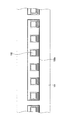
図5は、第1の実施形態に係る半導体発光素子アレイ装置を含む画像露光装置の構造を概略的に示す平面図である。図5に示される画像露光装置は、集積基板101上に複数の半導体発光素子薄膜102を1次元アレイ状に配列した構造を有する。この画像露光装置は、電子写真方式の画像形成装置において、感光体(図示せず)の表面に静電潜像を形成するための装置であり、例えば、LEDプリンタ用のLEDプリントヘッドである。なお、感光体(図示せず)の表面に形成された静電潜像は、現像装置(図示せず)によってトナー像となり、転写器(図示せず)によってトナー像を記録用紙に転写し、定着器(図示せず)による加熱及び加圧によってトナー像を記録用紙に定着させる。
FIG. 5 is a plan view schematically showing the structure of the image exposure apparatus including the semiconductor light emitting element array apparatus according to the first embodiment. The image exposure apparatus shown in FIG. 5 has a structure in which a plurality of semiconductor light emitting element
図6は、図5の要部P6の一例を拡大して示す平面図である。図6に示されるように、1次元アレイ状に複数の半導体発光素子薄膜102を集積基板101上に備える場合には、発光ドット毎に半導体発光素子薄膜102を形成し、1つのリムーバブル層108上に1つの半導体発光素子薄膜102を備えている。この場合には、半導体発光素子薄膜102を1個単位で交換可能である。
Figure 6 is an enlarged plan view showing an example of the main portion P 6 of FIG. As shown in FIG. 6, when a plurality of semiconductor light emitting element
また、図7は、図5の要部P7の他の例を拡大して示す平面図である。図7に示されるように、1次元アレイ状に複数の半導体発光素子薄膜102を集積基板101上に備える場合には、発光ドット毎に半導体発光素子薄膜102を形成し、1つのリムーバブル層108a上に複数の半導体発光素子薄膜102を備えてもよい。この場合には、半導体発光素子薄膜102を複数個単位(図7においては6個単位)で交換可能である。
7 is a plan view showing an enlarged another example of the main part P 7 of FIG. As shown in FIG. 7, when a plurality of semiconductor light emitting element
図8は、第1の実施形態に係る半導体発光素子アレイ装置を含む画像表示装置の構造を概略的に示す平面図であり、図9は、図8の要部P9の一例を拡大して示す平面図である。図8及び図9に示されるように、集積基板101上に複数の半導体発光素子薄膜102を二次元アレイ状に備えることより、LEDディスプレイなどの画像表示装置を構成することができる。まず、半導体発光素子薄膜102を集積基板101上に二次元アレイ状に取付け、集積基板101上に形成した上側電極共通配線121と半導体発光素子薄膜102上に形成した上側コンタクト層103とを上側電極接続配線131によって接続し、下側電極共通配線122と半導体発光素子薄膜102上に形成した下側電極パッド110とを下側電極接続配線132によって接続する。なお、上側電極共通配線121と上側電極接続配線131を一体形成することもでき、また、下側電極共通配線122と下側接続配線132は一体形成することもできる。
8, the structure of an image display device including a semiconductor light emitting device array according to the first embodiment is a plan view schematically illustrating, FIG. 9 is an enlarged example of a main part P 9 of FIG. 8 FIG. As shown in FIGS. 8 and 9, an image display device such as an LED display can be configured by providing a plurality of semiconductor light emitting element
図10(a)〜(d)は、第1の実施形態に係る半導体発光素子アレイ装置の不具合箇所の半導体発光素子薄膜の交換処理を示す平面図である。半導体発光素子薄膜102が、ケミカルエッチング困難な材料、例えば、AlxGa1−xAs、GaAs、(AlxGa1−x)yIn1−yP、GaN、AlGaN、及びInGaNのいずれかの材料により構成されている場合であっても、集積基板101と半導体発光素子薄膜102との間に、選択的にケミカルエッチング可能なリムーバブル層108を設けておくことにより、半導体発光素子薄膜102に位置ずれが生じた場合又は半導体発光素子薄膜102の形状に異常を確認した場合に、リムーバブル層108を選択的に除去することにより、その上層である半導体発光素子薄膜102を除去することができる。また、半導体発光素子薄膜102がケミカルエッチング可能な材料、例えば、GaAs又はAlxGa1−xAsで構成されている場合においても、接合により変質又は変形した接合面を除去するプロセスと並行して、半導体発光素子薄膜102を除去することができる。このような手法により半導体発光素子薄膜102を除去した場合には、集積基板102の表面(半導体発光素子薄膜102を除去した部分の表面)に平坦な状態が再現されるため、その上に、再度リムーバブル層108を形成し、さらにその上に、半導体発光素子薄膜102を密着固定することができる。
FIGS. 10A to 10D are plan views showing the replacement process of the semiconductor light emitting element thin film at the defective portion of the semiconductor light emitting element array device according to the first embodiment. The semiconductor light emitting device
例えば、図10(a)に示されるように、位置ずれが生じた半導体発光素子薄膜(「集積不良ドット」とも言う)141及び形状異常が生じた半導体発光素子薄膜(「外形不良ドット」とも言う)142と判定された半導体発光素子薄膜のポジションを確認する。次に、図10(b)に示されるように、ポジ型のフォトレジストで全体を覆い、図10(a)で確認した集積不良ドット141及び外形不良ドット142の領域のみスポット露光した後、現像する。この工程により図10(a)により確認した集積不良ドット141及び外形不良ドット142の領域のみ開口(開口部152)したマスクレジスト151を形成することができる。
For example, as shown in FIG. 10A, a semiconductor light emitting element thin film (also referred to as “integrated defective dot”) 141 in which a positional shift has occurred and a semiconductor light emitting element thin film in which a shape abnormality has occurred (also referred to as “externally defective dot”). ) The position of the semiconductor light emitting element thin film determined to be 142 is confirmed. Next, as shown in FIG. 10B, the whole is covered with a positive type photoresist, and only the areas of the
次に、リムーバブル層108のみを選択的にエッチング可能なエッチャントの中に、図10(b)により作製した構造体をディップ(浸漬)する。エッチャントとしては、リムーバブル層108がAl及びAl2O3で形成され、集積基板101又はパッシベーション膜(図示せず)がSiO2又はSiNを基本とする材料で構成されている場合は、85℃に熱したリン酸を用いることができる。また、リムーバブル層101がSiO2、SiN、及びTiなのいずれかの材料で構成され、集積基板101又はパッシベーション膜(図示せず)がAl2O3で形成されている場合には、エッチャントとして、緩衝HF(フッ酸系緩衝溶液)又はHFを用いることによりリムーバブル層108のみを選択的に除去することができる。リムーバブル層108を除去することによって、半導体発光素子薄膜が除去された状態は、図10(c)に示される。
Next, the structure manufactured according to FIG. 10B is dipped (immersed) in an etchant that can selectively etch only the
次に、マスクレジスト151を除去した後に、図10(d)に示されるように、半導体発光素子薄膜が除去された位置に、リムーバブル層108を再度形成する。最後に、図10(e)に示されるように、再度形成されたリムーバブル層108上に、半導体発光素子薄膜102を、取付ける。
Next, after removing the mask resist 151, as shown in FIG. 10D, the
以上に説明したように、第1の実施形態に係る半導体発光素子アレイ装置、画像露光装置、画像形成装置、及び画像表示装置においては、半導体発光素子アレイ装置の集積基板101と半導体発光素子薄膜102との間に、ケミカルエッチングにより選択的にエッチング可能なリムーバブル層108を設けているので、半導体発光素子薄膜102がケミカルエッチングの困難な材料から構成されている場合であっても、集積基板101の表面材料に損傷を与えずに、一旦固定された半導体発光素子薄膜102を集積基板101上から除去することが可能である。このため、集積基板101に固定された半導体発光素子薄膜102に接合不良や外形異常などの不具合が発見された場合には、不具合のある半導体発光素子薄膜のみを新しい半導体発光素子薄膜に交換することができ、最終的な完全良品の製造歩留まりを高めることができる。
As described above, in the semiconductor light emitting element array apparatus, the image exposure apparatus, the image forming apparatus, and the image display apparatus according to the first embodiment, the
第2の実施形態
図11は、本発明の第2の実施形態に係る半導体発光素子アレイ装置の要部の構造(配線層形成前)を概略的に示す縦断面図であり、図12は、図11の半導体発光素子アレイ装置の要部の構造を概略的に示す平面図である。なお、図11は、図12をS11−S11線で切る断面を示している。
Second Embodiment FIG. 11 is a longitudinal sectional view schematically showing a structure (before forming a wiring layer) of a main part of a semiconductor light emitting element array device according to a second embodiment of the present invention. FIG. 12 is a plan view schematically showing a structure of a main part of the semiconductor light emitting element array device of FIG. 11. FIG. 11 shows a cross section of FIG. 12 taken along line S 11 -S 11 .
第2の実施形態に係る半導体発光素子アレイ装置は、平坦化膜209が追加されている点において、第1の実施形態に係る半導体発光素子アレイ装置と相違する。第2の実施形態に係る半導体発光素子アレイ装置における集積基板201、リムーバブル層208、半導体発光素子薄膜202は、第1の実施形態に係る半導体発光素子アレイ装置における集積基板101、リムーバブル層108、半導体発光素子薄膜102とそれぞれ同様の構成を有している。また、第2の実施形態に係る半導体発光素子アレイ装置における上側コンタクト層203、上側クラッド層204、活性層205、下側クラッド層206、及び下側コンタクト層207は、第1の実施形態に係る半導体発光素子アレイ装置における上側コンタクト層103、上側クラッド層104、活性層105、下側クラッド層106、及び下側コンタクト層107とそれぞれ同様の構成を有している。
The semiconductor light emitting element array device according to the second embodiment is different from the semiconductor light emitting element array device according to the first embodiment in that a
平坦化膜209は、リムーバブル層208上に、表面ラフネスを小さくできる塗布工程により成膜可能であり、感光性又はドライエッチング性を有する有機絶縁膜、例えば、ポリイミド、アクリル、SOG(Spin On Glass)又はノボラックからなる形成される。平坦化膜209は、リムーバブル層208よりも小さく形成する必要があり、平坦化膜209が直接、集積基板201と接触しないように形成されている。なお、平坦化膜209の表面ラフネスは5nm以下であることが望ましい。平坦化膜209とその上の半導体発光素子薄膜202とは、分子間力接合、水素結合、陽極接合、又はエポキシなどによる接着剤により接合される。
The
図13は、第2の実施形態に係る半導体発光素子アレイ装置の要部の構造(配線層形成後)を概略的に示す縦断面図であり、図14は、図2の半導体発光素子アレイ装置の要部の構造を概略的に示す平面図である。なお、図13は、図14をS13−S13線で切る断面を示している。 13 is a longitudinal sectional view schematically showing the structure (after the wiring layer is formed) of the main part of the semiconductor light emitting element array device according to the second embodiment, and FIG. 14 is a semiconductor light emitting element array device of FIG. It is a top view which shows roughly the structure of the principal part. FIG. 13 shows a cross section of FIG. 14 taken along line S 13 -S 13 .
第2の実施形態に係る半導体発光素子アレイ装置における下側電極パッド210、上側電極接続配線211、下側電極接続配線212、及び層間絶縁膜213は、第1の実施形態に係る半導体発光素子アレイ装置における下側電極パッド110、上側電極接続配線111、下側電極接続配線112、及び層間絶縁膜113とそれぞれ同様の構成を有している。
The
第2の実施形態に係る半導体発光素子アレイ装置によれば、塗布工程により成膜可能な有機絶縁膜、例えば、ポリイミド、アクリル、SOG、又はノボラック、をリムーバブル層208上に形成することにより、リムーバブル層208上に形成される典型的な表面ラフネスよりも小さい表面ラフネスの平坦化層209を形成することができる。その結果、その上に形成される半導体発光素子薄膜102との間のより強固な分子間力接合、水素結合、陽極接合を得ることができる。また、公知の蒸着法又はスパッタ法を用いて形成するTi又はAlなどのメタル材料をリムーバブル層208に用いた場合、表面ラフネスを小さくすることは非常に困難であり、分子間力、水素結合又は陽極接合による集積が困難な場合がある。そのような場合においても、本発明による平坦化膜209をリムーバル層208と半導体発光素子薄膜202の間に挿入することにより、集積可能とすることができる。
According to the semiconductor light-emitting element array device according to the second embodiment, an organic insulating film that can be formed by a coating process, for example, polyimide, acrylic, SOG, or novolac, is formed on the
また、第2の実施形態に係る半導体発光素子アレイ装置においても、第1の実施形態に係る半導体発光素子アレイ装置と同様に、図10(a)〜(e)に示される手法により、不良ドットの修復を行うことができる。 Also, in the semiconductor light emitting element array device according to the second embodiment, as in the semiconductor light emitting element array device according to the first embodiment, defective dots are obtained by the method shown in FIGS. Can be repaired.
また、第2の実施形態に係る半導体発光素子アレイ装置を用いて、第1の実施形態の場合と同様に、画像露光装置、画像形成装置、及び画像表示装置を形成することができる。 In addition, an image exposure apparatus, an image forming apparatus, and an image display apparatus can be formed using the semiconductor light emitting element array apparatus according to the second embodiment, as in the case of the first embodiment.
以上に説明したように、第2の実施形態に係る半導体発光素子アレイ装置、画像露光装置、画像形成装置、及び画像表示装置においては、半導体発光素子アレイ装置の集積基板201と半導体発光素子薄膜202との間に、ケミカルエッチングにより選択的にエッチング可能なリムーバブル層208及び平坦化膜209を設けているので、半導体発光素子薄膜202がケミカルエッチングの困難な材料から構成されている場合であっても、集積基板201の表面材料に損傷を与えずに、一旦固定された半導体発光素子薄膜202を集積基板201上から除去することが可能である。このため、集積基板201に固定された半導体発光素子薄膜202に接合不良や外形異常などの不具合が発見された場合には、不具合のある半導体発光素子薄膜のみを新しい半導体発光素子薄膜に交換することができ、最終的な完全良品の製造歩留まりを高めることができる。
As described above, in the semiconductor light emitting element array apparatus, the image exposure apparatus, the image forming apparatus, and the image display apparatus according to the second embodiment, the
なお、第2の実施形態において、上記以外の点は、上記第1の実施形態の場合と同じである。 In the second embodiment, points other than those described above are the same as in the case of the first embodiment.
第3の実施形態
図15は、本発明の第3の実施形態に係る半導体発光素子アレイ装置の要部の構造(配線層形成前)を概略的に示す縦断面図であり、図16は、図15の半導体発光素子アレイ装置の要部の構造を概略的に示す平面図である。なお、図15は、図16をS15−S15線で切る断面を示している。
Third Embodiment FIG. 15 is a longitudinal sectional view schematically showing the structure of a main part (before forming a wiring layer) of a semiconductor light emitting element array device according to a third embodiment of the present invention. FIG. 16 is a plan view schematically showing a structure of a main part of the semiconductor light emitting element array device of FIG. 15. FIG. 15 shows a cross section of FIG. 16 taken along the line S 15 -S 15 .
第3の実施形態に係る半導体発光素子アレイ装置は、裏面電極層309が追加されている点において、第1の実施形態に係る半導体発光素子アレイ装置と相違する。第3の実施形態に係る半導体発光素子アレイ装置における集積基板301、リムーバブル層308、半導体発光素子薄膜302は、第1の実施形態に係る半導体発光素子アレイ装置における集積基板101、リムーバブル層108、半導体発光素子薄膜102とそれぞれ同様の構成を有している。また、第3の実施形態に係る半導体発光素子アレイ装置における上側コンタクト層303、上側クラッド層304、活性層305、下側クラッド層306、及び下側コンタクト層307は、第1の実施形態に係る半導体発光素子アレイ装置における上側コンタクト層103、上側クラッド層104、活性層105、下側クラッド層106、及び下側コンタクト層107とそれぞれ同様の構成を有している。
The semiconductor light emitting element array device according to the third embodiment is different from the semiconductor light emitting element array device according to the first embodiment in that a
裏面電極層309は、リムーバブル層308上に、半導体発光素子薄膜302における下側コンタクト層307と電気的に接触可能なメタル材料からなる電極層として形成されている。すなわち、半導体発光素子薄膜302の表面に上側電極が形成され、半導体発光素子薄膜302の裏面には下側電極が形成されている。したがって、半導体発光素子薄膜302は第1及び第2の実施形態に掲載したように下側コンタクト層307が露出するようなエッチング工程が必要無く、上側コンタクト層303、上側クラッド層304、活性層305、下側クラッド層306、及び下側コンタクト層307を同サイズにエッチング形成することができる。裏面電極層309のサイズは、リムーバブル層308よりも小さく形成されており、裏面電極層309は集積基板301と直接接触することのないように形成されている。なお、半導体発光素子薄膜302は分子間力接合、水素結合、陽極接合又は導電性を有する接着剤により該裏面電極層309上に集積化することができる。
The
図17は、第3の実施形態に係る半導体発光素子アレイ装置の要部の構造(配線層形成後)を概略的に示す縦断面図であり、図18は、図17の半導体発光素子アレイ装置の要部の構造を概略的に示す平面図である。なお、図17は、図18をS17−S17線で切る断面を示している。 FIG. 17 is a longitudinal sectional view schematically showing the structure (after the wiring layer is formed) of the main part of the semiconductor light emitting element array device according to the third embodiment, and FIG. 18 is the semiconductor light emitting element array device of FIG. It is a top view which shows roughly the structure of the principal part. FIG. 17 shows a cross section of FIG. 18 taken along line S 17 -S 17 .
第3の実施形態に係る半導体発光素子アレイ装置における上側電極接続配線311、下側電極接続配線312、及び層間絶縁膜313は、第1の実施形態に係る半導体発光素子アレイ装置における上側電極接続配線111、下側電極接続配線112、及び層間絶縁膜113とそれぞれ同様の構成を有している。
The upper
第3の実施形態に係る半導体発光素子アレイ装置によれば、集積面を下側コンタクト層307と電気的に接触可能なメタル材料からなる裏面電極層309とすることにより、半導体発光素子薄膜302の下側電極を、半導体発光素子薄膜302の裏面に形成することが可能となる。そのため、半導体発光素子薄膜の構造を簡略化することができ、半導体発光素子薄膜のシュリンクが可能となる。
According to the semiconductor light emitting element array device according to the third embodiment, the integration surface is the
また、第3の実施形態に係る半導体発光素子アレイ装置においても、第1の実施形態に係る半導体発光素子アレイ装置と同様に、図10(a)〜(e)に示される手法により、不良ドットの修復を行うことができる。 Further, in the semiconductor light emitting element array device according to the third embodiment, as in the semiconductor light emitting element array device according to the first embodiment, defective dots are obtained by the method shown in FIGS. Can be repaired.
また、第3の実施形態に係る半導体発光素子アレイ装置を用いて、第1の実施形態の場合と同様に、画像露光装置、画像形成装置、及び画像表示装置を形成することができる。 In addition, an image exposure apparatus, an image forming apparatus, and an image display apparatus can be formed using the semiconductor light emitting element array apparatus according to the third embodiment, as in the case of the first embodiment.
以上に説明したように、第3の実施形態に係る半導体発光素子アレイ装置、画像露光装置、画像形成装置、及び画像表示装置においては、半導体発光素子アレイ装置の集積基板301と半導体発光素子薄膜302下の裏面電極層309との間に、ケミカルエッチングにより選択的にエッチング可能なリムーバブル層308を設けているので、半導体発光素子薄膜302がケミカルエッチングの困難な材料から構成されている場合であっても、集積基板301の表面材料に損傷を与えずに、一旦固定された半導体発光素子薄膜302を集積基板301上から除去することが可能である。このため、集積基板301に固定された半導体発光素子薄膜302に接合不良や外形異常などの不具合が発見された場合には、不具合のある半導体発光素子薄膜のみを新しい半導体発光素子薄膜に交換することができ、最終的な完全良品の製造歩留まりを高めることができる。
As described above, in the semiconductor light emitting element array apparatus, the image exposure apparatus, the image forming apparatus, and the image display apparatus according to the third embodiment, the
なお、第3の実施形態において、上記以外の点は、上記第1又は第2の実施形態の場合と同じである。 In the third embodiment, points other than the above are the same as those in the first or second embodiment.
101,201,301 集積基板、
102,202,302 半導体発光素子薄膜、
103,203,303 上側コンタクト層、
104,204,304 上側クラッド層、
105,205,305 活性層、
106,206,306 下側クラッド層、
107,207,307 下側コンタクト層、
108,208,308 リムーバブル層、
209 平坦化膜、
309 裏面電極層、
110,210 下側電極パッド、
111,211,311 上側電極接続配線、
112,212,312 下側電極接続配線、
113,213,313 層間絶縁膜。
101, 201, 301 integrated substrate,
102, 202, 302 Semiconductor light emitting device thin film,
103, 203, 303 upper contact layer,
104, 204, 304 upper cladding layer,
105, 205, 305 active layer,
106, 206, 306 lower clad layer,
107,207,307 Lower contact layer,
108, 208, 308 removable layer,
209 planarization film,
309 back electrode layer,
110, 210 Lower electrode pad,
111, 211, 311 Upper electrode connection wiring,
112, 212, 312 Lower electrode connection wiring,
113, 213, 313 Interlayer insulating film.
Claims (15)
前記基板上に備えられた複数のリムーバブル層と、
前記複数のリムーバブル層上に備えられ、前記基板の表面材料とは異なる材料から構成され、半導体発光素子を備える半導体発光素子薄膜とを有し、
前記複数のリムーバブル層は、ケミカルエッチングによって前記基板に対して選択的にエッチング可能な材料で構成され、前記複数のリムーバブル層のそれぞれの上には、前記半導体発光素子薄膜が1つ設けられる
ことを特徴とする半導体発光素子アレイ装置。 A substrate,
A plurality of removable layers provided on the substrate;
A semiconductor light-emitting element thin film provided on the plurality of removable layers, made of a material different from the surface material of the substrate, and comprising a semiconductor light-emitting element;
Wherein the plurality of removable layers are selectively configured in etchable material to the substrate by chemical etching, on each of said plurality of removable layers, said semiconductor light emitting element thin film Ru provided one A semiconductor light-emitting element array device.
前記複数のリムーバブル層は、Al、Al2O3のいずれかの材料によって形成されている
ことを特徴とする請求項1に記載の半導体発光素子アレイ装置。 The surface material of the substrate is formed of any material of SiO 2 , SiN, Ti,
2. The semiconductor light emitting element array device according to claim 1, wherein the plurality of removable layers are formed of any one of Al and Al 2 O 3 .
前記複数のリムーバブル層は、SiO2、SiN、Tiのいずれかの材料によって形成されている
ことを特徴とする請求項1に記載の半導体発光素子アレイ装置。 The surface material of the substrate is formed of any one of Al and Al 2 O 3 ,
The semiconductor light emitting element array device according to claim 1, wherein the plurality of removable layers are formed of any one of SiO 2 , SiN, and Ti.
前記半導体発光素子薄膜は、前記平坦化層上に分子間力、水素結合、接着剤のいずれかにより固定されている
ことを特徴とする請求項1乃至4のいずれか1項に記載の半導体発光素子アレイ装置。 Further comprising a planarization layer provided on the removable layer;
5. The semiconductor light-emitting device according to claim 1, wherein the semiconductor light-emitting element thin film is fixed on the planarizing layer by any of intermolecular force, hydrogen bond, and adhesive. Element array device.
前記基板上に備えられた複数のリムーバブル層と、
前記リムーバブル層上に備えられた裏面電極層と、
前記裏面電極層上に備えられ、前記基板の表面材料とは異なる材料から構成され、半導体発光素子を備える半導体発光素子薄膜とを有し、
前記複数のリムーバブル層は、ケミカルエッチングによって選択的にエッチング可能な材料で構成され、
前記半導体発光素子薄膜は、前記裏面電極層上に分子間力、水素結合、陽極接合、接着剤のいずれかにより固定されている
ことを特徴とする半導体発光素子アレイ装置。 A substrate,
A plurality of removable layers provided on the substrate;
A back electrode layer provided on the removable layer;
A semiconductor light-emitting element thin film comprising a semiconductor light-emitting element, comprising a material different from the surface material of the substrate, provided on the back electrode layer;
The plurality of removable layers are made of a material that can be selectively etched by chemical etching ,
The semiconductor light-emitting element thin film is fixed on the back electrode layer by intermolecular force, hydrogen bonding, anodic bonding, or adhesive .
前記発光素子アレイは、
基板と、
前記基板上に備えられた複数のリムーバブル層と、
前記複数のリムーバブル層上に備えられ、前記基板の表面材料とは異なる材料から構成され、半導体発光素子を備える半導体発光素子薄膜とを有し、
前記複数のリムーバブル層は、ケミカルエッチングによって前記基板に対して選択的にエッチング可能な材料で構成され、前記複数のリムーバブル層のそれぞれの上には、前記半導体発光素子薄膜が1つ設けられる
ことを特徴とする画像露光装置。 An image exposure apparatus having an image exposure unit including a semiconductor light emitting element array,
The light emitting element array is:
A substrate,
A plurality of removable layers provided on the substrate;
A semiconductor light-emitting element thin film provided on the plurality of removable layers, made of a material different from the surface material of the substrate, and comprising a semiconductor light-emitting element;
Wherein the plurality of removable layers are selectively configured in etchable material to the substrate by chemical etching, on each of said plurality of removable layers, said semiconductor light emitting element thin film Ru provided one An image exposure apparatus.
前記発光素子アレイは、
基板と、
前記基板上に備えられた複数のリムーバブル層と、
前記複数のリムーバブル層上に備えられ、前記基板の表面材料とは異なる材料から構成され、半導体発光素子を備える半導体発光素子薄膜とを有し、
前記複数のリムーバブル層は、ケミカルエッチングによって前記基板に対して選択的にエッチング可能な材料で構成され、前記複数のリムーバブル層のそれぞれの上には、前記半導体発光素子薄膜が1つ設けられる
ことを特徴とする画像形成装置。 An image exposure apparatus having an image exposure unit having an image exposure unit including a semiconductor light emitting element array, and a photoreceptor on which an electrostatic latent image is formed by the image exposure apparatus,
The light emitting element array is:
A substrate,
A plurality of removable layers provided on the substrate;
A semiconductor light-emitting element thin film provided on the plurality of removable layers, made of a material different from the surface material of the substrate, and comprising a semiconductor light-emitting element;
Wherein the plurality of removable layers are selectively configured in etchable material to the substrate by chemical etching, on each of said plurality of removable layers, said semiconductor light emitting element thin film Ru provided one An image forming apparatus.
前記発光素子アレイは、
基板と、
前記基板上に備えられた複数のリムーバブル層と、
前記複数のリムーバブル層上に備えられ、前記基板の表面材料とは異なる材料から構成され、半導体発光素子を備える半導体発光素子薄膜とを有し、
前記複数のリムーバブル層は、ケミカルエッチングによって前記基板に対して選択的にエッチング可能な材料で構成され、前記複数のリムーバブル層のそれぞれの上には、前記半導体発光素子薄膜が1つ設けられる
ことを特徴とする画像表示装置。 An image display device having an image display unit including a semiconductor light emitting element array,
The light emitting element array is:
A substrate,
A plurality of removable layers provided on the substrate;
A semiconductor light-emitting element thin film provided on the plurality of removable layers, made of a material different from the surface material of the substrate, and comprising a semiconductor light-emitting element;
Wherein the plurality of removable layers are selectively configured in etchable material to the substrate by chemical etching, on each of said plurality of removable layers, said semiconductor light emitting element thin film Ru provided one An image display device characterized by the above.
前記発光素子アレイは、 The light emitting element array is:
基板と、 A substrate,
前記基板上に備えられた複数のリムーバブル層と、 A plurality of removable layers provided on the substrate;
前記リムーバブル層上に備えられた裏面電極層と、 A back electrode layer provided on the removable layer;
前記裏面電極層上に備えられ、前記基板の表面材料とは異なる材料から構成され、半導体発光素子を備える半導体発光素子薄膜とを有し、 A semiconductor light-emitting element thin film comprising a semiconductor light-emitting element, comprising a material different from the surface material of the substrate, provided on the back electrode layer;
前記複数のリムーバブル層は、ケミカルエッチングによって選択的にエッチング可能な材料で構成され、 The plurality of removable layers are made of a material that can be selectively etched by chemical etching,
前記半導体発光素子薄膜は、前記裏面電極層上に分子間力、水素結合、陽極接合、接着剤のいずれかにより固定されている The semiconductor light emitting device thin film is fixed on the back electrode layer by any of intermolecular force, hydrogen bonding, anodic bonding, and adhesive.
ことを特徴とする画像露光装置。 An image exposure apparatus characterized by that.
前記発光素子アレイは、 The light emitting element array is:
基板と、 A substrate,
前記基板上に備えられた複数のリムーバブル層と、 A plurality of removable layers provided on the substrate;
前記リムーバブル層上に備えられた裏面電極層と、 A back electrode layer provided on the removable layer;
前記裏面電極層上に備えられ、前記基板の表面材料とは異なる材料から構成され、半導体発光素子を備える半導体発光素子薄膜とを有し、 A semiconductor light-emitting element thin film comprising a semiconductor light-emitting element, comprising a material different from the surface material of the substrate, provided on the back electrode layer;
前記複数のリムーバブル層は、ケミカルエッチングによって選択的にエッチング可能な材料で構成され、 The plurality of removable layers are made of a material that can be selectively etched by chemical etching,
前記半導体発光素子薄膜は、前記裏面電極層上に分子間力、水素結合、陽極接合、接着剤のいずれかにより固定されている The semiconductor light emitting device thin film is fixed on the back electrode layer by any of intermolecular force, hydrogen bonding, anodic bonding, and adhesive.
ことを特徴とする画像形成装置。 An image forming apparatus.
前記発光素子アレイは、 The light emitting element array is:
基板と、 A substrate,
前記基板上に備えられた複数のリムーバブル層と、 A plurality of removable layers provided on the substrate;
前記リムーバブル層上に備えられた裏面電極層と、 A back electrode layer provided on the removable layer;
前記裏面電極層上に備えられ、前記基板の表面材料とは異なる材料から構成され、半導体発光素子を備える半導体発光素子薄膜とを有し、 A semiconductor light-emitting element thin film comprising a semiconductor light-emitting element, comprising a material different from the surface material of the substrate, provided on the back electrode layer;
前記複数のリムーバブル層は、ケミカルエッチングによって選択的にエッチング可能な材料で構成され、 The plurality of removable layers are made of a material that can be selectively etched by chemical etching,
前記半導体発光素子薄膜は、前記裏面電極層上に分子間力、水素結合、陽極接合、接着剤のいずれかにより固定されている The semiconductor light emitting device thin film is fixed on the back electrode layer by any of intermolecular force, hydrogen bonding, anodic bonding, and adhesive.
ことを特徴とする画像表示装置。 An image display device characterized by that.
Priority Applications (2)
| Application Number | Priority Date | Filing Date | Title |
|---|---|---|---|
| JP2009193065A JP4871378B2 (en) | 2009-08-24 | 2009-08-24 | Semiconductor light emitting element array apparatus, image exposure apparatus, image forming apparatus, and image display apparatus |
| US12/805,618 US20110042689A1 (en) | 2009-08-24 | 2010-08-10 | Semiconductor light-emitting element array device, image exposing device, image forming apparatus, and image display apparatus |
Applications Claiming Priority (1)
| Application Number | Priority Date | Filing Date | Title |
|---|---|---|---|
| JP2009193065A JP4871378B2 (en) | 2009-08-24 | 2009-08-24 | Semiconductor light emitting element array apparatus, image exposure apparatus, image forming apparatus, and image display apparatus |
Publications (3)
| Publication Number | Publication Date |
|---|---|
| JP2011044643A JP2011044643A (en) | 2011-03-03 |
| JP2011044643A5 JP2011044643A5 (en) | 2011-06-16 |
| JP4871378B2 true JP4871378B2 (en) | 2012-02-08 |
Family
ID=43604605
Family Applications (1)
| Application Number | Title | Priority Date | Filing Date |
|---|---|---|---|
| JP2009193065A Active JP4871378B2 (en) | 2009-08-24 | 2009-08-24 | Semiconductor light emitting element array apparatus, image exposure apparatus, image forming apparatus, and image display apparatus |
Country Status (2)
| Country | Link |
|---|---|
| US (1) | US20110042689A1 (en) |
| JP (1) | JP4871378B2 (en) |
Families Citing this family (5)
| Publication number | Priority date | Publication date | Assignee | Title |
|---|---|---|---|---|
| JP5584645B2 (en) * | 2011-03-31 | 2014-09-03 | 株式会社沖データ | Semiconductor light emitting device and head mounted display device |
| US9773945B2 (en) * | 2015-01-30 | 2017-09-26 | Osram Opto Semiconductors Gmbh | Method for producing a semiconductor component and a semiconductor component |
| JP6289718B1 (en) * | 2017-01-02 | 2018-03-07 | ルーメンス カンパニー リミテッド | LED display device |
| CN107611243B (en) * | 2017-09-26 | 2024-03-26 | 利亚德光电股份有限公司 | Display unit and display device |
| JP7469150B2 (en) | 2020-06-18 | 2024-04-16 | 豊田合成株式会社 | Light emitting element |
Family Cites Families (10)
| Publication number | Priority date | Publication date | Assignee | Title |
|---|---|---|---|---|
| JPS63237968A (en) * | 1987-03-26 | 1988-10-04 | Nec Corp | Light-emitting diode printer head |
| JPH05235257A (en) * | 1992-02-21 | 1993-09-10 | Hitachi Ltd | Semiconductor device and manufacture thereof |
| US7408566B2 (en) * | 2003-10-22 | 2008-08-05 | Oki Data Corporation | Semiconductor device, LED print head and image-forming apparatus using same, and method of manufacturing semiconductor device |
| US7932111B2 (en) * | 2005-02-23 | 2011-04-26 | Cree, Inc. | Substrate removal process for high light extraction LEDs |
| US20070069225A1 (en) * | 2005-09-27 | 2007-03-29 | Lumileds Lighting U.S., Llc | III-V light emitting device |
| JP2008060222A (en) * | 2006-08-30 | 2008-03-13 | Seiko Epson Corp | Device and method for driving light-emitting element |
| JP4279304B2 (en) * | 2006-08-31 | 2009-06-17 | 株式会社沖データ | Semiconductor device, LED print head, and image forming apparatus |
| JP2008263126A (en) * | 2007-04-13 | 2008-10-30 | Oki Data Corp | Semiconductor apparatus, method of manufacturing the same, led head, and image formation apparatus |
| KR101634970B1 (en) * | 2007-05-18 | 2016-06-30 | 가부시키가이샤 한도오따이 에네루기 켄큐쇼 | Semiconductor device and method for manufacturing the same |
| JP2009147352A (en) * | 2009-01-19 | 2009-07-02 | Oki Data Corp | Semiconductor apparatus, led head, and image forming apparatus |
-
2009
- 2009-08-24 JP JP2009193065A patent/JP4871378B2/en active Active
-
2010
- 2010-08-10 US US12/805,618 patent/US20110042689A1/en not_active Abandoned
Also Published As
| Publication number | Publication date |
|---|---|
| JP2011044643A (en) | 2011-03-03 |
| US20110042689A1 (en) | 2011-02-24 |
Similar Documents
| Publication | Publication Date | Title |
|---|---|---|
| JP5599916B2 (en) | Semiconductor device manufacturing method, semiconductor device, optical print head using the same, and image forming apparatus | |
| JP5415191B2 (en) | Semiconductor composite device, optical print head, and image forming apparatus | |
| TWI387129B (en) | Semiconductor member, semiconductor article manufacturing method, and led array using the manufacturing method | |
| US8420501B2 (en) | Transfer method of functional region, LED array, LED printer head, and LED printer | |
| KR101168881B1 (en) | Transfer method of functional region, led array, led printer head, and led printer | |
| JP5390832B2 (en) | Functional area transfer method, LED array, LED printer head, and LED printer | |
| JP2008147608A (en) | Method of manufacturing led array, led array, and led printer | |
| JP2010205943A (en) | Transfer method of functional region, led array, led printer head, and led printer | |
| JP4871378B2 (en) | Semiconductor light emitting element array apparatus, image exposure apparatus, image forming apparatus, and image display apparatus | |
| US7049207B2 (en) | Isolating method and transferring method for semiconductor devices | |
| JP2004179641A (en) | Semiconductor device, optical print head and image forming apparatus | |
| JP2004179646A (en) | Semiconductor composite device, optical print head and image forming apparatus | |
| JP5444141B2 (en) | Semiconductor light emitting device, image exposure apparatus, image forming apparatus, and image display apparatus | |
| JP6097682B2 (en) | Semiconductor light emitting device, image forming apparatus, image display device, and method for manufacturing semiconductor light emitting device | |
| JP2010056194A (en) | Semiconductor device and optical print head | |
| JP2010056193A (en) | Semiconductor device |
Legal Events
| Date | Code | Title | Description |
|---|---|---|---|
| A621 | Written request for application examination |
Free format text: JAPANESE INTERMEDIATE CODE: A621 Effective date: 20110310 |
|
| A521 | Request for written amendment filed |
Free format text: JAPANESE INTERMEDIATE CODE: A523 Effective date: 20110421 |
|
| A977 | Report on retrieval |
Free format text: JAPANESE INTERMEDIATE CODE: A971007 Effective date: 20110608 |
|
| A131 | Notification of reasons for refusal |
Free format text: JAPANESE INTERMEDIATE CODE: A131 Effective date: 20110621 |
|
| A521 | Request for written amendment filed |
Free format text: JAPANESE INTERMEDIATE CODE: A523 Effective date: 20110708 |
|
| TRDD | Decision of grant or rejection written | ||
| A01 | Written decision to grant a patent or to grant a registration (utility model) |
Free format text: JAPANESE INTERMEDIATE CODE: A01 Effective date: 20111108 |
|
| A01 | Written decision to grant a patent or to grant a registration (utility model) |
Free format text: JAPANESE INTERMEDIATE CODE: A01 |
|
| A61 | First payment of annual fees (during grant procedure) |
Free format text: JAPANESE INTERMEDIATE CODE: A61 Effective date: 20111118 |
|
| R150 | Certificate of patent or registration of utility model |
Ref document number: 4871378 Country of ref document: JP Free format text: JAPANESE INTERMEDIATE CODE: R150 Free format text: JAPANESE INTERMEDIATE CODE: R150 |
|
| FPAY | Renewal fee payment (event date is renewal date of database) |
Free format text: PAYMENT UNTIL: 20141125 Year of fee payment: 3 |
|
| S111 | Request for change of ownership or part of ownership |
Free format text: JAPANESE INTERMEDIATE CODE: R313115 |
|
| R350 | Written notification of registration of transfer |
Free format text: JAPANESE INTERMEDIATE CODE: R350 |
|
| S111 | Request for change of ownership or part of ownership |
Free format text: JAPANESE INTERMEDIATE CODE: R313111 |
|
| R350 | Written notification of registration of transfer |
Free format text: JAPANESE INTERMEDIATE CODE: R350 |