JP4865678B2 - Dielectric composite and method for manufacturing dielectric composite - Google Patents
Dielectric composite and method for manufacturing dielectric composite Download PDFInfo
- Publication number
- JP4865678B2 JP4865678B2 JP2007287670A JP2007287670A JP4865678B2 JP 4865678 B2 JP4865678 B2 JP 4865678B2 JP 2007287670 A JP2007287670 A JP 2007287670A JP 2007287670 A JP2007287670 A JP 2007287670A JP 4865678 B2 JP4865678 B2 JP 4865678B2
- Authority
- JP
- Japan
- Prior art keywords
- composite
- thin film
- conductive layer
- composite according
- transducer
- Prior art date
- Legal status (The legal status is an assumption and is not a legal conclusion. Google has not performed a legal analysis and makes no representation as to the accuracy of the status listed.)
- Active
Links
- 239000002131 composite material Substances 0.000 title claims abstract description 326
- 238000000034 method Methods 0.000 title description 34
- 238000004519 manufacturing process Methods 0.000 title description 27
- 239000003989 dielectric material Substances 0.000 claims abstract description 31
- 239000010409 thin film Substances 0.000 claims description 182
- 230000005684 electric field Effects 0.000 claims description 82
- 230000009975 flexible effect Effects 0.000 claims description 51
- 229920001971 elastomer Polymers 0.000 claims description 24
- 239000000806 elastomer Substances 0.000 claims description 24
- 238000005452 bending Methods 0.000 claims description 17
- 239000002861 polymer material Substances 0.000 claims 1
- 238000013461 design Methods 0.000 abstract description 35
- 230000000994 depressogenic effect Effects 0.000 abstract 1
- 239000010410 layer Substances 0.000 description 208
- 229910052751 metal Inorganic materials 0.000 description 44
- 239000002184 metal Substances 0.000 description 44
- 229920000642 polymer Polymers 0.000 description 31
- 230000004044 response Effects 0.000 description 31
- 239000000463 material Substances 0.000 description 27
- 238000004804 winding Methods 0.000 description 20
- 239000000853 adhesive Substances 0.000 description 19
- 230000001070 adhesive effect Effects 0.000 description 19
- 230000008569 process Effects 0.000 description 16
- 238000000576 coating method Methods 0.000 description 15
- 230000033001 locomotion Effects 0.000 description 15
- 239000003990 capacitor Substances 0.000 description 13
- 239000011248 coating agent Substances 0.000 description 13
- 239000010408 film Substances 0.000 description 13
- XKRFYHLGVUSROY-UHFFFAOYSA-N Argon Chemical compound [Ar] XKRFYHLGVUSROY-UHFFFAOYSA-N 0.000 description 12
- 230000007547 defect Effects 0.000 description 12
- 239000004033 plastic Substances 0.000 description 11
- 229920003023 plastic Polymers 0.000 description 11
- PXHVJJICTQNCMI-UHFFFAOYSA-N Nickel Chemical compound [Ni] PXHVJJICTQNCMI-UHFFFAOYSA-N 0.000 description 10
- 238000009826 distribution Methods 0.000 description 10
- 230000015556 catabolic process Effects 0.000 description 9
- 210000002381 plasma Anatomy 0.000 description 8
- XUIMIQQOPSSXEZ-UHFFFAOYSA-N Silicon Chemical compound [Si] XUIMIQQOPSSXEZ-UHFFFAOYSA-N 0.000 description 6
- 229910052786 argon Inorganic materials 0.000 description 6
- 239000004020 conductor Substances 0.000 description 6
- 230000006378 damage Effects 0.000 description 6
- 230000000694 effects Effects 0.000 description 6
- 238000004049 embossing Methods 0.000 description 6
- 239000007788 liquid Substances 0.000 description 6
- 229920002120 photoresistant polymer Polymers 0.000 description 6
- 230000036316 preload Effects 0.000 description 6
- 238000012545 processing Methods 0.000 description 6
- 229910052710 silicon Inorganic materials 0.000 description 6
- 239000010703 silicon Substances 0.000 description 6
- 239000012790 adhesive layer Substances 0.000 description 5
- 238000013459 approach Methods 0.000 description 5
- 230000008901 benefit Effects 0.000 description 5
- 239000007772 electrode material Substances 0.000 description 5
- 229910052759 nickel Inorganic materials 0.000 description 5
- 238000005240 physical vapour deposition Methods 0.000 description 5
- 238000001020 plasma etching Methods 0.000 description 5
- 238000005096 rolling process Methods 0.000 description 5
- BQCADISMDOOEFD-UHFFFAOYSA-N Silver Chemical compound [Ag] BQCADISMDOOEFD-UHFFFAOYSA-N 0.000 description 4
- 239000000956 alloy Substances 0.000 description 4
- 229910045601 alloy Inorganic materials 0.000 description 4
- 238000006243 chemical reaction Methods 0.000 description 4
- 230000006835 compression Effects 0.000 description 4
- 238000007906 compression Methods 0.000 description 4
- PCHJSUWPFVWCPO-UHFFFAOYSA-N gold Chemical compound [Au] PCHJSUWPFVWCPO-UHFFFAOYSA-N 0.000 description 4
- 239000010931 gold Substances 0.000 description 4
- 229910052737 gold Inorganic materials 0.000 description 4
- 238000000465 moulding Methods 0.000 description 4
- 229910052709 silver Inorganic materials 0.000 description 4
- 239000004332 silver Substances 0.000 description 4
- 239000003351 stiffener Substances 0.000 description 4
- 239000000725 suspension Substances 0.000 description 4
- OKTJSMMVPCPJKN-UHFFFAOYSA-N Carbon Chemical compound [C] OKTJSMMVPCPJKN-UHFFFAOYSA-N 0.000 description 3
- 239000002318 adhesion promoter Substances 0.000 description 3
- 229910052799 carbon Inorganic materials 0.000 description 3
- 238000001723 curing Methods 0.000 description 3
- 238000010586 diagram Methods 0.000 description 3
- 239000013536 elastomeric material Substances 0.000 description 3
- 239000007789 gas Substances 0.000 description 3
- 239000004519 grease Substances 0.000 description 3
- 238000000025 interference lithography Methods 0.000 description 3
- 238000003475 lamination Methods 0.000 description 3
- 238000000608 laser ablation Methods 0.000 description 3
- 238000001459 lithography Methods 0.000 description 3
- 230000007246 mechanism Effects 0.000 description 3
- 238000009832 plasma treatment Methods 0.000 description 3
- 230000010076 replication Effects 0.000 description 3
- 230000002441 reversible effect Effects 0.000 description 3
- KRHYYFGTRYWZRS-UHFFFAOYSA-N Fluorane Chemical compound F KRHYYFGTRYWZRS-UHFFFAOYSA-N 0.000 description 2
- 239000002313 adhesive film Substances 0.000 description 2
- QVGXLLKOCUKJST-UHFFFAOYSA-N atomic oxygen Chemical compound [O] QVGXLLKOCUKJST-UHFFFAOYSA-N 0.000 description 2
- 239000011247 coating layer Substances 0.000 description 2
- 238000000151 deposition Methods 0.000 description 2
- 238000006073 displacement reaction Methods 0.000 description 2
- 239000011521 glass Substances 0.000 description 2
- 238000010030 laminating Methods 0.000 description 2
- 239000011344 liquid material Substances 0.000 description 2
- 238000011068 loading method Methods 0.000 description 2
- 150000002739 metals Chemical class 0.000 description 2
- 239000000203 mixture Substances 0.000 description 2
- 210000003205 muscle Anatomy 0.000 description 2
- 238000005457 optimization Methods 0.000 description 2
- 238000013021 overheating Methods 0.000 description 2
- 229910052760 oxygen Inorganic materials 0.000 description 2
- 239000001301 oxygen Substances 0.000 description 2
- 230000000737 periodic effect Effects 0.000 description 2
- -1 polyethylene Polymers 0.000 description 2
- 239000000047 product Substances 0.000 description 2
- 238000003380 quartz crystal microbalance Methods 0.000 description 2
- 230000035484 reaction time Effects 0.000 description 2
- 238000007493 shaping process Methods 0.000 description 2
- 238000004088 simulation Methods 0.000 description 2
- 239000007787 solid Substances 0.000 description 2
- 238000004528 spin coating Methods 0.000 description 2
- 238000005507 spraying Methods 0.000 description 2
- 238000004544 sputter deposition Methods 0.000 description 2
- 239000000758 substrate Substances 0.000 description 2
- 230000001052 transient effect Effects 0.000 description 2
- 235000012431 wafers Nutrition 0.000 description 2
- 229920000049 Carbon (fiber) Polymers 0.000 description 1
- VYZAMTAEIAYCRO-UHFFFAOYSA-N Chromium Chemical compound [Cr] VYZAMTAEIAYCRO-UHFFFAOYSA-N 0.000 description 1
- BPQQTUXANYXVAA-UHFFFAOYSA-N Orthosilicate Chemical compound [O-][Si]([O-])([O-])[O-] BPQQTUXANYXVAA-UHFFFAOYSA-N 0.000 description 1
- 239000004698 Polyethylene Substances 0.000 description 1
- RTAQQCXQSZGOHL-UHFFFAOYSA-N Titanium Chemical compound [Ti] RTAQQCXQSZGOHL-UHFFFAOYSA-N 0.000 description 1
- 229920000800 acrylic rubber Polymers 0.000 description 1
- 239000002390 adhesive tape Substances 0.000 description 1
- 230000015572 biosynthetic process Effects 0.000 description 1
- 239000004917 carbon fiber Substances 0.000 description 1
- OKTJSMMVPCPJKN-YPZZEJLDSA-N carbon-10 atom Chemical compound [10C] OKTJSMMVPCPJKN-YPZZEJLDSA-N 0.000 description 1
- 238000005266 casting Methods 0.000 description 1
- 230000008859 change Effects 0.000 description 1
- 238000004140 cleaning Methods 0.000 description 1
- 239000013065 commercial product Substances 0.000 description 1
- 238000010924 continuous production Methods 0.000 description 1
- 230000008878 coupling Effects 0.000 description 1
- 238000010168 coupling process Methods 0.000 description 1
- 238000005859 coupling reaction Methods 0.000 description 1
- 238000005336 cracking Methods 0.000 description 1
- 238000004132 cross linking Methods 0.000 description 1
- 238000005520 cutting process Methods 0.000 description 1
- 230000007423 decrease Effects 0.000 description 1
- 230000032798 delamination Effects 0.000 description 1
- 230000001419 dependent effect Effects 0.000 description 1
- 230000008021 deposition Effects 0.000 description 1
- 238000011161 development Methods 0.000 description 1
- 238000007598 dipping method Methods 0.000 description 1
- 230000009977 dual effect Effects 0.000 description 1
- 239000002305 electric material Substances 0.000 description 1
- 238000010292 electrical insulation Methods 0.000 description 1
- 238000010894 electron beam technology Methods 0.000 description 1
- 238000009713 electroplating Methods 0.000 description 1
- 238000005530 etching Methods 0.000 description 1
- 230000008020 evaporation Effects 0.000 description 1
- 238000001704 evaporation Methods 0.000 description 1
- 239000012467 final product Substances 0.000 description 1
- 239000011888 foil Substances 0.000 description 1
- 238000013007 heat curing Methods 0.000 description 1
- 150000002500 ions Chemical class 0.000 description 1
- 238000000691 measurement method Methods 0.000 description 1
- VNWKTOKETHGBQD-UHFFFAOYSA-N methane Chemical compound C VNWKTOKETHGBQD-UHFFFAOYSA-N 0.000 description 1
- 239000012778 molding material Substances 0.000 description 1
- 239000002071 nanotube Substances 0.000 description 1
- 238000010899 nucleation Methods 0.000 description 1
- 230000003287 optical effect Effects 0.000 description 1
- 230000003647 oxidation Effects 0.000 description 1
- 238000007254 oxidation reaction Methods 0.000 description 1
- 239000012785 packaging film Substances 0.000 description 1
- 229920006280 packaging film Polymers 0.000 description 1
- 238000010422 painting Methods 0.000 description 1
- 238000007591 painting process Methods 0.000 description 1
- 239000002245 particle Substances 0.000 description 1
- 230000000149 penetrating effect Effects 0.000 description 1
- 229920000058 polyacrylate Polymers 0.000 description 1
- 229920000573 polyethylene Polymers 0.000 description 1
- 238000005381 potential energy Methods 0.000 description 1
- 238000002360 preparation method Methods 0.000 description 1
- 238000003825 pressing Methods 0.000 description 1
- 238000003672 processing method Methods 0.000 description 1
- 238000000746 purification Methods 0.000 description 1
- 239000011347 resin Substances 0.000 description 1
- 229920005989 resin Polymers 0.000 description 1
- 239000011265 semifinished product Substances 0.000 description 1
- 229920002379 silicone rubber Polymers 0.000 description 1
- 238000007764 slot die coating Methods 0.000 description 1
- 239000007779 soft material Substances 0.000 description 1
- 239000002904 solvent Substances 0.000 description 1
- 230000006641 stabilisation Effects 0.000 description 1
- 238000011105 stabilization Methods 0.000 description 1
- 230000000638 stimulation Effects 0.000 description 1
- TXEYQDLBPFQVAA-UHFFFAOYSA-N tetrafluoromethane Chemical compound FC(F)(F)F TXEYQDLBPFQVAA-UHFFFAOYSA-N 0.000 description 1
- 239000010936 titanium Substances 0.000 description 1
- 229910052719 titanium Inorganic materials 0.000 description 1
- 238000001771 vacuum deposition Methods 0.000 description 1
- 238000007740 vapor deposition Methods 0.000 description 1
- 238000001039 wet etching Methods 0.000 description 1
- 230000037303 wrinkles Effects 0.000 description 1
Images


Classifications
-
- H—ELECTRICITY
- H02—GENERATION; CONVERSION OR DISTRIBUTION OF ELECTRIC POWER
- H02N—ELECTRIC MACHINES NOT OTHERWISE PROVIDED FOR
- H02N1/00—Electrostatic generators or motors using a solid moving electrostatic charge carrier
- H02N1/002—Electrostatic motors
- H02N1/006—Electrostatic motors of the gap-closing type
-
- H—ELECTRICITY
- H10—SEMICONDUCTOR DEVICES; ELECTRIC SOLID-STATE DEVICES NOT OTHERWISE PROVIDED FOR
- H10N—ELECTRIC SOLID-STATE DEVICES NOT OTHERWISE PROVIDED FOR
- H10N30/00—Piezoelectric or electrostrictive devices
- H10N30/01—Manufacture or treatment
- H10N30/05—Manufacture of multilayered piezoelectric or electrostrictive devices, or parts thereof, e.g. by stacking piezoelectric bodies and electrodes
-
- H—ELECTRICITY
- H10—SEMICONDUCTOR DEVICES; ELECTRIC SOLID-STATE DEVICES NOT OTHERWISE PROVIDED FOR
- H10N—ELECTRIC SOLID-STATE DEVICES NOT OTHERWISE PROVIDED FOR
- H10N30/00—Piezoelectric or electrostrictive devices
- H10N30/01—Manufacture or treatment
- H10N30/08—Shaping or machining of piezoelectric or electrostrictive bodies
- H10N30/084—Shaping or machining of piezoelectric or electrostrictive bodies by moulding or extrusion
-
- H—ELECTRICITY
- H10—SEMICONDUCTOR DEVICES; ELECTRIC SOLID-STATE DEVICES NOT OTHERWISE PROVIDED FOR
- H10N—ELECTRIC SOLID-STATE DEVICES NOT OTHERWISE PROVIDED FOR
- H10N30/00—Piezoelectric or electrostrictive devices
- H10N30/20—Piezoelectric or electrostrictive devices with electrical input and mechanical output, e.g. functioning as actuators or vibrators
- H10N30/206—Piezoelectric or electrostrictive devices with electrical input and mechanical output, e.g. functioning as actuators or vibrators using only longitudinal or thickness displacement, e.g. d33 or d31 type devices
-
- H—ELECTRICITY
- H10—SEMICONDUCTOR DEVICES; ELECTRIC SOLID-STATE DEVICES NOT OTHERWISE PROVIDED FOR
- H10N—ELECTRIC SOLID-STATE DEVICES NOT OTHERWISE PROVIDED FOR
- H10N30/00—Piezoelectric or electrostrictive devices
- H10N30/50—Piezoelectric or electrostrictive devices having a stacked or multilayer structure
- H10N30/506—Piezoelectric or electrostrictive devices having a stacked or multilayer structure of cylindrical shape with stacking in radial direction, e.g. coaxial or spiral type rolls
-
- H—ELECTRICITY
- H10—SEMICONDUCTOR DEVICES; ELECTRIC SOLID-STATE DEVICES NOT OTHERWISE PROVIDED FOR
- H10N—ELECTRIC SOLID-STATE DEVICES NOT OTHERWISE PROVIDED FOR
- H10N30/00—Piezoelectric or electrostrictive devices
- H10N30/01—Manufacture or treatment
- H10N30/09—Forming piezoelectric or electrostrictive materials
- H10N30/098—Forming organic materials
Abstract
Description
本発明は、概ね微小電気機械システム(MEMS)と微細機械設計構造との分野に関する。より具体的には、本発明はその巨視的電気−機械特性を実質的に修正する機械構造の微細機械設計に関する。さらにより具体的には、本発明は誘電体薄膜を微細機械成形し、その特性が薄膜により作成される変換器の巨視的電気−機械特性にまで至る固有の機械特性をこれに与えるものに関する。 The present invention relates generally to the field of microelectromechanical systems (MEMS) and micromechanical design structures. More specifically, the present invention relates to a micromechanical design of a mechanical structure that substantially modifies its macroscopic electro-mechanical properties. Even more specifically, the present invention relates to the micromechanical shaping of a dielectric thin film, giving it inherent mechanical properties that extend to the macroscopic electro-mechanical properties of a transducer made of the thin film.
エラストマー性本体の両面に位置する二つの電極間の電位差が、吸引力に繋がる電界を生成する。その結果、電極間の距離が変化し、この変化がそのことにより変形するエラストマー材料の圧縮に繋がる。筋肉との幾つかの類似点がある故に、エラストマー性アクチュエータは時に人造筋肉と呼ばれる。 The potential difference between the two electrodes located on both sides of the elastomeric body generates an electric field that leads to an attractive force. As a result, the distance between the electrodes changes, and this change leads to compression of the elastomeric material that is deformed thereby. Due to some similarities with muscles, elastomeric actuators are sometimes called artificial muscles.
米国特許第6,376,971号(特許文献1)はポリマーに当接配置され、電極間に一定の電位差を印加したときに電極間に生ずる電界が電極を相互に緊縮させ、それによってポリマーを偏向させる可撓性電極を開示している。電極は実質剛性材料で出来ているため、電極にはそれらを可撓性とするテクスチャを作成しなければならない。 U.S. Pat. No. 6,376,971 is placed against a polymer and the electric field generated between the electrodes when a constant potential difference is applied between the electrodes causes the electrodes to contract each other, thereby A flexible electrode to deflect is disclosed. Since the electrodes are made of a substantially rigid material, the electrodes must be textured to make them flexible.
電極は、「面内」或いは「面外」可撓性を有すると説明されている。米国特許第6,376,971号では、駆動中に通常伸長可能であろう量を上回ってポリマーを伸長させることで面外可撓性電極を配設し、伸長ポリマー面上に剛性材料層を堆積する。例えば、剛性材料は電場応答ポリマーを引っ張っている間に硬化するポリマーとすることができる。硬化後、電場応答ポリマーは弛緩し、その構造はテクスチャ付きの面となる。剛性材料の厚さは、μm未満のレベルを含む任意の寸法のテクスチャを具備するよう変更することができる。さもなくば、反応性イオンエッチング(RIE)によりテクスチャ付きの面を生成することもできる。一例を挙げるに、RIEは、90%の四弗化炭素と10%の酸素からなるRIEガスでもってシリコンからなる予歪付与ポリマー上に施し、深さ4〜5μmの山谷のある波を有する面を形成することができる。別の代替例として、電極をポリマーの面に付着させることもできる。ポリマーに付着させる電極は、好ましくはポリマーの変形形状に合致して順応する。テクスチャ付き電極は、複数方向に可撓性を持たせることができる。粗いテクスチャを有する電極は、直交面方向に可撓性を持たせることができる。 The electrodes are described as having “in-plane” or “out-of-plane” flexibility. In US Pat. No. 6,376,971, an out-of-plane flexible electrode is disposed by stretching the polymer beyond the amount that would normally be stretchable during actuation, and a rigid material layer is disposed on the stretched polymer surface. accumulate. For example, the rigid material can be a polymer that cures while pulling the electric field responsive polymer. After curing, the electric field responsive polymer relaxes and its structure becomes a textured surface. The thickness of the rigid material can be varied to provide any size texture including levels below μm. Otherwise, textured surfaces can be generated by reactive ion etching (RIE). As an example, RIE is applied to a prestrained polymer made of silicon with RIE gas consisting of 90% carbon tetrafluoride and 10% oxygen, and has a wave surface with a 4-5 μm deep valley. Can be formed. As another alternative, the electrode can be attached to the surface of the polymer. The electrode attached to the polymer preferably conforms to the deformed shape of the polymer. Textured electrodes can be flexible in multiple directions. An electrode having a rough texture can be flexible in the orthogonal plane direction.
また、米国特許第6,376,971号には構造化対象である平面可撓電極と一方向可撓性の具有が開示されており、ここで金属配線路は電荷分布層上に平行な線路にてパターン化してあり、両線路ともポリマーの活性領域を覆っている。金属配線路と電荷分布層が、ポリマー両面に適用されている。電荷分布層が金属配線路間の電荷分布を促し、可撓性を有する。その結果、構造化電極は平行な金属配線路に垂直な可撓方向の偏向を可能にしている。一般に、電荷分布層は電場応答ポリマーを上回る導電性を有するが、それは金属配線路よりは小さい。 U.S. Pat. No. 6,376,971 discloses a planar flexible electrode to be structured and a unidirectionally flexible device, wherein the metal wiring path is a parallel line on the charge distribution layer. Both lines cover the active area of the polymer. Metal wiring paths and charge distribution layers are applied to both sides of the polymer. The charge distribution layer promotes the charge distribution between the metal wiring paths and has flexibility. As a result, the structured electrode allows deflection in a flexible direction perpendicular to the parallel metal wiring path. In general, the charge distribution layer has a conductivity higher than that of the electric field responsive polymer, but it is smaller than the metal wiring path.
ポリマーは、1以上の方向において予歪を付与することができる。予歪はポリマーを1以上の方向に機械的に伸長させ、それを歪ませたまま1以上の中実部材(例えば、堅牢なプレート)へ固定することで得られる。予歪を維持する別の技法には、1以上の補剛材の使用が含まれる。補剛材は、予歪状態にある間、例えば伸長している間にポリマーに対し配置する長い剛体構造である。補鋼材が、それらの軸に沿う予歪を維持する。補剛材は、変換器の指向的可撓性を達成すべく平行に或いは他の構造に従って配置することができる。 The polymer can impart pre-strain in one or more directions. Pre-strain is obtained by mechanically stretching the polymer in one or more directions and securing it to one or more solid members (eg, a rigid plate) while being distorted. Another technique for maintaining pre-strain includes the use of one or more stiffeners. Stiffeners are long rigid structures that are placed against a polymer while in a pre-strained state, for example, while stretched. The stiffeners maintain prestrain along their axes. Stiffeners can be placed in parallel or according to other structures to achieve directional flexibility of the transducer.
米国特許第6,376,971号に開示された可撓性電極は多方向に可撓性をもたらす炭素グリースや銀グリース等の導電性グリースを具備させるか、或いはこの電極を炭素原繊維や炭素ナノチューブやイオン導電材料の混合物やコロイド状懸濁液で構成することができる。コロイド状懸濁液は、液体媒体中の炭素繊維や銀や金等のμm未満の大きさの粒子を含む。 The flexible electrode disclosed in US Pat. No. 6,376,971 is provided with conductive grease such as carbon grease or silver grease which provides flexibility in multiple directions, or this electrode is made of carbon fibril or carbon. It can be composed of a mixture of nanotubes or ion conductive materials or a colloidal suspension. The colloidal suspension includes particles having a size of less than μm such as carbon fiber, silver, and gold in a liquid medium.
ポリマーは、市場で入手可能なアクリルエラストマー薄膜等の市販製品とすることができる。それは、鋳造や浸漬やスピンコーティングやスプレー処理により製造される薄膜とすることができる。 The polymer can be a commercial product such as a commercially available acrylic elastomer thin film. It can be a thin film produced by casting, dipping, spin coating or spraying.
先行技術に公知のテクスチャ付き電極は、或いはリソグラフィによりパターン形成することもできる。この場合、フォトレジストを予歪付与ポリマーに堆積し、マスクを用いてパターン形成する。プラズマエッチングは、マスクにより保護されていない電場応答ポリマー部分を所望方向に取り除くことができる。マスクは、適切な湿式エッチングにより実質取り除くことができる。ポリマーの作動面は、そこで例えばスパッタリングにより蒸着した金の薄層でもって被覆することができる。 Textured electrodes known in the prior art can alternatively be patterned by lithography. In this case, a photoresist is deposited on the pre-strained polymer and patterned using a mask. Plasma etching can remove portions of the field responsive polymer that are not protected by the mask in the desired direction. The mask can be substantially removed by appropriate wet etching. The working surface of the polymer can then be coated with a thin layer of gold deposited, for example by sputtering.
米国特許第6,376,971号や米国特許第6,891,317号(特許文献2)に記載された技術を用いて電場応答ポリマー、特に巻回されたアクチュエータを生産するのは、波形電極の可撓方向を制御することが非常に困難である欠点を有する。 It is the corrugated electrode that produces electric field responsive polymers, particularly wound actuators, using the techniques described in US Pat. No. 6,376,971 and US Pat. No. 6,891,317. It has the disadvantage that it is very difficult to control the direction of flexibility.
最後に、先行技術を用いて必要な可撓性を獲得する上で、電極には比較的高い電気抵抗を有する材料を使用する必要がある。多数の巻回体を有する巻回アクチュエータは非常に長い電極を暗示的に有することになるため、電極に関する総電気抵抗は非常に高いものとなろう。この種アクチュエータに関する応答時間はτ=R・Cで与えられ、ここでRは電極の総電気抵抗であり、Cはこの複合体の容量である。かくして、高い総合電気抵抗がアクチュエータにとって非常に長い応答時間を招く。かくして、受容可能な応答時間を得るため、巻回数は制限しなければならず、それによって駆動力もまた制限し、すなわち応答時間と駆動力はアクチュエータの設計時に調和をとらねばならない。 Finally, in order to obtain the necessary flexibility using the prior art, it is necessary to use a material with a relatively high electrical resistance for the electrodes. Since a winding actuator having a large number of windings will implicitly have very long electrodes, the total electrical resistance for the electrodes will be very high. The response time for this type of actuator is given by τ = R · C, where R is the total electrical resistance of the electrode and C is the capacitance of the composite. Thus, a high overall electrical resistance results in a very long response time for the actuator. Thus, in order to obtain an acceptable response time, the number of turns must be limited, thereby also limiting the driving force, i.e. the response time and the driving force must be harmonized when designing the actuator.
本発明の好適な実施態様の一つの目的は、変換器用の複合体で、類似の先行技術の変換器用複合体に比べ増大した駆動力に役立つ複合体を提供することにある。本発明のさらなる目的は、変換器の可撓性の一方向への増大を容易にし、類似の先行技術変換器用複合体に比べ改善された反応時間を助長し、それを適用する変換器の増大した寿命が潜在的に備わる複合体を提供することにある。この点において、可撓性は複合体を一方向に伸長させることが容易であることを意味する。 One object of a preferred embodiment of the present invention is to provide a composite for a transducer that serves an increased driving force compared to a similar prior art transducer composite. A further object of the present invention is to facilitate an increase in the flexibility of the transducer in one direction, which facilitates an improved reaction time compared to similar prior art transducer composites and an increase in the transducer to which it is applied. It is to provide a composite with a potential long life. In this respect, flexibility means that it is easy to stretch the composite in one direction.
本発明の第1の態様によれば、上記ならびに他の目的は、誘電体材料からなる薄膜が第1の面と第2の面を有し、少なくとも第1の面が隆起面部分と陥凹面部分からなる面パターンを含む複合体により実現される。第1の導電層は面パターン上に堆積し、その上に電極層を形成する。一つの良好に規定された方向に複合体の伸長を可能にするため、すなわち可撓性を持たせるため、導電層は、長さ方向における導電層の長さを複合体の長さよりも長さ方向に長いものとする波形形状を持たせる。導電層の波形形状はその方向への導電層の伸長を迫られることなくただ導電層の波形形状を均一化することだけで複合体を長さ方向に伸長できるようにするのに役立つ。本発明によれば、導電層の波形形状は薄膜の面パターンの複製となる。 According to the first aspect of the present invention, the above and other objects are that a thin film made of a dielectric material has a first surface and a second surface, and at least the first surface is a raised surface portion and a recessed surface. This is realized by a composite including a surface pattern composed of parts. The first conductive layer is deposited on the surface pattern, and an electrode layer is formed thereon. In order to allow the composite to stretch in one well defined direction, i.e. to be flexible, the conductive layer has a length in the length direction that is longer than the length of the composite. A corrugated shape that is long in the direction is provided. The corrugated shape of the conductive layer serves to enable the composite to extend in the length direction simply by making the corrugated shape of the conductive layer uniform without being forced to stretch the conductive layer in that direction. According to the present invention, the corrugated shape of the conductive layer is a replica of the surface pattern of the thin film.
導電層は薄膜の面パターン上に堆積してその形状により形成されるため、導電層の波形の非常に厳密な形状が得られ、薄膜上の面パターンの適切な設計により特定方向の偏向向けに改善された可撓性を持たせることができる。従って、複合体は、この複合体を変換器に用いたときに、増大した駆動力すなわち一般に機械エネルギと電気エネルギの間の増大した変換比率や増大した寿命や改善された反応時間を助長する。 Since the conductive layer is deposited on the surface pattern of the thin film and formed by its shape, a very strict shape of the waveform of the conductive layer is obtained, and for the deflection in a specific direction by appropriate design of the surface pattern on the thin film Improved flexibility can be provided. Thus, the composite facilitates an increased driving force, generally an increased conversion ratio between mechanical and electrical energy, increased lifetime, and improved reaction time when the composite is used in a transducer.
先行技術複合体では、薄膜と電極のパターンは薄膜の面に対する電極の適用に先立つ薄膜の伸長によりもたらされる。薄膜の伸長を解放すると、電極は収縮し、電極は薄膜に結合してあるため、薄膜の面は電極と共に収縮する。本発明になる導電層の形状が薄膜の面パターンの形状の複製であるために、この種複合体の形状を接点や導電層と薄膜の間の弾性により影響を受けないよう形成することができる。さらに、形状が導電層と薄膜の弾性係数により実質影響を受けないよう形成することができる。さらに、導電層と薄膜の厚さにより影響を受けないようにできる。このことが、薄膜用と導電層用の材料の選択に対しより大きな自由度をもたらし、かくして変換器に使用したときに複合体の改善された性能を可能にする。 In prior art composites, the pattern of thin film and electrode is brought about by stretching of the thin film prior to application of the electrode to the surface of the thin film. When the extension of the thin film is released, the electrode contracts and the surface of the thin film contracts with the electrode because the electrode is bonded to the thin film. Since the shape of the conductive layer according to the present invention is a replica of the shape of the surface pattern of the thin film, the shape of this kind of composite can be formed so as not to be affected by the elasticity between the contact or the conductive layer and the thin film. . Furthermore, the shape can be formed so as not to be substantially affected by the elastic modulus of the conductive layer and the thin film. Further, it can be prevented from being affected by the thickness of the conductive layer and the thin film. This provides greater freedom for the choice of materials for the thin film and the conductive layer, thus allowing improved performance of the composite when used in a transducer.
可撓方向以外の他の方向における複合体の変形を規制すべく、導電層には薄膜の弾性係数を大きく上回る弾性係数を持たせることができる。従って、導電層は伸長に抗し、かくして導電層の長さがこのような複合体の長さに対応する方向における複合体の変形を防止する。 In order to restrict the deformation of the composite in a direction other than the flexible direction, the conductive layer can have an elastic coefficient that greatly exceeds the elastic coefficient of the thin film. Thus, the conductive layer resists stretching and thus prevents deformation of the composite in a direction where the length of the conductive layer corresponds to the length of such composite.
複合体には、導電層付きの少なくとも一つの面が備わる。一つの面は、両面の二つの導電層間の電位差により薄膜を変形させることのできる能動複合体を生み出すのに十分ではない。下記において、略語すなわち非能動複合体は単面導電層を有する複合体に使用し、能動複合体は二重面導電層を有する複合体に使用する。 The composite has at least one surface with a conductive layer. One surface is not sufficient to produce an active composite that can deform the thin film by the potential difference between the two conductive layers on both sides. In the following, abbreviations or inactive composites are used for composites having a single-sided conductive layer, and active composites are used for composites having a double-sided conductive layer.
本発明になる複合体は、層状構造における追加複合体の適用により能動化させることができる。一つの層の第1の導電層が、隣接層の第2の導電層となる。このことは、後程さらに詳しく説明する。複合体を能動化させる別の方法は、薄膜の反対側の面上に追加の導電層を適用することにある。 The composites according to the invention can be activated by the application of additional composites in a layered structure. The first conductive layer of one layer becomes the second conductive layer of the adjacent layer. This will be explained in more detail later. Another way to activate the composite is to apply an additional conductive layer on the opposite side of the film.
複合体、例えば多数の層を有する巻回構造すなわち巻回体を形成するよう巻き上げたり巻回させた複合体を含む変換器において最大の恩恵を受けるには、複合体を非常に長いウェブとして提供することが好ましい。この文脈では、ウェブは潜在的には長さにおいて制約を受けず、それ故に粘着ラップや粘着薄膜や家庭用フォイルに似たスプール付き製品として提供できる或るものを表す。一般に、このウェブは垂直横方向よりも長さ方向に少なくとも10倍は長いが、それは長さ方向に100倍又は1000倍或いはそれ以上長くすることさえできる。 Provide the composite as a very long web to benefit most in a composite, for example a transducer comprising a wound structure with multiple layers, i.e. a composite wound up or wound to form a wound body It is preferable to do. In this context, web represents potentially something that can be offered as a spooled product that is similar in length, and thus similar to adhesive wraps, adhesive films, and household foils. Generally, this web is at least 10 times longer in the length direction than in the vertical transverse direction, but it can be 100 times or even 1000 times or even longer in the length direction.
面パターンと波形が可撓方向を決め、この方向では複合体は殆どが可撓性であり、この方向は長さ方向から横方向にかけて任意の方向とすることもできる。 The surface pattern and corrugations determine the flexible direction, in which the composite is mostly flexible, and this direction can be any direction from the length direction to the lateral direction.
上記の如く、面パターンは設計された異方可撓性になる。異方可撓性は、導電層によりもたらされる。面パターンがこのように複合体の長さよりも実質長い一つの方向に長さを有する導電層を生み出すため、複合体は、導電層を伸長させることなく一つの方向に伸長させることができる。このことが、この方向に可撓性をもたらす。その逆に、他方向の可撓性の欠如もまた同じ導電層によりもたらされる。何故ならそれは薄膜よりも実質、弾性的に変形可能ではないからである。好ましくは、導電層の弾性係数と薄膜の弾性的係数との間の比は200を上回る。 As described above, the surface pattern becomes the designed anisotropic flexibility. Anisotropic flexibility is provided by the conductive layer. Since the surface pattern thus creates a conductive layer having a length in one direction that is substantially longer than the length of the composite, the composite can be stretched in one direction without stretching the conductive layer. This provides flexibility in this direction. Conversely, the lack of flexibility in the other direction is also caused by the same conductive layer. This is because it is substantially less elastically deformable than a thin film. Preferably, the ratio between the elastic modulus of the conductive layer and the elastic modulus of the thin film is greater than 200.
薄膜の生産は成形工程或いは被覆工程にて作成することができ、その工程の後で導電層を適用し、それが薄膜の面パターンに従うようにする。導電薄膜は、導電層を薄膜上に堆積したときに薄膜の面パターンの複製として形成する。他方で、薄膜は要素を決める形状の上へ、例えば成形工程や被覆工程や塗装工程にて液体材料を供給することで同様に作成し得、続いて液体材料を硬化させて薄膜を形成できる。 The production of the thin film can be made in a molding process or a coating process, after which a conductive layer is applied so that it follows the surface pattern of the thin film. The conductive thin film is formed as a replica of the surface pattern of the thin film when the conductive layer is deposited on the thin film. On the other hand, the thin film can be formed in the same manner by supplying a liquid material onto the shape that determines the element, for example, in a molding process, a coating process, or a painting process, and then the liquid material can be cured to form a thin film.
本文脈では、「誘電体材料」は2以上の相対誘電率εrを有する材料を意味すると解釈されたい。 In this context, “dielectric material” should be taken to mean a material having a relative dielectric constant εr of 2 or greater.
誘電体材料はポリマー、例えば弱接着性シリコン等のシリコンエラストマー等のエラストマーとすることができる。適切なエラストマーは、Wacker−Chemie社が製造するElastosil RT 625である。さもなくば、同様にWacker−Chemie社が製造するElastosil RT 622 やElastosil RT 601を用いることもできる。代替例として、他種のポリマーを選択することもできる。 The dielectric material can be a polymer, for example an elastomer such as a silicone elastomer such as weakly adhesive silicon. A suitable elastomer is Elastosil RT 625 manufactured by Wacker-Chemie. Otherwise, Elastosil RT 622 and Elastosil RT 601 manufactured similarly by Wacker-Chemie can also be used. As an alternative, other types of polymers can be selected.
エラストマーではない誘電体材料を使用する場合、例えば弾性の点で誘電体材料にエラストマー様特性を持たせねばならないことに留意すべきである。すなわち、誘電体材料は、複合体が偏向し、それによって電気材料の変形のために押動および/又は引っ張りができるようになる範囲まで変形可能としなければならない。 It should be noted that if a dielectric material that is not an elastomer is used, the dielectric material must have elastomer-like properties, for example in terms of elasticity. That is, the dielectric material must be deformable to the extent that the composite can deflect and thereby be pushed and / or pulled due to deformation of the electrical material.
薄膜と導電層には、比較的一様な厚さ、例えば薄膜の平均厚さの110%未満の最大厚さと薄膜の平均厚さの少なくとも90%の最小厚さを持たせねばならない。相応して、第1の導電層は第1の導電層の平均厚さの110%未満の最大厚さおよび第1の導電層の平均厚さの少なくとも90%である最小厚さを持たせることができる。絶対条件として、導電層には例えば0.01μm〜0.1μm、例えば0.02μm〜0.09μm、例えば0.05μm〜0.07μmの範囲の厚さを持たせることができる。すなわち、導電層は好ましくは極薄層内の薄膜に適用する。これが良好な性能を助長し、導電層が偏向時に薄膜面の波形パターンに追従できるよう促す。 The thin film and the conductive layer must have a relatively uniform thickness, for example, a maximum thickness of less than 110% of the average thickness of the thin film and a minimum thickness of at least 90% of the average thickness of the thin film. Accordingly, the first conductive layer has a maximum thickness that is less than 110% of the average thickness of the first conductive layer and a minimum thickness that is at least 90% of the average thickness of the first conductive layer. Can do. As an absolute condition, the conductive layer can have a thickness in the range of, for example, 0.01 μm to 0.1 μm, such as 0.02 μm to 0.09 μm, such as 0.05 μm to 0.07 μm. That is, the conductive layer is preferably applied to a thin film in an ultrathin layer. This facilitates good performance and encourages the conductive layer to follow the waveform pattern on the thin film surface during deflection.
導電層には0.01〜0.1μmの範囲の厚さを持たせることができ、薄膜には例えば10μm〜200μm、例えば20μm〜150μm、例えば30μm〜100μm、例えば40μm〜80μmの厚さを持たせることができる。この文脈では、薄膜の厚さは薄膜の一面上の一点から薄膜の波形面の山と谷との間の中途に位置する中間点までの最短距離として定義する。 The conductive layer can have a thickness in the range of 0.01 to 0.1 μm, and the thin film has a thickness of, for example, 10 μm to 200 μm, such as 20 μm to 150 μm, such as 30 μm to 100 μm, such as 40 μm to 80 μm. Can be made. In this context, the thickness of the thin film is defined as the shortest distance from a point on one side of the thin film to an intermediate point located halfway between the peaks and valleys of the corrugated surface of the thin film.
導電層には、10-4Ω・cm未満の抵抗を持たせることができる。非常に低い抵抗を有する導電層とすることで、たとえ非常に長い導電層を使用したとしても導電層の総抵抗が過剰となることはない。それによって機械エネルギと電気エネルギの間の変換のための応答時間は受容可能なレベルに維持でき、その一方で複合体の大面積を可能にし、それによってアクチュエータに使用したときに複合体に大きな駆動力が得られるようにできる。先行技術では、十分に低い電気抵抗を有する波形導電層の配設は出来ない。その主な理由は可撓性を提供するには材料の他の特性に対する妥当な検討をもって先行技術導電層向けに材料を選択する必要があったからである。本発明によれば、かくして非常に低い抵抗を有する材料から可撓性導電層が提供できるようになる。これにより、変換器の受容可能な応答時間を維持したまま大きな駆動力を得ることができる。 The conductive layer can have a resistance of less than 10 −4 Ω · cm. By using a conductive layer having a very low resistance, the total resistance of the conductive layer does not become excessive even if a very long conductive layer is used. Thereby the response time for the conversion between mechanical energy and electrical energy can be maintained at an acceptable level, while allowing a large area of the composite, thereby providing a large drive to the composite when used in an actuator You can gain power. In the prior art, a corrugated conductive layer having a sufficiently low electrical resistance cannot be provided. The main reason is that in order to provide flexibility, it was necessary to select a material for the prior art conductive layer with reasonable consideration of other properties of the material. According to the present invention, a flexible conductive layer can thus be provided from a material having a very low resistance. Thus, a large driving force can be obtained while maintaining an acceptable response time of the transducer.
導電層は好ましくは金属或いは導電性合金から、例えば銀や金やニッケルからなる群から選択される金属で作成する。さもなくば、他の適切な金属或いは導電性合金を選択することもできる。金属と導電性合金は通常非常に低い抵抗を有するため、上記した利点は導電層を金属或いは導電性合金から作成することで得られる。 The conductive layer is preferably made of a metal or a conductive alloy, for example a metal selected from the group consisting of silver, gold and nickel. Otherwise, other suitable metals or conductive alloys can be selected. Since metals and conductive alloys usually have very low resistance, the advantages described above can be obtained by making the conductive layer from a metal or conductive alloy.
誘電体材料には、1010Ω・cmを上回る抵抗を持たすことができる。好ましくは、誘電体材料の抵抗は導電層の抵抗を大幅に上回らせ、好ましくは少なくとも1014〜1018倍は大とする。 The dielectric material can have a resistance in excess of 10 10 Ω · cm. Preferably, the resistance of the dielectric material is significantly greater than the resistance of the conductive layer, preferably at least 10 14 to 10 18 times greater.
波形パターンは一つの共通方向に延びる山と谷を形成する波を含み、異方性を決める波が共通方向に垂直な方向の動きを促す。本実施態様によれば、波の山と谷は実質平行な波頭を持った定在波に類似する。しかしながら、この波は必ずしも正弦波とは限らず、山と谷が形成される限り任意の適切な形状を持たせることもできる。一実施態様によれば、山(又は谷)は実質的に直線の輪郭線、すなわち概ね複合体に対し等しい高さを有する波形の一部に沿う線を形成することになる。この少なくとも実質直線は他の山或いは谷が形成する同様の輪郭線に少なくとも実質平行であり、少なくとも実質直線の方向が共通方向を規定する。こうして規定された共通方向は異方性を生ずる結果を有し、共通方向に垂直な方向における複合体の動きが助長され、すなわち複合体或いは少なくとも波形面上に設けられた導電層は共通方向に垂直な方向に可撓性を有する。潜在的に無制限のウェブに関連し、波の山と谷は例えば長さ方向或いは横方向に延ばすことができる。 The waveform pattern includes waves that form peaks and valleys extending in one common direction, and the waves that determine anisotropy promote movement in a direction perpendicular to the common direction. According to this embodiment, the wave peaks and troughs are similar to standing waves with substantially parallel wave fronts. However, this wave is not necessarily a sine wave and can have any suitable shape as long as peaks and valleys are formed. According to one embodiment, the peaks (or valleys) will form a substantially straight contour, i.e., a line along a portion of the corrugation having a height approximately equal to the composite. The at least substantially straight line is at least substantially parallel to a similar contour line formed by other peaks or valleys, and at least the direction of the substantially straight line defines a common direction. The common direction thus defined has the result of anisotropy, and the movement of the composite in the direction perpendicular to the common direction is facilitated, i.e. the composite or at least the conductive layer provided on the corrugated surface is in the common direction. Flexible in the vertical direction. In connection with a potentially unlimited web, wave peaks and valleys can extend, for example, lengthwise or laterally.
好ましくは、可撓方向における複合体の可撓性は共通方向、すなわち可撓方向に垂直な方向のその可撓性よりも少なくとも50倍は大である。 Preferably, the flexibility of the composite in the flexible direction is at least 50 times greater than its flexibility in the common direction, ie perpendicular to the flexible direction.
波には、周期的に反復する形状を持たせることができる。一実施態様では、これは各山と各谷が少なくとも実質同一であることを意味し得る。さもなくば、この周期性はより大きな寸法で得ることができ、すなわち反復パターンは幾つかの「波長」の長さとすることができる。例えば、この波長、すなわち山/谷の形状の振幅等は周期的に反復させることができる。代替例として、波形は非周期的とすることもできる。 The wave can have a periodically repeating shape. In one embodiment, this may mean that each mountain and each valley is at least substantially identical. Otherwise, this periodicity can be obtained with larger dimensions, i.e. the repeating pattern can be several "wavelengths" long. For example, this wavelength, ie the amplitude of the peak / valley shape, etc. can be repeated periodically. As an alternative, the waveform may be aperiodic.
各波には、山と隣接する谷との間の最短距離である高さを決めることができる。この場合、各波には最大で平均波高値の110%の高さを有する最大波を決めることができ、かつ/又は各波には平均波高値の少なくとも90%の高さを有する最小波を決めることができる。本実施態様によれば、波の高さのばらつきは非常に小さく、すなわち極めて一様なパターンが得られる。 Each wave can have a height that is the shortest distance between the mountain and the adjacent valley. In this case, each wave can be determined with a maximum wave having a height of at most 110% of the average peak value and / or each wave has a minimum wave with a height of at least 90% of the average peak value. I can decide. According to this embodiment, the variation in wave height is very small, that is, a very uniform pattern is obtained.
一実施態様によれば、波の平均波高値は例えば1/3μm〜20μm、例えば1μm〜15μm、例えば2μm〜10μm、例えば4μm〜8μmとすることができる。 According to one embodiment, the average peak value of the waves can be, for example, 1/3 μm to 20 μm, such as 1 μm to 15 μm, such as 2 μm to 10 μm, such as 4 μm to 8 μm.
さもなくば、或いは追加的に、この波は二つの山の間の最短距離として特定される波長を有することもでき、波の平均波高値と平均波長の間の比は例えば1/30〜2、例えば1/20〜3/2、例えば1/10〜1とすることができる。 Otherwise, or in addition, the wave may have a wavelength that is specified as the shortest distance between the two peaks, and the ratio between the average wave crest value and the average wavelength is, for example, 1 / 30-2. For example, it can be set to 1/20 to 3/2, for example, 1/10 to 1.
この波には、例えば1μm〜20μmの範囲、例えば2μm〜15μmの範囲、例えば5μm〜10μmの範囲の平均波長を持たせることができる。 This wave can have an average wavelength in the range of 1 μm to 20 μm, for example in the range of 2 μm to 15 μm, for example in the range of 5 μm to 10 μm.
平均波高値と薄膜の平均厚さとの間の比は、例えば1/50〜1/2、例えば1/40〜1/3、例えば1/30〜1/4、例えば1/20〜1/5とすることができる。 The ratio between the average peak value and the average thickness of the thin film is, for example, 1/50 to 1/2, such as 1/40 to 1/3, such as 1/30 to 1/4, such as 1/20 to 1/5. It can be.
導電層の平均厚さと平均波高値との間の比は、例えば1/1000〜1/50、例えば1/800〜1/100、例えば1/700〜1/200とすることができる。 The ratio between the average thickness of the conductive layer and the average peak value can be, for example, 1/1000 to 1/50, for example 1/800 to 1/100, for example 1/700 to 1/200.
本発明の好適な実施態様では、複合体は導電層材料の特性だけでなく薄膜の誘電体特性と機械特性もまた考慮し、所望特性を有する複合体が得られるような仕方で上記のパラメータを最適化して設計する。すなわち、薄膜の平均厚さは一方で相対誘電率と破壊電界に対し、他方で導電層間の電位差に対する妥当な考慮をもって選択することができる。同様に、山の高さは導電層間に配置する誘電体材料からなる薄膜全体の比較的一様な電界分布を得るべく薄膜の厚さに対し最適化することができる。さらに、導電層の厚さや平均波長や波高値は所望の可撓性が得られるよう最適化することができる。このことは、図面を参照して下記にさらに説明する。 In a preferred embodiment of the present invention, the composite takes into account not only the properties of the conductive layer material but also the dielectric and mechanical properties of the thin film, and the above parameters are set in such a way as to obtain a composite having the desired properties. Optimize and design. That is, the average thickness of the thin film can be selected with reasonable consideration of the relative dielectric constant and breakdown field on the one hand and the potential difference between the conductive layers on the other hand. Similarly, the height of the peaks can be optimized for the thickness of the thin film to obtain a relatively uniform electric field distribution across the thin film of dielectric material disposed between the conductive layers. Furthermore, the thickness, average wavelength, and peak value of the conductive layer can be optimized to obtain the desired flexibility. This is further explained below with reference to the drawings.
前述の如く、複合体は薄膜に対し第1の導電層とは反対側に配置する追加の第2の導電層の配設により電場応答型とすることもできる。第2の導電層は第1の層と同様、薄膜の面パターンの複製として提供し得る波形形状を有する。さもなくば、第2の導電層は実質平坦とする。第2の導電層が平坦である場合、複合体はその二つの面の一方に対して可撓性を有するだけであり、対する第2の導電層は他方の面の伸長を阻止する傾向がある。このことが、二つの導電層に一定の電位を印加したときに屈曲する複合体をもたらす。 As described above, the composite may be of an electric field responsive type by providing an additional second conductive layer disposed on the opposite side of the thin film from the first conductive layer. Similar to the first layer, the second conductive layer has a corrugated shape that can be provided as a replica of the surface pattern of the thin film. Otherwise, the second conductive layer is substantially flat. If the second conductive layer is flat, the composite only has flexibility with respect to one of its two sides, whereas the second conductive layer tends to prevent the other side from stretching. . This results in a composite that bends when a constant potential is applied to the two conductive layers.
複合体を電場応答型にする別の方法は、幾つかの複合体を波形構造を有する多層複合体に組み合わせることによるものである。第2の態様では、本発明は少なくとも2層の複合体を含む多層複合体を提供し、各複合体は、
誘電体材料から出来ており、前面と背面を有し、前面が隆起面部分と陥凹面部分からなる面パターンを備える薄膜と、
面パターン上へ堆積する第1の導電層で、薄膜の面パターンにより形成される波形形状を有する導電層とを備える。
Another way to make a composite electric field responsive is by combining several composites into a multilayer composite having a corrugated structure. In a second aspect, the present invention provides a multilayer composite comprising at least two composites, each composite comprising:
A thin film made of a dielectric material, having a front surface and a back surface, the front surface having a surface pattern comprising a raised surface portion and a recessed surface portion;
A first conductive layer deposited on the surface pattern, and having a corrugated shape formed by the surface pattern of the thin film.
この構造にあっては、電極群構造は各第2の導電層が第1の電極群の電極となり、各個別中間導電層が第2の電極群の電極となるようにすることができる。二つの群の電極間の電位差は両者間に位置する薄膜層の変形を引き起こすことになり、それ故に複合体は電場応答型となる。この種層状構造では、最後の層は非作動のままとされる。従って、3層を有する多層複合体は2個の作動層を有し、10層を有する多層複合体は9個の作動層を有する、等となる。 In this structure, the electrode group structure can be such that each second conductive layer becomes an electrode of the first electrode group, and each individual intermediate conductive layer becomes an electrode of the second electrode group. The potential difference between the two groups of electrodes will cause deformation of the thin film layer located between them, and therefore the composite will be an electric field responsive type. In this kind of layered structure, the last layer is left inactive. Thus, a multi-layer composite having three layers has two working layers, a multi-layer composite having ten layers has nine working layers, and so on.
導電層を薄膜の前面に堆積した場合、背面を有する層を相互に対し配置することは好都合と思われる。こうして、多層複合体は薄膜内欠陥に対しより影響を受けにくくなる。一つの層内の薄膜がその反対側の面の電極を短絡する欠陥を有する場合、問題の薄膜に対しその背面を配置した層が同一場所に欠陥を有する可能性は極めて低いものとなる。換言すれば、二つの薄膜のうちの少なくとも一方が二つの導電層の電気的絶縁をもたらす。 When a conductive layer is deposited on the front side of the thin film, it may be advantageous to place the layers having the back side relative to each other. Thus, the multilayer composite is less susceptible to defects in the thin film. When a thin film in one layer has a defect that short-circuits the electrode on the opposite surface, the layer on the back surface of the thin film in question is very unlikely to have a defect in the same location. In other words, at least one of the two thin films provides electrical insulation of the two conductive layers.
多層複合体は複合体層を積層配置し、積層体内の各導電層間に電位差を印加し、かくして層を相互に付勢し、一方でそれらを同時に平坦化することで作成することができる。薄膜の物理的特性或いは特徴的特性が故、上記方法が層を互いに結合する。代替例或いは追加例として、層は各層間に配置する接着剤により接着することができる。接着剤は、好ましくは多層構造の可撓性を弱めないよう選択すべきである。従って、薄膜と接着剤について同じ材料を選択したり、或いは少なくとも薄膜の弾性係数未満の弾性係数を有する接着剤を選択することが好ましかろう。 Multilayer composites can be made by stacking composite layers and applying a potential difference between each conductive layer in the stack, thus energizing the layers together while simultaneously planarizing them. Due to the physical or characteristic properties of the thin film, the above method bonds the layers together. As an alternative or in addition, the layers can be bonded with an adhesive placed between each layer. The adhesive should preferably be selected so as not to reduce the flexibility of the multilayer structure. Accordingly, it may be preferable to select the same material for the thin film and the adhesive, or to select an adhesive having an elastic modulus that is at least less than the elastic modulus of the thin film.
多層複合体内の複合体層は好ましくは同一とし、電場印加時に全ての層を通じて多層複合体の同質の変形を保証すべきである。さらに、各層の波形パターンを一方の層の波の山が隣接層の波の山に隣接するようにするか、或いは一方の層の波の山が隣接層の谷に隣接するようにするかのいずれかで提供することは好都合であろう。 The composite layers within the multi-layer composite should preferably be the same and ensure homogeneous deformation of the multi-layer composite through all layers when an electric field is applied. In addition, whether the corrugation pattern of each layer is such that the wave peak of one layer is adjacent to the wave peak of the adjacent layer, or the wave peak of one layer is adjacent to the valley of the adjacent layer. It would be convenient to provide either.
第3の態様では、本発明は複合体の作成方法を提供し、それは、
隆起面部分と陥凹面部分とからなる面パターンを有する要素を特定する形状を持たせる工程と、
面パターン上に液体ポリマー組成を配設する工程と、
液体ポリマーを硬化させ、隆起面部分と陥凹面部分からなる複製パターンを有する面を備えるポリマー性薄膜を形成する工程と、
第1の導電層を複製面パターンに堆積させ、複製パターンにより導電層を成形する工程とを含む。
In a third aspect, the present invention provides a method for making a complex comprising:
Providing a shape that identifies an element having a surface pattern composed of a raised surface portion and a recessed surface portion;
Disposing a liquid polymer composition on the surface pattern;
Curing the liquid polymer to form a polymeric thin film comprising a surface having a replication pattern comprising a raised surface portion and a recessed surface portion;
Depositing a first conductive layer on the replica surface pattern and shaping the conductive layer with the replica pattern.
導電層の形状は薄膜のパターンから得られ、薄膜のパターンは素子を特定する形状から、例えば成形や被覆や塗装や或いは任意の同様の形状複製工程により得られるため、導電層の形状は所定の目的に合わせ具体的に設計することができる。従って、複合体は変換器に使用した場合に改善された性能を提供することができる。 The shape of the conductive layer is obtained from the pattern of the thin film, and the pattern of the thin film is obtained from the shape specifying the element, for example, by molding, covering, painting, or any similar shape duplication process. It can be specifically designed according to the purpose. Thus, the composite can provide improved performance when used in a transducer.
この薄膜は、液体電気材料、例えば液体ポリマーからリバースロール法やグラビアロール法やスロットダイ被覆法にて作成することもできる。液体ポリマーは溶剤を用いて希釈して極めて小さな厚さの薄膜を促し、ポリマーを架橋させることもでき、この薄膜は熱や紫外光にさらすこともできる。 The thin film can also be formed from a liquid electric material, for example, a liquid polymer, by a reverse roll method, a gravure roll method, or a slot die coating method. The liquid polymer can be diluted with a solvent to promote a very thin film, and the polymer can be crosslinked, and the film can be exposed to heat and ultraviolet light.
導電層の接着性を改善すべく、薄膜をプラズマを用いて処理することもできる。この処理は、低刺激プラズマを生成するとして知られるグロー放電を用いて行うこともできる。この目的には、アルゴンプラズマが好適である。薄膜に対する導電層の堆積前に、密着促進剤を薄膜に塗布することもできる。密着促進剤は、薄膜のプラズマ処理後に塗布する。この種促進剤の実例は、クロム層或いはチタン層である。密着促進剤は、例えば物理的蒸着法にて薄膜に塗布することもできる。 The thin film can also be treated with plasma to improve the adhesion of the conductive layer. This treatment can also be performed using glow discharge, which is known to generate low stimulation plasma. Argon plasma is suitable for this purpose. An adhesion promoter can be applied to the thin film before the conductive layer is deposited on the thin film. The adhesion promoter is applied after plasma treatment of the thin film. Examples of such seed promoters are chrome layers or titanium layers. The adhesion promoter can be applied to the thin film by, for example, physical vapor deposition.
プラズマ洗浄は、エラストマー性薄膜の金属被覆加工における不可欠の工程である。それは、堆積材料の接着性を高める。しかしながら、全てのプラズマがエラストマー薄膜の処理に適するものではなく、プラズマはそれ故に慎重に選択しなければならない。前述の如く、アルゴンプラズマが好適である。プラズマ処理は、エラストマー境界に薄く極めて堅牢な珪酸塩「ガラス状」層を形成することが知られている。続いて導電層を適用すると、得られるのは限定された可撓性を有する波形電極と、堅牢な電極に亀裂を生ずる危険性のために極めて大きくは伸長させることの出来ない複合体である。ここでアルゴンプラズマ処理を選択するが、この処理はアルゴンが希ガスであるのために反応性を持たない。しかしながら、アルゴンプラズマに組み合わさった真空蒸着チャンバ内の残る酸素や他の反応性ガスが僅かな反応の原因となることがある。処理持続期間だけでなく真空チャンバ内のアルゴン圧力や低刺激性のグロー放電のパラメータもまた最適化し、蒸着金属被覆をエラストマー薄膜に極めて良好に固着させる。得られる波形電極は非常に可撓性があり、複合体は電極を損傷することなく伸長させることができる。 Plasma cleaning is an indispensable step in metal coating processing of elastomeric thin films. It increases the adhesion of the deposited material. However, not all plasmas are suitable for processing elastomeric thin films, and the plasma must therefore be selected carefully. As mentioned above, argon plasma is preferred. Plasma treatment is known to form a thin and extremely robust silicate “glassy” layer at the elastomeric boundary. Subsequent application of the conductive layer results in a corrugated electrode with limited flexibility and a composite that cannot be stretched very greatly due to the risk of cracking the robust electrode. Argon plasma treatment is selected here, but this treatment is not reactive because argon is a rare gas. However, oxygen and other reactive gases remaining in the vacuum deposition chamber combined with argon plasma can cause a slight reaction. Not only the process duration, but also the argon pressure in the vacuum chamber and the low-stimulus glow discharge parameters are optimized to adhere the deposited metal coating to the elastomer film very well. The resulting corrugated electrode is very flexible and the composite can be stretched without damaging the electrode.
上記の如く、導電層は非常に肉薄であり、導電層の厚さは薄膜の厚さに比べ非常に小さいものとなる。導電層は物理的蒸着法、例えばスパッタリング法や電子ビーム法にて薄膜上に蒸着することもできる。さもなくば、噴霧被覆法を適用することもできる。精密な厚さを得るには、厚さを水晶微量天秤により制御する。 As described above, the conductive layer is very thin, and the thickness of the conductive layer is much smaller than the thickness of the thin film. The conductive layer can also be deposited on the thin film by physical vapor deposition, for example, sputtering or electron beam. Otherwise, a spray coating method can also be applied. To obtain a precise thickness, the thickness is controlled by a quartz crystal microbalance.
水晶微量天秤は、一般に物理的蒸着に使用する厚さ計測技法である。それにより、蒸着被覆の厚さ、例えば金属被覆や同様の被覆がナノメートル未満の範囲の精度でもって制御できるようになる。 A quartz crystal microbalance is a thickness measurement technique commonly used for physical vapor deposition. Thereby, the thickness of the vapor deposition coating, such as a metal coating or similar, can be controlled with an accuracy in the sub-nanometer range.
第4の態様では、本発明は上記した種の複合体或いは多層複合体の少なくとも一部で出来た変換器を提供する。 In a fourth aspect, the present invention provides a transducer made of at least a portion of a composite or multilayer composite of the type described above.
ここで、添付図面を参照し、本発明をさらに詳しく説明することにする。 The present invention will now be described in more detail with reference to the accompanying drawings.
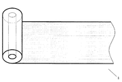
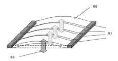
図1aと図1bは、本発明の実施形態になるスプール付き複合体1の連続ロールを示し、図1cは複合体1の一部の斜視図である。複合体の均整は、複合体1の異なる要素を図解する上で歪めてある。複合体1は、隆起面部分と陥凹面部分とからなるパターンを備える面3を有し、その面3の設計波形輪郭を形成する誘電体材料で出来ている薄膜2からなる。導電層4が面3に適用してあり、隆起面部分と陥凹面部分とからなるパターンに従って導電層が形成されるよう導電材料が堆積してある。有形日用品で言えば、薄膜2は一部形態において家庭用包装フィルムに類似するものである。それは、同様の厚さを有し、比較的曲げやすく柔らかいものである。しかしながら、それはこの種フィルムよりも弾性的であり、下記に説明することにする顕著な機械的異方性を有する。
1a and 1b show a continuous roll of a composite 1 with a spool according to an embodiment of the present invention, and FIG. 1c is a perspective view of a part of the
誘電体材料は、エラストマー或いは同様の特性を有する別の材料とすることができる。 The dielectric material can be an elastomer or another material having similar properties.
隆起面部分と陥凹面部分からなるパターンの故に、導電層4は薄膜2が延びる際に均一化され、矢印5が示す方向に沿って薄膜2が収縮する際に導電層4に対する損傷を引き起こすことなくその元々の形状を回復し、この方向がそれによって可撓性の方向を規定する。従って、複合体1は大きな歪に耐えることのできる可撓性構造の一部を形成するようにしてある。
Due to the pattern of the raised surface portion and the recessed surface portion, the
上記した如く、波形面輪郭は導電層を堆積する前に誘電体薄膜2内へ直に型押し或いは成形する。波形により高弾性係数からなる電極材料、例えば金属電極を用いた可撓性複合体の製造が可能になる。これは、導電層4を適用しつつ誘電体薄膜2へ予伸長或いは予歪の適用を迫られることなく得ることができ、完成した複合体1の波形輪郭は誘電体薄膜2の歪に依存はせず、また導電層4の弾性や他の特性に依存もしない。従って、波形輪郭は一貫した仕方で誘電体薄膜2の実質全面3に亙り複製され、この複製を制御することが可能になる。さらに、この手法は標準的な複製とリール間被覆を用いる可能性を提供し、それによってこの製法は大量生産に適したものとなる。例えば、導電層4は標準的な市販の物理的蒸着(PVD)技法を用いて誘電体薄膜2の面3に適用することができる。この手法の利点は、異方性が設計によって決まることであり、現実の異方性が誘電体薄膜2の面3に配設された波形輪郭と波形輪郭に従う導電層4の特性の結果として得られる。
As described above, the corrugated surface contour is stamped or molded directly into the dielectric
図1cに示す複合体1は、矢印5が規定する方向に誘電体薄膜2の可撓性の範囲内の可撓性と、矢印6が規定する方向に導電層4の剛性の範囲内の剛性とを有するよう設計してある。図1では可撓方向が複合体1の長さに沿うのに対し、図1bの可撓方向は複合体1を横切るものとなる。このことは図1a内の複合体1を横切る細線により図1bの複合体1沿いに示してあり、細線は波形輪郭を形成する隆起面部分と陥凹面部分からなるパターンを表している。複合体1は、極めて長い長さの図1aと図1bに示したスプールとして保存できるいわゆる「無端」複合体にて製造することができる。この種の半完成品は、変換器等、例えばアクチュエータの製造に使用することができる。
The composite 1 shown in FIG. 1c has a flexibility within the range of flexibility of the dielectric
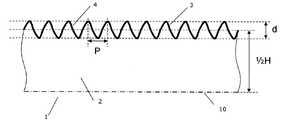
図2a〜図2fは、明瞭さに配慮して網掛けを省略した本発明の実施形態になる複合体1の断面図の一部を示す。各部の底部の対称線10が示す如く、各部は複合体1の半分を示すだけである。さらに、導電層4は誘電体薄膜2の下面に堆積させることができ、この下面は波形面もまた形成し、それによって電場応答複合体、すなわち誘電体薄膜により仕切られた少なくとも二つの導電層を形成することができる。さらに、各部は各複合体の長さ方向の小部分を示すだけである。図示目的に合わせ、図2a〜図2gの比は一定していない。図2gは、図2a,2b,2c,2d,2e,2fの拡大断面図である。図2a〜図2gに示した複合体1は、例えば図1aの複合体である。すなわち、複合体1は、隆起面部分と陥凹面部分とからなるパターンを持った面3を有する誘電体材料で出来た薄膜2を備え、それによって面3の波形輪郭を形成している。面3は、前記した指向的可撓性複合体を形成する導電層(図2gに示す)を備える。図2a〜図2fに示す如く、隆起面部分と陥凹面部分からなるパターンは様々な形状を持たせて設計することができる。
2a to 2f show a part of a cross-sectional view of the composite 1 according to an embodiment of the present invention in which shading is omitted for the sake of clarity. Each part only represents half of the composite 1 as indicated by the
波形輪郭は、一連の良好な周期的正弦波様の三次元微細構造により表すことができる。さもなくば、波形輪郭には三角輪郭や四角輪郭を持たせることができる。波形電極の機械的撓み係数Qは、波形の深さdと導電層4の厚さh(図2g参照)との間の寸法比と、波形の深さdとその周期Pとの間の寸法比とにより決まる。最も支配的な要因は、波形の高さdと導電層4の厚さhとの間の寸法比である。撓み係数が大きくなるほど、構造はより可撓性を有することになる。完全な可撓性を想定した場合、波形の深さdとその周期Pとの間の寸法比について、理論的には元の長さに比べ湾曲輪郭は約32%、三角輪郭は約28%、四角輪郭は約80%伸長させることもできる。しかしながら、実際にはこれは事実ではなく、何故なら四角輪郭は垂直梁と水平梁を備え、そのことが異なる可撓性をもたらし、何故なら垂直梁は屈曲し、それによって変位方向に極めて順応する動きが生まれ、一方で水平梁はずっと剛性があり、何故ならそれらは変位方向に延びるからである。それ故、湾曲輪郭を選択することがしばしば望ましい。
The waveform contour can be represented by a series of good periodic sinusoidal three-dimensional microstructures. Otherwise, the waveform contour can have a triangular contour or a square contour. The mechanical deflection coefficient Q of the corrugated electrode is determined by the dimension ratio between the corrugation depth d and the thickness h of the conductive layer 4 (see FIG. 2g), and the dimension between the corrugation depth d and its period P. It depends on the ratio. The most dominant factor is the dimensional ratio between the waveform height d and the thickness h of the
図2a〜図2fに示す複合体1では、誘電体薄膜2内に押し込み或いは成形した波形パターンは一連の良好に形成された周期的な正弦波状三次元微細構造により表すことができる。波形輪郭は、図2a〜図2fに示す如く薄膜2の上面3に形成してある。対称線10が示す如く、第2の波形輪郭が薄膜の下面(図示せず)に形成してある。図2a〜図2f中、断面は可撓性の方向に沿って走っている。可撓方向に垂直に平行な直線は隆起面部分と陥凹面部分の頂部と底部、すなわち正弦波状微細構造の波の山と谷を表す。これは、図1aと図1cにより明瞭に見て取れる。これらの平行な直線に沿って可撓性は極めて低く、すなわちあらゆる実用目的にとって複合体1はこの方向に可撓性がない。換言すれば、この設計は一次元的な波を表し、それが導電層の適用時に誘電体薄膜2を異方性可撓性を有する電場応答複合体1へ変形し、ここで薄膜は自由に収縮或いは伸長し、一方で垂直方向に配置された断面方向は導電層4の機械抵抗がもたらす内蔵境界条件のお陰で「凍結」される。
In the composite 1 shown in FIGS. 2a to 2f, the waveform pattern pressed or formed in the dielectric
図2a〜図2gにおいて、dは平均の或いは代表的な波形の深さ、すなわちこのパターンの隆起部分と隣接陥凹部分との間の平均の或いは代表的な距離を表す。Hは、誘電体薄膜2の平均厚さを表し、hは誘電体層4の平均厚さを表す。好適な実施形態では、誘電体薄膜2の平均厚さHは10μm〜100μmの範囲にある。図2a〜図2cは異なる波形の深さdを有する複合体1を示すものであるが、波形周期Pは図示の3個の複合体について実質同一である。図2dと図2eの複合体1を比較するに、波形深さdは実質同一であるが、図2eの複合体1の波形周期Pは図2dに示した複合体1の波形周期Pよりも大である。ここで比較するに、図2fの複合体1はより小さな波形深さdとより大きな波形周期Pとを有する。
2a-2g, d represents the average or typical corrugation depth, i.e., the average or typical distance between the raised portion of the pattern and the adjacent recess. H represents the average thickness of the dielectric
本発明に従い説明した導電層4の形をなす異方性波形可撓性金属電極を有する誘電体薄膜2の特性は、発明者が開発した設計規準に従う設計により最適化される。これらの設計規準は、誘電体材料および導電層の材料の誘電体特性と機械特性を考慮した。
The characteristics of the dielectric
一方で誘電体材料の相対的誘電率と破壊電界と、他方で電極間の電位差が、誘電体薄膜2の平均厚さHの範囲を決める設計パラメータとなる。誘電体材料の特徴的特性は、通常Wacker−Chemie社やDow Corning社等の誘電体製造業者等により提供されている。
On the other hand, the relative dielectric constant and breakdown electric field of the dielectric material, and on the other hand, the potential difference between the electrodes are design parameters that determine the range of the average thickness H of the dielectric
波形深さdは、電極間に位置する誘電体薄膜全体の比較的一様の電界分布を得るべく誘電体薄膜厚さHについて最適化する。この種最適化工程は、有限要素模擬法を用いて行われる。高d/H比は非一様電界分布に対応し、低d/H比は比較的一様な電界分布に対応する。 The waveform depth d is optimized with respect to the dielectric thin film thickness H in order to obtain a relatively uniform electric field distribution of the entire dielectric thin film positioned between the electrodes. This kind of optimization process is performed using a finite element simulation method. A high d / H ratio corresponds to a non-uniform electric field distribution, and a low d / H ratio corresponds to a relatively uniform electric field distribution.
異方性特性と可撓性特性は、一方で成形加工と他方で波形形状を取り込む導電層とにより誘電体薄膜、例えばエラストマー薄膜の面に与えられる形状と幾何構造の複合結果となる。電極層厚さhと波形周期Pは、「面内」方向に可撓性があって横断方向「面内」方向に殆ど可撓性のない金属電極を有する誘電体薄膜を得るべく、波形深さdについて最適化する。一方向に非常に可撓性のある薄膜は、電極に損傷する危険を伴うことなくこの方向に比較的低レベルの力を印加することでこの方向に大幅に引き伸ばす、すなわち伸長させることのできる薄膜であり、横断方向に力を印加したときに横断方向に非常に制限された伸長を有する薄膜である。電極の可撓性を最適化すべく、d/P比とh/d比を最適化しなければならない。高d/P比は頗る可撓性のある電極をもたらし、低d/P比は可撓性のより少ない電極をもたらす。高h/d比はより可撓性の少ない電極をもたらし、低d/P比は頗る可撓性のある電極をもたらす。波形電極付きの誘電体薄膜の異方性の程度は、複合体が撓む方向と複合体が殆ど撓まない横断方向との間の可撓性比により決まる。高い可撓性比は頗る異方性のある構造に帰結し、低い比は等方性に近い構造に帰結する。 The anisotropic and flexible properties are the combined result of the shape and geometric structure imparted to the surface of a dielectric thin film, such as an elastomer thin film, on the one hand by the molding process and on the other hand by the conductive layer that captures the corrugated shape. The electrode layer thickness h and the corrugation period P are determined by corrugation depth to obtain a dielectric thin film having a metal electrode that is flexible in the “in-plane” direction and hardly flexible in the transverse “in-plane” direction. Optimize for d. A film that is very flexible in one direction can be stretched or stretched significantly in this direction by applying a relatively low level of force in this direction without the risk of damaging the electrodes. A thin film having a very limited elongation in the transverse direction when a force is applied in the transverse direction. In order to optimize the flexibility of the electrodes, the d / P ratio and the h / d ratio must be optimized. A high d / P ratio results in a much more flexible electrode, and a low d / P ratio results in a less flexible electrode. A high h / d ratio results in a less flexible electrode, and a low d / P ratio results in a much more flexible electrode. The degree of anisotropy of the dielectric thin film with corrugated electrodes is determined by the flexibility ratio between the direction in which the composite is bent and the transverse direction in which the composite is hardly bent. A high flexibility ratio results in a more anisotropic structure, and a lower ratio results in a more isotropic structure.
設計パラメータ(H,d,h,P)に関する範囲が前記説明に従って一旦特定されると、可撓性の程度とそれが受けることのできる可撓性の方向の最大の伸長と駆動力の如何の点で、導電層の形態において金属電極付きの誘電体の性能を予測することが可能となる。横断方向の剛性もまた、予測することができる。これらのパラメータに関する精製工程は、必要に応じて行うことができる。 Once the range for the design parameters (H, d, h, P) has been specified according to the above description, what is the degree of flexibility and the maximum extension in the direction of flexibility it can receive and the driving force? In that respect, it is possible to predict the performance of a dielectric with a metal electrode in the form of a conductive layer. Transverse stiffness can also be predicted. The purification process regarding these parameters can be performed as necessary.
所与の駆動力について、本発明に従って製造、すなわちその上に電極を堆積した誘電体材料から作成したアクチュエータは、ずっと小さな重量を有し、すなわち相当の駆動力を供給することのできる磁気アクチュエータ等の従来のアクチュエータよりも少なくとも5分の1の小さな重量を有することに、留意されたい。このことは、アクチュエータの容積と重量が関連する場合の応用にとって非常に重要である。 For a given driving force, an actuator made from a dielectric material manufactured according to the present invention, i.e. having electrodes deposited thereon, has a much smaller weight, i.e. a magnetic actuator capable of supplying a considerable driving force, etc. Note that it has a weight that is at least one-fifth lower than conventional actuators. This is very important for applications where the volume and weight of the actuator are related.
全ての設計パラメータを一旦最適化すると、波形の幾何構造向けの厳密な仕様に従い金型を設計する。 Once all design parameters are optimized, the mold is designed according to strict specifications for the corrugated geometry.
有限要素法静電模擬に基づき、本発明の発明者は比d/Hを1/30〜1/2の範囲とすべきことが分かった。例えば、1/5の比と約4μmの波形深さを持たせることで、誘電体薄膜2の厚さはほぼ20μmとなる。さらに、波形深さdと波形周期Pとの間の比d/Pと導電層の厚さhと波形の深さdとの間の比h/dは、電極の可撓性に直接影響する重要な比となる。好適な実施形態では、比d/Pは1/50〜2の範囲とし、比h/dは1/1000〜1/50の範囲とする。
Based on the finite element method electrostatic simulation, the inventors of the present invention have found that the ratio d / H should be in the range of 1/30 to 1/2. For example, by giving a ratio of 1/5 and a waveform depth of about 4 μm, the thickness of the dielectric
誘電体薄膜2の平均厚さHを決めるときに検討する別の問題は、誘電体材料に関連するいわゆる破壊電界である。導電層4を誘電体薄膜2の各面に堆積し、それによって電場応答複合体を形成すると、所与の材料厚さHに対しこれらの導電層間の電圧V、すなわち材料の破壊電界V/Hを超えないようにすべく、誘電体薄膜2の厚さHに対応する距離に関する最大値が存在する。誘電体薄膜2が面積3全体に厚さの大きなばらつきを呈すると、導電層間の所与の電圧について電界と厚さのばらつきは同じ水準となろう。その結果、より高い局所電界を有する誘電体薄膜2の一部はより小さな局所電界を有するものよりも伸長しよう。さらに、複合体1が破壊電界近くで動作する変換器の状況にあっては、この種ばらつきが変換器を損傷することがある。何故なら誘電体薄膜2の一部が破壊電界を上回る電界にさらされることになるからである。従って、誘電体薄膜2を加工するときに最大に可能な範囲への平均厚さのばらつきを低減させることが非常に重要である。加工上の理由から、10%の平均厚さのばらつきは受容可能と考えられる。設計により、すなわち本発明に従って波形電極を有する変換器を製造するときに、これらの値は比較的正確な仕方で制御することができる。
Another problem to consider when determining the average thickness H of the dielectric
図3aと図3bは、ゼロ電位差にさらされ(図3a)、高電位差にさらされる(図3b)誘電体薄膜2により仕切られた二つの導電層4からなる電場応答複合体1を示す。図3bに示す如く、誘電体薄膜2を延ばし、その一方で電位差にさらしたときに、導電層4は均一化される。このことは、明瞭さに配慮し網掛けを省いて、経時的に異なる段階における電場応答複合体1の断面の一部を示す図4a〜図4cに詳しく図示してある。対称線10が、複合体1が各面に堆積された導電層4を有する電場応答複合体である各図の下部に示してある。図4aはゼロ電位差にさらされる電場応答複合体1を示すものであり、波形深さは設計深さdであり、波形周期は設計周期Pである。図4bには、誘電体薄膜2が可撓方向に延び、低減された厚さH’の薄膜が得られることが図解されている。さらに、導電層4はより小さな波形深さd’とより大きな波形周期P’をもたらすよう均一化してある。図4cは、時間経過した段階での電場応答複合体1を示し、薄膜2の厚さH”はさらにもっと低減してあり、波形深さd”はさらに小さくしてあり、波形周期P”はより大きくしてある。
FIGS. 3a and 3b show an electric field
本発明に従って生成されるコンデンサが「自己回復」機構を呈することに、留意されたい。自己回復機構は、極薄電極付きコンデンサの特性である。コンデンサからなる誘電体材料が含有物やピンホール等の欠陥を有するときに、それが行われる。所与の厚さを有するこの種コンデンサについては、電極間の印加電位差が前記に規定されたいわゆる破壊電圧に近づくと、平均電界は危険な破壊電界に近づく。しかしながら、欠陥を有する領域では、この危険な破壊電界を超え、欠陥箇所の誘電体薄膜厚さにかかる加速された衝突電荷のためにカスケード効果が発生し、それによって誘電体材料にかかる大きな突入過渡電流が誘起される。このことでマイクロ秒範囲或いはそれをずっと下回る特性時間でもって局所的過渡的過熱が生じる。それは欠陥箇所とそれらのごく近傍の極薄の対向電極の材料を「減少/消滅」させるに十分となる。これにより、電極材料がそれ以上存在しない欠陥を囲む領域が生まれる。さらに、減少した電極材料を有する領域の寸法は局部電界に合わせ増大する。しかしながら、この種コンデンサは破損せず、連続して動作する。かくして、「自己回復」と呼ばれる。減少領域が全体としてコンデンサの全面積のごく無視可能な一部を表す限り、このことはコンデンサの性能に対しごく僅かな影響力しか与えないことになる。自己回復はコンデンサが厚肉の電極で出来ている場合には生じないが、それは局所的な過熱レベルが欠陥箇所において厚肉電極材料を減少させるに十分でないからである。その場合、致命的な破壊に至ると、コンデンサに必然的な瞬時的破損が発生する。実際、本発明の発明者は最大0.2μmまでの厚さを有する金属電極を作成し、故障した状態においてコンデンサを動作させたときでさえ、自己回復を常に観察した。これはコンデンサに対するどんな実質的損傷も引き起こさず、コンデンサはそれ故に作動し続ける。 Note that capacitors produced in accordance with the present invention exhibit a “self-healing” mechanism. The self-healing mechanism is a characteristic of a capacitor with an ultrathin electrode. This is done when the dielectric material comprising the capacitor has defects such as inclusions and pinholes. For this type of capacitor with a given thickness, the average electric field approaches a dangerous breakdown electric field when the applied potential difference between the electrodes approaches the so-called breakdown voltage defined above. However, in areas with defects, this dangerous breakdown electric field is exceeded and a cascade effect occurs due to accelerated impact charges on the thickness of the dielectric thin film at the defect location, thereby causing large inrush transients on the dielectric material. A current is induced. This causes local transient overheating with microsecond range or characteristic time well below. It is sufficient to “reduce / disappear” the defects and the very thin counter electrode material in their immediate vicinity. This creates a region surrounding the defect where no more electrode material exists. Furthermore, the size of the region with reduced electrode material increases with the local electric field. However, this type of capacitor does not break and operates continuously. Thus, it is called “self-healing”. As long as the reduced area represents a negligible part of the total area of the capacitor as a whole, this will have a negligible impact on the performance of the capacitor. Self-healing does not occur when the capacitor is made of thick electrodes because the local overheating level is not sufficient to reduce the thick electrode material at the defect site. In that case, if the fatal destruction occurs, the capacitor is inevitably damaged instantaneously. In fact, the inventors of the present invention have made metal electrodes with a thickness up to 0.2 μm and have always observed self-healing even when the capacitor is operated in a faulty state. This will not cause any substantial damage to the capacitor and the capacitor will therefore continue to operate.
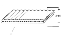
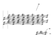
図5乃至図9は、それによって多層複合体を作成する複合体1の波形の例を示すものである。図5aと図6aに示す如く、電場応答多層複合体15,16はそれぞれの複合体1が前面20と背面21を有する誘電体薄膜2を備え、背面21が前面20に対向する少なくとも二つの複合体1を備える。前面20は隆起部分と陥凹部分からなる面パターン3と面部分3の少なくとも一部を被覆する第1の導電層(図示せず)とを備える。図5aと図6aは多層複合体15,16の一部だけを示すものであり、その部分は図解目的に合わせ別次元の均整を有する。
FIGS. 5 to 9 show examples of the waveform of the composite 1 thereby creating a multilayer composite. As shown in FIGS. 5 a and 6 a, the electric field
図5aと図5bは、その前面20を下記において一般に前面−背面間多層複合体15と呼ぶ隣接複合体1の背面21に対向する状態で配置した第1の複合体1を有する電場応答多層複合体15を示す。この種積層工程では、第1の複合体1の導電層は第2の複合体1の背面と直接当接する状態にある。複合体1は、誘電体薄膜2の生成に使用するのと同種のエラストマーの使用或いはさもなくば二つの複合体1を接着剤を使用しないで積層するかのいずれかで積層してある。一部目的に合わせ、多層複合体を接着剤を用いない積層複合体で作成することが好ましい。これらの場合、波の谷は単純に空気で充たされる。
5a and 5b show an electric field responsive multilayer composite having a
隆起面部分と陥凹面部分からなるパターン3のために、薄膜が延びる際に各複合体の導電層を均一化することができ、薄膜が矢印5(図5b参照)が規定する方向に沿って収縮する際に導電層に対し損傷を招くことなくその元々の形状を回復し、この方向がそれによって可撓方向を決める。すなわち、図5bに示した多層複合体15は矢印5の方向に頗る可撓性を有するよう設計してあり、矢印6の横方向に頗る剛性を有するよう設計してある。
Because of the
図5cと図5dは、ゼロ電位差にさらし、高電位差にさらす電場応答多層複合体15を示す。図5dから判るように、この誘電体薄膜を延び、その一方で電位差にさらしたときに導電層は均一化する。さらに、多層複合体を電位差にさらしたときに波の谷の深さ(波の深さd)を低減させることが理解できる。複合体は、高電位差を積層複合体へ印加することで結合でき、それによって一つの複合体の薄膜と隣接複合体の導電層は追加の接着剤を使用することなく互いに密着させることができる。かくして、それらは静電力により緊密に当接する状態に持ち込むことができる。さもなくば、エラストマーで作成したときに若干粘着性となる誘電体薄膜の特性のために、それらは例えばローラの使用によりそれらを互いに押圧することで相互に密着させることができる。
Figures 5c and 5d show the electric field
これまでの代替例として、図6aと図6bは、その背面21を下記において一般に背面−背面間多層複合体16と呼ぶ隣接複合体1の背面21に対向する状態で配置した第1の複合体1を有する電場応答多層複合体16を示す。複合体1は、複合体1の誘電体薄膜2に類似の特性を有するエラストマー接着剤の使用によっても密着結合させられる。さもなくば、二つの複合体1は接着剤の使用によらずに積層させる。
As an alternative so far, FIGS. 6a and 6b show a first composite with its
図6aに示した電場応答多層複合体16では、波形面3を複合体1を波形化する前或いは後に導電層でもって被覆することができる。背面−背面多層複合体16は、誘電体薄膜2内の欠陥や導電層内のピンホール等の影響を隣接層がごく近傍に同様の瑕疵が持たない場合により危険でないものにできる利点を有する。
In the electric field
個別複合体1は同一の生産工程において作成した場合、各複合体1の同一場所に同一の瑕疵が存在する増大した危険性が存在することになろう。この種瑕疵の影響を低減させる上で、一つの複合体1の位置を隣接複合体1に対しシフトさせ、或いは複合体1を相互に回動させることが好都合であろう。
If the
積層加工は、製造工程における不可欠の工程を表す。かくして、張力制御付きの精密な波形成形機を使用すべきである。 Lamination processing represents an indispensable process in the manufacturing process. Thus, a precise corrugating machine with tension control should be used.
多層複合体15と同様、図6bに示す複合体15と複合体16は矢印5の方向に頗る可撓性を持たせて設計し、矢印6の横断方向に頗る剛性を持たせて設計してある。
Similar to the
図6cと図6dは、ゼロ電位差へさらし、高電位差へさらす電場応答多層複合体16を示す。図6dから判るように、電位差にさらしたときに、誘電体薄膜は延び、その一方で導電層は均一化される。
Figures 6c and 6d show the electric field
図7aは、図5aに示した種の電場応答多層複合体15が具体的要請に応じて無制限の数の複合体1をさらに収容できることを示すものである。図5aの多層複合体は作動しない二つの誘電体薄膜2の中の一つの誘電体薄膜2を含み、すなわち二つの誘電体薄膜2の一方だけを二つの導電層(図示せず)間に配置してある。図7aは多数の複合体がこのような電場応答多層複合体15に対する非作動層の影響を低減させることを示すものであり、何故なら最低部の複合体15を除く全てが電極間に位置するからである。
FIG. 7a shows that an electric field
図7bは、数に制限のない複合体1を含む電場応答多層構造15を形成する代替法を示すものである。複合体1は、複合体1が互いに直接当接しないような仕方で複合体1間に配置した接着剤層22により積層してある。接着剤層22の材料は、伸長能力の点で複合体1の誘電体材料のそれと類似の特性を有する。これは、多層構造15が作動するときに誘電体材料と共に接着剤層22が伸長できるようにするためである。かくして、接着剤層22は都合よくはエラストマーから、すなわちエラストマー様特性を持った材料から作成することができる。
FIG. 7 b shows an alternative method of forming an electric field
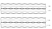
図8中、図6aにも示した同種の二つの電場応答多層複合体16、すなわち背面−背面複合体を互いの上に積層してある。この電場応答多層複合体では、導電層は互いに当接する2個一組をなす。二つの誘電体薄膜2が、二つの導電層からなるこの種組のうちの二つの間に配置してある。この積層体は、個別層において製造欠陥の低減された影響をもたらす。さらに、第3のもしくはよりさらなる一(又は複数)の電場応答多層複合体16を多層複合体に追加することができる。
In FIG. 8, two similar electric field
図9は、図8に示した積層体に類似の多層複合体16の積層体を示す。しかしながら、図9に示す状態では、背面−背面多層複合体16は2個一組で積層してあり、この2個一組で積層した多層複合体16をそこで併せ積層してある。図9に示す積層体では、互いに対向する2個一組の隣接積層体からなる導電層が同一の極性を有することが保証される。従って、この種積層体は電極を短絡させる危険性を伴うことなく巻回することができ、それ故に積層体は例えば管状変換器を形成する上で巻回に適したものとなる。
FIG. 9 shows a stack of
図10aは、巻回する図5aに示す前面−背面電場応答多層複合体15を示す。複合体1は非常に長い長さ、いわゆる「無端」の複合体で製造できるため、多層複合体15は非常に長い長さで製造し、それによって多数の巻回体からなる巻回多層複合体の製造を可能にすることができる。
FIG. 10a shows the front-back electric field
図10bは、ロッド23周りの多層複合体15の巻回を示すものである。ロッド23は多層複合体15の端部に配置してあり、複合体15はそこで図示の如くロッド23周りに巻回する。それによって、多層複合体15は巻回管形状が得られる。
FIG. 10 b shows the winding of the
図11aと図11bは、巻回し或いはさもなくば積層した変換器を形成するのに適した複合体24の一部を示す。複合体24は隆起面部分と陥凹面部分からなるパターンを持った面を有する誘電体材料で出来た薄膜2を備え、それにより設計された波形輪郭の面を形成し、すなわち薄膜2は図1cの複合体の薄膜2に類似する。この場合、薄膜2は交互介挿パターンにて配置した負電極部25と正電極部26を有する導電層を備え、すなわち負電極部25と正電極部26はその間の空隙に交互に出現する。空隙内では、導電層は誘電体薄膜上に堆積されていない。矢印27は、複合体24が図13aに示す非常に長い「無端」複合体や図13bに示す折り畳まれた複合体にできることを示している。
Figures 11a and 11b show a portion of a composite 24 suitable for forming a wound or otherwise stacked transducer. The composite 24 comprises a
図12a〜図12cは、図11の複合体24の一つの可能な作成方法を示す。図12aは、二つのロール30上の非常に長い薄膜である薄膜2を示す。導電層(図示せず)は、非連続蒸着ロール間法を用いて薄膜2上に堆積させる。矢印31は、加工方向を示す。導電層は、電極部25,26間に空隙を配設すべくシャドーマスク32を介して堆積する。導電層を薄膜2の一領域に堆積すると、薄膜2は矢印31の方向に巻かれ、停止する。シャッタ(図示せず)が開き、導電層が薄膜2の隣りの領域に堆積され、この領域は先の領域に隣接しており、同一の極性を持った電極間の連続する過渡的当接を保証する。このシャッタは、導電層の所要厚さが達成されたときに閉じる。電極がシャドーマスクを介して堆積されるという電極堆積原理は、実用上の理由から一定の幅と空隙を有する電極の製造により適したものである。代替例として、空隙はレーザ切除により作成することもできる。事実、レーザ切除により空隙を作成することは好ましく、何故ならこの種技法を用いると、各空隙とかくして導電層の各部分の可変幅との間に可変距離を持たすことが非常に簡単になるからである。このことを、下記により詳細に説明することにする。
12a-12c show one possible method of making the composite 24 of FIG. FIG. 12 a
図13aは、巻回複合体35として形成した図11aと図12a,12bの複合体24aを示す。DとRは、複合体24をその上に巻回するロール36の直径と半径を表す。実線は正電極を表し、対して点線は負電極を表す。明瞭さに配慮し、巻回複合体は同心円により図示してあることに留意されたい。しかしながら、実際には巻回複合体が螺旋パターンを形成していることは理解されたい。電極25,26の幅wとこれら電極部間の空隙(gap)の幅は、下記の如くロール36の断面積に基づき決定される。すなわち、2π(R)=w+gapであり、ここで空隙はwに比し非常に小さいものである。さらに、複合体24aの厚さtが空隙よりも小さいことが好ましい。さもなくば、この巻回加工により形成される変換器の効率は小さくなる。複合体24aを転動させることで巻回体を作成すると、空隙は先の巻回体に対し薄膜厚さの水準2πt・nで接線方向にシフトする。かくして、空隙シフトが空隙幅を超えた場合、同極性を有する電極は重複しがちとなり、これがコンデンサの対応部分を非作動とする。本方法は、限定された巻回数を有するアクチュエータを構築し、予歪構造すなわち電極部と空隙を平坦な管状アクチュエータの平坦部分に対応する誘電体ウェブの一部に堆積する平坦な管状アクチュエータにおいて動作させるのに好適である。可変幅ながら一定の空隙幅を有する電極の設計にレーザ切除を用いる場合の代替方法は、ロール状にした管状アクチュエータにとってより適切なものとなる。この場合、空隙と減少させた領域の幅はレーザスポット寸法を動かすことで決まり、アクチュエータの成長周縁の所与の巻回体に関連する所与の電極幅が幅と空隙を巻回体周縁に合致させるようにする。
FIG. 13a shows the composite 24a of FIGS. 11a and 12a, 12b formed as a
同様に、図13bは折り畳まれた複合体37としての図11bの複合体24bを示す。対向極性の電極25,26が直接当接しないよう保証されるよう複合体24bを慎重に折り畳むことは、図13bから明白である。
Similarly, FIG. 13 b shows the composite 24 b of FIG. 11 b as a folded
図14aと図14bは、複合体24の折り畳みによる図11に示す複合体の積層体を示す。さもなくば、複合体は図1aと図2に示す種とすることもできる。複合体1,24は長い構造にて製造し、それによって複合体1,24の長さと幅を決め、隆起面部分と陥凹面部分からなるパターンを有する面3を持たせる。こパターンが共通方向に延びる波の山と谷を形成しており、共通方向は長尺構造の幅に実質沿って配置される。従って、複合体1,24は共通方向に垂直な方向、すなわち長尺構造の長さ沿いに可撓性を有する。
FIGS. 14 a and 14 b show a laminate of the composite shown in FIG. 11 by folding the composite 24. Otherwise, the complex can be the seed shown in FIGS. 1a and 2. The
図14aの複合体1,24は、長さに沿って長尺構造を折り畳むことで、すなわち得られる電場応答多層複合体40の幅が複合体1の幅に同一となるよう積層してある。複合体1,24の可撓方向の向きのために、電場応答多層複合体40は矢印41で示す方向に可撓性を有することになる。
The
図14bは、本発明の別の実施形態になる複合体1,24の積層体を示す。これは、図14aに示す実施形態に極めて類似するものである。しかしながら、この場合共通方向は長尺構造の長さに実質沿って配置され、複合体1,24はそれ故に図1bの複合体として長尺構造の幅に沿う方向に可撓性を有する。従って、得られる電場応答積層体42は矢印43で示す方向に撓むことになる。
FIG. 14 b shows a laminate of
かくして、図14aに示す積層複合体は積層複合体の長さ沿いに撓む。これは、図14aの構造が任意の長さ、すなわち任意の所望のストローク長にすることができることを意味する。同様に、図14bの積層複合体は積層複合体の幅に沿って撓む。このことは、図14bの構造が任意の幅で作成できることを意味する。かくして、意図した応用例の幾何学的要件に従い任意の適切な寸法をもって変換器を設計することが可能となる。 Thus, the laminated composite shown in FIG. 14a bends along the length of the laminated composite. This means that the structure of FIG. 14a can be of any length, ie any desired stroke length. Similarly, the laminated composite of FIG. 14b bends along the width of the laminated composite. This means that the structure of FIG. 14b can be created with an arbitrary width. Thus, it is possible to design a transducer with any suitable dimensions according to the geometric requirements of the intended application.
図15a〜図15cは、本発明の一実施形態になる直動(direct actuating)変換器50の斜視図である。図15a〜15cの直動変換器50は多層複合体、例えば図1a或いは図5に示した種を巻回させることで製造してある。図15aの変換器50aは中実であるのに対し、図15bの変換器50bは中空である。変換器50は任意の伸長形状、例えば実質的に円形や楕円形の或いは図15cに示す如く形成した湾曲する断面を有する実質筒状体形状を持たせることができる。
15a-15c are perspective views of a
図15a〜図15cでは、柱体状の変換器50を形成するよう巻回した複合体は矢印51で示す方向に平行な可撓方向を有する。従って、電気エネルギを直動変換器50の電極へ印加したときに、変換器50は矢印51の方向に軸方向に伸長する。変換器50を本発明の所定形態に従って適切に作成し寸法を持たせた場合、それらは軸方向伸長に抗しがちな軸方向負荷に対し相当の力を作用させることができる。
In FIGS. 15 a-15 c, the composite wound to form the
本明細書に先に示したように、本発明の電場応答複合体は極めて柔軟で曲げやすく、その曲げやすさにおいて通常の家庭用粘着フィルムやポリエチレン買い物バッグ用シート材料に類似する。複合体は、先に説明した如く、一つの方向に頗る伸長性があり、垂直方向には伸長性が極めて乏しいそのより高い弾性ならびにその機械的異方性によりそれらの材料とは異なる。 As previously indicated herein, the electric field responsive composites of the present invention are extremely flexible and easy to bend, similar to ordinary household adhesive films and polyethylene shopping bag sheet materials in their ease of bending. As explained above, composites are extensible in one direction and differ from these materials due to their higher elasticity, which is very poor in extensibility in the vertical direction, as well as their mechanical anisotropy.
発明者は、ここで複合体の柔軟性や可撓性や弾性にも拘らず、十分な長さの複合体を巻き上げることで形成したロールは非常に剛性のあるものとなろうことを了解している。薄膜の機械的異方性についてロールを適切に巻回した場合、機械的異方性が持ち込む軸方向可撓性を有することになり、また依然としてそれは軸方向負荷の下で曲げに十分に抗することができる。 The inventor understands that a roll formed by winding up a sufficiently long composite would be very rigid, regardless of the flexibility, flexibility and elasticity of the composite. ing. If the roll is wound properly for the mechanical anisotropy of the thin film, it will have the axial flexibility that mechanical anisotropy introduces, and it still resists bending under axial loading. be able to.
従って、導電電極層を有する波形異方性誘電体薄膜層の複合体は、管状要素の生成構造を、曲げを防止すべく十分堅牢にする上で十分な巻回数をもって管状形状へ巻回することができる。本文脈では、用語「曲げ」は印加された軸方向負荷のために屈曲することで伸長構造が変形する状態を意味する。伸長構造内部の何らかの剛性強化ロッド或いはばね等の追加の構成要素は、軸方向負荷の技術的な有用レベルの下で曲げを排除する上で十分な剛性を取得する必要の全くないことが分かっている。要求剛性は、単に複合材料からなる十分な数の巻回体を巻き上げることで得られる。 Therefore, the composite of the wavy anisotropic dielectric thin film layer having the conductive electrode layer is wound into a tubular shape with a sufficient number of turns to make the tubular element generation structure sufficiently robust to prevent bending. Can do. In this context, the term “bending” means a state in which the elongate structure deforms by bending due to an applied axial load. It has been found that any additional components, such as any stiffening rods or springs within the elongate structure, do not need to obtain sufficient stiffness to eliminate bending under the technically useful level of axial loading. Yes. The required rigidity can be obtained simply by winding up a sufficient number of wound bodies made of a composite material.
図15a〜15cに示した巻回構造は、剛性が曲げを排除するに十分な負荷の具体的な最大負荷レベルに耐えるよう設計してある。この具体的な最大レベルは、例えば所定レベルの伸長での所定レベルの力とすることができ、或いはそれを最大レベルの駆動力や遮断力或いは変換器を矢印51の方向に対しより短い長さへ圧縮したときに発生するより高い力レベルとすることもできる。 The winding structure shown in FIGS. 15a-15c is designed to withstand a specific maximum load level with a load sufficient to eliminate bending. This specific maximum level can be, for example, a predetermined level of force with a predetermined level of extension, or it can be the maximum level of driving force, shut-off force or transducer with a shorter length in the direction of arrow 51. It is also possible to achieve a higher force level that occurs when compressed into
本出願に記載した直動変換器用の設計パラメータは、発明者が開発した設計規準に従い最適化する。これらの設計規準により、アクチュエータ性能仕様に基づく巻回アクチュエータ(変換器)の最適寸法の決定が可能になる。 The design parameters for the linear motion transducer described in this application are optimized according to the design criteria developed by the inventors. These design criteria make it possible to determine the optimum dimensions of a wound actuator (transducer) based on actuator performance specifications.
電場応答複合体の機械的特性と静電特性は、単位面積当りの駆動アクチュエータ力とストロークを推定する根拠として使用する。本発明に従って記載された巻回アクチュエータは、例えば1μm範囲に厚さを有する図1aと図1bに示した極薄の電場応答複合体を巻回/スプール巻装することで作成する。この種の典型的なアクチュエータは数千の巻回体で作成でき、アクチュエータ壁厚の1mm当り100巻回ほどを含ませることができる。 The mechanical and electrostatic properties of the electric field response composite are used as a basis for estimating the drive actuator force and stroke per unit area. The winding actuator described in accordance with the present invention is made by winding / spooling the ultra-thin electric field response composite shown in FIGS. 1a and 1b, for example, having a thickness in the 1 μm range. A typical actuator of this kind can be made up of thousands of windings and can include as many as 100 turns per mm of actuator wall thickness.
駆動時に、直動/押動アクチュエータは電気エネルギを機械エネルギへ変換する。このエネルギの一部はアクチュエータ材料の潜在エネルギの形にして保存され、アクチュエータを放電させたときの使用に向け再度利用できるようになる。機械エネルギの残りの部分は、駆動用に効果的に利用可能となる。駆動エネルギへの機械的エネルギのこの残りの部分の完全な変換は、アクチュエータ構造が軸方向の圧縮のために公知の欠陥屈曲モードのように機械的に不安定とならない場合にのみ可能とされる。このことは、アクチュエータ長に関連してアクチュエータの断面積に適切に寸法を持たせることで達成できる。数学的には、これはオイラーの柱体安定性定理に対応するものである。本発明によれば、この定理は電場応答多層複合体の十分な巻数まで巻き上げることで形成される柱体アクチュエータにも当てはまる。 When driven, linear / push actuators convert electrical energy into mechanical energy. A portion of this energy is stored in the form of potential energy of the actuator material and can be reused for use when the actuator is discharged. The remaining part of the mechanical energy is effectively available for driving. Full conversion of this remaining portion of mechanical energy to drive energy is only possible if the actuator structure does not become mechanically unstable due to axial compression as in known defect bending modes. . This can be achieved by appropriately dimensioning the cross-sectional area of the actuator in relation to the actuator length. Mathematically, this corresponds to Euler's column stability theorem. According to the present invention, this theorem also applies to columnar actuators formed by winding up a sufficient number of turns of the electric field responsive multilayer composite.
最適化工程は、所与の適用に必要な力のレベルを規定することで始まる。次に単位面積当りの駆動力に基づき、そのレベルの力に至るのに必要な断面積を推定することが可能である。 The optimization process begins by defining the level of force required for a given application. Next, based on the driving force per unit area, it is possible to estimate the cross-sectional area required to reach that level of force.
筒状構造については、筒状体の長さと半径の間の所与の比に対する限界軸方向負荷すなわち力Fcは、
Fc=c・π2・E・A/(L/R)2
により与えられる。ここで、
cは境界条件依存定数、
Eは弾性係数、
Aは筒状体の断面積、
Lは筒状体の長さ、
Rは筒状体の半径である。
For cylindrical structures, the critical axial load or force Fc for a given ratio between the length and radius of the cylinder is
Fc = c · π 2 · E · A / (L / R) 2
Given by. here,
c is a boundary condition dependent constant,
E is the elastic modulus,
A is the cross-sectional area of the cylindrical body,
L is the length of the cylindrical body,
R is the radius of the cylindrical body.
ここで、その電極に電圧Vを印加することで駆動する筒形電場応答ポリマー変換器を考察する。非負荷状態では、変換器は単に細長いだけである。軸方向負荷が抑制されている場合、変換器は電圧Vと共に増大する負荷に対し力を作用させることになる。変換器を駆動させることのできる最大力Fmaxは、変換器の構成に依存する。 Now consider a cylindrical electric field responsive polymer converter driven by applying a voltage V to the electrode. In an unloaded condition, the transducer is simply elongated. When the axial load is suppressed, the transducer will exert a force on the load that increases with the voltage V. The maximum force F max that can drive the transducer depends on the configuration of the transducer.
所与の長さLと断面Aについて、このことはFmax<Fcよりも大きな力を許容しない仕方でもって電圧を制御する必要があることを意味する。所与の断面について、このことは筒状体の長さを限界の長さLc、すなわちL<Lcよりも小さくしなければならないことを意味し、Lcは下記の如く定義される。 For a given length L and cross-section A, this means that the voltage needs to be controlled in a way that does not allow forces greater than F max <F c . For a given cross section, this means that the length of the cylinder must be less than the critical length L c , ie L <L c , where L c is defined as:
所与の断面積と選ばれた最大力レベルを有する変換器50について、最大電圧レベルに関連する最大力レベル、すなわち限界の長さLcは公式
Lc≦{c・r2・π2・E/(Fmax/A)}1/2
から導出することができ、設計規範は、L<Lcとなる。
For a
The design rule is L <L c .
選択された電圧レベルでは、所要の断面を有する変換器50は所与の最大力、いわゆる0%伸長時の遮断力Fblをもって駆動することができる。この状況では、設計規範は、
Lc={c・r2・π2・E/(Fbl/A)}1/2
となる。
At a selected voltage level, the
L c = {c · r 2 · π 2 · E / (F bl / A)} 1/2
It becomes.
E=1MPa、Fbl/A=20N/cm2、c=2を有するエラストマーで出来た変換器50についてこれらの設計規範を適用するに、Fmax=Fblの設計規準はLbl=10・r、すなわちいわゆる細長比λは、遮断力に等しい負荷において非屈曲構造を得る上で下記の条件を満たさねばならない。
λ≦L/r=10
To apply these design criteria for a
λ ≦ L / r = 10
同じ変換器50に対する駆動力に関する、すなわち同じ半径rを有する筒状の対称的変換器50について代替的に選択されたより低いレベルでは、長さLに関する設計規範は下記の式
L≦Lbl・(Fbl/F)1/2
から導出することができる。
At a lower level with respect to the driving force for the
Can be derived from
これは、例えば10%伸長の駆動レベルが(1/4)・Fblの場合、そのときは10%伸長時の変換器の長さLが、
L≦Lbl・{1/(1/4)}1/2=Lbl・2
となることを意味する。
For example, if the drive level of 10% extension is (1/4) · F bl , then the length L of the converter at 10% extension is
L ≦ L bl · {1 / (1/4)} 1/2 = L bl · 2
Means that
オイラーの定理は、変換器ストロークに対する具体的必要性をもって変換器50と誘電体薄膜の選択された百分率の伸長の設計に適用することができる。増大した数の巻回数のお陰で筒状の対称変換器50a,50bの断面積Aの増大に対する制約は一切存在せず、オイラーの定理から導出された設計規準が実現されるのために、単純に所要レベルの駆動力を得るのに必要な巻回数を決めることが可能になる。従って、上記に記載された技術により所与の力レベルと直動用の所与のストロークにて非屈曲特性を有する誘電体変換器を構築することが可能となる。
Euler's theorem can be applied to the design of selected percentage stretches of
直動型容量性変換器の設計時に、曲げに対抗してその機械構造を寸法決めする必要がある。これは通常、Iとして知られるその断面二次モーメントを増大させることで果たされる。一例として、所与の厚さ(h)と幅(w)と長さ(L)を有する一片の紙面はその長さに平行な方向に紙面に僅かな力が印加されたときに屈曲することになる。しかしながら、それを幅方向に巻回させることで、それを曲げるのに非常に大きな力が必要となろう。巻回−平坦屈曲剛性比は、そこで(3/2)・{1+[w/(h/π)]2}により与えられる。この種の一例は、w=40mm、h=1mmとすることで、そこで比は約245となる。 When designing a direct acting capacitive transducer, it is necessary to dimension its mechanical structure against bending. This is usually accomplished by increasing its cross-sectional second moment, known as I. As an example, a piece of paper having a given thickness (h), width (w), and length (L) bends when a slight force is applied to the paper in a direction parallel to the length. become. However, by winding it in the width direction, a very large force will be required to bend it. The winding-flat flexural rigidity ratio is then given by (3/2) · {1+ [w / (h / π)] 2 }. An example of this type is w = 40 mm and h = 1 mm, where the ratio is about 245.
何らかの機械的不安定さに対抗するアクチュエータの安定化には、断面二次モーメントIを増大させることでその断面を寸法決めする必要がある。低い値のIはより安定性の乏しい構造に帰結し、高い値のIは曲げに対し非常に安定した構造に帰結する。構造を寸法決めする設計パラメータは、断面積Aに関する旋回半径rgと断面モーメントIである。低い値のrgはより安定性の乏しいアクチュエータに帰結し、高い値のrgは非常に安定したアクチュエータに帰結する。面積Aと旋回半径rgの両方について最適範囲を決めると、rgに関する巻回アクチュエータ壁厚についての最適範囲をt/rgの形で決めることが可能になる。面積Aと半径rgと壁の厚さtは、最大安定性に向けアクチュエータ断面を寸法決めする設計パラメータとなる。低い値のt/rgは極めて安定したアクチュエータ構造に帰結し、高い値のt/rgはより安定性のないアクチュエータ構造に帰結する。 Stabilization of the actuator against any mechanical instability requires that the cross section be dimensioned by increasing the cross section secondary moment I. A low value of I results in a less stable structure and a high value of I results in a very stable structure against bending. Design parameters for dimensioning the structure is the turning radius r g and a cross-sectional moment I about the cross-sectional area A. R g Low values of result in more stable poorly actuator, r g of high value results in very stable actuator. After having defined optimum ranges for both area A and radius of gyration r g, it is possible to determine the optimum range for the rolled actuator wall thickness about r g in the form of t / r g. The thickness t of the area A and radius r g and the wall is a design parameter for dimensioning the actuator cross-section toward the maximum stability. T / r g of low values result in very stable actuator structures, t / r g of high value results in a more stable without the actuator structure.
断面パラメータの範囲が一旦決まると、所要レベルの力に対し軸方向の圧縮による曲げが発生しないアクチュエータの最大長さを推定する必要がある。旋回半径rgの半径に対する長さLの比として規定される細長比が、オイラーの定理に関するパラメータとして一般に用いられる。低い値のL/rgは極めて安定したアクチュエータ構造に帰結し、高い値のL/rgは曲げに対しより安定しないアクチュエータ構造に帰結する。 Once the range of cross-sectional parameters is determined, it is necessary to estimate the maximum length of the actuator that does not cause bending due to axial compression for the required level of force. Slenderness defined as the ratio of the length L to the radius of the turning radius r g are generally used parameter in relation with Euler's theory. Low value of L / r g result in very stable actuator structures, the L / r g high values result in less stable actuator structures against bending.
最適能動直動アクチュエータに関する全ての設計パラメータが一旦決まると、μm範囲の特定の厚さを有する所与の電場応答複合体についてのアクチュエータ壁厚tと1mm当りの巻数nとに基づき、アクチュエータを構築するのに必要な総巻数を推定することが可能になる。 Once all the design parameters for the optimal active linear actuator have been determined, the actuator is constructed based on the actuator wall thickness t and the number of turns n per mm for a given electric field response complex with a specific thickness in the μm range It is possible to estimate the total number of turns required to do this.
好適な実施形態では、変換器の巻数nと壁厚tとの間の比n/tは、10巻回数/mm〜50巻回数/mmの範囲とすべきである。さらに、変換器の長さLと変換器の旋回半径rgとの間の比である細長比は20未満とすべきである。旋回半径rgは、Iを断面の面積モーメントとし、Aを変換器の断面積とすると、rg=(I/A)1/2となる。 In a preferred embodiment, the ratio n / t between the number of turns n of the transducer and the wall thickness t should be in the range of 10 turns / mm to 50 turns / mm. Furthermore, slenderness ratio is the ratio between the turning radius r g of the transducer and the length L of the transducer should be less than 20. The turning radius r g is r g = (I / A) 1/2 where I is the sectional area moment and A is the sectional area of the transducer.
かくして、本発明に従って変換器を慎重に設計することで、たとえ非常に柔らかな誘電体材料を使用したとしても、大きな駆動力を得ることが可能になる。駆動力は、より硬い材料から作られた従来の変換器、例えば磁気変換器に比肩するレベルに到達しさえする。このことは、大きな利点である。 Thus, careful design of the transducer in accordance with the present invention makes it possible to obtain a large driving force even if very soft dielectric materials are used. The driving force can even reach levels comparable to conventional transducers made from harder materials, such as magnetic transducers. This is a great advantage.
図16aは、本発明の一実施形態になる直動変換器におけるストロークの関数としての力を示すグラフである。変換器の異方可撓性導電層に電圧を印加すると、薄膜厚さ全体にかかる電界誘導圧縮は変換器の可撓方向に沿う伸長/ストロークへ変換される。圧縮歪はマクスウェル歪Pと呼ばれ、対応駆動力は静電力Felectrostaticと呼ばれる。伸長時に、誘電体材料は図16aに示す如く変換器ストロークと共に増大する対向力Felastomerを及ぼす。 FIG. 16a is a graph showing force as a function of stroke in a linear motion transducer in accordance with one embodiment of the present invention. When a voltage is applied to the anisotropic flexible conductive layer of the transducer, the field induced compression across the entire film thickness is converted into an extension / stroke along the transducer's flexible direction. The compressive strain is called Maxwell strain P, and the corresponding driving force is called electrostatic force F electrostatic . When stretched, the dielectric material exerts an opposing force F elastomer that increases with the transducer stroke as shown in FIG. 16a.
その結果、直動に利用可能な実効的力Factは記述した二つの力から導かれ、図16bに示す如くFact=Felectrostatic−Felastomerとなる。直動アクチュエータの力対ストロークを表す特性曲線は力変換器にとって一般的であり、ここでは駆動力は増大するストロークの関数として減少し、最後に図16bに表したようにストロークの最大値が「ゼロ」駆動力に対応するものに達する。 As a result, the effective force Fact that can be used for linear motion is derived from the two described forces, and F act = F electrostatic −F elastomer as shown in FIG. 16b. A characteristic curve representing the force vs. stroke of a linear actuator is common for force transducers, where the driving force decreases as a function of increasing stroke, and finally the maximum value of the stroke is “as shown in FIG. The one corresponding to "zero" driving force is reached.
図16cは、直動容量性変換器、すなわち巻回型変換器の異なる外径ごとに変換器ストロークの関数としての算出直動力の範囲を示すものである。数百乃至数千ニュートンの範囲の大きな駆動力を、発生させることができる。遮断力は、10%変換器ストロークにて規定される公称駆動力よりも通常4桁は大きなものとなる。0.5〜1MPaの範囲の弾性係数を備える40μmの厚さの誘電体材料で出来た直動容量性変換器は、一般的な駆動電圧3000ボルトについて単位面積当り0.1〜0.2N/mm2の範囲の力を発生することになる。大型変換器の断面を考えたときに、これは図16cに示す大きな駆動力に相応するものとなる。 FIG. 16c shows the range of calculated linear power as a function of transducer stroke for different outer diameters of a linear capacitive transducer, ie a wound transducer. Large driving forces in the range of hundreds to thousands of newtons can be generated. The breaking force is usually four orders of magnitude greater than the nominal driving force defined by the 10% transducer stroke. A direct acting capacitive transducer made of a dielectric material having a thickness of 40 μm with an elastic modulus in the range of 0.5-1 MPa is 0.1-0.2 N / per unit area for a typical drive voltage of 3000 volts. A force in the range of mm 2 will be generated. When considering the cross section of the large transducer, this corresponds to the large driving force shown in FIG. 16c.
図17aと図17bは、本発明の代替実施形態になる直動変換器52の斜視図である。図17aと図17bの変換器52は、筒状体の接線に沿う撓み方向を有する。従って、変換器52の伸長は矢印53が示す管状構造の周縁で発生し、すなわち変換器52は半径方向に伸長と収縮をさせられる。 17a and 17b are perspective views of a linear motion transducer 52 according to an alternative embodiment of the present invention. The transducer 52 of FIGS. 17a and 17b has a deflection direction along the tangent of the cylindrical body. Accordingly, the extension of the transducer 52 occurs at the periphery of the tubular structure indicated by the arrow 53, i.e., the transducer 52 is caused to expand and contract in the radial direction.
図18aは、平坦な管状構造60を形成する複合体1の積層体を示す。複合体1は、都合よくは図1aと図2に示す種とすることができる。変換器60は変換器の剛性を保証すべく十分に多数の密着結合複合体の積層体からなり、その剛性は予歪を与えることなく変換器が作動できるようにするに十分なものとしてある。変換器60は、例えば非常に平坦な管状構造にて図1aと図2に示す種の連続複合体を巻回することで製造してある。この設計を用いることで、前記した層の数に関する制約は取り除かれる。それによって、変換器60は図15a〜図15cを参照して前記したもの同様、必要なだけ強力に作成することができる。
FIG. 18 a shows a stack of
図18aに示した平坦な管状構造の変換器60は、二つの離間するロッド61の周りに複合体1を転動させて複合体1の巻回パターンを形成することで得られる。複合体1の可撓方向の向きのために、平坦な管状構造60は矢印62が示す方向に可撓性を有することになる。図18bは、二つのばね63により予歪を持たせた図18aの変換器を示す。
The flat
図19a〜図19cは、平坦な構造を有する変換器70の斜視図である。変換器70は変換器の剛性を保証すべく十分多くの密着結合複合体からなる多層複合体であり、その剛性は予歪を与えずとも変換器がアクチュエータとして作動できるようにするに十分なものとしてある。変換器70は、例えば図1aと図2に示した種の連続する複合体を平坦な構造にて積層することで製造する。この設計を用いることで、前記した所定数の層に関する制約は取り除かれる。それによって、変換器70は図15a〜図15cを参照して前記したものと同様、必要に応じただけ強力に作成することができる。変換器70aは変換器の剛性を保証する十分多くの密着結合複合体からなる多層複合体であり、その剛性は予歪を与えずとも変換器がアクチュエータとして作動できることを保証するに十分である。変換器70bは、幾つかの変換器70aを積層することで所定寸法としてある。これに対する代替例として、変換器70cはばね71により或いは他の弾性的に変形可能な要素により予歪を与えることもできる。
19a to 19c are perspective views of the transducer 70 having a flat structure. Transducer 70 is a multi-layer composite composed of enough tightly bonded composites to ensure the rigidity of the transducer, which is sufficient to allow the transducer to operate as an actuator without pre-straining. It is as. The transducer 70 is manufactured, for example, by laminating a continuous composite of the type shown in FIGS. 1a and 2 in a flat structure. By using this design, the constraints on the predetermined number of layers described above are removed. Thereby, the transducer 70 can be made as powerful as required, similar to that described above with reference to FIGS. 15a-15c.
変換器70aと70bには、応用例において変換器を取り付けるべく、例えば変換器をアクチュエータとして作動させるべく、固定フランジ72が配設してある。矢印73は、撓み方向を示す。
The
図20a〜図20eは、予荷重を付与した駆動中の変換器80を示している。図20aは、固定フランジ81を配設した平坦な変換器80の斜視図である。図20aの平坦な変換器80は、ばね82により予歪付与してある。従って、平坦な変換器80は矢印83が示す駆動方向を有する。図20bは、ばねを類似の第2の平坦な変換器80により置き換えた類似の平坦な変換器80を示す。図20cは変換器の半分を示すものであり、この変換器は図20bの変換器に類似しており、同一の変換器の所定数(その半分だけを図示)使用により寸法決めする。図20dと図20eは二つの代替変換器84,85を示すものであり、そのそれぞれは図18bの変換器に類似の隣接変換器により予歪を与える一定数の平坦な変換器80を備える。変換器84,85は、カーペット様構造内の図20dと壁様構造内の図20eにおいて交差方向に駆動する。
20a to 20e show the
図18〜図20の変換器は、一方向、すなわち可撓方向に予歪を必要とするだけであることに留意されたい。かくして、可撓方向を横断する方向の予歪は先行技術変換器には必要であるが、本発明になる変換器には必要ない。 Note that the transducers of FIGS. 18-20 only require pre-strain in one direction, the flexible direction. Thus, pre-straining in the direction transverse to the flex direction is necessary for prior art transducers, but not for transducers according to the present invention.
図21は、平坦な管状構造を有する二つの予歪付き変換器90を示すものであり、変換器90は長手方向に作動し、それによって駆動軸91を回動させる。
FIG. 21 shows two
図21bは、摺動目的に合わせガイド要素により支持される機械的接続体94を備える二つの機械的予歪付きの平坦な変換器92,93を示す。変換器92,93は、三つの状態にて図示してある。第1の状態では、変換器92,93は共に作動していない。しかしながら、それらには共に機械的に予歪を付与してある。第2の状態では、変換器93は作動している。変換器92は非作動状態にあるため、変換器93が変換器92を弛緩させ、それによって変換器92の機械的予歪の一部は解放される。第3の状態では、変換器92は作動しているが、変換器93は非作動である。変換器92はそれによって変換器93を弛緩させ、それによって変換器93の機械的予歪の一部を解放する。かくして、変換器92,93は機械的接続体94と組み合わさって二重能動変換器を形成し、ここでは変換器の一方が他方の変換器を弛緩させて機械的予歪を解放する。
FIG. 21b shows two mechanical pre-strained
図22は、第1の面100とこの第1の面100に対向する第2の面101とを備える誘電体薄膜2を備える電場応答複合体を示す。誘電体薄膜2の両面は、導電層でもって一部被覆してある。導電層の形状と位置のために作動部Aが存在し、ここでは導電層の電極部102,103が誘電体薄膜2の両面100,101を被覆している。導電層はさらに、誘電体薄膜2の第2の面101だけを一方の導電層の接点部104により被覆した第1の受動部Bと、電源誘電体薄膜2の第1の面100だけを他方の導電層の接点部105により被覆した第2の受動部Cとを形成している。その外観の如く、電場応答複合体は電源に電気的に接続するか、或いは導体を接点部104,105を結合することで複合体の駆動を制御する制御手段に接続することができる。たとえ図示した複合体が積層したり巻回したり折り畳んで多数の層を有する変換器を形成していたとしても、電極部102,103は例えば各接点部104,105内の層に導電性のワイヤやロッドを貫通させ、ワイヤやロッドを電源へ接続することで簡単に電源へ接続することができる。誘電体薄膜2の厚さと導電層の厚さとの間の比は、単に例示目的に過ぎない。図22に示す加工法は「オフセット」と呼ぶことができるが、それは相互に「オフセット」させた誘電体薄膜2の面100,101上に電極部102,103を適用することで接点部104,105を配設するからである。
FIG. 22 shows an electric field responsive composite comprising a dielectric
図23a〜23cは変換器を形成する多層複合体の二つの複合体1を空間シフトさせる三つの異なる方法を示すものであり、ここで各複合体1は誘電体薄膜上に導電層を備える。図示した複合体1は、変換器を駆動したときに延び或いは収縮する可撓方向を有する。図23aでは、接点部は図23bの可撓方向に沿ってシフトさせた空間となり、接点部は可撓方向に垂直にシフトさせてあり、図23cでは、接点部は可撓方向とこの可撓方向に垂直な方向の両方にシフトさせた空間となる。いずれの構造においても、多層複合体と何らかの歪の元すなわち可動部から離間する接続ワイヤやロッドや同様の導体との間に物理的接点が作成される領域を維持することが望ましい。図23dは、側面から見た多層複合体を示す。
FIGS. 23a-23c show three different ways of spatially shifting two
かくして、図22と図23a〜23cは接点部104,105を配設する二つの異なる原理、すなわち図22の「オフセット」原理と図23a〜23cの「空間シフト」原理とを示す。これらの原理は様々な積層法と組み合わせることができ、意図する応用例にとって適切な原理をしかるべく選択することができる。
Thus, FIGS. 22 and 23a-23c illustrate two different principles of disposing the
図24は、接点部104,105が導電層の一部を形成し、電極部102,103の一側に延長孤立部を形成することを示すものである。多層複合体内の二つの隣接する複合体の孤立部を異なる配置としてあり、これにより隣接複合体の接点部104,105は互いに距離を置くことになる。
FIG. 24 shows that the
図25は、それぞれ導電層を備える二つの複合体を示す。複合体を多層複合体に合体させると、それらは互いにオフセットし、これにより各複合体上の導電層の一部が他方の複合体上の対応接点部105から離れた接点部104を形成する。
FIG. 25 shows two composites each comprising a conductive layer. When the composites are combined into a multilayer composite, they are offset from each other, thereby forming a
図26と図27は、同様に図15aと図15bに示した管状変換器50を示す。管状変換器は、指示した接点部104,105にて電源へ接続してある。
FIGS. 26 and 27 similarly show the
図28は、平坦な管状構造を有する変換器110を示す。変換器は、内面に接点部104,105を備える。接点部は、例えば導電接点部を有する細長いロッド111の一つを介して電源へ接続することができる。ロッド111は図29の拡大図に示してあるが、そこではロッド111が二つの接点部112,113を備えており、ロッド111を管状構造内へ挿入したときにこの接点部が管状構造の接点部104,105に当接するようになる。ロッド111は、変換器がそこで動作する装置の一部を形成することもできる。空間シフト原理とオフセット電極原理の両方を、上記の変換器構造との当接に適用することができる。
FIG. 28 shows a
図30は3種の異なるコネクタ、すなわち軟質コネクタ120と金属被覆プラスチックコネクタ121と金属又は金属被覆把持用帯片コネクタ122を示す。軟質コネクタ120は、導電材料124の層で被覆されたエラストマー薄膜123を備える。同様に、金属被覆プラスチックコネクタ121は金属層126を被覆したプラスチック部125を備える。
FIG. 30 shows three different connectors: a
図31〜図35は、電気接点を備える複合体1を示す。本発明の複合体1は非常に柔らかいため、複合体1をワイヤや帯片や格子等の若干より剛性のある通常の電気コネクタに合体させることは難題である。
31-35 show the composite 1 with electrical contacts. Since the
図31は、導電材料4の層を備える波形面3を有する誘電体薄膜2を備える複合体1に接続した軟質コネクタ120を示す。軟質コネクタ120と複合体1の導電部124,4は、それぞれ導電性接着剤127の層を介して合体してあり、それによって複合体1と軟質コネクタ120は電気的に接続してある。
FIG. 31 shows a
図32は、前記した如く、すなわち導電性接着剤127からなる層を介して合体した二つの複合体1を示し、頂部に配置した複合体1は電源に対する主電極として使用する。
FIG. 32 shows two
図33は、複合体1に接続した金属や金属被覆ワイヤ或いは帯片128を示す。金属や金属被覆ワイヤ或いは帯片128は、主電源へ接続するようにしてある。上記に記載したのと同様、金属や金属被覆ワイヤ或いは帯片128は導電性接着剤127により複合体1の導電層4へ合体してある。しかしながら、この場合、導電性接着剤127はそれが金属や金属被覆ワイヤ或いは帯片128の周縁を囲繞し、それよって金属や金属被覆ワイヤ或いは帯片128と複合体1のワイヤ層4との間の極めて効率的な電気接点を提供するような仕方で配置してある。
FIG. 33 shows a metal or metal-coated wire or
図34は、導電性接着剤127を介して複合体1へ接続した金属又は金属被覆把持帯片コネクタ122を示す。図33を参照して前記した如く、導電性接着剤127は、金属又は金属被覆把持帯片コネクタ122の一部が完全に囲繞され、それによって非常に良好な電気接点を提供するよう配置してある。
FIG. 34 shows a metal or metal coated
図35は、導電性接着剤127の層を介して複合体1へ接続した金属被覆プラスチックコネクタ121を示す。図31と図32を参照して前述した如く、導電性接着剤127の層は金属被覆プラスチックコネクタ121の金属層126と複合体1の導電層4との間に配置し、それによって両者間に電気接点を設ける。
FIG. 35 shows a metal-coated
図36aは、複合体、例えば図1に示した複合体1等を作成する製法のための工具或いは金型の製造工程を示す。図36bは、工具の使用により複合体を製造する製法を示すものであり、図36cは複合体から変換器を作成する製法を示すものである。 FIG. 36a shows a manufacturing process of a tool or a mold for manufacturing a composite, for example, composite 1 shown in FIG. FIG. 36b shows a manufacturing method for producing a composite by using a tool, and FIG. 36c shows a manufacturing method for producing a transducer from the composite.
かくして、所望の波形輪郭を有する親金型を作成することで製法が始まる。この金型は、フォトレジスト被覆ガラス上へのレーザ干渉リソグラフィ或いはシリコンウェーハ上への標準的なリソグラフィにより作成することができる。 Thus, the manufacturing method starts by creating a parent mold having a desired waveform contour. This mold can be made by laser interference lithography on photoresist coated glass or standard lithography on silicon wafers.
シリコンウェーハ上の標準的なリソグラフィにとって露光マスクは比較的単純であり、好ましくは例えば5μmの幅と5μmの間隔を有する等間隔平行線を呈示できるようにする。標準的なシリコン微細加工法を用い、いわゆるV溝構造、すなわち「V」に似た断面形状を有する溝を形成するようシリコンをエッチングする。一連の酸化および弗化水素酸エッチング工程をそこで実行し、V溝構造をそれが所望形状である場合に疑似正弦波波形へ変形させる。 For standard lithography on silicon wafers, the exposure mask is relatively simple, and preferably presents equidistant parallel lines having, for example, a width of 5 μm and a spacing of 5 μm. Using standard silicon microfabrication techniques, the silicon is etched to form a so-called V-groove structure, ie, a groove having a cross-sectional shape similar to “V”. A series of oxidation and hydrofluoric acid etching steps are then performed to transform the V-groove structure into a pseudo sine wave waveform when it is in the desired shape.
ここで、レーザ干渉リソグラフィにより最大で32cm×32cm等の比較的大きな寸法の親金型を作成することができる。レーザ干渉リソグラフィでは、二つのレーザビーム、すなわちそれぞれが拡大したスポット寸法とビーム断面を横切る一様なエネルギ分布を有するビームをフォトレジスト被覆ガラス基板上へ干渉させる。この種工程は如何なる露光マスクも必要とせず、光学分野で公知の干渉現象に頼る。露光と現像と最後の硬焼きの結果はフォトレジスト上へ書き込まれた直接的な湾曲波形輪郭であり、ここで輪郭周期と振幅はレーザビームの波長とフォトレジスト上へのレーザビームの入射角度とフォトレジストの厚さとによって決まる。 Here, a parent mold having a relatively large size of 32 cm × 32 cm or the like at maximum can be formed by laser interference lithography. In laser interference lithography, two laser beams, each having an enlarged spot size and a uniform energy distribution across the beam cross section, are interfered onto a photoresist-coated glass substrate. This kind of process does not require any exposure mask and relies on interference phenomena known in the optical field. The result of exposure, development and last hard-bake is a direct curved waveform contour written on the photoresist, where the contour period and amplitude are the laser beam wavelength and the angle of incidence of the laser beam on the photoresist. It depends on the thickness of the photoresist.
図36に示す工程の次の工程では、標準的な歪のない電気メッキ工程を用い、プラスチックロール上への波形微細構造の複製を得るのに必要な十分な数のニッケル複製品或いは金型を作成する。これらの楔と呼ばれるニッケル複製は、100μmの範囲の厚さを有する。これらの楔は一連の構造にて機械的に取り付けられ、エンボス加工用ドラムの周縁に合致するよう精密に設定された全長を有する「ベルト」を形成する。肉薄の楔の使用が、過大な歪を築くことなくそれらの屈曲を容易にし続くドラム周縁周りの「ベルト」の巻回を容易にする。各楔は、その隣接に対し配置し、波形をμm精度でもって調整して隣接楔の線間の角度上の不整列を最小化するようにする。次に、ニッケル金型から得られるエンボス加工用ドラムの波形の微細構造をプラスチックロール上に正確に複製する。ロール間微細エンボス加工(紫外光或いは熱硬化)により、斯くすることができる。ロール間エンボス加工により、数百メートルの範囲の長さを有する微細エンボス加工プラスチック材料のロールの製造が可能になる。微細エンボス加工プラスチックロールを、担体ウェブ、例えば単一面或いは両面波形を有する誘電体薄膜、例えば数百メートルの範囲の長さを有するエラストマー薄膜製造用のベルト或いは金型の形で使用する。 In the next step shown in FIG. 36, a standard undistorted electroplating process is used to produce a sufficient number of nickel replicas or molds necessary to obtain a corrugated microstructure replica on a plastic roll. create. These nickel replicas, called wedges, have a thickness in the range of 100 μm. These wedges are mechanically attached in a series of structures to form a “belt” having a length that is precisely set to match the periphery of the embossing drum. The use of thin wedges facilitates their bending without undue strain and facilitates subsequent “belt” winding around the drum periphery. Each wedge is positioned relative to its neighbor and the waveform is adjusted with μm accuracy to minimize angular misalignment between adjacent wedge lines. The corrugated microstructure of the embossing drum obtained from the nickel mold is then accurately replicated on a plastic roll. This can be done by fine embossing between rolls (ultraviolet light or heat curing). Embossing between rolls enables the production of rolls of finely embossed plastic material having a length in the range of several hundred meters. Finely embossed plastic rolls are used in the form of carrier webs, for example belts or molds for the production of dielectric thin films with single or double corrugations, for example elastomeric thin films having a length in the range of several hundred meters.
公知のスピンコーティングにより限定された大きさの波形エラストマー薄膜或いはシートを製作する。それは不連続工程であり、薄膜或いはシートの最大寸法は金型の大きさにより決まる。製造工程の代替種は、「ロール間被覆」或いは「ウェブ被覆」と通常呼ばれる接着テープや塗装等のポリマー産業用に発展した種である。これらの製造工程は大寸法で大容量であり、かつ連続工程となる。 A corrugated elastomer thin film or sheet of a limited size is produced by known spin coating. It is a discontinuous process and the maximum dimension of the thin film or sheet is determined by the size of the mold. An alternative type of manufacturing process is a species developed for the polymer industry, such as adhesive tape and coating, commonly referred to as “roll-to-roll coating” or “web coating”. These manufacturing processes are large in size and large capacity, and are continuous processes.
続くステップでは、微細エンボス加工ロールを用い、例えばロール間リバースロールやグラビアやスロットダイや或いは他の任意の適切な種の被覆技法を用いてエラストマー薄膜を製作する。その結果、エラストマー被覆プラスチック薄膜が得られる。この目的に合わせ、リバースロール被覆技法とグラビアロール被覆技法は他の公知の技法の中でも最も有望と考えられ、何故ならそれらは一様な被覆を提供し、比較的良好にされた厚さを有するからである。エンボス加工したプラスチックロール或いは金型とエラストマー材料により加湿できるようにする仕方でのエンボス加工用樹脂の面特性を選択する。ピンホールの無い高品質のエラストマー薄膜を製造するには、清浄室環境内でエラストマー薄膜の製造工程を遂行する。 In a subsequent step, an elastomeric thin film is produced using a fine embossing roll, for example using a reverse roll to roll, gravure, slot die, or any other suitable type of coating technique. As a result, an elastomer-coated plastic thin film is obtained. To this end, reverse roll and gravure roll coating techniques are considered the most promising of other known techniques because they provide a uniform coating and have a relatively good thickness Because. The surface characteristics of the embossing resin are selected in such a way that it can be humidified by an embossed plastic roll or mold and an elastomeric material. In order to manufacture a high-quality elastomer thin film without a pinhole, an elastomer thin film manufacturing process is performed in a clean room environment.
上述の金型上に形成された非硬化エラストマー薄膜は、エラストマー薄膜を硬化させるべく熱や紫外光や或いは架橋を開始させることのできる他の任意のソースにさらす。選択されるソースは使用するエラストマー材料種、特に使用材料の硬化機構に依存することになる。 The uncured elastomeric film formed on the mold described above is exposed to heat, ultraviolet light, or any other source that can initiate crosslinking to cure the elastomeric film. The source selected will depend on the type of elastomeric material used, particularly the curing mechanism of the material used.
次に、層状剥離法にて、成形体から硬化薄膜を取り除く。この目的に合わせ、適切な解放仕上げ細工を用いる。好ましくは、除去処理を容易にすべく成形材料とエラストマー材料を選択する。基板モジュールに対する硬化エラストマーの非常に脆弱な密着が、好ましい。良好な密着が生じている場合、解放工程が失敗して薄膜を損傷することもある。単一側面波形エラストマー薄膜ロールは、この層状剥離法の製品である。 Next, the cured thin film is removed from the molded body by a layer peeling method. For this purpose, an appropriate release finish is used. Preferably, the molding material and the elastomer material are selected to facilitate the removal process. A very fragile adhesion of the cured elastomer to the substrate module is preferred. If good adhesion occurs, the release process may fail and damage the film. Single side corrugated elastomer thin film rolls are products of this delamination process.
次の工程で、真空ウェブ金属皮膜形成によりエラストマー薄膜の波形面上に金属電極を堆積する。従って、金属被覆、例えば銀やニッケルや金等を波形面に付着させる。かくして、複合体が形成される。 In the next step, a metal electrode is deposited on the corrugated surface of the elastomer thin film by vacuum web metal film formation. Therefore, a metal coating, such as silver, nickel or gold, is deposited on the corrugated surface. Thus, a complex is formed.
キロメートルの範囲の長さを有するエラストマー薄膜の大量製造における難題は、平坦な薄膜の製造にあるのではないが、むしろ精密で非常に良好に形成された微細構造を持った片面側或いは両面側の波形の製造にある。別の難題は、ポリマー工業に通常生起する制御張力よりも大きさが数乗分の1である制御された張力を用いて非常に柔らかい材料を取り扱うことにある。被覆層の厚さが波形パターンの深さのたったの1/100であるとき、信頼に足る被覆層を持った波形エラストマー薄膜の金属被覆の製造方法がさらに別の難題となる。 The challenge in mass production of elastomeric thin films with lengths in the range of kilometers is not in the production of flat thin films, but rather on one or both sides with a precise and very well formed microstructure. In the production of corrugations. Another challenge lies in handling very soft materials with a controlled tension that is a fraction of a magnitude larger than the control tension that normally occurs in the polymer industry. When the thickness of the coating layer is only 1 / 100th of the depth of the corrugated pattern, the manufacturing method of the metal coating of the corrugated elastomer thin film with the reliable coating layer becomes another challenge.
次に、被覆エラストマー薄膜、すなわち複合体を積層し、それによって前述の如く多層複合体を形成する。次に、多層複合体を巻回して最終の巻回変換器構造を形成する。巻回された変換器は、仕上げと裁断を経て電気結線を適用する。 Next, the coated elastomer thin film, ie, composite, is laminated, thereby forming a multilayer composite as described above. The multilayer composite is then wound to form the final winding transducer structure. The wound transducer applies electrical connection after finishing and cutting.
最後に、完成した変換器を制御電子系と共に最終製品に一体化できるようにし、かくして変換器は即使用できるようになる。 Finally, the completed transducer can be integrated into the final product along with the control electronics, thus allowing the transducer to be used immediately.
1 電場応答複合体、2 薄膜、3 上面、4 導電層、10 対称線、15,16,40 電場応答多層複合体、20 前面、21 背面、22 接着剤層、23 ロッド、24,24a,24b,35,37 複合体、25 負電極部、26 正電極部
DESCRIPTION OF
Claims (28)
前記面パターン上に堆積させる厚さhを有する第1の導電層であって、前記薄膜の面パターンが形成する波形形状を有する前記第1の導電層と
を備えた可撓性を有する複合体であって、
前記複合体はウェブとして提供され、
前記面パターンは、一つの共通方向に延びる山と谷を形成する波を含み、前記波は、周期的に反復する形状を有し、深さdおよび周期Pである複数の同一副次パターンより構成され、
d/P比は1/50〜2の範囲であり、
h/d比は1/1000〜1/50の範囲であり、
前記隆起面部分と前記陥凹面部分は、前記第1の面の少なくとも一つの方向に沿って周期的に変化する形状を有することを特徴とする複合体。 A thin film made of a dielectric material and having a first surface and a second surface, wherein at least the first surface has a surface pattern comprising a raised surface portion and a recessed surface portion;
A flexible composite comprising a first conductive layer having a thickness h to be deposited on the surface pattern, the first conductive layer having a corrugated shape formed by the surface pattern of the thin film. Because
The composite is provided as a web;
The surface pattern comprises waves forming crests and troughs extending in one common direction, the waves have a shape which is periodically repeated, a plurality of identical sub patterns the depth d and the period P Configured,
The d / P ratio is in the range of 1 / 50-2,
The h / d ratio is in the range of 1/1000 to 1/50,
The raised surface portion and the recessed surface portion have a shape that periodically changes along at least one direction of the first surface.
Applications Claiming Priority (2)
| Application Number | Priority Date | Filing Date | Title |
|---|---|---|---|
| DKPA200601432 | 2006-11-03 | ||
| DKPA200601432 | 2006-11-03 |
Publications (2)
| Publication Number | Publication Date |
|---|---|
| JP2008141944A JP2008141944A (en) | 2008-06-19 |
| JP4865678B2 true JP4865678B2 (en) | 2012-02-01 |
Family
ID=38328193
Family Applications (1)
| Application Number | Title | Priority Date | Filing Date |
|---|---|---|---|
| JP2007287670A Active JP4865678B2 (en) | 2006-11-03 | 2007-11-05 | Dielectric composite and method for manufacturing dielectric composite |
Country Status (6)
| Country | Link |
|---|---|
| EP (1) | EP1919071B1 (en) |
| JP (1) | JP4865678B2 (en) |
| CN (2) | CN101237021A (en) |
| AT (1) | ATE507607T1 (en) |
| DE (1) | DE602007014165D1 (en) |
| WO (1) | WO2008052559A2 (en) |
Families Citing this family (33)
| Publication number | Priority date | Publication date | Assignee | Title |
|---|---|---|---|---|
| JP5896591B2 (en) * | 2006-12-14 | 2016-03-30 | パーカー ハネフィン コーポレイションParker Hannifin Corporation | Capacitive structure, manufacturing method and operating method thereof, and system including capacitive structure |
| US7952261B2 (en) | 2007-06-29 | 2011-05-31 | Bayer Materialscience Ag | Electroactive polymer transducers for sensory feedback applications |
| GB2458630A (en) * | 2008-02-28 | 2009-09-30 | Aws Ocean Energy Ltd | Deformable wave energy converter with electroactive material |
| US8120195B2 (en) | 2008-07-23 | 2012-02-21 | Single Buoy Moorings, Inc. | Wave energy converter |
| EP2161758A1 (en) | 2008-09-05 | 2010-03-10 | Flexucell ApS | Solar cell and method for the production thereof |
| EP2239793A1 (en) | 2009-04-11 | 2010-10-13 | Bayer MaterialScience AG | Electrically switchable polymer film structure and use thereof |
| JP5347713B2 (en) * | 2009-05-25 | 2013-11-20 | コニカミノルタ株式会社 | Polymer actuator |
| JP2012065426A (en) * | 2010-09-15 | 2012-03-29 | Toyoda Gosei Co Ltd | Manufacturing method of actuator |
| EP2450974A1 (en) * | 2010-11-03 | 2012-05-09 | Bayer MaterialScience AG | Polymer layer structure with ferroelectric characteristics and method for producing same |
| KR101703281B1 (en) * | 2010-12-07 | 2017-02-06 | 삼성전자주식회사 | Multilayered electro-active polymer device and method for fabricating the same |
| JP2014513510A (en) | 2011-03-01 | 2014-05-29 | バイエル・インテレクチュアル・プロパティ・ゲゼルシャフト・ミット・ベシュレンクテル・ハフツング | Deformable polymer device and automated manufacturing process for making deformable polymer film |
| WO2012129357A2 (en) | 2011-03-22 | 2012-09-27 | Bayer Materialscience Ag | Electroactive polymer actuator lenticular system |
| US8891222B2 (en) | 2012-02-14 | 2014-11-18 | Danfoss A/S | Capacitive transducer and a method for manufacturing a transducer |
| US8692442B2 (en) | 2012-02-14 | 2014-04-08 | Danfoss Polypower A/S | Polymer transducer and a connector for a transducer |
| WO2013135241A1 (en) | 2012-03-15 | 2013-09-19 | Danfoss Polypower A/S | Stretchable protection cover |
| WO2013142552A1 (en) * | 2012-03-21 | 2013-09-26 | Bayer Materialscience Ag | Roll-to-roll manufacturing processes for producing self-healing electroactive polymer devices |
| US9761790B2 (en) | 2012-06-18 | 2017-09-12 | Parker-Hannifin Corporation | Stretch frame for stretching process |
| US9643840B2 (en) | 2012-06-27 | 2017-05-09 | Covestro Deutschland Ag | Dielectric polyurethane film |
| KR20150035799A (en) | 2012-07-03 | 2015-04-07 | 바이엘 머티리얼사이언스 아게 | Method for producing a multilayer dielectric polyurethane film system |
| DE102012019860A1 (en) * | 2012-10-10 | 2014-04-10 | Hochschule Ostwestfalen-Lippe | Dielectric roller actuator |
| WO2014066576A1 (en) | 2012-10-24 | 2014-05-01 | Bayer Intellectual Property Gmbh | Polymer diode |
| KR20150107815A (en) * | 2013-01-16 | 2015-09-23 | 바이엘 머티리얼사이언스 아게 | Method for producing a multilayer electromechanical transducer |
| WO2014131895A1 (en) | 2013-02-28 | 2014-09-04 | Bayer Materialscience Ag | Method for producing a multiple-layer dielectric polyurethane film system |
| CN103354272B (en) * | 2013-06-15 | 2015-06-03 | 中北大学 | Method of reel-to-reel preparation of large-area micro-nano structured generator membrane |
| CN103490005B (en) * | 2013-08-27 | 2015-08-12 | 中北大学 | Based on the preparation method of the nano generator of piezoelectricity-friction effect |
| CN103532430B (en) * | 2013-09-18 | 2015-10-14 | 上海交通大学 | Based on the preparation method of piezoelectricity with the flexible miniature energy collecting device of friction electric coupling |
| FR3019381B1 (en) * | 2014-03-31 | 2017-08-25 | Commissariat Energie Atomique | ELECTROACTIVE ACTUATOR AND METHOD OF MAKING |
| EP3143061A1 (en) | 2014-05-12 | 2017-03-22 | Covestro Deutschland AG | Dielectric eap films with low glass transition temperature based on polyester polyols |
| KR102006908B1 (en) * | 2016-06-28 | 2019-08-02 | 이오플로우(주) | Electroosmotic pump and system for pumping of fluid comprising thereof |
| WO2018120226A1 (en) * | 2016-12-30 | 2018-07-05 | 华为技术有限公司 | Method for preparing capacitor and capacitor |
| EP3781398A2 (en) * | 2018-04-17 | 2021-02-24 | 3M Innovative Properties Company | Conductive films |
| CN110137339A (en) * | 2019-03-25 | 2019-08-16 | 中国船舶重工集团公司第七一五研究所 | A kind of triangle array element piezo-electricity composite material energy converter preparation method |
| CN113800465B (en) * | 2021-08-23 | 2024-03-22 | 天津工业大学 | Process manufacturing method of capacitive micromachined ultrasonic transducer |
Family Cites Families (12)
| Publication number | Priority date | Publication date | Assignee | Title |
|---|---|---|---|---|
| US4466874A (en) * | 1983-09-29 | 1984-08-21 | General Electric Company | Method of electroding a poly(vinylidene fluoride) solid |
| US5589280A (en) * | 1993-02-05 | 1996-12-31 | Southwall Technologies Inc. | Metal on plastic films with adhesion-promoting layer |
| DE19845427A1 (en) * | 1998-10-02 | 2000-04-06 | Basf Ag | Fluid applicator, for applying a polymer or adhesive dispersion onto a moving surface, has a separation element between initial and main fluid supply chambers for defining a separation gap with the surface |
| EP2264801B1 (en) * | 1999-07-20 | 2012-10-03 | SRI International | Electroactive polymers |
| CN100375307C (en) * | 1999-12-21 | 2008-03-12 | 1...有限公司 | Electro-active device |
| DE10054247C2 (en) * | 2000-11-02 | 2002-10-24 | Danfoss As | Actuator and method for its manufacture |
| WO2004027970A1 (en) * | 2002-09-20 | 2004-04-01 | Danfoss A/S | An elastomer actuator and a method of making an actuator |
| DE60224844T2 (en) * | 2001-12-21 | 2009-01-08 | Danfoss A/S | DIELECTRIC ACTUATOR OR SENSOR STRUCTURE AND MANUFACTURING METHOD |
| DE102004011029B4 (en) * | 2004-03-04 | 2009-11-19 | Siemens Ag | Stacked polymer actuator and method of making the same |
| CA2500938A1 (en) * | 2004-03-24 | 2005-09-24 | Rohm And Haas Company | Memory devices based on electric field programmable films |
| US7217774B2 (en) * | 2004-04-01 | 2007-05-15 | General Electric Company | Electroactive polymer, device made therefrom and method |
| JP2006203982A (en) * | 2005-01-19 | 2006-08-03 | Yaskawa Electric Corp | Polymer actuator and articulated hand robot |
-
2007
- 2007-11-02 WO PCT/DK2007/000474 patent/WO2008052559A2/en active Application Filing
- 2007-11-02 DE DE602007014165T patent/DE602007014165D1/en active Active
- 2007-11-02 EP EP07119909A patent/EP1919071B1/en active Active
- 2007-11-02 AT AT07119909T patent/ATE507607T1/en not_active IP Right Cessation
- 2007-11-05 CN CNA2007103057622A patent/CN101237021A/en active Pending
- 2007-11-05 CN CN201210109935.4A patent/CN102646789B/en active Active
- 2007-11-05 JP JP2007287670A patent/JP4865678B2/en active Active
Also Published As
| Publication number | Publication date |
|---|---|
| CN102646789B (en) | 2016-01-20 |
| EP1919071B1 (en) | 2011-04-27 |
| EP1919071A3 (en) | 2008-09-03 |
| DE602007014165D1 (en) | 2011-06-09 |
| ATE507607T1 (en) | 2011-05-15 |
| WO2008052559A2 (en) | 2008-05-08 |
| JP2008141944A (en) | 2008-06-19 |
| WO2008052559A3 (en) | 2009-03-19 |
| CN101237021A (en) | 2008-08-06 |
| EP1919071A2 (en) | 2008-05-07 |
| CN102646789A (en) | 2012-08-22 |
Similar Documents
| Publication | Publication Date | Title |
|---|---|---|
| JP4865678B2 (en) | Dielectric composite and method for manufacturing dielectric composite | |
| JP4746022B2 (en) | Multilayer composite and method for producing the same | |
| US7843111B2 (en) | Dielectric composite and a method of manufacturing a dielectric composite | |
| US7548015B2 (en) | Multilayer composite and a method of making such | |
| US8181338B2 (en) | Method of making a multilayer composite | |
| US7880371B2 (en) | Dielectric composite and a method of manufacturing a dielectric composite | |
| US7732999B2 (en) | Direct acting capacitive transducer | |
| JP2008118852A (en) | Direct acting capacitive transducer | |
| US20150231802A1 (en) | Method of metallizing dielectric film | |
| US20040145277A1 (en) | MEMS actuator with lower power consumption and lower cost simplified fabrication | |
| Sait et al. | A study on the effect of surface topography on the actuation performance of stacked-rolled dielectric electro active polymer actuator | |
| WO2008052541A1 (en) | A capacitive transducer with cutting areas |
Legal Events
| Date | Code | Title | Description |
|---|---|---|---|
| A131 | Notification of reasons for refusal |
Free format text: JAPANESE INTERMEDIATE CODE: A131 Effective date: 20100928 |
|
| A601 | Written request for extension of time |
Free format text: JAPANESE INTERMEDIATE CODE: A601 Effective date: 20101228 |
|
| A602 | Written permission of extension of time |
Free format text: JAPANESE INTERMEDIATE CODE: A602 Effective date: 20110106 |
|
| A521 | Request for written amendment filed |
Free format text: JAPANESE INTERMEDIATE CODE: A523 Effective date: 20110117 |
|
| A131 | Notification of reasons for refusal |
Free format text: JAPANESE INTERMEDIATE CODE: A131 Effective date: 20110621 |
|
| A521 | Request for written amendment filed |
Free format text: JAPANESE INTERMEDIATE CODE: A523 Effective date: 20110809 |
|
| TRDD | Decision of grant or rejection written | ||
| A01 | Written decision to grant a patent or to grant a registration (utility model) |
Free format text: JAPANESE INTERMEDIATE CODE: A01 Effective date: 20111108 |
|
| A01 | Written decision to grant a patent or to grant a registration (utility model) |
Free format text: JAPANESE INTERMEDIATE CODE: A01 |
|
| A61 | First payment of annual fees (during grant procedure) |
Free format text: JAPANESE INTERMEDIATE CODE: A61 Effective date: 20111110 |
|
| FPAY | Renewal fee payment (event date is renewal date of database) |
Free format text: PAYMENT UNTIL: 20141118 Year of fee payment: 3 |
|
| R150 | Certificate of patent or registration of utility model |
Free format text: JAPANESE INTERMEDIATE CODE: R150 Ref document number: 4865678 Country of ref document: JP Free format text: JAPANESE INTERMEDIATE CODE: R150 |
|
| R250 | Receipt of annual fees |
Free format text: JAPANESE INTERMEDIATE CODE: R250 |
|
| R250 | Receipt of annual fees |
Free format text: JAPANESE INTERMEDIATE CODE: R250 |
|
| R250 | Receipt of annual fees |
Free format text: JAPANESE INTERMEDIATE CODE: R250 |
|
| R250 | Receipt of annual fees |
Free format text: JAPANESE INTERMEDIATE CODE: R250 |
|
| R250 | Receipt of annual fees |
Free format text: JAPANESE INTERMEDIATE CODE: R250 |
|
| R250 | Receipt of annual fees |
Free format text: JAPANESE INTERMEDIATE CODE: R250 |
|
| R250 | Receipt of annual fees |
Free format text: JAPANESE INTERMEDIATE CODE: R250 |
|
| R250 | Receipt of annual fees |
Free format text: JAPANESE INTERMEDIATE CODE: R250 |
|
| R250 | Receipt of annual fees |
Free format text: JAPANESE INTERMEDIATE CODE: R250 |
|
| R250 | Receipt of annual fees |
Free format text: JAPANESE INTERMEDIATE CODE: R250 |