JP4851037B2 - Electron beam device with low loss beam path - Google Patents
Electron beam device with low loss beam path Download PDFInfo
- Publication number
- JP4851037B2 JP4851037B2 JP2001520444A JP2001520444A JP4851037B2 JP 4851037 B2 JP4851037 B2 JP 4851037B2 JP 2001520444 A JP2001520444 A JP 2001520444A JP 2001520444 A JP2001520444 A JP 2001520444A JP 4851037 B2 JP4851037 B2 JP 4851037B2
- Authority
- JP
- Japan
- Prior art keywords
- dose
- electron beam
- window
- gap
- voltage
- Prior art date
- Legal status (The legal status is an assumption and is not a legal conclusion. Google has not performed a legal analysis and makes no representation as to the accuracy of the status listed.)
- Expired - Fee Related
Links
Images


Classifications
-
- H—ELECTRICITY
- H01—ELECTRIC ELEMENTS
- H01J—ELECTRIC DISCHARGE TUBES OR DISCHARGE LAMPS
- H01J33/00—Discharge tubes with provision for emergence of electrons or ions from the vessel; Lenard tubes
- H01J33/02—Details
- H01J33/04—Windows
Description
【0001】
発明の分野
本発明は、単層または多層物品に電子ビームを照射する方法および装置、ならびに得られる製品を目的としている。より詳細には、本発明は、電子ビーム劣化性基材上にコーティングされた電子ビーム改質性材料に照射するための低損失電子ビーム経路の使用を目的としている。
【0002】
背景
近年、重合性材料、架橋性材料、グラフト材料、および硬化性材料などの種々の材料の改質への電子ビーム放射線の使用が増加してきている。例えば、電子ビーム加工は、フィルム基材上にコーティングした種々の感圧接着剤配合物の重合および/または架橋、基材上へのコーティングのグラフト化、ならびに印刷用インクなどの種々の液体コーティング剤の硬化に使用されてきた。材料の改質に電子ビームを使用すれば、揮発性有機化合物(「VOC」)を含むコーティング溶液などのコーティング溶液が不要となる。このため、VOC排出量を減少させることができ、同時にエネルギー費を削減でき、環境または職業上の危険性も減少させることができる。
【0003】
種々の材料の架橋、重合、グラフト化、および硬化に同様に使用される紫外(「UV」)線とは異なり、電子ビーム放射線は、開始剤を使用する必要がない。さらに、電子ビーム放射線はすべての有機材料に容易に吸収され、厚く不透明な材料などのUV線によって容易に改質されない材料、ならびにアリル系化合物、オレフィン系化合物、および不飽和化合物などのUV改質に対して抵抗性である材料にも容易に吸収される。ポリエチレンはUV線では容易に硬化させることができない不飽和化合物の代表であるが、電子ビーム放射線では硬化させることができる。
【0004】
電子ビーム放射線には多くの利点があるが、いくつかの制限もある。このような制限としては、従来電子ビーム発生設備が比較的高価であったことが挙げられる。このように高価なことは、大型電源、鉛遮蔽、高電圧装置、および安全監視装置が必要なことと少なくとも部分的には関係している。近年、製造業者は、電子ビーム電圧を125キロボルト(kV)以下まで低下させることによってより低価格で、より小型で、より軽量の電子ビーム設備の製造が可能となった。例えば、Energy Sciences,Inc.(Wilmington、マサチューセッツ州)、Advanced Electron Beam Technologies,(Wilmington、マサチューセッツ州)、およびAmerican International Technologies,Inc.(Torrance、カリフォルニア州)は、小型で低コストの電子ビーム発生設備の製造業者である。これらの装置をすれば、電子ビーム放射線設備の購入費および運転費を軽減することができる。
【0005】
電子ビーム放射線のもう1つの大きな制限は、放射線が照射される材料の内部に電子が深く侵入しすぎる場合が多いことである。電子ビーム改質性コーティングの断面全体にわたって適度に均一な線量を得るために高電圧が使用されることが多いが、これによって電子ビーム改質性コーティングの下の層にかなりの量の高エネルギー電子が侵入する場合がある。これは、改質される材料のコーティングと、電子ビーム放射線によって損傷しうる材料の基材またはバッキングとを含む多層材料の場合には問題となる。紙、ポリ塩化ビニル、ポリプロピレン、およびTEFLONはすべて接着剤の基材として使用されることの多い材料であるが、電子ビーム放射線によって劣化しやすい。電子ビーム放射線によって、基材が脆くなったり、その他の劣化が発生したりする場合がある。その結果、基材が劣化して、製品の品質が低下するか、あるいは所望の用途では使用不可能となるかのいずれかとなる。
【0006】
発明の要約
既存の電子ビーム発生システムは、装置のコストが高いという問題、および基材を劣化させずにコーティングの十分な改質を行うことに関する問題に十分に対処していない。したがって、電子ビームの侵入が照射材料の特定の層、好ましくはちょうど材料の電子ビーム改質性コーティングに実質的に制限されるように電子ビーム照射が制御される必要性がある。
【0007】
本発明は、材料、特に電子ビーム改質性コーティングと電子ビーム劣化性基材を有する多層材料に電子ビーム放射線を供給する装置および方法を目的としている。また本発明は、本発明の装置および方法を使用して製造される製品も目的としている。本発明の少なくとも1つの実施形態では、照射材料の特定の深さに供給される線量(単位質量当りに供給されたエネルギー)を制御することができる。
【0008】
本発明の1態様は、電子ビーム源、少なくとも2つの表面を有するポリマーフィルムを含み電子ビーム源と近接するウィンドウ、ポリマーウィンドウの少なくとも1つの表面上にありフリーラジカル劣化に対して抵抗性である保護層、ビーム源によって照射される材料が配置されウィンドウと近接する支持体、およびウィンドウと支持体の間の間隙を含む電子ビーム装置を目的としている。
【0009】
本発明のもう1つの態様は、少なくとも2つの表面を有するポリマーフィルムを含み電子ビーム源と併用されるウィンドウを目的としており、このフィルムはフリーラジカル劣化に対して抵抗性の保護層を少なくとも1つの表面上に有し、このフィルムは10−4トール(Torr)未満の圧力を有する環境を収容することができる。
【0010】
本発明のもう1つの態様は、電子ビーム源を提供する工程と、電子ビーム源と併用されるウィンドウであって、少なくとも2つの表面を有し少なくとも1つの表面上にフリーラジカル劣化に対して抵抗性の保護層を有するポリマーフィルムを含むウィンドウを提供する工程と、電子ビーム源からの電子をウィンドウを通して物品に照射する工程とを含む、物品に電子ビームを照射する方法を目的としている。
【0011】
本発明の別の態様は、電子ビーム改質性の第1の層と、第1の層と近接する電子ビーム劣化性の第2の層とを有する物品を提供する工程と、エネルギー、電圧、および電流の量が調節可能な電子ビーム源を提供する工程と、電子ビーム源と照射される物品との間にウィンドウを提供する工程であって、ウィンドウと物品の間には間隙が存在し、ウィンドウの単位路程は3〜50g/m2である工程と、電子ビーム源エネルギーを50〜150keVの間に設定する工程と、電子ビームが第2の層を実質的に劣化させずに第1の層を改質できるように電子ビーム源の電圧と電流を調節し、ウィンドウと物品の間の間隙距離を調節する工程と、電子ビーム源から電子ビームを物品に照射する工程とを含む、2つ以上の層を有する物品の性質を改質する方法を目的としている。
【0012】
本発明のもう1つの態様は、電子ビーム劣化性裏当て材と、電子ビームで改質され裏当て材上にあるコーティングとを含む電子ビーム改質物品であって、改質されたコーティングと隣接する電子ビーム劣化性バッキングの30μmは0.1〜40mJ/cm2のエネルギーを吸収している電子ビーム改質物品を提供する。
【0013】
本発明のもう1つの態様は、電子ビーム劣化性裏当て材と、電子ビームで改質され裏当て材上にあるコーティングとを含む電子ビーム改質物品であって、改質されたコーティングは剥離材料で汚染されていない電子ビーム改質物品を提供する。本発明によって、バッキングを実質的に劣化させることなく電子ビーム劣化性バッキング上で直接電子ビーム改質性層を改質(例えば硬化)させることができるため、シリコーンなどの剥離材料上で改質性層を改質させ後でバッキングに移す必要はない。これによって、改質性層が剥離材料で汚染される可能性がなくなる。
【0014】
電子ビーム劣化性基材上にコーティングされた電子ビーム改質性材料に照射する場合は、改質性層が十分に改質される線量が照射材料に照射されて材料を透過することが重要であり、そうすることで意図する目的で有用となり、材料が基材と接着する。しかしながら、線量は過剰にならないことも重要である。例えば、基材上の接着剤層に照射される場合、表面線量は凝集強さや接着強さなどの重要な接着特性を付与するのに十分である必要があるが、接着剤層の過架橋や劣化などの過剰な改質(これらは接着層の接着特性を制限する)が起こるほど線量が高くなるべきではない。線量は接着剤/基材の界面の接着剤を十分に改質させるのに十分である必要もあり、それによって接着剤が基材と接合する。しかしながら、基材が著しく劣化するほど界面の線量が高くなってはならない。
【0015】
本発明の電子ビーム装置は、材料、最も好適には電子ビーム改質性の上部層と電子ビーム劣化性の下部層の両方を有する多層材料に電子が向かうように構成され配置された電子ビーム源を備える。電子が電子ビーム源から移動する場合、電子は真空環境を通って、低電子吸収特性を有するウィンドウ箔(「低損失」ウィンドウ)を透過し、照射される材料を含む大気圧環境に移動する。電子ビーム源から低損失ウィンドウを透過して照射材料に到達する電子ビームの経路を、本明細書では低損失経路とも呼ぶ。低吸収性ウィンドウを使用することによって、比較的低電圧の電子ビームであっても、わずかな出力の低下でウィンドウを透過することができる。得られる電子ビームは、好ましくは基材に侵入したり基材を劣化させることなく、照射材料のコーティングに侵入してコーティングを改質することができる。
【0016】
低損失経路に使用するのに適切なウィンドウ材料としては、ポリイミドフィルムなどのポリマーフィルムが挙げられる。フリーラジカル劣化を軽減することで性能および耐久性を向上させるために、ウィンドウ表面のうち少なくとも大気圧環境と面するウィンドウ表面上には保護層が配置される。保護層は、フリーラジカル劣化から保護するアルミニウムまたはその他の金属の薄層であってよい。好ましくは、保護層は、フィルムに沿って電気および熱の伝導性も向上させる。
【0017】
電子がウィンドウを透過した後で、電子はウィンドウと照射される材料との間の間隙を通過する。通常、この間隙は、ほぼ大気圧に維持された窒素ガスまたは別の不活性材料を含んでいる。改質性コーティングに送られる電子ビーム放射線の線量を増加させ、間隙の電子によって吸収される線量を減少させるために、間隙距離は最小限にすることが好ましい。間隙距離が減少すれば装置のエネルギー効率も向上し、それによって材料に放射線照射するために使用される電圧も低くすることができる。ある実施形態ではウィンドウと照射材料の間の間隙は約2〜100mmであり、別の実施形態では4〜50mmであり、さらに別の実施形態では約5〜20mmである。好ましい間隙の寸法は、ウィンドウ材料、ウィンドウ締め付け構造の存在、使用される電圧、および改質性層の厚さなどの要因に依存する。
【0018】
ウィンドウ、間隙、コーティング、および任意の基材層を電子ビームが通過する際に、これらの領域によって吸収される電子エネルギー量は、深さ/線量曲線として決定しプロットすることができ、この曲線は吸収された線量を電子ビーム源からの距離に対してプロットしたものである。この曲線の大きさは多くの条件に依存して変動しうるが、通常はエネルギー吸収が最大になる部分でピークを有する。従来の電子ビームシステムでは、ウィンドウまたは間隙領域内にこのピークが存在することが多い。理想的な深さ/線量曲線は方形波形状となり、この場合ウィンドウと間隙ではエネルギーが吸収されず、改質性材料層はその厚さ全体で均一量のエネルギーを吸収し、劣化性基材はエネルギーを吸収しない。
【0019】
低損失ビーム経路の原理的な利点は、深さ/線量曲線がより理想的な方形波曲線に近づくように、当技術分野では「後方散乱」ピークとも呼ばれる深さ/線量曲線の吸収ピークを、ウィンドウ/間隙領域からコーティング領域に移動させることが可能なことである。同時に、低損失ビーム経路特性によって可能となるより低い電圧によって、吸収ピークの後に残留する侵入深さ全体で急激な負の勾配を有する深さ/線量曲線が得られる。したがって、ウィンドウ材料と間隙距離の選択が適切であれば、基材とコーティングの界面とほぼ一致しうる減衰する勾配を有する深さ/線量曲線が得られる。
【0020】
本発明によると、電子ビーム放射線線量は、照射材料に侵入すると急激に減衰しうるので、コーティングの受けた線量は基材が受ける線量よりもはるかに多くなりうる。基材が受ける全線量の比率は、深さ/線量曲線の形状、ウィンドウ材料、間隙距離、コーティングを十分改質させるために必要な電圧、および基材の厚さなどの要因の影響を受ける。一部の実施形態では、コーティング/基材界面よりもコーティング面の方が線量が1〜5倍多くなりうる。表面線量と界面線量の比として許容される値は、劣化あるいは過架橋などの過度の改質を引き起こさずにコーティング層が受けることができる放射線量に大きく依存する。
【0021】
従来の電子ビーム経路、例えば12μmチタンウィンドウを備え約150kVより高い電圧で操作される電子ビーム経路では、一般に比較的平坦で幅広の深さ/線量曲線が得られる。高い表面線量が使用される場合は、表面線量が増加すれば界面線量と基材に対する全線量も通常は増加するので、基材の実質的な量の劣化が起こる可能性がある。驚くべきことに、本発明者らは、低損失ビーム経路によって比較的高いが狭い深さ/線量曲線を得ることが可能であり、この場合には必ずしも高い表面線量によって界面線量が高くなるわけではないことを発見した。したがって、接着剤層などの電子ビーム改質性層は、コーティング/基材界面よりもコーティング表面の方が5倍大きな電子ビーム線量でうまく改質させることができる。低損失経路で得られる深さ/線量曲線の形状および配置によって、接着剤層に十分な線量を与えることができ、電子ビームの基材への侵入を最小限にしながら界面を十分に改質させて隣接する基材と接着させることができる。
【0022】
照射材料の種々の深さにおける電子ビーム放射線の線量の予測性を向上させるために、モンテカルロコード(Monte Carlo code)を使用してウィンドウ材料と間隙距離に基づく深さと線量の値を予測することができる。このような予測によって、照射材料の種々の深さにおける電子ビーム線量の調整が容易になり、基材を損傷せずに最適な線量をコーティングに送って改質させることができる。コーティングされた基材に照射するために使用される電子ビーム放射線は、好ましくは約30〜150kV、より好ましくは約50〜100kV、最も好ましくは約50〜75kVの電圧で操作される。電圧を選択することによって、深さ/線量分布の形状(したがって表面線量と界面線量の比)を決定することができる。電流を選択すれば、照射材料に照射される実際の線量を決定することができる。電流の調整によって、例えば界面線量を変化させることができる。
【0023】
本発明は、製品、具体的には電子ビーム改質物品をさらなる目的としている。製品は、1つ以上の電子ビーム改質性層を含むことができる。一部の実施形態では物品は、電子ビーム劣化性基材上に1つ以上の電子ビーム改質コーティング層を含む。本発明は、照射後に電子ビーム劣化性基材が許容できるまたは最小限の電子ビーム劣化を示すか、あるいは電子ビーム劣化を示さない実施形態を含む。目標とする界面線量は、劣化が最小限となり、使用可能なテープ製品が作製できるようにコーティングを基材と接着させることができる線量である。
【0024】
上記要約は、本発明のあらゆる実施形態を説明することを意図したものではない。本発明のその他の態様および利点は、以下の図面の説明および詳細な説明を読めば明らかとなるであろう。
【0025】
詳細な説明
本発明の1つの態様は、材料に電子ビームを照射するための装置を目的としている。本発明は、電子ビーム照射に好適なコーティングと、電子ビーム照射によって損傷しやすい基材とを有する多層材料などの材料に放射線を照射する方法も目的としている。本発明は、基材への過度の照射や基材の劣化を引き起こさずに、硬化、グラフト化、重合、および/または架橋など材料の有益な改質を促進するのに十分な放射線をコーティングに照射することができる。
【0026】
図1は、本発明により構成され電子ビーム源10(1つのEビーム源が示されている)を備える装置の詳細図である。電子銃アセンブリ16内部の加熱タングステン線フィラメント14に高電圧電源12からの高電圧が印加されると、電子ビーム源10は電子ビーム11(Eビーム)を発生する。電子銃アセンブリ16は、約10−4トール未満、好ましくは約10−6トール未満に維持された真空チャンバー18内に配置される。
【0027】
タングステン線フィラメント14は、反射板22と抽出グリッド24によって誘導されて電子20を発生し、これらの電子はビーム11の形態、すなわち加速電子の集積した形態である。電子20を反発して抽出グリッド24に向けて加速するために反射板22は通常負電荷に維持される。電子20は、ビーム電圧、すなわち抽出グリッド24と大地の間の電圧差によって加速される。例えば、70キロボルト(kV)のビーム電圧を印加すると、70キロ電子ボルト(keV)のエネルギーが各電子に付与され、大地と抽出グリッド24の間の電位に沿って加速される。
【0028】
電子ビーム11は末端グリッド26に誘導され、続いてウィンドウ28を通過して、電子はチャンバー18を出て、間隙29に入る。間隙29は雰囲気30を含む。雰囲気30を通過した後で、電子はウィンドウ28と近接して配置される材料32に侵入する。ウェブと呼ばれることもある可動支持体(図示していない)によって材料32はウィンドウ28を通り過ぎる。間隙29内の雰囲気30は、窒素ノズル34から窒素を流入させることによって酸素を実質的に含有しないように維持されることが好ましい。ビームコレクター36によってすべての残留電子が回収される。コンピューター制御38が行われる場合にはEビーム加工は非常に正確になりうる。
【0029】
本発明は、電子ビーム源10からの電子の材料32への侵入を制御するための改良された方法および装置を提供する。これによって、本発明では、材料32の特定の部分に吸収される電子線量の制御を改良することができる。本発明では、低損失ビーム経路とともに低エネルギー電子ビームを使用することによって、基材への電子ビームの侵入を最小限にしながらコーティングに対して十分な線量を実現可能となる要因を特定可能であるという予期せぬ発見があり、本発明はこのことを使用している。言い換えると、本発明は、照射材料の上部で電子線量を比較的高くし、照射材料の下部で電子線量を比較的低くすることができる。
【0030】
コーティング材料には比較的高い線量を供給し、同時に基材材料には比較的低い線量を供給するために、低損失ウィンドウ28を備えた装置が作製される。さらに、間隙29は、雰囲気30に吸収されるエネルギーをさらに減少させるのに十分小さいことが好ましい。低損失ウィンドウ28と間隙29を組み合わせて使用することによって、2層構造体(例えばテープ製品)などの種々の層状構造を有する照射材料を透過する深さ/線量の最適な関係を決定することができる。間隙29の寸法を減少させることによって間隙29に吸収される電子を減少させることによって効率も向上する。125keV未満のビーム電圧を使用する場合にこの効果が最も顕著となる。その理由は、この範囲では、ウィンドウ材料とは無関係に間隙に吸収されるエネルギーの比率が高くなるからである。従来の電子ビーム発生器において、ウィンドウ28と材料32の間の間隙29の距離は、約2〜100mmとすることができる。コーティング表面とより近いウィンドウにスペ−サー要素(図示していない)を配置して、指定の間隙を形成することができる。スペ−サー要素は、ウィンドウ28と真空チャンバー18の間に配置してウィンドウ28の位置を下げることができるし、材料32とビームコレクター36の間に配置して材料32をウィンドウに近づけることもでき、どちらの場合も間隙29の寸法は減少する。スペ−サー要素は、ウィンドウ28と材料32の間の距離を効率的に減少させる任意のものであってよい。通常は、ウィンドウ28と真空チャンバー18の間に適合するように成形された金属枠である。通常、スペ−サー要素は、従来の加工設備における雰囲気の間隙を5cmから4mm以下まで減少させることができる。間隙寸法の調整によって、深さ/線量曲線の位置(特に吸収ピーク)と材料32の位置の関係を微調整することができる。最適な間隙寸法は、ウィンドウの種類、使用される電圧、照射される材料などの多数の要因に依存する。通常、本発明で好ましい間隙寸法は2〜50mmであり、より好ましくは4〜10mmである。深さ/線量曲線の全体的な形状は、主として電子加速電圧の関数となり、これは材料32を適切に改質して材料が特定用途の要求に適合するように選択される。
【0031】
単位路程は、電子ビームが透過する材料の密度(g/cm3(g/cc))と、横断距離(μm)(通常は材料の厚さ)との積であり、単位g/m2(gsm)で表される。例えば、標準温度および標準圧力で密度が約0.00125g/ccである窒素ガスの単位路程は、間隙距離が4mmの場合は5gsm、であり間隙が20mmの場合は25gsmであり、間隙が50mmの場合は62.5gsmである。公称12μmのチタンウィンドウは単位路程が54gsmである。明らかなように、大きな空気間隙は、従来のチタンウィンドウよりも低電圧における電子の透過をより大きく減少させることができる。
【0032】
単位路程は、種々の材料の組み合わせ(異なる密度および厚さを有する)の相対的な質量阻止能を特定の電圧に関して1つの尺度で比較するために従来使用されている。質量阻止能は、単位路程当りの平均エネルギー損失である。加速電子が通過する材料の質量阻止能はビーム電圧の影響を受ける。一般に質量阻止能は、電子ビームが通過する材料の密度、厚さ、および原子番号とも直接関係がある。本発明の場合、このような材料としては、低損失ウィンドウ、間隙、コーティング、および基材を挙げることができる。
【0033】
本発明は、一般には電子ビーム、特に、エネルギーが150keV未満の低電圧電子ビーム、さらにはエネルギーが75keV未満の電子ビームの深さ/線量分布の制御能力を向上させる装置および方法を提供する。一般にこのことは、照射される材料に到達する前に吸収される電子ビームエネルギー量を減少させることによって行われる。本発明は、ポリマー材料を含むことが好ましい低損失ウィンドウを提供し、間隙寸法を制御しながらウィンドウを使用することで、照射材料を透過する深さ/線量の有意義かつ好都合な変更および調整を可能とする方法を教示する。特定の単位路程を有する間隙と、例えば従来の公称厚さ12μmのチタンウィンドウよりも小さな路程を有するウィンドウ材料とを使用することによって、電子ビーム改質性コーティングを改質するための電子ビームエネルギー量の比率を大きくしながら、下にある電子ビーム劣化性基材の有意な劣化を避けることができるように深さ/線量分布の形状を変えることができる。例えば、アルミニウムを蒸着させた公称厚さ25μmのポリイミドウィンドウを厚さ2mmの窒素間隙と併用して90kVの電圧で操作すると、公称厚さ12μmのチタンウィンドウを5cmの窒素間隙を併用して125kVで操作した場合の2倍のエネルギーをコーティング表面に到達させることができる。ポリイミド上に金属を蒸着しても、コーティングは非常に薄く(約100nm)その単位路程はわずかであるので(蒸着されたすべての面で0.5gsm未満)であるので、単位路程に関してはほとんど影響しない。
【0034】
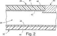
図2は、ウィンドウ28、間隙29、および材料32の拡大図である。ウィンドウ28は、上部保護コーティングまたは層40(任意)と、下部保護コーティングまたは層42とを有するフィルム41を含む。ウィンドウ28は金属格子(通常はヒバチと呼ばれる)(図示していない)によって支持され、この格子は支持体43に載せられる。保護コーティング40は真空チャンバー18と面しており、保護コーティング42はほぼ大気圧の雰囲気30と面している。下部保護層42は、雰囲気30の一部の成分(例えば酸素)のイオン化によって始まるフィルム41のフリーラジカル劣化を抑制する。フィルム41がポリマー材料である場合は、フリーラジカル酸化からの防護は耐用寿命に関して特に有用であり、より耐用寿命の短いウィンドウよりも実用的になる。保護層40および42は、フィルム41に沿った熱伝導性も向上させることができ、それによって照射中にウィンドウ28からの過剰の熱の放散を促進することができ、フィルム41の幅全体にわたる温度差と関連するひずみを減少させることができる。さらに、保護層40および42が十分伝導性であれば、保護層が電荷を放散することによって、フィルム41の絶縁破壊に対する抵抗性を増大させることができる。
【0035】
ウィンドウフィルム41は、低損失ビーム経路を形成できる単位経路を有する任意の材料を含むことができる。言い換えると、ウィンドウを透過するビームの深さ/線量曲線の吸収ピークを、照射される材料のコーティング層に移動させることが可能となるのに十分小さな単位路程を、ウィンドウフィルムが有する。好適なウィンドウ材料としては、アルミニウム、チタン、ベリリウム、窒化ホウ素、窒化ケイ素、およびケイ素が挙げられる。金属製フィルムを含む一部のウィンドウは、強度および可撓性に依存して2μm以下の薄さであってよい。このような材料の一部は従来の電子ビームウィンドウで使用されている。しかしながら、低損失ビーム経路で有用となるためには、これらは(従来のウィンドウと比較して)比較的小さい単位路程が得られる厚さである必要がある。例えば、公称12μmのチタンウィンドウが従来の電子ビーム発生器で使用されている。これらに使用されている公称12μmのチタンウィンドウは、実際の厚さは約13.97μmであることを本発明者らは発見した。本発明の場合、好適なチタンウィンドウの実際の厚さは12〜4μmとなりうる。ポリイミドフィルムを含めた種々のポリマーフィルムは、単位路程が小さいウィンドウ箔材料として特に好適である。例えば、ウィンドウ箔41としては、公称厚さ25μmのポリイミドフィルム、例えば、ピロメリット酸二無水物と4,4’−ジアミノジフェニルエーテルの重縮合反応で得られるポリイミドポリマーであるE.I.DuPont de Nemours and Co.(Wilmington、デラウェア州)より入手可能なKAPTON HNを挙げることができ、この両面にスパッタコーティングなどでアルミニウム蒸着したものは、実際の厚さが約27.43μmであり、単位路程が約36g/m2(gsm)である。他のDuPont Kaptonフィルムも好適となりうる。低損失ウィンドウとして有用となりうるその他のポリマー材料としては、熱安定性で耐久性(すなわち、高い引張強さと、応力緩和のために十分な延伸能力とを有する)のポリマー材料が挙げられる。好適なポリマーとしては、例えば、芳香族アミド、ポリスチレン、ポリスルホン、ポリフェニレンスルフィド、ポリエーテルイミド、およびポリウレタンを挙げることができる。好ましくは有用なポリマーウィンドウは単位路程が約3〜54gsmの間である。ウィンドウは約10μm〜40μmの間、好ましくは10〜30μmの間の厚さを有することができる。材料の耐久性がより高ければ、より薄いウィンドウであってもよい。より薄いウィンドウは単位路程がより短くなるので好ましい。ウィンドウは、真空チャンバー18の真空環境を収容するのに十分な強度を有する必要がある。
【0036】
好ましくは、ウィンドウ材料に適用される任意の保護コーティングは、電荷および熱の放散が可能であり、さらにフリーラジカル酸化に対して抵抗性を有する。電荷または熱の放散のみが可能なコーティングでは、フリーラジカル酸化も防護するコーティングの場合ほどウィンドウの耐用寿命は長くならない。二酸化ケイ素などのコーティング剤はウィンドウのポリマーフィルムに対する酸素の攻撃を抑制するが、電荷の放散は行わない。一方、例えば、アルミニウムなどの蒸着金属は、熱の放散、電荷の放散、およびフリーラジカル酸化の抑制が行える。しかしながら、金属コーティングはガス不浸透性となるために十分な厚さが必要であり、例えばアルミニウムの場合は約100nmの厚さが必要である。好適な蒸着方法は当業者には公知である。アルミニウム以外の好適な保護コーティング材料としては、例えば、ニッケル、クロム、および金が挙げられる。
【0037】
さらに、保護金属コーティングは、金属コーティングが非導電性となったりガス透過性となったりすることがある望ましくない酸化を防止するために、保護金属コーティング自身にコーティングが行われる場合がある。例えば、二酸化ケイ素コーティングはアルミニウムの酸化を防止する。保護コーティング40および/または42に必要なことは、ポリマーフィルムのフリーラジカル劣化の原因となるガスの拡散を実質的に防止するために十分となる材料の種類および厚さのみである。低電子吸収性ウィンドウを使用することによって、比較的低電圧の電子ビームでさえも、わずかな出力の低下のみでウィンドウ28を透過することができる。これによって、材料32の劣化性基材46には有害な線量を供給せずに材料32のコーティング44の改質に十分な線量を供給するのに十分な強度で材料32に照射するのに好適な深さ/線量曲線を有する電子ビームを発生させることができる。
【0038】
コーティングされた基材などの照射材料の断面を透過する線量分布または勾配は、ビーム源からの距離の各増分における電子ビーム線量を、ビームが横断する各材料の単位路程に対してプロットすることによって求めることができる。これを図4B〜4Eに示す。
【0039】
線量分布は、電子ビーム源からある距離離れた時に最大またはピーク線量に到達し、路程が増加するにつれて減少する。公称厚さが約12μmであり単位路程が54gsmである従来のチタンウィンドウは十分なエネルギーを吸収するため、電圧が175kVを超えるまで増加しても深さ/線量曲線(すなわち線量分布)のピークがウィンドウ/間隙領域を超える領域まで移動することはない。通常、このより高い電圧では、平坦で幅広で照射材料を通過する際にゆるやかに減少する深さ/線量分布が形成される。したがって、コーティングを改質するのに十分な線量と、電子ビーム劣化性基材が損傷しうる過剰な線量とのバランスをとるのには無理が生じる。これは、このような線量分布の形状では、単に段階的に減衰する勾配の線量がコーティングと基材の両方に照射されるためである。対照的に、本発明の厚さ25μmのアルミニウム蒸着ポリイミドフィルムウィンドウは単位路程がわずか36gsmである。このためウィンドウの吸収するエネルギーがより少くなり、ウィンドウ領域を超えた部分にピーク吸収が得られる。エネルギー吸収がより少ないことによって、低電圧の使用が可能となり、急勾配で狭い深さ/線量曲線を得ることができる。このような急勾配の曲線では、好適な表面線量と界面線量の比は5:1まで高くなりうる。
【0040】
ビーム電圧と間隙距離を調整することによって、改質性コーティング層内に吸収ピークが入るように線量分布を操作可能である。さらに本発明に低損失ウィンドウ、好ましくはポリイミドウィンドウは単位路程がより短いので、より低い電圧を使用することができる。好ましくは、ウィンドウ、保護層、おおび間隙の全体の単位路程が約41gsm未満である。低電圧を使用することで、線量ピークを超えた後の線量分布の減衰を鋭くすることができる。その結果、基材内に向かって延在する線量勾配部分は急勾配となって、基材に供給される線量を小さくすることができ、そのため劣化を制限することができる。基材に吸収されるエネルギーは、好ましくはコーティング層に吸収されるエネルギーの40%未満であり、より好ましくは25%未満、最も好ましくは20%未満である。
【0041】
深さ/線量曲線のピークが別の領域に移行するとして本発明の現象を説明しているが、所与電圧では深さ/線量曲線は変化しない。しかしながら、所与の深さ/線量曲線では、電子ビームが通過する領域の単位路程を短くすることによって、単位路程で画定される後の領域が電子ビーム源に近づくように移行し、そのため吸収ピークに近づいていく。このことは、例えば、図4B、4C、および4Dを比較することによって説明される。これらの図から分かるように、ウィンドウと間隙の単位路程を減少させることによって、単位路程で表される接着剤層は電子ビーム源に近づくように移動する。
【0042】
モンテカルロコードは、照射される材料の種々の操作条件の影響を予測するのに有用な深さ/線量分布のシミュレートに使用すると好都合となりうる。これらの予測によって、照射材料の種々の深さにおける電子ビーム線量の予測および調整が可能となり、基材を劣化させうる過剰の線量を使用せずに基材上のコーティングを改質するのに十分な最適線量を求めることができる。好適なモンテカルロコードとしては、Integrated Tiger Series(ITS)、Electron Gamma Shower(EGS)、およびMonte Carlo Neutron−Proton(MCNP)が挙げられる。モンテカルロコードによって、線量と深さの間の好都合な関係を特定することが可能となる。モンテカルロコードの使用および関連する計算に関しては、Douglas E.Weiss、Harvey W.Kalweit、およびRonald P.KensekによるLow−Voltage Electron−Beam Simulation Using the Integrated Tiger Series Monte Carlo Code and Calibration Through Radiochromic Dosimetryに記載されており、これはIrradiation of Polymers(ACS Symposium Series 620,American Chemical Society,Washington DC 1996)の第8章である。深さ/線量分布の計算に使用することができる別の方法が米国特許第5,266,400号に開示されている。
【0043】
ウィンドウ材料の原子番号は、ビーム電圧が一定である場合さえも深さ/線量曲線の形状に影響しうる。単位路程が同じ2種類の材料の場合、原子番号のより大きな材料が電子をより散乱する。これによって電子ビーム源側に線量ピークが近づき、それでもなお所与の単位路程では同じ深さで電子があるため、ピーク後の勾配の負の傾きが減少する。図3は、公称厚さ8μmのチタンウィンドウと、保護アルミニウムコーティングを有する公称厚さ25μmのポリイミドウィンドウとの両方について、3つの異なるビーム電圧(100keV、125keV、および175keV)および一定間隙4μmで、ナイロンを通過する深さ/線量曲線をシミュレートした結果を示している。どちらのウィンドウも単位路程は36gsmである。図から分かるように、公称厚さ25μmのポリイミドウィンドウによって形成される深さ/線量曲線と比較すると、原子番号12である公称厚さ8μmのチタンウィンドウで形成される深さ/線量曲線は、ピーク線量が小さく勾配の減衰もより緩やかになる。したがって、路程が同じであるチタンウィンドウとポリイミドウィンドウで同じ界面線量が実現される場合でも、基材層に侵入するエネルギーを減少させるためには、ポリアミドウィンドウを使用すると好都合となりうる。
【0044】
本発明の低損失ウィンドウは、従来の電子ビーム発生器でも好都合に使用することができる。通常、特に厚い材料を硬化させる場合には、従来の電子ビーム発生器は電圧が約175kV〜上限約300kVで使用すると最も好都合である。本発明のウィンドウによって、広範囲の距離(すなわち深さ)で同じ表面線量/界面線量を達成可能となる。例えば、図3は分かるように、175kVにおいて、25μmのポリイミドウィンドウでは、電子ビーム源から2.54μmおよび190.5μm(0.1ミルおよび7.5ミル)の距離で約5.0メガ電子ボルト・cm2/g(MeV・cm2/g−ビーム源電子)の線量をえることができるが、公称8μmのチタンウィンドウでは2.54μmと127μm(線量約7MeV・cm2/g)でしか同一線量が得られない。高電圧範囲の用途としては、小さな中空管への侵入の向上、または厚いウェブ材料の硬化の深さの拡大を挙げることができる。
【0045】
本発明では、材料への照射に使用される電子ビーム放射線のエネルギーは、ある実施形態では約30〜150keVであり、別の実施形態では約50〜75keVであり、これは使用される設備に依存する。電子ビーム放射線エネルギーは好ましくは120keV未満であり、より好ましくは100keV未満であり、最も好ましくは90keV未満である。
【0046】
図4Aは、選択範囲の電圧における、モンテカルロコードで得た一連の深さ/線量到達曲線を示しており、水を透過して種々の深さに到達する線量をシミュレートしたものである。ここで水は原子番号の小さい標準的な単位密度材料の代表として使用しており、同様の密度と同様の原子番号の成分とを有するポリマーなどの材料を通過する場合のエネルギー損失の予測に好適である。このシミュレーションでは、電子を吸収するウィンドウや間隙が存在しないことを仮定した。
【0047】
本発明の低損失ウィンドウは、深さ/線量曲線を移動させその形状を変化させることができる。図4Aに示されるように、より低電圧の電子ビームは、より高電圧の電子ビームよりもピーク線量が大きく、分布がせまい。水の浮け取る総エネルギー量は低電圧では少ないが(各曲線の下の面積から計算)、エネルギーはより浅い部分で受け取っている。このため線量は、水の表面付近の狭い帯域に実質的に制限される。図4Aから分かるように、50keVにおける深さ/線量曲線では、電子ビームは、実質的に照射材料の0〜約35g/m2の間の深さに存在する。対照的に、本発明のエネルギー範囲の上限である130keVの電子ビームでは、深さ/線量曲線は水面から深さ95g/m2付近のピークまで緩やかに増加し、その後緩やかに減少して約210gsmで消滅する。
【0048】
ウィンドウを通過する低電圧電子の量が多くなり、そのため接着剤層に線量ピークを移動させることができるので、低損失ビーム経路は重要である。本発明の装置を使用すれば、間隙および/またはウィンドウの電子吸収を変動させることによって、コーティング層と基材層の深さと関連する深さ/線量曲線の位置を調整することができ、そのため、基材の劣化が防止される適切な深さで最適な電子線量がコーティングした基材に供給される。例えば、図4Aに示されるように、65keVのビームは、比較的薄いコーティング(60gsm)のコーティング厚さ全体を改質するのに十分な線量を供給することができる。この線量は実質的に約0〜60g/m2の間の深さに供給される。60gsmより深い部分にあるごくわずかな基材にしか電子ビーム放射線は供給されない。しかしながら、この例ではウィンドウと間隙の吸収を考慮していない(エネルギーを吸収しない真空であると仮定している)ことに注意されたい。実際の使用では、ウィンドウと間隙の吸収を補償するためにより高い電圧が必要となるが、図4Aと同様の表面線量が実現される。
【0049】
図4B〜4Eは、種々のウィンドウと間隙の組み合わせを使用して照射した代表的な感圧接着テープ構造体の断面を通過する深さ/線量曲線を示している。図4Bは、従来の公称厚さ12μmのチタンウィンドウ(実際の厚さ約14μm、単位路程は約57gsm)、一般的な50mm窒素間隙(単位路程約62gsm)、厚さ43μmの電子ビーム架橋性感圧接着剤(単位路程約40gsm)、および厚さ127μmの電子ビーム劣化性不織基材(単位路程約80gsm)を通過する深さ/線量曲線の形状を示している。
【0050】
図4Cは、従来の公称厚さ12μmのチタンウィンドウ、狭い厚さ4mmの窒素間隙(単位路程約5gsm)、厚さ43μmの電子ビーム架橋性感圧接着剤、および厚さ127μmの電子ビーム劣化性不織基材を通過する深さ/線量曲線の形状を示している。
【0051】
図4Dは、公称厚さ3μmの窒化ホウ素ウィンドウ(単位路程約6.8gsm)、狭い厚さ4mmの間隙、厚さ43μmの電子ビーム架橋性感圧接着剤、および厚さ127μmの電子ビーム劣化性不織基材を通過する深さ/線量曲線の形状を示している。
【0052】
図4Eは、アルミニウム蒸着した公称厚さ25μmのポリイミドフィルムウィンドウ(実際の厚さ約27μm、単位路程約36gsm)、狭い厚さ4mmの間隙、厚さ43μmの電子ビーム架橋性感圧接着剤、および厚さ127μmの電子ビーム劣化性不織基材を通過する深さ/線量曲線の形状を示している。
【0053】
上述のグラフから分かるように、本発明で使用される低電圧ビームによって形成される線量分布は、より高電圧のビームの場合よりも狭く急勾配である。この分布では、基材線量がコーティング線量よりも有意に少なくなる。また図4B〜4Eを比較すれば分かるように、ウィンドウの単位路程と間隙の厚さとの両方が、照射されたコーティングと基材とを通過する深さ/線量曲線に大きく影響する。
【0054】
特定の照射材料を通過する深さ/線量分布は、それぞれ異なる電圧の多数のビームを材料に照射することによって形作ることができる。照射材料が特定の深さで受け取る線量は、各ビームによって供給される線量の和となる。複数の電子ビームの組み合わせを使用して、照射される材料への照射パターンを最適化することができる。例えば、非常に分布の狭い低電圧ビームを使用して、コーティングと基材の界面には余分な線量を供給せずに、コーティング層の表面および/または内部に供給される線量を追加または増加することができる。照射される層が厚い場合は、種々の低電圧ビームを3回以上曝露して、より複雑な分布をえることができる。このような複数回の曝露は、複数の小型Eビームを操作ライン上に連続して配列するか、あるいは1つの電子ビーム源に照射材料を複数回通過させるかによって実現することができる。
【0055】
基材材料の劣化を防止するだけでなく、本発明は、コーティング/基材界面が、必要であれば2つの層が互いに接合するに十分な電子ビーム線量を受け取るようにするためにも有用となりうる。これは、コーティングと電子ビーム劣化性基材の間を強く接合する必要がある場合に重要となりうる。例えば、バッキングに接着剤が適用される場合は、接着剤がバッキングから離れないことが重要である場合が多い。本発明によって、バッキングが過剰の電子ビーム線量に曝露されずに接着剤とバッキング層の間が強く接合されるのに十分な電子ビーム放射線を接着剤の界面部分が受け取ることができる。
【0056】
図5は、実施例で議論される種々の操作条件における、図4B〜4Eと同じ接着剤および裏当て材による種々の深さ/線量勾配を示している。重要なのは間隙(例えば4mm)、ウィンドウ材料(PIは公称25μmポリイミドウィンドウを意味し、Tiは公称12μmチタンウィンドウを意味する)、および電子電圧である。種々のウィンドウ/間隙(および電圧)の組み合わせに関して、表面線量と界面線量の関係をより明確にするために、接着剤層とバッキング層の分布(各層における深さを単位μmで示している)は独立に示している。層の間の間隔は接着剤/バッキング界面を表している。比較を容易にするため、界面線量が20kGyとなるようにビームの電流を調整した。ウィンドウ/間隙の組み合わせの単位路程(材料の密度と厚さの積より求められる)が増加する場合には、接着剤層を通過する線量の勾配を許容範囲に維持するために適宜電圧を増加させた。適切な電圧は、図4B〜4Eに記載される方法を使用して図4Aから計算することができる。電圧が増加すると、バッキングが受け取る全線量が増大し、それによってバッキングの劣化も起こりやすくなる。この劣化はバッキングが受け取る全エネルギーと関連付けることができ、バッキングの深さ/線量曲線の下の領域で表される。本発明者らは、公称25μmのポリイミドウィンドウ、4mmの間隙、および電圧78kVを使用する低損失経路では、MIT屈曲試験(MIT Flex Test)によって測定した場合に測定可能な基材の劣化は認められないことを発見した(表6および7に示す)(この組み合わせのウィンドウ、間隙、および電圧を使用した場合に受け取られる全エネルギーを示す図5の曲線は、バッキングの深さ約30μmで0に近づくため、バッキングの界面から30μmまでで吸収されるエネルギーを計算することによってすべての比較を行った)。表7から分かるように、公称25μmウィンドウ(実際の厚さ約27μm)、4mmの間隙、および78kVの電圧の組み合わせでは、全エネルギー吸収はエネルギー吸収は約11.2mJ/cm2であった。MIT屈曲数が1212であることから明らかなようにバッキングの劣化は認められなかった。同じウィンドウ/間隙の組み合わせを電圧を上げて使用した場合、エネルギー吸収は25〜35mJ/cm2に増大し、MIT屈曲数が800の範囲内にあることから劣化も増大したことが分かった。バッキングに吸収されるエネルギーが10mJ未満となるウィンドウ材料、間隙、および電圧の組み合わせによって、MIT屈曲試験結果の良いテープが得られる。
【0057】
本発明は、研究した材料に限定されるものではない。例えば本発明は、電子ビーム劣化性バッキング上の非接着性電子ビーム改質性コーティング材料の改質に使用することができる。硬質コーティングまたはトップコートの形成に使用することができるアクリル類やビニル類などのエチレン系不飽和材料がこのような材料の例である。図4A〜4Eに示されるように、ウィンドウ材料と間隙距離の任意の組み合わせを、単位gsmで表現し、図4Aに示される曲線によって得られる情報と組み合わせると、図4Aと同じ線量勾配を実現するための目標電圧を計算することができる。
【0058】
図6は、モンテカルロシミュレーションに基づくテープ構造体を通過する深さ/線量曲線を示しており、ある範囲のウィンドウ材料および厚さ、ならびに一定間隙4μmを仮定している。図4B〜4Eで説明した方法を使用して、チタン、ベリリウム、窒化ケイ素、および地下ホウ素を含むウィンドウの場合について深さ/線量曲線を作成した。これらの曲線を、公称厚さ25μmのポリイミドウィンドウを電圧78kVおよび92kVで使用した場合の図5の深さ/線量曲線に適合させた。各曲線でほぼ同じ界面線量(20kGy)となるように計算を行った。図5と6から、表面線量と界面線量の比の相違を比較することができる。この比は、ウィンドウ材料、間隙、および電圧を選択することによって好都合に制御可能であることが分かる。図6は、ウィンドウの単位路程が短縮されると、接着剤層の深さ/線量勾配が最終的に減少し、線量ピークが接着剤層内に移動することを示している。例えば、厚さ3μmの窒化ホウ素ウィンドウを通過する65keVのビームの場合の深さ/線量勾配では、接着剤層における入射線量と射出線量がほぼ同じであり、入射線量は射出線量の5倍の25μmのポリイミドウィンドウを通過する78keVで観察される場合と同様に紙への侵入は同程度に最小限である。同様の入射/射出線量によって、基材の損傷を増大させることなく接着剤層の深さにおける改質(架橋など)のバランスを調節することができる。その結果、目的とする用途に合わせた性質を有するテープを得るために剥離や剪断などの接着特性のバランスを調整することができる。
【0059】
実施例で使用される接着テープ構造体などの本発明の一部の実施形態では、コーティング表面が受け取る電子ビーム放射線の強度は、基材表面が受け取る電子ビーム放射線の強度の1〜5倍の間となりうる。他の実施形態では、比が5:1まで高くなると、コーティング層の過架橋や劣化などコーティング層表面の改質に悪影響が生じる。テープ構造体の理想的な深さ/線量曲線は、最適のテープ特性を得るために必要な層を通過する線量分布が得られるウィンドウ材料と間隙距離の組み合わせを選択することによって決定することができる。紙製バッキングを有する感圧接着テープの代表的な測定特性は、例えば、5−ボンド(5−bond)(接着剤の凝集強さ)、保持力(低速剥離抵抗性)、およびMIT flex(耐折強さ試験、この値はバッキングの劣化の影響を受ける)が挙げられる。
【0060】
本明細書で具体的に開示したもの以外の電子ビーム改質性コーティング層と電子ビーム劣化性バッキングの組み合わせでは、所望の改質を実現するために最適となる電圧、間隙、および界面線量が異なる。しかしながら最適値は、本発明の教示内容に基づいて当業者によって決定可能であり、例えば使用する材料の厚さと密度を調べ、その情報を図4Aに適用することによって決定可能である。
【0061】
本発明の低損失経路は、製造中の材料の処理能力を向上させることができる。本発明の低損失経路は、電子とウィンドウおよび間隙材料との間の相互作用が、従来の電子ビーム経路よりも少ないため、コーティング層表面で有効となる線量がより多くなる。
【0062】
本発明を説明するために特定の実施例を使用したが、本発明は、記載される特定の実施形態の制限されるものではなく、添付の請求項の意図および範囲内にある変更、同等物、および代替物も包含している。
【0063】
実験
本発明の装置の操作に有効な要因を示すために以下の実験を実施した。表1〜5は、5種類の異なる目標コーティング/基材界面線量20kGy、40kGy、60kGy、80kGy、および100kGyにおける線量計の照射の結果をまとめている。ウィンドウ材料、電圧、間隙、および電流は、これらの変数を変化させることによる影響を評価するためにすべて変動させた。さらに、本発明により照射した材料の物理的性質を表6、7、および8に示す。従来の公称12μmのチタンウィンドウを使用して得た比較データも表に加えている。
【0064】
これらの実験では、不活性チャンバーを通過する幅6インチの支持体(ウェブ)を備えたEnergy Sciences,Inc.Model CB−175電子ビーム発生装置で放射線加工を実施した。コーティングされた基材の試料はウェブ上で3.1m/分の速度で移動させた。CB−175のチャンバー内の酸素量は50〜100ppmの範囲となるように制限した。CB−175のウィンドウとウェブ経路の間の標準窒素間隙(本来の設備を使用)18mmである。この窒素間隙距離を縮めるために、真空チャンバーとウィンドウ支持体の間にスペ−サーを入れた。例えば、厚さ4mmの窒素間隙を形成するために、真空チャンバーとウィンドウ支持体の間に厚さ14mmのスペ−サーを配置した。スペ−サーを取付けた後で、厚さ3ミリの薄型ウィンドウクランプを使用して、ウィンドウを電子ビーム発生器上に固定した。この薄型クランプは、本来の厚さ10mmの標準クランプの代用品として使用した。この代用品によって、クランプの先にある照射される基材までの間隔が適切となった。
【0065】
CB−175を較正するために、Far West Technologies,Inc.(Goleta、カリフォルニア州)より入手可能なラジオクロミック線量を含有するポリマーフィルムである45μmと10μmの2つの線量計を使用して広範囲の線量測定を行った。ポリイミドウィンドウとチタンウィンドウの両方について90〜180kVを10kVの増分で線量測定を行った。チタンウィンドウ材料(公称厚さ12μm)は厚さが13.97μmであることが分かり、ポリイミドフィルム(DuPontより入手可能であり公称厚さ25.4μm(1ミル)で販売されている現在入手可能なKAPTON HN(ピロメリット酸二無水物と4,4’−ジアミノフェニルアミンの重縮合で得られるポリイミドポリマー)と同等であると考えられる従来入手可能であったKapton E)は両面の厚さ100nmのアルミニウムコーティングを含めて厚さが27.43μmであることが分かった。すべての場合、10μmおよび45μmの線量計を3つずつを指標カードに取付け、これらを移動ウェブ上に取付けて、照射した。各線量計厚さについて各電圧の線量を、得られた3つの読取値を平均して求めた。CB−175の実際の出力を求めて調整するため、実際の計器の線量と表示される計器の電流の比較線量測定データを使用した。
【0066】
各電圧における個々の深さ/線量の関係を、3つの線量計のスタックの平均から求めた。10μm線量計のスタックは通常低電圧の場合に使用し、43.5μm線量計は高電圧、例えば約125kVを超える電圧の場合に通常は使用した。実際の電圧を、線量計スタックの段階的深さ/線量分布と、ある範囲の電圧にわたるこれらのスタックのモンテカルロシミュレーションとを比較することによって求めた。CB−175の実際の電子ビーム電圧は表示電圧との整合性が90%であったが、この情報を使用して修正した電圧値を得た。本明細書中のすべての電圧はこうして修正した電圧である。
【0067】
表6〜9に示される試験データを得るために、マスキングテープ試料を使用した。このテープは繊維性バッキング上に接着剤をコーティングしたものであった。この接着剤は、1種類以上の電子ビーム架橋性エラストマーと、1種類以上の粘着性付与樹脂とで構成され、その他の硬化剤は含まず、層の厚さは40.6μmであり比重は0.93であった。テープバッキングはセルロース系不織布であり、厚さは約107μmで比重は0.63であった。このテープは、バッキング上に接着剤層を押出成形して作製された。
【0068】
同一断面について、測定線量を、モンテカルロコードで得た計算線量と比較し、モンテカルロコードの予測の確証を行った。すべての計算は実際の材料の厚さを使用して行った(例えば、公称12μmチタンウィンドウは実際の厚さが約13.97μmであったので14μmを計算に使用し、公称厚さ25μmのKaptonウィンドウは実際の厚さが約27.43μmであったので27μmを計算に使用した)。本発明者らは、測定値と一致するシミュレーションを行うためには、公称厚さよりも実際の測定値を使用し、表示電圧よりも実際の電圧を使用することが重要であることを発見した。このことは特に低電圧で操作する場合に重要であると思われる。接着剤とバッキングの界面において20kGy、40kGy、60kGy、80kGy、および100kGyの線量を選択した電圧で得るために必要な電流を計算する場合にもモンテカルロコードを使用した。結果を表1〜5に示す。10μm線量計は接着剤表面を模倣したものであった。43.5μm線量計は接着剤全体を模倣したものであり、接着剤/バッキング界面を模倣するために使用した。ほとんどの場合、測定線量と計算線量の結果は互いに20%以内であり、ごくわずかの場合では理由は不明であるが差違が20%を超えた。このような高い誤差範囲、意図された電圧範囲(約150〜175キロボルト)未満と低電流(1ミリアンペア(mA)未満)で装置を操作することによって発生する不安定が特に原因となっていると思われる。
【0069】
表1は、目標界面線量20kGyを得るために必要な較正を示している。実施例1〜10は、100nmの保護アルミニウムコーティングを有する公称25μmポリイミドウィンドウの場合の、4mm、17mm、および47mmの間隙距離における20kGyの目標線量を示している。比較例11および12は、公称12μmチタンウィンドウの場合の間隙距離17mmにおける20kGyの目標線量を示している。実施例の電圧は、ポリイミドウィンドウの場合には最低78kV〜最高139kVで変動させ、チタンウィンドウの場合は114〜146kVで変動させた。電流も最大0.63mA〜最小0.22mAで変動させた(各ウィンドウ/間隙の組み合わせでこの範囲は変動した)。
【0070】
電圧が増大すると、深さ/線量勾配は減少する。これを補償するために電流を減少させて、各ウィンドウ材料について各電圧で同じ目標界面線量を得た。表1の実施例1では、78kVの電圧と0.63mAの電流を使用して、接着剤/バッキング界面における目標の20kGyの線量を得た。深さ10μmでの計算線量は76kGyであり、測定線量は59kGyであった。43.5μmでの計算線量43kGyであり、測定線量は29kGyであった。対照的に、表1の実施例4では87kVの電圧と0.27mAの電流を使用して、界面における目標線量の20kGyを得た。深さ10μmでの計算線量は32kGyであり、測定線量は26kGyであった。43.5μmでの24kGyであり、測定線量は14kGyであった。表1の実施例1と4を比較すると、電圧を増大させ電流を低下させると、10μmと43.5μmの両方において測定線量が低下することが分かる。同様の相関傾向が表1の他の実施例でも認められる。
【0071】
従来の公称12μmチタンウィンドウではなく公称25μmのポリマー(この場合はポリイミド)ウィンドウを使用する場合に、照射材料の表面付近(10μm)と、内部、例えば材料のコーティング/基材界面(43.5μm)の線量の差をより大きくすることが可能であることも表1は示している。このより大きな差は、照射材料内に吸収ピークが移動していることを示している。特に、表1を参照すると、実施例7と11はどちらも間隙が17mmであるが、実施例7では公称25μmポリイミドウィンドウを使用し、実施例11では公称12μmチタンウィンドウを使用している。ポリイミドウィンドウの方が単位路程は短い。実施例7では、深さ10μmにおける測定線量は深さ43.5μmにおける測定線量の約1.7倍であった。対照的に実施例11では、深さ10μmにおける測定線量は深さ43.5μmにおける測定線量の1.2倍をわずかに超える程度であった。したがって、低損失ポリイミドウィンドウを使用することで、照射材料の接着剤部分の線量が材料のバッキング部分の線量よりも増大し、それによって裏当て材の劣化を防止することができ、性能を向上させることができる。
【0072】
要約すると、表1は、目標界面線量20kGyにおける表面線量(10μm)と接着剤層(43.5μm)を通過する全線量と関係を示している。深さ/線量曲線のピークがウィンドウから離れて照射されるコーティング層内に移動すると表面線量が増大する。このようなことが起こるのは、ウィンドウおよび間隙領域の単位路程を減少させ、目標界面線量を達成またはこれに近づけるためにより低い電圧を使用する場合である。より低い電圧は、裏当て材を通過する線量勾配の鋭い減衰と相関がある。
【0073】
さらに、本発明によってより電圧でより高い線量を接着剤層が受け取ることができるため、コーティングされた基材は、公称12μmの金属製ウィンドウ、幅50mmの間隙、および同様の電圧設定を使用する従来のシステムよりも速く加工することができる。例えば表1の実施例3と比較例11とを比較することによってこの差を見ることができる。実施例3は公称25μmポリイミドウィンドウ、4mmの間隙、電圧82kV、および電流0.40mAを使用して、10μmにおいて29kGyの測定線量を得ている。比較例11は公称12μmチタンウィンドウ、17mmの間隙、電圧114kV、および電流0.41mAを使用して、10μmにおいて17kGyの測定線量を得ている。本発明は所与の電流でより高い表面線量を得ることができるため、電子ビーム発生器を最大電流で操作した場合でさえも照射される材料の処理能力がより高くなる。
【0074】
【表1】

以下の表2は、目標界面線量40kGyを達成するために間隙距離、ウィンドウ材料、電圧、および電流を変化させた場合の10μm線量計および43.5μm線量計の影響を示している。表1と同様に、表面付近の線量(10μm)と照射される接着材料全体を通過する線量(43.5μm)の間の最大の差は、低損失ウィンドウを使用した場合に実現する。特に、線量の最大の差は、厚さ100nmのアルミニウム保護コーティングを有する低損失公称25μmポリイミドウィンドウを小さい間隙距離と併用した場合に実現する。表2の実施例1は、ポリイミドウィンドウを4mmの窒素間隙と併用すると、10μm線量計で147kGyの測定線量が得られ、43.5μm線量計で70kGyの測定線量が得られることを示している。これらの結果は78kVの電圧と1.26mAの電流を使用して得られた。実施例2は、80kVの電圧と1.02mAの電流を使用しても、10μm線量計における測定線量121kGy、および43.5μm線量計における測定線量66kGyという同様の結果が得られることを示している。10μmと43.5μmの測定線量の差は、一般に間隙が増大と減少する。例えば、47mmの間隙に電圧139kVと電流0.49mAを使用した実施例10は、10μmと43.5μmにおける測定線量がそれぞれ39および41となっている。
【0076】
保護コーティングを有するポリイミドウィンドウを小さい間隙とともに使用した場合と、12μmチタンウィンドウを大きい間隙とともに使用した場合との対比は、表2の実施例3と11を比較すれば明らかである。ポリイミドウィンドウと4mmの間隙を使用した実施例3では、電圧82kVおよび電流0.80mAを使用して測定線量が10μm線量計で94kGy、43.5μm線量計で45kGyであった。対照的に、12μmのチタンウィンドウと17mmの間隙間隙により高い電圧の114kVと同じ電流0.81mAを使用した実施例11では、測定線量は10μm線量計で38kGy、43.5μm線量計で32kGyしかなかった。これらの実施例は、単位路程のより短いポリイミドウィンドウ/小さい間隙は、従来のチタンウィンドウ/大きな間隙と比べると、深さ/線量曲線の吸収ピークが電子ビーム源を離れ接着剤層に向かって移動することを示している。このように接着剤層により高い線量が供給されると、電子ビームの使用がより効率的になることを示している。これらの実施例の比較から、低損失ビーム経路は表面線量と界面線量の比が有意に高くなることも分かる。これは、バッキング層を通過する深さ/線量勾配がより急勾配の望ましい形状になっていることを示している。
【0077】
【表2】
表3、4、および5は、表1および2と同様の相関を示している。全体的には表3、4、および5は、低損失電子ビーム経路が使用され、特により低電圧で使用される場合に、コーティング層(10μm線量計(表面)および43.5μm線量計(界面)を使用して概算した)の表面線量と界面線量の比が高いことを示している。これらの表は、表示の低損失電子ビーム経路をより高い表面線量で使用すると、同様の電流設定の比較例と比較するとエネルギー効率が向上していることも示している。例えば、表3の実施例7は公称25μmのポリイミドウィンドウで0.86mAの電流を使用しているが、比較例12は従来の公称12μmのチタンウィンドウで0.88mAの電流を使用している。実施例7は測定表面線量(10μmにおいて)97kGyを得るために必要な電圧はわずか98kVであるのに対し、比較例12は測定表面線量53kGyを得るのに146kVの電圧が必要である。
【0079】
【表3】
【表4】
【表5】
線量測定以外に、照射マスキングテープ試料の性能特性を分析した。照射後に、試料の接着剤側を、テープバッキングの低接着バックサイズ側で直ちに覆った。すべての試料を、一定湿度/温度室(相対湿度50%、21℃)内で少なくとも48時間貯蔵した後に試験を行った。以下の標準試験に従って試料の試験を行った。
【0083】
(1)MIT flex試験。テープの幅12.5mmのストリップについてTinius Olsen Testing Machine Company(Willow Grove、ペンシルバニア州)製造のMIT Flex Tester Model #1を使用して試験を行った。テープが破断するまで、1.5kgの重りをつり下げた張力下で機械的にテープを固定した。各報告結果は3回の測定の平均値であり、値の変動は±20%であった。バッキングの劣化を、放射線未照射の含浸強化クレープ紙バッキングと屈曲繰返し数を比較することによって測定した。通常、未照射バッキングは1200回屈曲することができる。屈曲繰返し数が900〜1200回で、実質的に劣化が存在しない非常に良好な状態であると見なした。屈曲繰返し数が900〜600回の間のテープは、多くの現行用途では満足できると見なした。屈曲繰返し数が600〜300回のテープは、破壊または切断することなしに基材からテープを除去するなどの一部の現行用途では満足できると見なした。屈曲繰返し数が300回未満のテープは、ほとんどの用途では脆くて許容できないと見なした。
【0084】
(2)5−ボンド試験。5−ボンド試験では、つり下げ剪断試験によって接着剤の凝集強さを測定する。テープの幅12.5mmの2つのストリップの互いの接着剤部分を長さ12.5mmにわたって接合した。次に、接合領域上に4.4kgのローラーを6回通した。こうして接合したストリップの下端に、1000gの重りを備えるジグが垂直方向にぶらさがるように取付けた。ストリップが分離するまでに経過する時間を測定した(単位分)。いずれの場合も5000分後には試験を終了した。この実験で使用した接着剤−バッキングの組み合わせの場合、一般的に400分を超える時間は十分架橋していることを示し、一般的に400分未満の時間は架橋が不満足(不十分)であることを示す。
【0085】
(3)保持力。保持力試験では、所定の重りを取付けたテープが、水平位置に保持された研磨ステンレス板から分離するのに要する時間を測定する。長さ15cmで幅19.1mmのテープの一端(長さ10cm)を板に配置し、9.9kgのローラーで10cmの部分の上を6回通すことによって板に取付けた。次にテープを取付けた板を水平方向に配置し、テープの自由端が下方にぶらさがって90°の剥離角を形成するようにした。テープの自由端に200gの重りを取付けた。板からテープが分離するまでに要する時間を測定した(単位分)。保持時間が少なくとも30分であれば満足できると判断した。
【0086】
上記試験の報告結果は、それぞれ3回の測定の平均である。
【0087】
MIT屈曲試験、5ボンド、および保持力データは高い値が得られることが望ましい。高い値は、試験した試料が可撓性であり高い接合強さを有することを示す。
【0088】
以下の表6は、マスキングテープ試料のMIT屈曲試験データを示している。実施例の項の最初で述べたように、マスキングテープは繊維性バッキング上にコーティングした接着剤を含むものであった。窒素雰囲気中で、表1〜5に示されるウィンドウ材料、間隙距離、電圧、および電流を使用してテープ構造体に照射を行った。表6に示すMIT屈曲試験結果は、テープ試料の屈曲特性が、電子ビームの侵入深さ(電圧量と直接相関がある)および放射線強度(線量と直接相関がある)の両方の影響を受けることを示している。表6から分かるように、最も好都合な結果は、4mm間隙と公称25μmポリイミドウィンドウを100kV未満、特に80kV未満の電圧で使用し界面線量が20〜60kGyの場合と相関がある。表6からは、目標界面線量が100kGyの場合でさえも、MIT屈曲試験の数値がほぼ1000〜600の間にあることも分かる。さらに表6は、目標界面線量が20kGyと小さくても、使用される接着剤と裏当て材から満足の行く接着テープが形成されることを示している。
【0089】
【表6】
表7は図5に示すデータを表にしたものである。得られる深さ/線量曲線の電流を、4mmの窒素間隙と単位路程が36gsmである厚さ27μm(公称25μm)のポリイミドウィンドウとを使用して低損失経路で界面線量20kGyが得られるように調整した。接着剤面の過度の改質(例えば過架橋)を引き起こさずに20kGyの界面線量を得るためには、78kVが実際的な最低電圧となる。なぜなら、これより低い電圧では表面線量と界面線量の比が5:1を超え、表面の過剰な改質が起こる可能性があるからである。78kVの電圧では、MIT屈曲試験サイクル数が1212であることから分かるように紙の劣化は検出されなかった。ウィンドウ、間隙、および界面線量の同じ組み合わせで電圧が増大すると、全体的な傾向として屈曲試験数が減少し、これはバッキングの劣化が増大していることを示している。バッキングの劣化は、電圧が増加すると増大し、間隙が4mmから17mm、さらには47mm(これは市販の電子ビームに一般的な50mmの間隙に近い)に変更すると増大した。従来の厚さ14μmのチタンウィンドウと17mmの間隙(電圧114kVおよび146kVにおいて)を使用する場合にもバッキングの劣化が増大した。
【0091】
表7の屈曲試験数で示される劣化は、裏当て材の最初の30μmが吸収した全エネルギーと大まかな相関がある。吸収した全エネルギーは、図5の深さ/線量曲線の下の領域で表される。表7から分かるように、バッキングの最初の30μmによる約11.2mJ/cm2程度のエネルギー吸収では劣化は起らなかった。約25〜35mJ/cm2が同じ距離で吸収された場合は、劣化がより顕著となった(屈曲数が約700〜800サイクルに減少)。したがって、バッキング層の最初の30μmに吸収されるエネルギーを約40mJ/cm2未満に維持することが好ましい。
【0092】
表7
バッキングのエネルギー吸収と屈曲試験数の関係
表8は5−ボンド試験データを示している。5−ボンド結果は、電圧とは独立に界面線量の関数となった。最終的に5000分を超えるまでは、線量が増大すると、すべてのウィンドウ、間隙、および電圧条件で5−ボンド結果が増大した。試料が5000分を超えた時には試験を終了した。したがって、表8は、一定の目標界面線量で電圧を調整することによってテープの5−ボンド特性を制御可能であることを示している。約500分の結果を得るためには通常は20kGyの線量で十分であったし、約5,000分の結果を得るためには通常は40kGyの線量で十分であった。
【0094】
【表8】
表9は保持力試験結果を示している。予想されるように、保持力は表面線量の影響を非常に大きく受けると思われる。目標界面線量が増大すると、表面線量も増大し、保持力は低下する。全体的なデータの傾向から、より低い保持力がより高い界面線量と相関があることが分かる。表1〜5から分かるように、約92kV未満の電圧では、界面線量に対して高い表面線量を得ることができる。このため、過剰な硬化や過架橋などの過剰な改質が表面に起る場合があり、これが保持力の低下の原因となりうる。
【0096】
【表9】
表6、8、および9のデータは、低損失経路の場合には広範囲の電圧/線量の組み合わせで、性能の要求を満たすマスキングテープを作製することが可能であることを示している。90kV以下の低電圧における低損失ビーム経路によって、ほとんどの用途の最小要求を超えるテープ特性を得ることができる。
【0098】
その他の本発明の実施形態は、請求項の範囲内にある。明細書および実施例は単に例示を意図しており、本発明の完全な範囲および意図は請求項によって示される。
【図面の簡単な説明】
【図1】 本発明の実施形態により構成され配置された電子ビーム源の断面詳細図である。
【図2】 本発明の実施形態により構成され配置された低損失ウィンドウの断面拡大図である。
【図3】 8μmのチタンウィンドウ、および100nmの保護コーティングを有する25μmのポリイミドウィンドウ(どちらも単位路程は36g/m2)を使用し、電子ビーム電圧100kV、125kV、および175kVを使用した場合の、ナイロンを透過する放射線の深さ/線量の傾きをシミュレートしたグラフである。
【図4A】 水を透過する場合の放射線量対単位路程を異なる電圧でシミュレートしたグラフである。
【図4B】 従来の公称12μmのチタンウィンドウ、従来の窒素間隙、および接着テープを透過する場合の放射線量対単位路程を異なる電圧でシミュレートしたグラフである。
【図4C】 従来の公称12μmのチタンウィンドウ、小さな窒素間隙、および接着テープを透過する場合の放射線量対単位路程を異なる電圧でシミュレートしたグラフである。
【図4D】 公称3μmの窒化ホウ素ウィンドウ、小さな間隙、および接着テープを透過する場合の放射線量対単位路程を異なる電圧でシミュレートしたグラフである。
【図4E】 保護コーティングを有する公称25μmのポリイミドウィンドウ、小さな間隙、および接着テープを透過する場合の放射線量対単位路程を異なる電圧でシミュレートしたグラフである。
【図5】 異なる間隙距離、ウィンドウ材料、および電圧を使用した場合の、図4B〜4Eの接着テープを透過する電子ビーム放射線の線量対深さをシミュレートしたグラフである。表面線量と界面線量の比の比較が可能となる目標界面線量20キログレイ(kGy)を得るために電流を調整することで、すべての電子ビームの計算を規格化した。
【図6】 種々の電圧とウィンドウ材料の組み合わせ、ならびに4mmの一定間隔の場合の、図4B〜4Eの接着テープを透過する線量/深さ曲線をシミュレートして比較したグラフである。表面線量と界面線量の比の比較が可能となる目標界面線量20kGyを得るために電流を調整することで、すべての電子ビームの計算を規格化した。[0001]
Field of Invention
The present invention is directed to a method and apparatus for irradiating an electron beam onto a single-layer or multilayer article and the resulting product. More particularly, the present invention is directed to the use of a low loss electron beam path to irradiate an electron beam modifying material coated on an electron beam degradable substrate.
[0002]
background
In recent years, the use of electron beam radiation to modify various materials such as polymerizable materials, crosslinkable materials, graft materials, and curable materials has increased. For example, electron beam processing can be used to polymerize and / or crosslink various pressure sensitive adhesive formulations coated on a film substrate, graft the coating onto the substrate, and various liquid coating agents such as printing inks. Has been used to cure. If an electron beam is used to modify the material, a coating solution such as a coating solution containing a volatile organic compound (“VOC”) becomes unnecessary. Thus, VOC emissions can be reduced, energy costs can be reduced, and environmental or occupational risks can be reduced.
[0003]
Unlike ultraviolet (“UV”) radiation, which is also used for crosslinking, polymerization, grafting, and curing various materials, electron beam radiation does not require the use of an initiator. In addition, electron beam radiation is readily absorbed by all organic materials and is not easily modified by UV radiation, such as thick and opaque materials, as well as UV modifications such as allylic, olefinic, and unsaturated compounds. Are easily absorbed by materials that are resistant to. Polyethylene is a representative of unsaturated compounds that cannot be easily cured by UV radiation, but can be cured by electron beam radiation.
[0004]
While electron beam radiation has many advantages, it also has some limitations. As such a restriction, the conventional electron beam generating equipment is relatively expensive. This expense is at least partially related to the need for large power supplies, lead shields, high voltage devices, and safety monitoring devices. In recent years, manufacturers have been able to produce lower-priced, smaller and lighter electron beam equipment by reducing the electron beam voltage to below 125 kilovolts (kV). See, for example, Energy Sciences, Inc. (Wilmington, Massachusetts), Advanced Electron Beam Technologies, (Wilmington, Massachusetts), and American International Technologies, Inc. (Torrance, CA) is a manufacturer of small, low-cost electron beam generating equipment. If these apparatuses are used, the purchase cost and operation cost of the electron beam radiation equipment can be reduced.
[0005]
Another major limitation of electron beam radiation is that electrons often penetrate too deeply into the material being irradiated. High voltages are often used to obtain a reasonably uniform dose across the entire cross section of the electron beam modifying coating, which allows for a significant amount of high energy electrons in the layers below the electron beam modifying coating. May invade. This is a problem in the case of multilayer materials that include a coating of the material to be modified and a substrate or backing of the material that can be damaged by electron beam radiation. Paper, polyvinyl chloride, polypropylene, and TEFLON are all materials that are often used as adhesive substrates, but are susceptible to degradation by electron beam radiation. Electron beam radiation may cause the substrate to become brittle or cause other degradation. As a result, the base material deteriorates, and the quality of the product decreases, or it cannot be used in a desired application.
[0006]
Summary of invention
Existing electron beam generation systems do not adequately address the problem of high equipment costs and the problem of sufficiently modifying the coating without degrading the substrate. Therefore, there is a need to control the electron beam irradiation such that the penetration of the electron beam is substantially limited to a particular layer of irradiated material, preferably just the electron beam modifying coating of the material.
[0007]
The present invention is directed to an apparatus and method for delivering electron beam radiation to a material, particularly a multilayer material having an electron beam modifying coating and an electron beam degradable substrate. The present invention is also directed to products manufactured using the apparatus and method of the present invention. In at least one embodiment of the present invention, the dose delivered to a particular depth of irradiated material (energy delivered per unit mass) can be controlled.
[0008]
One aspect of the present invention provides an electron beam source, a polymer film having at least two surfaces, a window in proximity to the electron beam source, a protection on at least one surface of the polymer window that is resistant to free radical degradation It is intended for an electron beam device comprising a layer, a support on which the material irradiated by the beam source is arranged and in close proximity to the window, and a gap between the window and the support.
[0009]
Another aspect of the invention is directed to a window comprising a polymer film having at least two surfaces and used in conjunction with an electron beam source, the film comprising at least one protective layer that is resistant to free radical degradation. On the surface, this film has 10 -4 An environment having a pressure below Torr can be accommodated.
[0010]
Another aspect of the present invention is a step of providing an electron beam source and a window for use with the electron beam source, having at least two surfaces and resistant to free radical degradation on at least one surface. The invention is directed to a method of irradiating an article with an electron beam comprising providing a window comprising a polymer film having a protective protective layer and irradiating the article with electrons from an electron beam source through the window.
[0011]
Another aspect of the invention provides an article having an electron beam modifying first layer and an electron beam degrading second layer proximate to the first layer, energy, voltage, And providing an electron beam source with an adjustable amount of current and providing a window between the electron beam source and the article to be illuminated, wherein there is a gap between the window and the article, The unit path of the window is 3-50g / m 2 The step of setting the energy of the electron beam source between 50-150 keV and the electron beam source so that the electron beam can modify the first layer without substantially degrading the second layer. Modifying the properties of an article having two or more layers, including adjusting voltage and current, adjusting a gap distance between the window and the article, and irradiating the article with an electron beam from an electron beam source The purpose is to do.
[0012]
Another aspect of the present invention is an electron beam modified article comprising an electron beam degradable backing material and a coating modified with the electron beam and on the backing material, adjacent to the modified coating. 30μm of the electron beam degradable backing 0.1-40mJ / Cm 2 An electron beam modified article that absorbs the energy of the present invention is provided.
[0013]
Another aspect of the present invention is an electron beam modified article comprising an electron beam degradable backing material and a coating modified with the electron beam and on the backing material, wherein the modified coating is delaminated. An electron beam modified article that is not contaminated with material is provided. According to the present invention, the electron beam modifying layer can be modified (eg, cured) directly on the electron beam degradable backing without substantially degrading the backing so that it can be modified on a release material such as silicone. There is no need to modify the layer and later transfer it to the backing. This eliminates the possibility of the modifying layer being contaminated with the release material.
[0014]
When irradiating an electron beam modifying material coated on an electron beam degradable substrate, it is important that the irradiation material is irradiated with a dose at which the modifying layer is sufficiently modified and transmitted through the material. Yes, doing so makes it useful for the intended purpose, and the material adheres to the substrate. However, it is also important that the dose not be excessive. For example, when irradiating an adhesive layer on a substrate, the surface dose needs to be sufficient to impart important adhesive properties such as cohesive strength and adhesive strength, The dose should not be so high that excessive modification such as degradation (which limits the adhesive properties of the adhesive layer) occurs. The dose also needs to be sufficient to sufficiently modify the adhesive at the adhesive / substrate interface, thereby bonding the adhesive to the substrate. However, the dose at the interface should not be so high that the substrate is significantly degraded.
[0015]
The electron beam apparatus of the present invention comprises an electron beam source constructed and arranged to direct electrons to a material, most preferably a multilayer material having both an electron beam modifying upper layer and an electron beam degrading lower layer. Is provided. When electrons move from the electron beam source, they pass through a vacuum environment, pass through a window foil with low electron absorption properties (a “low loss” window), and move to an atmospheric pressure environment that includes the irradiated material. The path of the electron beam that passes through the low loss window from the electron beam source and reaches the irradiated material is also referred to herein as the low loss path. By using a low-absorption window, even a relatively low voltage electron beam can be transmitted through the window with a slight decrease in power. The resulting electron beam can penetrate into the coating of the irradiated material and modify the coating, preferably without penetrating or degrading the substrate.
[0016]
Suitable window materials for use in the low loss path include polymer films such as polyimide films. In order to improve performance and durability by reducing free radical degradation, a protective layer is disposed on at least the window surface facing the atmospheric pressure environment. The protective layer may be a thin layer of aluminum or other metal that protects against free radical degradation. Preferably, the protective layer also improves electrical and thermal conductivity along the film.
[0017]
After the electrons pass through the window, they pass through the gap between the window and the irradiated material. This gap typically contains nitrogen gas or another inert material maintained at approximately atmospheric pressure. In order to increase the dose of electron beam radiation delivered to the modifying coating and reduce the dose absorbed by the gap electrons, the gap distance is preferably minimized. Reducing the gap distance also increases the energy efficiency of the device, thereby lowering the voltage used to irradiate the material. In some embodiments, the gap between the window and the irradiating material is about 2-100 mm, in another embodiment 4-50 mm, and in yet another embodiment about 5-20 mm. The preferred gap size depends on factors such as the window material, the presence of the window clamping structure, the voltage used, and the thickness of the modifying layer.
[0018]
As the electron beam passes through the window, gap, coating, and any substrate layer, the amount of electron energy absorbed by these regions can be determined and plotted as a depth / dose curve, which is The absorbed dose is plotted against the distance from the electron beam source. The magnitude of this curve can vary depending on many conditions, but usually has a peak where energy absorption is maximized. In conventional electron beam systems, this peak often exists in the window or gap region. The ideal depth / dose curve has a square wave shape where no energy is absorbed in the window and gap, the modifiable material layer absorbs a uniform amount of energy throughout its thickness, and the degradable substrate is Does not absorb energy.
[0019]
The principle advantage of the low loss beam path is that the absorption peak of the depth / dose curve, also referred to in the art as the “backscatter” peak, so that the depth / dose curve approaches a more ideal square wave curve, It is possible to move from the window / gap region to the coating region. At the same time, the lower voltage enabled by the low loss beam path characteristics results in a depth / dose curve with a sharp negative slope across the penetration depth remaining after the absorption peak. Thus, if the choice of window material and gap distance is appropriate, a depth / dose curve having a decaying slope that can approximately match the substrate / coating interface is obtained.
[0020]
According to the present invention, the dose received by the coating can be much higher than the dose received by the substrate, since the electron beam radiation dose can rapidly decay upon entering the irradiated material. The ratio of the total dose received by the substrate is affected by factors such as the shape of the depth / dose curve, the window material, the gap distance, the voltage required to sufficiently modify the coating, and the thickness of the substrate. In some embodiments, the dose can be 1-5 times greater on the coated surface than on the coating / substrate interface. The acceptable value for the ratio of surface dose to interface dose is highly dependent on the amount of radiation that the coating layer can receive without causing excessive modification such as degradation or overcrosslinking.
[0021]
Conventional electron beam paths, such as those with a 12 μm titanium window and operated at voltages higher than about 150 kV, generally provide a relatively flat and wide depth / dose curve. If a high surface dose is used, a substantial amount of substrate degradation can occur because the interface dose and the total dose to the substrate usually increase as the surface dose increases. Surprisingly, we can obtain a relatively high but narrow depth / dose curve with a low loss beam path, in which case the interface dose is not necessarily high due to the high surface dose. I found it not. Thus, an electron beam modifying layer such as an adhesive layer can be successfully modified with an electron beam dose 5 times greater on the coating surface than on the coating / substrate interface. The shape and placement of the depth / dose curve obtained in the low loss path can provide sufficient dose to the adhesive layer, and sufficiently modify the interface while minimizing the penetration of the electron beam into the substrate. Can be adhered to adjacent substrates.
[0022]
In order to improve the predictability of the dose of electron beam radiation at various depths of irradiated material, Monte Carlo code can be used to predict depth and dose values based on window material and gap distance. it can. Such prediction facilitates adjustment of the electron beam dose at various depths of the irradiated material and allows the optimum dose to be sent to the coating for modification without damaging the substrate. The electron beam radiation used to irradiate the coated substrate is preferably operated at a voltage of about 30-150 kV, more preferably about 50-100 kV, and most preferably about 50-75 kV. By selecting the voltage, the shape of the depth / dose distribution (and thus the ratio of surface dose to interface dose) can be determined. If the current is selected, the actual dose irradiated to the irradiated material can be determined. By adjusting the current, for example, the interface dose can be changed.
[0023]
The present invention is further directed to products, specifically electron beam modified articles. The product can include one or more electron beam modifying layers. In some embodiments, the article includes one or more electron beam modifying coating layers on an electron beam degradable substrate. The invention includes embodiments in which the electron beam degradable substrate exhibits acceptable or minimal electron beam degradation after irradiation or does not exhibit electron beam degradation. The target interfacial dose is that which allows the coating to adhere to the substrate so that degradation can be minimized and a usable tape product can be made.
[0024]
The above summary is not intended to describe every embodiment of the present invention. Other aspects and advantages of the present invention will become apparent upon reading the following description and detailed description of the drawings.
[0025]
Detailed description
One aspect of the present invention is directed to an apparatus for irradiating a material with an electron beam. The present invention is also directed to a method of irradiating a material such as a multilayer material having a coating suitable for electron beam irradiation and a substrate easily damaged by electron beam irradiation. The present invention provides a coating with sufficient radiation to promote beneficial modification of the material, such as curing, grafting, polymerization, and / or crosslinking, without causing excessive irradiation of the substrate or degradation of the substrate. Can be irradiated.
[0026]
FIG. 1 is a detailed view of an apparatus comprising an electron beam source 10 (one E-beam source is shown) constructed in accordance with the present invention. When a high voltage from the high
[0027]
The
[0028]
The
[0029]
The present invention provides an improved method and apparatus for controlling the penetration of electrons from the
[0030]
To provide a relatively high dose for the coating material and at the same time a relatively low dose for the substrate material, a device with a
[0031]
The unit path length is the density of the material through which the electron beam is transmitted (g / cm 3 (G / cc)) and the transverse distance (μm) (usually the thickness of the material), in units of g / m 2 (Gsm). For example, the unit path of nitrogen gas having a density of about 0.00125 g / cc at a standard temperature and a standard pressure is 5 gsm when the gap distance is 4 mm, 25 gsm when the gap is 20 mm, and the gap is 50 mm. The case is 62.5 gsm. A nominal 12 μm titanium window has a unit path length of 54 gsm. As can be seen, the large air gap can greatly reduce the transmission of electrons at lower voltages than conventional titanium windows.
[0032]
Unit path length is conventionally used to compare the relative mass stopping power of various material combinations (with different densities and thicknesses) on a single scale for a particular voltage. Mass stopping power is the average energy loss per unit path. The mass stopping power of the material through which accelerated electrons pass is affected by the beam voltage. In general, mass stopping power is also directly related to the density, thickness, and atomic number of the material through which the electron beam passes. In the case of the present invention, such materials can include low loss windows, gaps, coatings, and substrates.
[0033]
The present invention provides an apparatus and method for improving the ability to control the depth / dose distribution of an electron beam, in particular a low voltage electron beam with an energy of less than 150 keV, and even an electron beam with an energy of less than 75 keV. In general, this is done by reducing the amount of electron beam energy that is absorbed before reaching the irradiated material. The present invention provides a low loss window that preferably includes a polymeric material and allows significant and convenient changes and adjustments in depth / dose penetrating the irradiated material by using the window while controlling the gap size Teach the method. The amount of electron beam energy to modify the electron beam modifying coating by using a gap having a specific unit path and a window material having a path length smaller than a conventional titanium window with a nominal thickness of 12 μm, for example. While increasing the ratio, the shape of the depth / dose distribution can be changed so that significant degradation of the underlying electron beam degradable substrate can be avoided. For example, if a polyimide window with a nominal thickness of 25 μm deposited with aluminum is operated at a voltage of 90 kV in combination with a nitrogen gap of 2 mm, a titanium window with a nominal thickness of 12 μm is used at 125 kV with a nitrogen gap of 5 cm. Twice as much energy as when operated can reach the coating surface. Even if the metal is deposited on the polyimide, the coating is very thin (about 100 nm) and its unit path is negligible (less than 0.5 gsm on all surfaces deposited), so it has little effect on the unit path. do not do.
[0034]
FIG. 2 is an enlarged view of
[0035]
The window film 41 can include any material having a unit path that can form a low loss beam path. In other words, the window film has a unit path that is small enough to allow the absorption peak of the depth / dose curve of the beam passing through the window to move to the coating layer of the irradiated material. Suitable window materials include aluminum, titanium, beryllium, boron nitride, silicon nitride, and silicon. Some windows containing metal films may be as thin as 2 μm or less depending on strength and flexibility. Some of these materials are used in conventional electron beam windows. However, in order to be useful in low loss beam paths, they need to be of a thickness that allows a relatively small unit path length (compared to conventional windows). For example, a nominal 12 μm titanium window is used in conventional electron beam generators. The inventors have discovered that the nominal 12 μm titanium windows used in these have an actual thickness of about 13.97 μm. In the case of the present invention, the actual thickness of a suitable titanium window can be 12-4 μm. Various polymer films including a polyimide film are particularly suitable as a window foil material having a small unit path. For example, as the window foil 41, a polyimide film having a nominal thickness of 25 μm, for example, a polyimide polymer obtained by polycondensation reaction of pyromellitic dianhydride and 4,4′-diaminodiphenyl ether is used. I. DuPont de Nemours and Co. KAPTON HN available from (Wilmington, Delaware) can be mentioned, and the actual thickness is about 27.43 μm and the unit path length is about 36 g / m. 2 (Gsm). Other DuPont Kapton films may also be suitable. Other polymeric materials that may be useful as a low loss window include thermal stable and durable polymeric materials (ie, having high tensile strength and sufficient stretch capacity for stress relaxation). Suitable polymers can include, for example, aromatic amides, polystyrene, polysulfone, polyphenylene sulfide, polyetherimide, and polyurethane. Preferably useful polymer windows have a unit path between about 3 and 54 gsm. The window may have a thickness between about 10 μm and 40 μm, preferably between 10 and 30 μm. A thinner window may be used if the material is more durable. Thinner windows are preferred because the unit path is shorter. The window needs to be strong enough to accommodate the vacuum environment of the
[0036]
Preferably, any protective coating applied to the window material can dissipate charge and heat, and is resistant to free radical oxidation. For coatings that can only dissipate charge or heat, the useful life of the window is not as long as for coatings that also protect free radical oxidation. Coating agents such as silicon dioxide inhibit oxygen attack on the window polymer film, but do not dissipate charge. On the other hand, for example, a deposited metal such as aluminum can dissipate heat, dissipate charges, and suppress free radical oxidation. However, the metal coating needs to be sufficiently thick to be gas impermeable, for example about 100 nm in the case of aluminum. Suitable vapor deposition methods are known to those skilled in the art. Suitable protective coating materials other than aluminum include, for example, nickel, chromium, and gold.
[0037]
Furthermore, the protective metal coating may be coated on the protective metal coating itself to prevent unwanted oxidation that may render the metal coating non-conductive or gas permeable. For example, a silicon dioxide coating prevents the oxidation of aluminum. All that is required for the
[0038]
The dose distribution or gradient through a cross-section of irradiated material, such as a coated substrate, is obtained by plotting the electron beam dose at each increment in distance from the beam source against the unit path of each material traversed by the beam. Can be sought. This is shown in FIGS.
[0039]
The dose distribution reaches a maximum or peak dose at some distance from the electron beam source and decreases as the path length increases. A conventional titanium window with a nominal thickness of about 12 μm and a unit path length of 54 gsm absorbs enough energy, so that the peak of the depth / dose curve (ie, the dose distribution) will increase even when the voltage is increased to over 175 kV. There is no movement beyond the window / gap area. Typically, this higher voltage produces a depth / dose distribution that is flat, wide, and gradually decreases as it passes through the irradiated material. Therefore, it is unreasonable to balance the dose sufficient to modify the coating with the excess dose that can damage the electron beam degradable substrate. This is because with such a shape of the dose distribution, both the coating and the substrate are irradiated with a dose that gradually decreases in a stepwise manner. In contrast, the 25 μm thick aluminum deposited polyimide film window of the present invention has a unit path length of only 36 gsm. For this reason, the energy absorbed by the window is reduced, and peak absorption is obtained in a portion beyond the window region. Less energy absorption allows the use of low voltages and can yield steep and narrow depth / dose curves. With such steep curves, the preferred surface dose to interface dose ratio can be as high as 5: 1.
[0040]
By adjusting the beam voltage and the gap distance, the dose distribution can be manipulated so that an absorption peak is in the modifying coating layer. In addition, lower voltage windows, preferably polyimide windows, can be used in the present invention because the unit path is shorter. Preferably, the overall unit path of the window, protective layer, and gap is less than about 41 gsm. By using a low voltage, the attenuation of the dose distribution after exceeding the dose peak can be sharpened. As a result, the dose gradient portion extending toward the inside of the base material becomes steep and the dose supplied to the base material can be reduced, so that deterioration can be limited. The energy absorbed by the substrate is preferably less than 40% of the energy absorbed by the coating layer, more preferably less than 25% and most preferably less than 20%.
[0041]
Although the phenomenon of the present invention has been described as the peak of the depth / dose curve shifting to another region, the depth / dose curve does not change at a given voltage. However, for a given depth / dose curve, by shortening the unit path of the region through which the electron beam passes, the subsequent region defined by the unit path shifts closer to the electron beam source, and therefore the absorption peak. Approaching. This is illustrated, for example, by comparing FIGS. 4B, 4C, and 4D. As can be seen from these figures, by decreasing the unit path of the window and the gap, the adhesive layer represented by the unit path moves closer to the electron beam source.
[0042]
The Monte Carlo code may be advantageous when used to simulate depth / dose distributions useful for predicting the effects of various operating conditions on the irradiated material. These predictions allow for the prediction and adjustment of electron beam doses at various depths of irradiated material, sufficient to modify the coating on the substrate without using excessive doses that can degrade the substrate. Optimal dose can be determined. Suitable Monte Carlo codes include Integrated Tiger Series (ITS), Electron Gamma Shower (EGS), and Monte Carlo Neutron-Proton (MCNP). The Monte Carlo code makes it possible to identify a favorable relationship between dose and depth. For the use of Monte Carlo code and related calculations, see Douglas E .; Weiss, Harvey W. Kalweit, and Ronald P. Low-Voltage Electron-Beam Simulation Using the Integrated Tiger Series Monte Carlo Code and Calibration Through Radiochromic are described in Dosimetry, which Irradiation of Polymers by Kensek (ACS Symposium Series 620, American Chemical Society, Washington DC 1996) eighth It is a chapter. Another method that can be used to calculate the depth / dose distribution is disclosed in US Pat. No. 5,266,400.
[0043]
The atomic number of the window material can affect the shape of the depth / dose curve even when the beam voltage is constant. In the case of two types of materials having the same unit path length, a material having a higher atomic number scatters electrons more. This brings the dose peak closer to the electron beam source side, and yet there is an electron at the same depth in a given unit path, thus reducing the negative slope of the slope after the peak. FIG. 3 shows that for both a titanium window with a nominal thickness of 8 μm and a polyimide window with a nominal thickness of 25 μm with a protective aluminum coating, nylon with three different beam voltages (100 keV, 125 keV, and 175 keV) and a constant gap of 4 μm. The result of simulating the depth / dose curve passing through is shown. In both windows, the unit path is 36 gsm. As can be seen, the depth / dose curve formed with a nominal 8 μm titanium window with
[0044]
The low loss window of the present invention can also be advantageously used with conventional electron beam generators. Usually, particularly when thicker materials are cured, conventional electron beam generators are most conveniently used at voltages from about 175 kV to an upper limit of about 300 kV. The window of the present invention allows the same surface dose / interface dose to be achieved over a wide range of distances (ie depths). For example, as can be seen in FIG. 3, at 175 kV, a 25 μm polyimide window is approximately 5.0 megaelectron volts at 2.54 μm and 190.5 μm (0.1 mil and 7.5 mil) distances from the electron beam source.・ Cm 2 / G (MeV · cm 2 / G-beam source electrons) can be obtained, but 2.54 μm and 127 μm (dose of about 7 MeV · cm for a nominal 8 μm titanium window) 2 / G), the same dose can only be obtained. Applications in the high voltage range can include improved penetration into small hollow tubes or increased depth of cure of thick web materials.
[0045]
In the present invention, the energy of the electron beam radiation used to irradiate the material is about 30-150 keV in one embodiment and about 50-75 keV in another embodiment, depending on the equipment used. To do. The electron beam radiation energy is preferably less than 120 keV, more preferably less than 100 keV, and most preferably less than 90 keV.
[0046]
FIG. 4A shows a series of depth / dose arrival curves obtained with a Monte Carlo code at a selected range of voltages, simulating doses that penetrate water and reach various depths. Here, water is used as a representative of standard unit density materials with small atomic numbers, and is suitable for predicting energy loss when passing through materials such as polymers having similar densities and components with similar atomic numbers. It is. In this simulation, it was assumed that there was no window or gap to absorb electrons.
[0047]
The low loss window of the present invention can change its shape by moving the depth / dose curve. As shown in FIG. 4A, the lower voltage electron beam has a higher peak dose and less distribution than the higher voltage electron beam. Although the total amount of energy that the water floats is low at low voltages (calculated from the area under each curve), the energy is received in the shallower part. This effectively limits the dose to a narrow band near the surface of the water. As can be seen from FIG. 4A, in the depth / dose curve at 50 keV, the electron beam is substantially from 0 to about 35 g / m of irradiated material. 2 Exists at a depth of between. In contrast, for a 130 keV electron beam, the upper limit of the energy range of the present invention, the depth / dose curve is 95 g / m deep from the water surface. 2 It gradually increases to a nearby peak, then decreases slowly and disappears at about 210 gsm.
[0048]
The low loss beam path is important because the amount of low voltage electrons passing through the window is large and therefore the dose peak can be moved to the adhesive layer. Using the apparatus of the present invention, the position of the depth / dose curve associated with the coating layer and substrate layer depth can be adjusted by varying the gap and / or window electron absorption, and thus An optimal electron dose is supplied to the coated substrate at an appropriate depth that prevents degradation of the substrate. For example, as shown in FIG. 4A, a 65 keV beam can provide a dose sufficient to modify the overall coating thickness of a relatively thin coating (60 gsm). This dose is substantially about 0-60 g / m. 2 Supplied to a depth between. Electron beam radiation is supplied to only a few substrates deeper than 60 gsm. However, note that this example does not consider window and gap absorption (assuming a vacuum that does not absorb energy). In actual use, higher voltages are required to compensate for window and gap absorption, but a surface dose similar to that of FIG. 4A is achieved.
[0049]
4B-4E show depth / dose curves through the cross section of a typical pressure sensitive adhesive tape structure irradiated using various window and gap combinations. FIG. 4B shows a conventional titanium window having a nominal thickness of 12 μm (actual thickness of about 14 μm, unit path length of about 57 gsm), general 50 mm nitrogen gap (unit path length of about 62 gsm), and 43 μm thick electron beam crosslinkable pressure sensitive. FIG. 4 shows the shape of a depth / dose curve passing through an adhesive (unit path length of about 40 gsm) and a 127 μm thick electron beam degradable nonwoven substrate (unit path length of about 80 gsm).
[0050]
FIG. 4C illustrates a conventional titanium window with a nominal thickness of 12 μm, a narrow 4 mm thick nitrogen gap (unit path length of about 5 gsm), a 43 μm thick electron beam crosslinkable pressure sensitive adhesive, and a 127 μm thick electron beam degradable. Figure 3 shows the shape of a depth / dose curve passing through a woven substrate.
[0051]
FIG. 4D shows a boron nitride window with a nominal thickness of 3 μm (unit path length of about 6.8 gsm), a gap with a thickness of 4 mm, an electron beam crosslinkable pressure sensitive adhesive with a thickness of 43 μm, and a non-degradable electron beam with a thickness of 127 μm. Figure 3 shows the shape of a depth / dose curve passing through a woven substrate.
[0052]
FIG. 4E shows an aluminum deposited polyimide film window with a nominal thickness of 25 μm (actual thickness about 27 μm, unit path length about 36 gsm),
[0053]
As can be seen from the above graph, the dose distribution formed by the low voltage beam used in the present invention is narrower and steeper than for the higher voltage beam. With this distribution, the substrate dose is significantly less than the coating dose. Also, as can be seen by comparing FIGS. 4B-4E, both the unit path of the window and the thickness of the gap have a significant effect on the depth / dose curve passing through the irradiated coating and substrate.
[0054]
The depth / dose distribution through a particular irradiating material can be shaped by irradiating the material with multiple beams, each with a different voltage. The dose received by the irradiated material at a particular depth is the sum of the doses delivered by each beam. A combination of multiple electron beams can be used to optimize the irradiation pattern on the irradiated material. For example, using a very narrowly distributed low voltage beam, add or increase the dose delivered to the surface and / or interior of the coating layer without providing an extra dose at the coating / substrate interface. be able to. When the irradiated layer is thick, various low voltage beams can be exposed three or more times to obtain a more complex distribution. Such multiple exposures can be realized by arranging a plurality of small E beams continuously on the operation line or by passing the irradiation material through an electron beam source a plurality of times.
[0055]
In addition to preventing degradation of the substrate material, the present invention is also useful for ensuring that the coating / substrate interface receives an electron beam dose sufficient for the two layers to bond together if necessary. sell. This can be important when a strong bond needs to be made between the coating and the electron beam degradable substrate. For example, when an adhesive is applied to the backing, it is often important that the adhesive does not leave the backing. The present invention allows the interface portion of the adhesive to receive sufficient electron beam radiation so that the backing is strongly exposed between the adhesive and the backing layer without being exposed to excessive electron beam dose.
[0056]
FIG. 5 shows various depth / dose gradients with the same adhesive and backing as in FIGS. 4B-4E at various operating conditions discussed in the examples. Important are gap (eg 4 mm), window material (PI means nominal 25 μm polyimide window, Ti means nominal 12 μm titanium window), and electronic voltage. In order to clarify the relationship between surface dose and interface dose for various window / gap (and voltage) combinations, the distribution of adhesive and backing layers (depth in each layer in μm) is Shows independently. The spacing between the layers represents the adhesive / backing interface. In order to facilitate the comparison, the beam current was adjusted so that the interface dose was 20 kGy. If the unit path of the window / gap combination (determined by the product of material density and thickness) increases, the voltage is increased accordingly to maintain the dose gradient through the adhesive layer within an acceptable range. It was. An appropriate voltage can be calculated from FIG. 4A using the method described in FIGS. As the voltage increases, the total dose received by the backing increases, which tends to cause the backing to deteriorate. This degradation can be related to the total energy received by the backing and is represented by the area under the backing depth / dose curve. In the low loss path using a nominal 25 μm polyimide window, a 4 mm gap, and a voltage of 78 kV, we have observed measurable substrate degradation when measured by the MIT Flex Test. (Shown in Tables 6 and 7) (shown in Tables 6 and 7) (the curves in FIG. 5 showing the total energy received using this combination of windows, gaps, and voltages approach zero at a backing depth of about 30 μm). Therefore, all comparisons were made by calculating the energy absorbed up to 30 μm from the backing interface). As can be seen from Table 7, for a combination of a nominal 25 μm window (actual thickness of about 27 μm), a gap of 4 mm, and a voltage of 78 kV, total energy absorption is about energy absorption. 11.2mJ / Cm 2 Met. As is clear from the fact that the MIT flex number is 1212, no deterioration of the backing was observed. If the same window / gap combination is used at a higher voltage, the energy absorption is 25-35mJ / Cm 2 It was found that the deterioration was increased because the MIT bend number was in the range of 800. The energy absorbed by the backing 10mJ A combination of window material, gap, and voltage that is less than one provides a tape with good MIT flex test results.
[0057]
The present invention is not limited to the materials studied. For example, the present invention can be used to modify a non-adhesive electron beam modifying coating material on an electron beam degradable backing. Examples of such materials are ethylenically unsaturated materials such as acrylics and vinyls that can be used to form hard coatings or topcoats. As shown in FIGS. 4A-4E, any combination of window material and gap distance is expressed in units of gsm and combined with the information obtained by the curve shown in FIG. 4A to achieve the same dose gradient as FIG. 4A. Target voltage can be calculated.
[0058]
FIG. 6 shows the depth / dose curve through the tape structure based on Monte Carlo simulation, assuming a range of window material and thickness, and a constant gap of 4 μm. Using the method described in FIGS. 4B-4E, depth / dose curves were generated for windows containing titanium, beryllium, silicon nitride, and underground boron. These curves were fitted to the depth / dose curves of FIG. 5 when using a polyimide window with a nominal thickness of 25 μm at voltages of 78 kV and 92 kV. Calculations were performed so that each curve had approximately the same interface dose (20 kGy). From FIGS. 5 and 6, the difference in the ratio between the surface dose and the interface dose can be compared. It can be seen that this ratio can be conveniently controlled by selecting the window material, gap, and voltage. FIG. 6 shows that when the unit path length of the window is shortened, the depth / dose gradient of the adhesive layer eventually decreases and the dose peak moves into the adhesive layer. For example, with a depth / dose gradient for a 65 keV beam passing through a 3 μm thick boron nitride window, the incident and exit doses in the adhesive layer are approximately the same, and the incident dose is 25 μm, five times the exit dose. The penetration into the paper is as minimal as observed at 78 keV through the polyimide window. Similar incident / emission doses can adjust the balance of modification (such as cross-linking) in the depth of the adhesive layer without increasing substrate damage. As a result, the balance of adhesive properties such as peeling and shearing can be adjusted in order to obtain a tape having properties suited to the intended application.
[0059]
In some embodiments of the invention, such as the adhesive tape structure used in the examples, the intensity of the electron beam radiation received by the coating surface is between 1 and 5 times the intensity of the electron beam radiation received by the substrate surface. It can be. In other embodiments, increasing the ratio to 5: 1 adversely affects the modification of the coating layer surface, such as overcrosslinking or degradation of the coating layer. The ideal depth / dose curve of the tape structure can be determined by selecting a combination of window material and gap distance that will yield a dose distribution through the layers necessary to obtain optimal tape properties. . Typical measurement characteristics of a pressure sensitive adhesive tape with a paper backing include, for example, 5-bond (adhesive cohesive strength), retention (slow peel resistance), and MIT flex (anti-resistance). Folding strength test, this value is affected by backing deterioration).
[0060]
Combinations of electron beam modifying coating layers and electron beam degradable backings other than those specifically disclosed herein will have different voltages, gaps, and interface doses that are optimal for achieving the desired modification. . However, the optimum value can be determined by one of ordinary skill in the art based on the teachings of the present invention, such as by examining the thickness and density of the material used and applying that information to FIG. 4A.
[0061]
The low loss path of the present invention can improve the throughput of the material being manufactured. The low loss path of the present invention has a higher effective dose on the coating layer surface because there is less interaction between the electrons and the window and gap material than the conventional electron beam path.
[0062]
While specific examples have been used to illustrate the present invention, the present invention is not intended to be limited to the specific embodiments described, but is intended to be modified and equivalent within the spirit and scope of the appended claims. , And alternatives.
[0063]
Experiment
The following experiment was conducted to show the factors effective in the operation of the apparatus of the present invention. Tables 1-5 summarize the results of dosimeter irradiation at five different target coating / substrate interface doses 20 kGy, 40 kGy, 60 kGy, 80 kGy, and 100 kGy. Window material, voltage, gap, and current were all varied to evaluate the effects of changing these variables. In addition, the physical properties of the materials irradiated according to the present invention are shown in Tables 6, 7, and 8. Comparative data obtained using a conventional nominal 12 μm titanium window is also added to the table.
[0064]
In these experiments, Energy Sciences, Inc. with a 6 inch wide support (web) passing through an inert chamber. Radiation processing was performed with a Model CB-175 electron beam generator. The coated substrate sample was moved on the web at a speed of 3.1 m / min. The amount of oxygen in the CB-175 chamber was limited to a range of 50 to 100 ppm. Standard nitrogen gap (using original equipment) 18 mm between CB-175 window and web path. In order to reduce the nitrogen gap distance, a spacer was inserted between the vacuum chamber and the window support. For example, to form a 4 mm thick nitrogen gap, a 14 mm thick spacer was placed between the vacuum chamber and the window support. After installing the spacer, the window was fixed on the electron beam generator using a 3 mm thick thin window clamp. This thin clamp was used as a substitute for the standard 10 mm thick standard clamp. This substitute provided the proper distance to the irradiated substrate at the tip of the clamp.
[0065]
To calibrate CB-175, Far West Technologies, Inc. A wide range of dosimetry was performed using two 45 μm and 10 μm dosimeters, polymer films containing radiochromic doses available from (Goleta, Calif.). Dose measurements were made at 90-180 kV in 10 kV increments for both the polyimide window and the titanium window. Titanium window material (
[0066]
The individual depth / dose relationship at each voltage was determined from the average of a stack of three dosimeters. A stack of 10 μm dosimeters was typically used for low voltages, and a 43.5 μm dosimeter was typically used for high voltages, eg, voltages above about 125 kV. The actual voltage was determined by comparing the stepwise depth / dose distribution of the dosimeter stacks with a Monte Carlo simulation of these stacks over a range of voltages. The actual electron beam voltage of CB-175 was 90% consistent with the display voltage, but a corrected voltage value was obtained using this information. All voltages in this specification are thus corrected voltages.
[0067]
Masking tape samples were used to obtain the test data shown in Tables 6-9. This tape was an adhesive coated on a fibrous backing. This adhesive is composed of one or more types of electron beam crosslinkable elastomers and one or more types of tackifying resins, does not contain other curing agents, has a layer thickness of 40.6 μm, and a specific gravity of 0. .93. The tape backing was a cellulosic nonwoven fabric with a thickness of about 107 μm and a specific gravity of 0.63. This tape was made by extruding an adhesive layer on a backing.
[0068]
For the same cross section, the measured dose was compared with the calculated dose obtained with the Monte Carlo code to confirm the prediction of the Monte Carlo code. All calculations were made using the actual material thickness (eg, a nominal 12 μm titanium window used 14 μm for the calculation because the actual thickness was about 13.97 μm, and a Kapton with a nominal thickness of 25 μm). Since the actual thickness of the window was about 27.43 μm, 27 μm was used for the calculation). The inventors have discovered that in order to perform a simulation consistent with the measured value, it is important to use the actual measured value rather than the nominal thickness and use the actual voltage rather than the display voltage. This appears to be particularly important when operating at low voltages. Monte Carlo codes were also used to calculate the current required to obtain doses of 20 kGy, 40 kGy, 60 kGy, 80 kGy, and 100 kGy at the selected voltage at the adhesive-backing interface. The results are shown in Tables 1-5. The 10 μm dosimeter mimics the adhesive surface. The 43.5 μm dosimeter mimics the entire adhesive and was used to mimic the adhesive / backing interface. In most cases, the measured dose and calculated dose results were within 20% of each other, and in very few cases the reason was unknown but the difference exceeded 20%. Especially due to such high error range, instability caused by operating the device at less than the intended voltage range (about 150-175 kilovolts) and low current (less than 1 milliamp (mA)) Seem.
[0069]
Table 1 shows the calibration required to obtain a target interface dose of 20 kGy. Examples 1-10 show a target dose of 20 kGy at 4 mm, 17 mm, and 47 mm gap distances for a nominal 25 μm polyimide window with a 100 nm protective aluminum coating. Comparative Examples 11 and 12 show a target dose of 20 kGy at a gap distance of 17 mm for a nominal 12 μm titanium window. The voltage of the example was varied from a minimum of 78 kV to a maximum of 139 kV for the polyimide window and from 114 to 146 kV for the titanium window. The current was also varied from a maximum of 0.63 mA to a minimum of 0.22 mA (this range varied for each window / gap combination).
[0070]
As the voltage increases, the depth / dose gradient decreases. To compensate for this, the current was reduced to obtain the same target interface dose at each voltage for each window material. In Example 1 of Table 1, a voltage of 78 kV and a current of 0.63 mA were used to obtain a
[0071]
When using a nominal 25 μm polymer (in this case polyimide) window instead of the conventional nominal 12 μm titanium window, near the surface of the irradiated material (10 μm) and inside, eg the coating / substrate interface of the material (43.5 μm) Table 1 also shows that it is possible to increase the difference in dose. This larger difference indicates that the absorption peak has moved into the irradiated material. In particular, with reference to Table 1, Examples 7 and 11 both have a gap of 17 mm, but Example 7 uses a nominal 25 μm polyimide window and Example 11 uses a nominal 12 μm titanium window. The unit length of the polyimide window is shorter. In Example 7, the measured dose at a depth of 10 μm was about 1.7 times the measured dose at a depth of 43.5 μm. In contrast, in Example 11, the measured dose at a depth of 10 μm was slightly over 1.2 times the measured dose at a depth of 43.5 μm. Therefore, by using a low loss polyimide window, the dose of the adhesive part of the irradiated material will be greater than the dose of the backing part of the material, thereby preventing deterioration of the backing material and improving performance be able to.
[0072]
In summary, Table 1 shows the relationship between the surface dose (10 μm) and the total dose passing through the adhesive layer (43.5 μm) at a target interface dose of 20 kGy. The surface dose increases as the peak of the depth / dose curve moves into the coating layer irradiated away from the window. This occurs when the unit path of the window and gap area is reduced and lower voltages are used to achieve or approach the target interface dose. The lower voltage correlates with a sharp decay of the dose gradient through the backing material.
[0073]
Further, because the adhesive layer can receive higher doses at higher voltages according to the present invention, the coated substrate is conventional using a nominal 12 μm metal window, a 50 mm wide gap, and similar voltage settings. It can be processed faster than the system. For example, this difference can be seen by comparing Example 3 and Comparative Example 11 in Table 1. Example 3 obtains a measured dose of 29 kGy at 10 μm using a nominal 25 μm polyimide window, a 4 mm gap, a voltage of 82 kV, and a current of 0.40 mA. Comparative Example 11 obtains a measured dose of 17 kGy at 10 μm using a nominal 12 μm titanium window, a 17 mm gap, a voltage of 114 kV, and a current of 0.41 mA. Since the present invention can obtain a higher surface dose at a given current, the throughput of the irradiated material is higher even when the electron beam generator is operated at maximum current.
[0074]
[Table 1]
Table 2 below shows the effect of 10 μm and 43.5 μm dosimeters when varying the gap distance, window material, voltage, and current to achieve the target interface dose of 40 kGy. Similar to Table 1, the largest difference between the dose near the surface (10 μm) and the dose passing through the entire irradiated adhesive material (43.5 μm) is achieved when using a low loss window. In particular, the maximum dose difference is achieved when a low loss nominal 25 μm polyimide window with a 100 nm thick aluminum protective coating is used in conjunction with a small gap distance. Example 1 in Table 2 shows that when a polyimide window is used in combination with a 4 mm nitrogen gap, a measured dose of 147 kGy is obtained with a 10 μm dosimeter and a measured dose of 70 kGy is obtained with a 43.5 μm dosimeter. These results were obtained using a voltage of 78 kV and a current of 1.26 mA. Example 2 shows that similar results are obtained with a measured dose of 121 kGy on a 10 μm dosimeter and a measured dose of 66 kGy on a 43.5 μm dosimeter using a voltage of 80 kV and a current of 1.02 mA. . The difference in measured dose between 10 μm and 43.5 μm generally increases and decreases the gap. For example, in Example 10 using a voltage of 139 kV and a current of 0.49 mA in a gap of 47 mm, the measured doses at 10 μm and 43.5 μm are 39 and 41, respectively.
[0076]
The comparison between using a polyimide window with a protective coating with a small gap and using a 12 μm titanium window with a large gap is apparent when comparing Examples 3 and 11 in Table 2. In Example 3 using a polyimide window and a 4 mm gap, the measured dose was 94 kGy with a 10 μm dosimeter and 45 kGy with a 43.5 μm dosimeter using a voltage of 82 kV and a current of 0.80 mA. In contrast, in Example 11, using a high voltage of 114 kV and a current of 0.81 mA with a 12 μm titanium window and a 17 mm gap, the measured dose was only 38 kGy with a 10 μm dosimeter and 32 kGy with a 43.5 μm dosimeter. It was. These examples show that the shorter polyimide window / small gap in unit path moves the absorption peak of the depth / dose curve away from the electron beam source and towards the adhesive layer compared to the conventional titanium window / large gap. It shows that This shows that the use of an electron beam becomes more efficient when a high dose is supplied to the adhesive layer. From a comparison of these examples, it can also be seen that the low loss beam path has a significantly higher ratio of surface dose to interface dose. This indicates that the depth / dose gradient through the backing layer is a steeper desired shape.
[0077]
[Table 2]
Tables 3, 4 and 5 show the same correlation as Tables 1 and 2. Overall, Tables 3, 4, and 5 show coating layers (10 μm dosimeter (surface) and 43.5 μm dosimeter (interface) when low loss electron beam paths are used, especially when used at lower voltages. )), The ratio of surface dose to interface dose is high. These tables also show that the use of the displayed low loss electron beam path at higher surface doses results in improved energy efficiency compared to similar current setting comparative examples. For example, Example 7 in Table 3 uses 0.86 mA current with a nominal 25 μm polyimide window, while Comparative Example 12 uses 0.88 mA current with a conventional nominal 12 μm titanium window. Example 7 requires only 98 kV to obtain a measured surface dose (at 10 μm) of 97 kGy, whereas Comparative Example 12 requires a voltage of 146 kV to obtain a measured surface dose of 53 kGy.
[0079]
[Table 3]
[Table 4]
[Table 5]
In addition to dosimetry, the performance characteristics of irradiated masking tape samples were analyzed. After irradiation, the adhesive side of the sample was immediately covered with the low adhesion backsize side of the tape backing. All samples were tested after storage for at least 48 hours in a constant humidity / temperature chamber (50% relative humidity, 21 ° C.). Samples were tested according to the following standard test.
[0083]
(1) MIT flex test. Tape strips with a width of 12.5 mm were tested using a MIT Flex Tester Model # 1 manufactured by Tinius Olsen Testing Machine Company (Willow Grove, PA). The tape was mechanically fixed under tension with a 1.5 kg weight suspended until the tape broke. Each reported result is an average of three measurements, and the variation in value was ± 20%. The deterioration of the backing was measured by comparing the number of flexing repetitions with a non-irradiated impregnated reinforced crepe paper backing. Usually, the unirradiated backing can be bent 1200 times. The bending repetition number was 900 to 1200 times, and it was regarded as a very good state with substantially no deterioration. Tapes with between 900 and 600 bends were considered satisfactory for many current applications. Tapes with 600-300 bends were considered satisfactory for some current applications, such as removing the tape from the substrate without breaking or cutting. Tapes with less than 300 bends were considered brittle and unacceptable for most applications.
[0084]
(2) 5-bond test. In the 5-bond test, the cohesive strength of the adhesive is measured by a hanging shear test. The adhesive portions of each of the two strips of tape width 12.5 mm were joined over a length of 12.5 mm. Next, a 4.4 kg roller was passed 6 times over the joining area. A jig having a weight of 1000 g was attached to the lower ends of the joined strips so as to hang in the vertical direction. The time elapsed until the strips separated was measured (in minutes). In either case, the test was terminated after 5000 minutes. In the case of the adhesive-backing combination used in this experiment, generally more than 400 minutes indicate sufficient crosslinking, and generally less than 400 minutes is unsatisfactory (insufficient) crosslinking. It shows that.
[0085]
(3) Holding power. In the holding force test, the time required for the tape attached with a predetermined weight to be separated from the polished stainless steel plate held in the horizontal position is measured. One end (10 cm length) of a 15 cm long and 19.1 mm wide tape was placed on the plate and attached to the plate by passing 6 times over the 10 cm portion with a 9.9 kg roller. Next, the plate to which the tape was attached was placed in the horizontal direction, and the free end of the tape was hung downward to form a 90 ° peel angle. A 200 g weight was attached to the free end of the tape. The time required for the tape to separate from the plate was measured (units). A holding time of at least 30 minutes was judged satisfactory.
[0086]
The reported result of the above test is the average of three measurements each.
[0087]
It is desirable that high values are obtained for the MIT flex test, 5 bond, and holding force data. A high value indicates that the tested sample is flexible and has a high bond strength.
[0088]
Table 6 below shows the MIT flex test data for the masking tape samples. As stated at the beginning of the Examples section, the masking tape included an adhesive coated on a fibrous backing. In a nitrogen atmosphere, the tape structure was irradiated using the window material, gap distance, voltage, and current shown in Tables 1-5. The MIT bending test results shown in Table 6 show that the bending characteristics of the tape sample are affected by both the penetration depth of the electron beam (which is directly correlated with the voltage amount) and the radiation intensity (which is directly correlated with the dose). Is shown. As can be seen from Table 6, the most favorable results correlate with the use of a 4 mm gap and a nominal 25 μm polyimide window at a voltage of less than 100 kV, especially less than 80 kV, and an interface dose of 20-60 kGy. From Table 6 it can also be seen that even when the target interface dose is 100 kGy, the numerical value of the MIT flex test is approximately between 1000 and 600. Further, Table 6 shows that even if the target interface dose is as small as 20 kGy, a satisfactory adhesive tape is formed from the adhesive and backing material used.
[0089]
[Table 6]
Table 7 tabulates the data shown in FIG. Adjust the current in the resulting depth / dose curve to obtain an interface dose of 20 kGy in a low loss path using a 4 mm nitrogen gap and a 27 μm (nominal 25 μm) polyimide window with a unit path of 36 gsm. did. In order to obtain an interface dose of 20 kGy without causing excessive modification of the adhesive surface (eg, overcrosslinking), 78 kV is a practical minimum voltage. This is because at lower voltages, the ratio of surface dose to interfacial dose exceeds 5: 1 and excessive surface modification may occur. At a voltage of 78 kV, no deterioration of the paper was detected as can be seen from the number of MIT flex test cycles of 1212. Increasing the voltage with the same combination of window, gap, and interface dose reduces the number of flex tests as an overall trend, indicating an increase in backing degradation. The degradation of the backing increased with increasing voltage and increased with the gap being changed from 4 mm to 17 mm and even 47 mm (which is close to the 50 mm gap typical for commercial electron beams). Backing degradation also increased when using a conventional 14 μm thick titanium window and a 17 mm gap (at voltages of 114 kV and 146 kV).
[0091]
The deterioration shown by the number of bending tests in Table 7 is roughly correlated with the total energy absorbed by the first 30 μm of the backing material. The total energy absorbed is represented by the area under the depth / dose curve in FIG. As can be seen from Table 7, about the first 30 μm of backing 11.2mJ / Cm 2 Degradation did not occur with the extent of energy absorption. about 25-35mJ / Cm 2 Were absorbed at the same distance, the deterioration became more pronounced (the number of flexions decreased to about 700-800 cycles). Therefore, the energy absorbed in the first 30 μm of the backing layer is about 40mJ / Cm 2 It is preferable to maintain below.
[0092]
Table 7
Relationship between energy absorption of backing and number of bending tests
Table 8 shows the 5-bond test data. The 5-bond result was a function of interfacial dose independent of voltage. Until finally over 5000 minutes, as the dose increased, 5-bond results increased at all window, gap, and voltage conditions. The test was terminated when the sample exceeded 5000 minutes. Thus, Table 8 shows that the tape's 5-bond properties can be controlled by adjusting the voltage at a constant target interface dose. A dose of 20 kGy was usually sufficient to obtain a result of about 500 minutes, and a dose of 40 kGy was usually sufficient to obtain a result of about 5,000 minutes.
[0094]
[Table 8]
Table 9 shows the holding force test results. As expected, retention is likely to be greatly affected by surface dose. As the target interface dose increases, the surface dose also increases and the holding power decreases. The overall data trend shows that lower retention is correlated with higher interface dose. As can be seen from Tables 1-5, at voltages below about 92 kV, high surface doses can be obtained with respect to interface doses. For this reason, excessive modification such as excessive curing or overcrosslinking may occur on the surface, which may cause a decrease in holding power.
[0096]
[Table 9]
The data in Tables 6, 8, and 9 show that a wide range of voltage / dose combinations can be used to produce masking tapes that meet performance requirements for the low loss path. Low loss beam paths at low voltages below 90 kV can provide tape properties that exceed the minimum requirements of most applications.
[0098]
Other embodiments of the invention are within the scope of the claims. The specification and examples are intended to be exemplary only, with the full scope and spirit of the invention being indicated by the claims.
[Brief description of the drawings]
FIG. 1 is a detailed cross-sectional view of an electron beam source constructed and arranged in accordance with an embodiment of the present invention.
FIG. 2 is an enlarged cross-sectional view of a low loss window constructed and arranged according to an embodiment of the present invention.
FIG. 3 is a 25 μm polyimide window with an 8 μm titanium window and a 100 nm protective coating (both unit path is 36 g / m). 2 ), And using an electron beam voltage of 100 kV, 125 kV, and 175 kV, a graph simulating the slope of the depth / dose of radiation passing through nylon.
FIG. 4A is a graph simulating radiation dose versus unit path when passing through water at different voltages.
FIG. 4B is a graph simulating radiation dose versus unit path through a conventional nominal 12 μm titanium window, a conventional nitrogen gap, and adhesive tape at different voltages.
FIG. 4C is a graph simulating radiation dose versus unit path through a conventional nominal 12 μm titanium window, a small nitrogen gap, and an adhesive tape at different voltages.
FIG. 4D is a graph simulating radiation dose versus unit path as it passes through a nominal 3 μm boron nitride window, small gaps, and adhesive tape at different voltages.
FIG. 4E is a graph simulating radiation dose versus unit path as it passes through a nominal 25 μm polyimide window with a protective coating, a small gap, and an adhesive tape at different voltages.
FIG. 5 is a graph simulating dose versus depth of electron beam radiation transmitted through the adhesive tapes of FIGS. 4B-4E when using different gap distances, window materials, and voltages. All electron beam calculations were normalized by adjusting the current to obtain a target interface dose of 20 kiloGray (kGy) that allows comparison of the ratio of surface dose to interface dose.
6 is a graph simulating and comparing dose / depth curves through the adhesive tapes of FIGS. 4B-4E for various voltage and window material combinations and 4 mm constant spacing. FIG. The calculation of all electron beams was normalized by adjusting the current to obtain a target interface dose of 20 kGy that allows comparison of the ratio of surface dose to interface dose.
Claims (2)
電子ビーム源を提供するステップと、
前記電子ビーム源と近接し、少なくとも1つの表面上に少なくとも1つの保護層を有し、単位路程が3から54g/m 2 であるポリマーフィルムのウィンドウと、
前記ウィンドウと近接し、前記電子ビーム源によって照射される物品が上に配置される支持体と、
前記ウィンドウと前記支持体との間の調整可能な間隙と、を提供するステップと、
電子ビームに対向した前記第1の層の上面の受け取る電子ビーム放射線の強度が前記基材に隣接した前記第1の層の面の受け取る電子ビーム放射線の強度の1乃至5倍となるよう、ウィンドウと前記物品の間の間隙、ウィンドウの単位路程、第1の層の厚さ、電子ビームエネルギを含むパラメータが設定され、エネルギーが50乃至150keVである電子ビーム源からウィンドウを通して電子で物品を照射するステップと、
を備えることを特徴とする方法。An article having an electron beam modifying first layer and an electron beam degrading substrate adjacent to the first layer, wherein the first layer is arranged to face the electron beam. A method of irradiating a beam,
Providing an electron beam source;
A polymer film window proximate to the electron beam source, having at least one protective layer on at least one surface and having a unit path of 3 to 54 g / m 2 ;
A support proximate to the window and on which an article irradiated by the electron beam source is disposed;
Providing an adjustable gap between the window and the support;
The window so that the intensity of the electron beam radiation received on the top surface of the first layer opposite the electron beam is 1 to 5 times the intensity of the electron beam radiation received on the surface of the first layer adjacent to the substrate. The parameters including the gap between the object and the article, the unit path of the window, the thickness of the first layer, and the electron beam energy are set, and the article is irradiated with electrons from the electron beam source having an energy of 50 to 150 keV through the window. Steps,
A method comprising the steps of:
Applications Claiming Priority (3)
| Application Number | Priority Date | Filing Date | Title |
|---|---|---|---|
| US38673599A | 1999-08-31 | 1999-08-31 | |
| US09/386,735 | 1999-08-31 | ||
| PCT/US2000/020905 WO2001016991A1 (en) | 1999-08-31 | 2000-08-01 | Electron beam apparatus having a low loss beam path |
Publications (3)
| Publication Number | Publication Date |
|---|---|
| JP2003508760A JP2003508760A (en) | 2003-03-04 |
| JP2003508760A5 JP2003508760A5 (en) | 2007-08-09 |
| JP4851037B2 true JP4851037B2 (en) | 2012-01-11 |
Family
ID=23526836
Family Applications (1)
| Application Number | Title | Priority Date | Filing Date |
|---|---|---|---|
| JP2001520444A Expired - Fee Related JP4851037B2 (en) | 1999-08-31 | 2000-08-01 | Electron beam device with low loss beam path |
Country Status (6)
| Country | Link |
|---|---|
| US (1) | US6749903B2 (en) |
| EP (1) | EP1208581A1 (en) |
| JP (1) | JP4851037B2 (en) |
| AU (1) | AU6892000A (en) |
| CA (1) | CA2384608C (en) |
| WO (1) | WO2001016991A1 (en) |
Families Citing this family (9)
| Publication number | Priority date | Publication date | Assignee | Title |
|---|---|---|---|---|
| SE526700C2 (en) * | 2003-06-19 | 2005-10-25 | Tetra Laval Holdings & Finance | Apparatus and method for sterilizing an electron beam material web |
| EP1670017A1 (en) * | 2004-12-03 | 2006-06-14 | Mbda Uk Limited | Electron beam window, window assembly, and electron gun |
| US8300905B2 (en) * | 2005-11-18 | 2012-10-30 | General Electric Company | Adaptive image processing and display for digital and computed radiography images |
| JP5670743B2 (en) * | 2007-12-27 | 2015-02-18 | スリーエム イノベイティブ プロパティズ カンパニー | Method for making functionalized films |
| SE0802101A2 (en) * | 2008-10-07 | 2010-07-20 | Tetra Laval Holdings & Finance | Switchable device for electron beam sterilization |
| US9299465B1 (en) | 2014-09-30 | 2016-03-29 | Pct Engineered Systems, Llc | Electron beam system |
| BR112018003774A2 (en) * | 2015-08-26 | 2018-09-25 | Energy Sciences Inc | electron beam apparatus with adjustable air space |
| US10991540B2 (en) * | 2018-07-06 | 2021-04-27 | Moxtek, Inc. | Liquid crystal polymer for mounting x-ray window |
| BR112022026836A2 (en) * | 2020-10-21 | 2023-05-02 | Tetra Laval Holdings & Finance | ELECTRON OUTPUT WINDOW SHEET, ELECTRON BEAM EMMITTER, FOOD PACKAGING MACHINE, AND METHOD FOR PACKAGING FOOD |
Citations (4)
| Publication number | Priority date | Publication date | Assignee | Title |
|---|---|---|---|---|
| JPS60231323A (en) * | 1984-04-27 | 1985-11-16 | Mitsubishi Electric Corp | Electron beam drawing apparatus |
| JPH0252200A (en) * | 1988-08-15 | 1990-02-21 | Nippon Steel Corp | Manufacture of molded coal |
| JPH04227673A (en) * | 1990-04-20 | 1992-08-17 | Minnesota Mining & Mfg Co <3M> | Pressure-sensitive adhesive tape based on elastomer curable with low-voltage electron beam |
| WO1994007248A1 (en) * | 1992-09-23 | 1994-03-31 | Raychem Corporation | Particle accelerator |
Family Cites Families (13)
| Publication number | Priority date | Publication date | Assignee | Title |
|---|---|---|---|---|
| GB301719A (en) * | 1928-02-29 | 1928-12-06 | Hermann Plauson | Improvements in cathode ray tubes |
| DE529237C (en) * | 1928-04-01 | 1931-07-10 | Strahlungschemie G M B H Ges | Beam exit window for cathode or X-ray tubes |
| US3418155A (en) * | 1965-09-30 | 1968-12-24 | Ford Motor Co | Electron discharge control |
| US3916204A (en) * | 1974-05-03 | 1975-10-28 | Western Electric Co | Irradiating elongated material |
| US4140129A (en) | 1977-04-13 | 1979-02-20 | Applied Radiation Corporation | Beam defining system in an electron accelerator |
| US4193043A (en) | 1977-09-12 | 1980-03-11 | The United States Of America As Represented By The United States Department Of Energy | Microwave accelerator E-beam pumped laser |
| US4246297A (en) | 1978-09-06 | 1981-01-20 | Energy Sciences Inc. | Process and apparatus for the curing of coatings on sensitive substrates by electron irradiation |
| US4362965A (en) * | 1980-12-29 | 1982-12-07 | The United States Of America As Represented By The Secretary Of The Army | Composite/laminated window for electron-beam guns |
| US4631444A (en) | 1982-09-29 | 1986-12-23 | Tetra Pak Developpement Sa | Readily attachable and detachable electron-beam permeable window assembly |
| US4494036A (en) | 1982-11-22 | 1985-01-15 | Hewlett-Packard Company | Electron beam window |
| JPH0252200U (en) * | 1988-10-05 | 1990-04-13 | ||
| US5266400A (en) * | 1990-04-20 | 1993-11-30 | Minnesota Mining And Manufacturing Company | Low voltage electron beam radiation cured elastomer-based pressure sensitive adhesive tape |
| US5147711A (en) * | 1990-10-10 | 1992-09-15 | The United States Of America As Represented By The United States Department Of Energy | Vacuum barrier for excimer lasers |
-
2000
- 2000-08-01 WO PCT/US2000/020905 patent/WO2001016991A1/en active Application Filing
- 2000-08-01 AU AU68920/00A patent/AU6892000A/en not_active Abandoned
- 2000-08-01 JP JP2001520444A patent/JP4851037B2/en not_active Expired - Fee Related
- 2000-08-01 EP EP00957276A patent/EP1208581A1/en not_active Withdrawn
- 2000-08-01 CA CA002384608A patent/CA2384608C/en not_active Expired - Fee Related
-
2002
- 2002-09-17 US US10/245,208 patent/US6749903B2/en not_active Expired - Lifetime
Patent Citations (4)
| Publication number | Priority date | Publication date | Assignee | Title |
|---|---|---|---|---|
| JPS60231323A (en) * | 1984-04-27 | 1985-11-16 | Mitsubishi Electric Corp | Electron beam drawing apparatus |
| JPH0252200A (en) * | 1988-08-15 | 1990-02-21 | Nippon Steel Corp | Manufacture of molded coal |
| JPH04227673A (en) * | 1990-04-20 | 1992-08-17 | Minnesota Mining & Mfg Co <3M> | Pressure-sensitive adhesive tape based on elastomer curable with low-voltage electron beam |
| WO1994007248A1 (en) * | 1992-09-23 | 1994-03-31 | Raychem Corporation | Particle accelerator |
Also Published As
| Publication number | Publication date |
|---|---|
| CA2384608A1 (en) | 2001-03-08 |
| US6749903B2 (en) | 2004-06-15 |
| JP2003508760A (en) | 2003-03-04 |
| CA2384608C (en) | 2009-05-19 |
| AU6892000A (en) | 2001-03-26 |
| EP1208581A1 (en) | 2002-05-29 |
| US20030094582A1 (en) | 2003-05-22 |
| WO2001016991A1 (en) | 2001-03-08 |
Similar Documents
| Publication | Publication Date | Title |
|---|---|---|
| CA2163554C (en) | Electron beam array for surface treatment | |
| JP5065362B2 (en) | Particle beam processing equipment | |
| JP4851037B2 (en) | Electron beam device with low loss beam path | |
| US6188075B1 (en) | Electron beam irradiating method and object to be irradiated with electron beam | |
| Hall et al. | Effect of activated gas plasma treatment time on adhesive bondability of polymers | |
| JP4229593B2 (en) | Low temperature electron beam polymerization | |
| JP2018021205A (en) | Cross linking membrane surfaces | |
| JP2013523997A5 (en) | ||
| Żenkiewicz | Wettability and surface free energy of a radiation-modified polyethylene film | |
| US20140178681A1 (en) | Methods of modulating tackiness | |
| US5066565A (en) | Selective protection of poly(tetra-fluoroethylene) from effects of chemical etching | |
| US20030235659A1 (en) | Particle beam processing apparatus | |
| Park et al. | Effect of diamond-like carbon thin film deposition on the resistance of polycarbonate to radiation-induced degradation | |
| Torrisi | Ion irradiation of polymethylmetacrylate (PMMA) | |
| CA2025575C (en) | Process for improving the adhesiveness of the surface of bodies fabricated from a polymeric material, and so obtained fabricated bodies | |
| TW539655B (en) | Production method of optical fiber | |
| JPH09243579A (en) | Surface analyzer | |
| Scherzer | On the dynamic inventory of deuterium implanted in graphite | |
| JP2009083104A (en) | Offset printing blanket and its manufacturing method | |
| Torrisi | Radiation damage in PVT (polyvinyltoluene) induced by energetic ions | |
| JP2001221898A (en) | Method for measuring dose of electron beam and device for electron beam irradiation treatment | |
| JPH11144895A (en) | Accelerator device | |
| Schulze et al. | Electron beam curing of pastes for the polymer thick film (PTF) technology | |
| Jipa et al. | Synergistic effects of EB irradiation and heat on EVA | |
| CA2398870A1 (en) | Electron beam array for surface treatment |
Legal Events
| Date | Code | Title | Description |
|---|---|---|---|
| A521 | Written amendment |
Free format text: JAPANESE INTERMEDIATE CODE: A523 Effective date: 20070618 |
|
| A621 | Written request for application examination |
Free format text: JAPANESE INTERMEDIATE CODE: A621 Effective date: 20070618 |
|
| A131 | Notification of reasons for refusal |
Free format text: JAPANESE INTERMEDIATE CODE: A131 Effective date: 20100615 |
|
| A521 | Written amendment |
Free format text: JAPANESE INTERMEDIATE CODE: A523 Effective date: 20100914 |
|
| RD03 | Notification of appointment of power of attorney |
Free format text: JAPANESE INTERMEDIATE CODE: A7423 Effective date: 20100914 |
|
| A131 | Notification of reasons for refusal |
Free format text: JAPANESE INTERMEDIATE CODE: A131 Effective date: 20110719 |
|
| A521 | Written amendment |
Free format text: JAPANESE INTERMEDIATE CODE: A523 Effective date: 20110926 |
|
| TRDD | Decision of grant or rejection written | ||
| A01 | Written decision to grant a patent or to grant a registration (utility model) |
Free format text: JAPANESE INTERMEDIATE CODE: A01 Effective date: 20111018 |
|
| A01 | Written decision to grant a patent or to grant a registration (utility model) |
Free format text: JAPANESE INTERMEDIATE CODE: A01 |
|
| A61 | First payment of annual fees (during grant procedure) |
Free format text: JAPANESE INTERMEDIATE CODE: A61 Effective date: 20111020 |
|
| R150 | Certificate of patent or registration of utility model |
Free format text: JAPANESE INTERMEDIATE CODE: R150 |
|
| FPAY | Renewal fee payment (event date is renewal date of database) |
Free format text: PAYMENT UNTIL: 20141028 Year of fee payment: 3 |
|
| R250 | Receipt of annual fees |
Free format text: JAPANESE INTERMEDIATE CODE: R250 |
|
| R250 | Receipt of annual fees |
Free format text: JAPANESE INTERMEDIATE CODE: R250 |
|
| R250 | Receipt of annual fees |
Free format text: JAPANESE INTERMEDIATE CODE: R250 |
|
| R250 | Receipt of annual fees |
Free format text: JAPANESE INTERMEDIATE CODE: R250 |
|
| LAPS | Cancellation because of no payment of annual fees |