JP4816552B2 - Disconnection detection device and control system - Google Patents
Disconnection detection device and control system Download PDFInfo
- Publication number
- JP4816552B2 JP4816552B2 JP2007104467A JP2007104467A JP4816552B2 JP 4816552 B2 JP4816552 B2 JP 4816552B2 JP 2007104467 A JP2007104467 A JP 2007104467A JP 2007104467 A JP2007104467 A JP 2007104467A JP 4816552 B2 JP4816552 B2 JP 4816552B2
- Authority
- JP
- Japan
- Prior art keywords
- signal
- signal line
- voltage
- control system
- resistor
- Prior art date
- Legal status (The legal status is an assumption and is not a legal conclusion. Google has not performed a legal analysis and makes no representation as to the accuracy of the status listed.)
- Expired - Fee Related
Links
Images


Landscapes
- Electric Propulsion And Braking For Vehicles (AREA)
- Inverter Devices (AREA)
- Testing Of Short-Circuits, Discontinuities, Leakage, Or Incorrect Line Connections (AREA)
Description
本発明は、車載原動機の制御システム内に2値信号を伝播させる信号線について、その断線の有無を検出する断線検出装置及び制御システムに関する。 The present invention relates to a disconnection detection device and a control system for detecting the presence or absence of a disconnection of a signal line that propagates a binary signal in a control system of an in-vehicle motor.
この種の検出装置としては、例えば下記特許文献1に見られるように、エンコーダの出力信号を伝播させる信号線の断線を検出するものも提案されている。この装置では、信号線が断線するときには、エンコーダの出力信号を取り込む部分の電圧がエンコーダの出力信号の電圧よりも高くなるように設定している。このため、信号線が断線するときには、高電圧を検出することで、断線を検出することができる。
ところで、信号線を介して取り込まれる2値信号には、ノイズが混入することがある。また、信号を出力する側の電源電圧が変動することもある。こうした状況下にあっても、2値信号を適切に受信するためには、2値信号の2つの電圧レベルを互いに十分に離間させることが要求される。これに対し、上記検出装置では、2値信号の2つの電圧レベルの設定に際し、使用可能な電圧領域を十分に活用することができない。すなわち、異常時において、エンコーダの出力信号よりも高電圧を印加可能とするために、2値信号の電圧レベルを、使用可能な電圧領域のうち異常検出用の高電圧領域よりも低い値にする必要が生じる。 By the way, noise may be mixed in the binary signal taken in via the signal line. In addition, the power supply voltage on the signal output side may fluctuate. Even under such circumstances, in order to properly receive the binary signal, the two voltage levels of the binary signal are required to be sufficiently separated from each other. On the other hand, in the above-described detection device, the usable voltage region cannot be fully utilized when setting the two voltage levels of the binary signal. That is, in order to make it possible to apply a higher voltage than the output signal of the encoder at the time of abnormality, the voltage level of the binary signal is set to a value lower than the high voltage region for detecting abnormality in the usable voltage region Need arises.
本発明は、上記課題を解決するためになされたものであり、その目的は、車載原動機の制御システム内に2値信号を伝播させる信号線について、その断線の有無をより適切に検出することのできる断線検出装置及び制御システムを提供することにある。 The present invention has been made to solve the above-mentioned problems, and its purpose is to more appropriately detect the presence / absence of a disconnection of a signal line that propagates a binary signal in the control system of the in-vehicle motor. An object of the present invention is to provide a disconnection detecting device and a control system that can be used.
以下、上記課題を解決するための手段、及びその作用効果について記載する。 Hereinafter, means for solving the above-described problems and the operation and effects thereof will be described.
請求項1記載の発明は、車載原動機の制御システム内に2値信号を伝播させる信号線について、その断線の有無を検出する断線検出装置において、前記信号線を介して前記2値信号を送信する送信手段と、前記信号線を介して前記2値信号を受信する受信手段とを備え、前記送信手段が、電源及び接地間に直列接続された抵抗体及びスイッチ手段を備えて且つ、該抵抗体及びスイッチ手段の接続点に前記信号線を接続するとともに、前記受信手段が、前記信号線との接点及び前記接地を接続する第1の抵抗体と、電源及び前記接点間を接続する第2の抵抗体とを備えることで、前記信号線が断線するとき、前記受信手段と前記信号線との接点の電位が、前記2値信号の2つの電圧レベルの中間の電圧レベルとなるように設定されてなることを特徴とする。 According to a first aspect of the present invention, in a disconnection detecting device for detecting the presence or absence of a disconnection of a signal line for propagating a binary signal in a control system of an in-vehicle motor, the binary signal is transmitted via the signal line. A transmission means; and a reception means for receiving the binary signal via the signal line , wherein the transmission means includes a resistor and a switch means connected in series between a power source and a ground, and the resistor And the signal line is connected to the connection point of the switch means, and the receiving means connects the first resistor for connecting the contact point with the signal line and the ground, and the second resistor for connecting the power source and the contact point. By providing a resistor, when the signal line is disconnected, the potential of the contact point between the receiving means and the signal line is set to be a voltage level intermediate between the two voltage levels of the binary signal. To become And butterflies.
上記発明では、信号線が断線するとき、受信手段と信号線との接点の電位が、2値信号の2つの電圧レベルの中間の電圧レベルとなるために、2値信号の2つの電圧レベルを設定するに際し、使用可能な電圧領域を有効活用することができる。また、断線が生じるときには、中間の電圧が継続することとなることから、この点に着目することで、断線を適切に検出することもできる。 In the above invention, when the signal line is disconnected, the potential at the contact point between the receiving means and the signal line becomes an intermediate voltage level between the two voltage levels of the binary signal. In setting, the usable voltage range can be effectively utilized. Moreover, since an intermediate voltage will continue when a disconnection arises, it can also detect a disconnection appropriately by paying attention to this point.
特に、上記発明では、第1の抵抗体及び第2の抵抗体を備えることで、信号線が断線した際の受信手段の受信する電圧(受信手段と信号線との接点の電位)を、第1の抵抗体及び第2の抵抗体にて電源の電圧を分圧した値とすることができる。 In particular, in the above invention, by providing the first resistor and the second resistor, the voltage received by the receiving means when the signal line is disconnected (the potential of the contact point between the receiving means and the signal line) can be reduced. The voltage of the power source can be divided by the first resistor and the second resistor.
なお、請求項1又は2記載の発明は、請求項3記載の発明によるように、前記受信手段によって受信される信号線の電圧レベルに基づき、前記信号線の断線の有無を判断する判断手段を更に備えることを特徴としてもよい。 According to the first or second aspect of the invention, as in the third aspect of the invention, the judging means for judging whether or not the signal line is disconnected based on the voltage level of the signal line received by the receiving means. Furthermore, it is good also as providing.
請求項4記載の発明は、請求項1〜3のいずれかに記載の発明において、前記信号線を介して送信することが所望されるアナログ信号をパルス幅変調するパルス幅変調手段を更に備えることを特徴とする。 According to a fourth aspect of the present invention, in the invention according to any one of the first to third aspects, the apparatus further comprises pulse width modulation means for pulse width modulating an analog signal desired to be transmitted through the signal line. It is characterized by.
アナログ信号を送信するときには、ノイズの影響を受けやすい。上記発明では、この点に鑑み、アナログ信号をパルス幅変調して2値信号に変換することで、信号の送信に際してのノイズに対する耐性を向上させることができる。 When transmitting an analog signal, it is susceptible to noise. In the above invention, in view of this point, by converting the analog signal into a binary signal by performing pulse width modulation, it is possible to improve resistance to noise during signal transmission.
請求項5記載の発明は、請求項4記載の発明において、前記制御システムは、車載電動機の制御システムであり、前記送信手段は、前記車載電動機を駆動するための高圧制御システム、及び該高圧制御システムに指令を出す低圧制御システムの少なくとも一方から他方へとアナログ信号を送信するための手段であり、前記受信手段は、前記他方において、前記送信される信号を受信する手段であることを特徴とする。 The invention according to claim 5 is the invention according to claim 4 , wherein the control system is a control system for an in-vehicle electric motor, and the transmission means is a high-voltage control system for driving the in-vehicle electric motor, and the high-voltage control. It is means for transmitting an analog signal from at least one of the low-pressure control systems that issues a command to the other, and the receiving means is means for receiving the transmitted signal on the other side. To do.
高圧制御システムと低圧制御システムとは、各別の基板等に形成される傾向にあるため、これらの間での通信に用いる信号線は、基板とは独立の電線となる傾向にある。このため、信号の送信に際して特にノイズの影響を受けやすい傾向にある。この点、上記請求項6記載の発明のパルス幅変調手段を備えることで、こうした問題を好適に抑制することができる。 Since the high-pressure control system and the low-pressure control system tend to be formed on different substrates, signal lines used for communication between them tend to be electric wires independent of the substrate. For this reason, it tends to be particularly susceptible to noise during signal transmission. In this regard, such a problem can be suitably suppressed by providing the pulse width modulation means of the invention described in claim 6.
また、高圧制御システムと低圧制御システムとは、フォトカプラ等の絶縁素子によって絶縁する必要がある。この絶縁素子を介してアナログ信号を直接送信する際には、その信号の精度が低下しやすい。この点、上記発明では、上記請求項4記載の発明のパルス幅変調手段を備えることで、こうした問題を好適に回避することができる。 In addition, the high pressure control system and the low pressure control system must be insulated by an insulating element such as a photocoupler. When an analog signal is directly transmitted through this insulating element, the accuracy of the signal is likely to decrease. In this regard, in the above invention, such a problem can be suitably avoided by providing the pulse width modulation means of the invention described in claim 4 .
なお、請求項5記載の発明は、請求項6記載の発明によるように、前記信号線を介して送信することが所望されるアナログ信号が、前記高圧制御システム内の特定の物理量を検出する検出手段の出力信号であることを特徴としてもよい。 According to a fifth aspect of the invention, as in the sixth aspect of the invention, an analog signal that is desired to be transmitted via the signal line is detected by detecting a specific physical quantity in the high-voltage control system. The output signal of the means may be a feature.
請求項7記載の発明は、請求項6記載の断線検出装置と、前記検出手段としての感温ダイオードと、前記感温ダイオードによる温度の検出対象となるインバータとを備えることを特徴とする制御システム。 According to a seventh aspect of the present invention, there is provided a control system comprising: the disconnection detecting device according to the sixth aspect ; a temperature sensing diode as the detecting means; and an inverter that is a temperature detection target by the temperature sensing diode. .
(第1の実施形態)
以下、本発明にかかる断線検出装置及び制御システムをハイブリッド車の制御システム内の断線検出装置に適用した第1の実施形態について、図面を参照しつつ説明する。
(First embodiment)
Hereinafter, a first embodiment in which a disconnection detection device and a control system according to the present invention are applied to a disconnection detection device in a control system of a hybrid vehicle will be described with reference to the drawings.
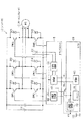
図1に、本実施形態にかかるモータジェネレータ10の制御システムの全体構成を示す。 FIG. 1 shows an overall configuration of a control system for a motor generator 10 according to the present embodiment.
図示されるように、モータジェネレータ10の3つの相(U相、V相、W相)には、インバータ12が接続されている。このインバータ12は、3相インバータであり、高圧バッテリ14の電圧をモータジェネレータ10の3つの相に適宜印加する。詳しくは、インバータ12は、3つの相のそれぞれと高圧バッテリ14の正極側又は負極側とを導通させるべく、スイッチング素子SW1、SW2とスイッチング素子SW3,SW4とスイッチング素子SW5,SW6との並列接続体を備えて構成されている。そして、スイッチング素子SW1及びスイッチング素子SW2を直列接続する接続点がモータジェネレータ10のU相と接続されている。また、スイッチング素子SW3及びスイッチング素子SW4を直列接続する接続点がモータジェネレータ10のV相と接続されている。更に、スイッチング素子SW5及びスイッチング素子SW6を直列接続する接続点がモータジェネレータ10のW相と接続されている。ちなみに、これらスイッチング素子SW1〜SW6は、本実施形態では、絶縁ゲートバイポーラトランジスタ(IGBT)によって構成されている。また、インバータ12は、各スイッチング素子SW1〜SW6に逆並列に接続されたフライホイールダイオードD1〜D6を備えている。
As shown in the figure, an
更に、インバータ12には、インバータ12の温度を検出する感温ダイオードDSが設けられている。
Further, the
上記スイッチング素子SW1〜SW6は、ドライバユニット16を介して、低圧バッテリ18を電力源とする電子制御装置(ECU20)により操作される。この際、ECU20では、ドライバユニット16を介して感温ダイオードDSの検出する温度を取り込み、同温度を上記操作に反映させる。 The switching elements SW1 to SW6 are operated via the driver unit 16 by an electronic control unit (ECU 20) using the low voltage battery 18 as a power source. At this time, the ECU 20 takes in the temperature detected by the temperature-sensitive diode DS via the driver unit 16 and reflects the temperature in the above operation.
図1には、ドライバユニット16やECU20のうち、感温ダイオードDSの検出する温度を取り込む処理の機能ブロックを示している。以下、これについて説明する。
FIG. 1 shows functional blocks of processing for taking in the temperature detected by the temperature-sensitive diode DS in the driver unit 16 and the
PWM変調部30は、感温ダイオードDSの出力するアナログ信号をパルス幅変調することで、論理「H」及び論理「L」からなる2値信号に変換する。送信部40は、PWM変調部30から出力される2値信号を、信号線SLを介してECU20側に出力するものである。定電圧生成部50は、低圧バッテリ18の電圧に基づき、所定の電圧値VH(例えば「15V」)の電圧を生成する。PWM変調部30及び送信部40は、定電圧生成部50を電力源する。
The
受信部60は、信号線SLを介して送信部40から送信された2値信号を受信する部分である。なお、送信部40及び受信部60間は、接地線GLによっても接続されている。マイコン70は、受信部60から信号を受信することで、スイッチング素子SW1〜SW6の操作態様を決定する。定電圧生成部72は、低圧バッテリ18の電圧VBを所定の電圧値VL(例えば「5V」)に変換する。受信部60やマイコン70は、定電圧生成部72を電力源とする。また、送信部40のうち出力部についても、定電圧生成部72を電力源とする。
The
図2に、感温ダイオードDSの検出値をマイコン70に送信する際の電気経路の詳細を示す。
FIG. 2 shows details of the electrical path when the detected value of the temperature sensitive diode DS is transmitted to the
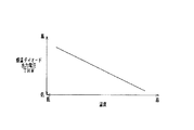
図示されるように、感温ダイオードDSは、上記定電圧生成部50と接続される定電流源52と接地との間に接続されている。そして、感温ダイオードDSと定電流源52との接続点を介して検出信号THWが出力される。図3に、検出対象の温度と検出信号THWとの関係を示す。図示されるように、温度が高いほど検出信号THWは小さい値となる。
As shown in the figure, the temperature-sensitive diode DS is connected between a constant
検出信号THWは、先の図2に示すPWM変調部30のコンパレータ32の非反転入力端子に取り込まれる。一方、コンパレータ32の反転入力端子には、三角波発生回路34の出力する三角波形状のキャリア信号が印加される。これにより、コンパレータ32は、検出信号THWをパルス幅変調した2値信号SP1を出力する。図4に、検出信号THWと2値信号SP1とを示す。詳しくは、図4(a1)に検出信号THWを示し、図4(b1)に2値信号SP1を示す。同様に、図4(a2)にも検出信号THWを示し、図4(b2)にも2値信号SP1を示す。図4(a2)及び図4(b2)に示す例では、検出信号THWがキャリアの最低値αと一致する例を示している。このように、検出信号THWが最低値α以下となるときには、2値信号SP1は、論理「L」が継続する信号となる。換言すれば、感温ダイオードDSの検出する温度が所定以上となるときには、2値信号SP1は、論理「L」が継続する信号となる。
The detection signal THW is taken into the non-inverting input terminal of the
2値信号SP1は、先の図2に示す送信部40に入力される。送信部40は、フォトカプラ41を備えている。フォトカプラ41の発光ダイオードのカソード側は接地されており、アノード側は抵抗体43,42を介して、定電圧生成部50の出力端子に接続されている。そして、抵抗体42及び抵抗体43の接続点が、コンパレータ32の出力端子と接続されている。
The binary signal SP1 is input to the
フォトカプラ41のフォトトランジスタのコレクタ側は、抵抗値R3の抵抗体44を介して、定電圧生成部72の出力端子に接続されている。より正確には、抵抗体44及び先の図1に示す給電線PLを介して、定電圧生成部72の出力端子に接続されている。また、フォトカプラ41のフォトトランジスタのエミッタは、接地されている。詳しくは、フォトカプラ41のフォトトランジスタのエミッタは、接地線GLと接続されている。
The collector side of the phototransistor of the
フォトカプラ41のコレクタは、信号線SLを介して、受信部60と接続されている。受信部60においては、信号線SLとの接点が、抵抗値R2の抵抗体61を介して定電圧生成部72の出力端子と接続されている。また、信号線SLとの接点は、抵抗値R1の抵抗体62を介して接地されている。詳しくは、抵抗体62を介して接地線GLと接続されている。
The collector of the
電圧変換回路63は、受信部60と信号線SLとの接点の電位(電圧信号SP2)の周波数を、アナログ電圧値に変換する。マイコン70は、電圧変換回路63の出力するアナログ信号を、ディジタルデータに変換し、ディジタル演算を行う。
The
上記構成によれば、感温ダイオードDSによって検出される温度情報を高精度に伝送することが可能となる。これは以下の理由による。 According to the above configuration, temperature information detected by the temperature-sensitive diode DS can be transmitted with high accuracy. This is due to the following reason.
一般に、基板上の配線よりも基板間を接続する電線(信号線SL)の方がノイズの影響を受けやすい。しかし、ドライバユニット16が高電圧制御システムを構成するものであるのに対し、ECU20が低圧制御システムを構成するものであるため、これらは別の基板に形成される傾向にある。このため、これらの間で通信を行う場合、電線を用いるのが一般的であり、この場合、ノイズの影響を受けやすくなる。更に、フォトカプラ41は、アナログ信号入力に応じたアナログ信号を出力することができるとはいえ、入力信号を出力信号に変換する際には誤差が生じやすい。このため、フォトカプラ41を介してアナログ信号を出力する場合、アナログ信号の値を高精度に伝送することが困難となる。
In general, an electric wire (signal line SL) connecting between substrates is more susceptible to noise than wiring on the substrate. However, since the driver unit 16 constitutes a high voltage control system, whereas the
この点、本実施形態では、PWM変調部30によって感温ダイオードDSの検出信号THWを2値信号に変換した。このため、信号線SLを伝播する信号の電圧レベルは、論理「H」レベル及び論理「L」レベルの2つの電圧レベルとなるため、ノイズの影響を受けにくい。また、フォトカプラ41を介して出力される信号を2値信号とすることができるため、フォトカプラ41の出力信号レベルの誤差は問題とならない。このように、本実施形態によれば、アナログ信号である検出信号THWを2値信号に変換してこれを伝送することで、感温ダイオードDSによって検出される温度情報を高精度に伝送することができる。
In this regard, in the present embodiment, the
更に、上記構成によれば、信号線SLが断線した際に、これを適切に検出することもできる。すなわち、本実施形態では、信号線SLが断線していないときにおいて、フォトカプラ41がオン状態であるときには、電圧変換回路63が取り込む電位は、接地電位レベル(論理「L」レベル)となり、フォトカプラ41がオフ状態であるときには、信号線SLの電位は、抵抗体44及び抵抗体61,62による分圧値「R1×VL/[R2R3/{(R2+R3)+R1}]:論理「H」レベル)となる。これに対し、信号線SLが断線したときには、電圧変換回路63が取り込む電位は、抵抗体61及び抵抗体62による分圧値「R1×VL/(R1+R2)」となる。このため、電圧変換回路63では、図5に示すように、電圧信号SP2の電圧レベルが2値信号の電圧レベルの中間の電圧レベルとなるときに、信号線SLが断線していると判断することができる。
Furthermore, according to the above configuration, when the signal line SL is disconnected, it can be appropriately detected. In other words, in the present embodiment, when the signal line SL is not disconnected and the
詳しくは、本実施形態では、図5に示すように、上記抵抗体44,61,62の抵抗値R1〜R3は、電圧変換回路63が断線時に取り込む電圧レベルが、2値信号の2つの電圧レベルの略中央となるように設定する。これにより、ノイズ等の影響や電圧変換回路63による電圧レベルの判定誤差等の影響にかかわらず、これら3つの電圧レベルを適切に識別することができる。特に断線時の電圧レベルを、2値信号の2つの電圧レベルの中間とすることで、2値信号の電圧レベルを、使用可能な電圧領域を十分活用して設定することができる。これにより、2値信号の2つの電圧レベルを十分に離間させることができ、ひいてはノイズの影響を好適に抑制することができる。しかも、信号線SLの断線時には、2値信号の電圧レベルの中間の電圧レベルにおいて固定した値となるため、ノイズ等の影響によらず断線を検出することができる。これに対し、断線時の電圧レベルを2値信号の電圧レベルよりも高くするかあるいは低くする場合には、使用可能な電圧領域のうち断線用の電圧レベルの分を除いた残りの領域で2値信号の2つの電圧レベルを設定する必要が生じる。この場合、2値信号の2つの電圧レベルが近似したものとなりやすく、ノイズ等の影響を受けやすくなるため、2値信号の検出精度が低下する。
Specifically, in the present embodiment, as shown in FIG. 5, the resistance values R1 to R3 of the
なお、例えば受信部60と信号線SLとの接点を抵抗体61を介して定電圧生成部72と接続することをやめる場合、信号線SLの断線時には、上記接点は接地電位レベルとなる。これは、2値信号の論理「L」レベルが継続する状態と等しくなるため、感温ダイオードDSの検出する温度が所定以上であることと対応している。このため、断線の検出を適切に行うことができない。このように、検出信号THWがPWM変調部30のキャリアの上限及び下限間の全領域を取り得る場合には、断線時の電圧レベルを2値信号の電圧レベルと一致させると断線を検出することができなくなる。
For example, when the contact between the receiving
以上詳述した本実施形態によれば、以下の効果が得られるようになる。 According to the embodiment described in detail above, the following effects can be obtained.
(1)信号線SLが断線するとき、受信部60と信号線SLとの接点の電位が、2値信号の2つの電圧レベルの中間の電圧レベルとなるように設定した。これにより、2値信号の2つの電圧レベルを設定するに際し、使用可能な電圧領域を極力有効活用しつつも、断線を適切に検出することもできる。
(1) When the signal line SL is disconnected, the potential at the contact point between the receiving
(2)受信部60を、信号線SLとの接点と定電圧生成部72の出力端子とを接続する抵抗体61を備えて構成するとともに、送信部40を、定電圧生成部72及び接地間に直列接続された抵抗体44及びフォトカプラ41を備えて構成した。これにより、抵抗体44や抵抗体61によって、受信部60の受信する電圧信号SP2の電圧レベル(2値信号の電圧レベル)を設定することができる。
(2) The receiving
(3)受信部60を、信号線SLとの接点と定電圧生成部72の出力端子とを接続する抵抗体61に加えて、信号線SLとの接点及び接地を接続する抵抗体62を備えて構成した。これにより、信号線SLが断線した際の受信部60の受信する電圧を、抵抗体61、62による定電圧生成部72の出力電圧の分圧値とすることができる。
(3) In addition to the
(4)フォトカプラ41を接地側に接続して且つ、フォトカプラ41及び抵抗体44間に信号線SLを接続した。これにより、フォトカプラ41がオン状態であるときの信号線SLの電圧レベルを、接地の電圧レベルとすることができる。
(4) The
(5)感温ダイオードDSの検出信号THWをパルス幅変調するPWM変調部30を備えた。これにより、出力信号の送信に際してのノイズに対する耐性を向上させることができる。
(5) The
(6)車載モータジェネレータ10を駆動するための高圧制御システムから高圧制御システムに指令を出す低圧制御システムへとアナログ信号を送信するために、送信部40及び受信部60を設けた。これら高圧制御システム及び低圧制御システム間の通信に際しては、特にノイズの影響を受けやすい傾向にある。このため、PWM変調部30を備えることが特に有効である。
(6) The
(第2の実施形態)
以下、第2の実施形態について、先の第1の実施形態との相違点を中心に図面を参照しつつ説明する。
(Second Embodiment)
Hereinafter, the second embodiment will be described with reference to the drawings with a focus on differences from the first embodiment.
図6に、本実施形態にかかる送信部40及び受信部60の構成を示す。なお、図6において、先の図2に示した部材に対応する部材については便宜上同一の符号を付している。
FIG. 6 shows configurations of the
図示されるように、本実施形態では、送信部40において、定電圧生成部72の出力端子側にフォトカプラ41を接続し、接地側に抵抗体44を接続する。図7にこの場合の、受信部60と信号線SLとの接点の電位(電圧信号SP2)を示す。本実施形態では、2値信号のうち低電位側の値が「0」ではない。代わりに、2値信号のうち高電位側の値が、定電圧生成部72の出力する電圧値VLとなっている。なお、断線時の電圧レベルは、抵抗体44、61,62の抵抗値R4〜R6を調節することで、2値信号の2つの電圧レベルの略中央の値となるようにする。
As illustrated, in the present embodiment, in the
以上説明した本実施形態によれば、先の第1の実施形態の上記(1)〜(3)、(5)、(6)の効果を得ることができる。 According to this embodiment described above, the effects (1) to (3), (5), and (6) of the first embodiment can be obtained.
(第3の実施形態)
以下、第3の実施形態について、先の第1の実施形態との相違点を中心に図面を参照しつつ説明する。
(Third embodiment)
Hereinafter, the third embodiment will be described with reference to the drawings with a focus on differences from the first embodiment.
図8に、本実施形態にかかる送信部40及び受信部60の構成を示す。なお、図8において、先の図2に示した部材に対応する部材については便宜上同一の符号を付している。
FIG. 8 shows configurations of the
図8に示すように、本実施形態では、送信部40において、フォトカプラ41のフォトトランジスタのコレクタを、抵抗体44を介して定電圧生成部50の出力端子と接続する。また、受信部60において、抵抗体62に対応するものを備えない。換言すれば、受信部60と信号線SLとの接点は、抵抗体61を介して定電圧生成部72の出力端子と接続されるものの、接地されてはいない。
As shown in FIG. 8, in the present embodiment, in the
図9に、受信部60と信号線SLとの接点の電位(電圧信号SP2)を示す。なお、断線時の電圧信号SP2の電圧レベル(VL)を、2値信号の略中央とすべく、抵抗体44及び抵抗体61の抵抗値R7,R8を調節する。
FIG. 9 shows the potential (voltage signal SP2) at the contact point between the receiving
以上説明した本実施形態によれば、先の第1の実施形態の上記(1)、(2)、(4)〜(6)の効果を得ることができる。 According to the present embodiment described above, the effects (1), (2), (4) to (6) of the first embodiment can be obtained.
(第4の実施形態)
以下、第4の実施形態について、先の第3の実施形態との相違点を中心に図面を参照しつつ説明する。
(Fourth embodiment)
Hereinafter, the fourth embodiment will be described with reference to the drawings with a focus on differences from the third embodiment.
図10に、本実施形態にかかる送信部40及び受信部60の構成を示す。なお、図10において、先の図8に示した部材に対応する部材については便宜上同一の符号を付している。
FIG. 10 shows configurations of the
図示されるように、本実施形態では、接地側に抵抗体44を接続し、定電圧生成部50の出力端子側にフォトカプラ41を接続している。図11に、受信部60と信号線SLとの接点の電位(電圧信号SP2)を示す。なお、断線時の電圧信号SP2の電圧レベル(VL)を、2値信号の略中央とすべく、抵抗体44及び抵抗体61の抵抗値を調節する。
As shown in the figure, in the present embodiment, a
以上説明した本実施形態によれば、先の第1の実施形態の上記(1)、(2)、(5)、(6)の効果を得ることができる。 According to the present embodiment described above, the effects (1), (2), (5), and (6) of the previous first embodiment can be obtained.
(その他の実施形態)
なお、上記各実施形態は、以下のように変更して実施してもよい。
(Other embodiments)
Each of the above embodiments may be modified as follows.
・送信部40及び受信部60の電源としては、上記各実施形態で例示したものに限らない。例えば図2において、フォトカプラ41のフォトトランジスタのコレクタを抵抗体44を介して定電圧生成部50の出力端子や、バッテリ14の正極端子と接続してもよい。この際、受信部60と送信部40との電源電圧は同一でなくてもよい。
-The power supply of the
・モータジェネレータ10を駆動するための高圧制御システムとしては、インバータ12を備えるものに限らず、例えばインバータ12の高圧電力を生成するDC−DCコンバータを備えるものであってもよい。
The high voltage control system for driving the motor generator 10 is not limited to the one provided with the
・高圧制御システムと低圧制御システムとを絶縁しつつこれら双方間での通信を可能とする絶縁素子からなるスイッチ手段としては、フォトカプラに限らない。例えばフォトMOSリレーであってもよい。 The switch means composed of an insulating element that enables communication between both of the high-pressure control system and the low-pressure control system is not limited to the photocoupler. For example, a photo MOS relay may be used.
・信号線SLとしては、高圧制御システムと低圧制御システムとを接続するものに限らない。異なる基板間の通信に供されるものであれば、ノイズの影響を受けやすいため、PWM変調部によって変調された信号を用いることが有効である。この際、PWM変調による上限及び下限間の全領域を、変換対象となるアナログ信号が包含する場合には、2値信号のいずれか一方の電位に固定されることを持って断線した旨を検出することはできないため、本発明は特に有効である。 The signal line SL is not limited to connecting the high voltage control system and the low voltage control system. Since it is easy to be affected by noise if it is used for communication between different substrates, it is effective to use a signal modulated by the PWM modulation section. At this time, if the analog signal to be converted includes the entire range between the upper limit and the lower limit by PWM modulation, it is detected that the wire is disconnected with being fixed to one of the potentials of the binary signal. The present invention is particularly effective because it cannot be done.
・送信を所望する信号としては、感温ダイオードDSの検出信号THWに限らない。例えば、信号線SLが高圧制御システムと低圧制御システムとを接続する場合、高圧制御システムの特定の物理量を検出する検出手段の出力信号としてよい。また、内燃機関のアクチュエータの操作信号であるデューティ信号(2値信号)であってもよい。この場合であっても、信号線の断線を検出するために本発明の適用は有効である。ただし、この場合、アクチュエータ側が受信部となるため、断線時に別の信号線を介してその旨を伝えることが望ましい。 The signal desired to be transmitted is not limited to the detection signal THW of the temperature-sensitive diode DS. For example, when the signal line SL connects a high-pressure control system and a low-pressure control system, the signal line SL may be an output signal of a detection unit that detects a specific physical quantity of the high-pressure control system. Further, it may be a duty signal (binary signal) that is an operation signal of the actuator of the internal combustion engine. Even in this case, the application of the present invention is effective for detecting the disconnection of the signal line. However, in this case, since the actuator side serves as a receiving unit, it is desirable to notify that via a separate signal line at the time of disconnection.
・信号線が断線するとき、受信部60と信号線SLとの接点の電位が2値信号の2つの電圧レベルの中間の電圧レベルとなるような設定手法としては、上記各実施形態で例示したものに限らない。例えば図8に示す構成において、送信部40の出力段を、電源及び接地間に接続されるCMOS回路としてもよい。この場合、電源と接続されるトランジスタが導通状態とされることで、論理「H」レベルの信号が出力され、接地されるトランジスタが導通状態とされることで、論理「L」レベルの信号が出力される。そして、受信部60と信号線SLとの接点と接続される電源の電圧を、CMOS回路に接続される電源の電圧よりも低くしておくなら、信号線SLの断線時において、受信部60と信号線SLとの接点の電位を2値信号の2つの電圧レベルの中間の電圧レベルとすることができる。
The setting method in which the potential of the contact point between the receiving
10…モータジェネレータ、12…インバータ、16…ドライバユニット、20…ECU、30…PWM変調部、40…送信部、60…受信部。 DESCRIPTION OF SYMBOLS 10 ... Motor generator, 12 ... Inverter, 16 ... Driver unit, 20 ... ECU, 30 ... PWM modulation part, 40 ... Transmission part, 60 ... Reception part.
Claims (7)
前記信号線を介して前記2値信号を送信する送信手段と、
前記信号線を介して前記2値信号を受信する受信手段とを備え、
前記送信手段が、電源及び接地間に直列接続された抵抗体及びスイッチ手段を備えて且つ、該抵抗体及びスイッチ手段の接続点に前記信号線を接続するとともに、前記受信手段が、前記信号線との接点及び前記接地を接続する第1の抵抗体と、電源及び前記接点間を接続する第2の抵抗体とを備えることで、前記信号線が断線するとき、前記受信手段と前記信号線との接点の電位が、前記2値信号の2つの電圧レベルの中間の電圧レベルとなるように設定されてなることを特徴とする断線検出装置。 In a disconnection detecting device for detecting the presence or absence of disconnection of a signal line for propagating a binary signal in a control system of an in-vehicle motor,
Transmitting means for transmitting the binary signal via the signal line;
Receiving means for receiving the binary signal via the signal line ,
The transmitter includes a resistor and a switch connected in series between a power source and a ground, and connects the signal line to a connection point of the resistor and the switch, and the receiver includes the signal line. When the signal line is disconnected, the receiving means and the signal line are provided with a first resistor that connects the contact point and the ground, and a second resistor that connects the power source and the contact point. The disconnection detecting device is characterized in that the potential of the contact with the voltage is set to a voltage level intermediate between the two voltage levels of the binary signal.
前記スイッチ手段は、前記接地側に接続されることを特徴とする請求項1記載の断線検出装置。 The disconnection detecting device according to claim 1, wherein the switch means is connected to the ground side.
前記送信手段は、前記車載電動機を駆動するための高圧制御システム、及び該高圧制御システムに指令を出す低圧制御システムの少なくとも一方から他方へとアナログ信号を送信するための手段であり、
前記受信手段は、前記他方において、前記送信される信号を受信する手段であることを特徴とする請求項4記載の断線検出装置。 The control system is a control system for an in-vehicle motor,
The transmission means is means for transmitting an analog signal from at least one of a high-pressure control system for driving the vehicle-mounted electric motor and a low-pressure control system that issues a command to the high-pressure control system,
5. The disconnection detecting device according to claim 4 , wherein the receiving means is means for receiving the transmitted signal on the other side.
前記検出手段としての感温ダイオードと、
前記感温ダイオードによる温度の検出対象となるインバータとを備えることを特徴とする制御システム。 A disconnection detecting device according to claim 6 ;
A temperature sensitive diode as the detecting means;
A control system comprising: an inverter that is a temperature detection target of the temperature sensitive diode .
Priority Applications (1)
| Application Number | Priority Date | Filing Date | Title |
|---|---|---|---|
| JP2007104467A JP4816552B2 (en) | 2007-04-12 | 2007-04-12 | Disconnection detection device and control system |
Applications Claiming Priority (1)
| Application Number | Priority Date | Filing Date | Title |
|---|---|---|---|
| JP2007104467A JP4816552B2 (en) | 2007-04-12 | 2007-04-12 | Disconnection detection device and control system |
Publications (2)
| Publication Number | Publication Date |
|---|---|
| JP2008261719A JP2008261719A (en) | 2008-10-30 |
| JP4816552B2 true JP4816552B2 (en) | 2011-11-16 |
Family
ID=39984308
Family Applications (1)
| Application Number | Title | Priority Date | Filing Date |
|---|---|---|---|
| JP2007104467A Expired - Fee Related JP4816552B2 (en) | 2007-04-12 | 2007-04-12 | Disconnection detection device and control system |
Country Status (1)
| Country | Link |
|---|---|
| JP (1) | JP4816552B2 (en) |
Families Citing this family (2)
| Publication number | Priority date | Publication date | Assignee | Title |
|---|---|---|---|---|
| KR101312263B1 (en) * | 2012-03-23 | 2013-09-25 | 삼성에스디아이 주식회사 | Vehicle and method for controlling the same |
| JP7771879B2 (en) * | 2022-06-30 | 2025-11-18 | 株式会社デンソー | Disconnection detection method and disconnection detection circuit |
Family Cites Families (4)
| Publication number | Priority date | Publication date | Assignee | Title |
|---|---|---|---|---|
| JP2633619B2 (en) * | 1988-05-10 | 1997-07-23 | ファナック株式会社 | Encoder disconnection detection circuit |
| JPH01302180A (en) * | 1988-05-31 | 1989-12-06 | Hitachi Seiko Ltd | Disconnection detecting system |
| JPH0694772A (en) * | 1992-09-10 | 1994-04-08 | Nippondenso Co Ltd | Binary signal detection circuit having abnormality detecting function |
| JPH09172781A (en) * | 1995-12-15 | 1997-06-30 | Denso Corp | Motor control device for electric vehicle driving |
-
2007
- 2007-04-12 JP JP2007104467A patent/JP4816552B2/en not_active Expired - Fee Related
Also Published As
| Publication number | Publication date |
|---|---|
| JP2008261719A (en) | 2008-10-30 |
Similar Documents
| Publication | Publication Date | Title |
|---|---|---|
| US7071698B2 (en) | Power supply apparatus for detecting battery voltage and the portions of faults | |
| US10862537B2 (en) | Power line communication device, in-vehicle device and in-vehicle system | |
| CN111902725B (en) | Sensor devices for vehicles | |
| JP5092762B2 (en) | In-vehicle information transmission device | |
| CN111213312A (en) | Inverter control board | |
| JP2009136115A (en) | Signal transmission device | |
| JP5359604B2 (en) | Control device for power conversion circuit | |
| CN104659745A (en) | Vehicle motor drive circuit | |
| US20190348980A1 (en) | Suppressing circuit for semiconductor switch | |
| JP4816552B2 (en) | Disconnection detection device and control system | |
| CN108475998B (en) | Control system of power conversion device | |
| JP5776636B2 (en) | Temperature detection device | |
| US20220278524A1 (en) | Power supply system with protection against current variations | |
| EP4528953A1 (en) | Electronic control device and electronic control method | |
| JP5202119B2 (en) | Multi-output judgment circuit | |
| CN116080448A (en) | Control unit for electric vehicle | |
| US20210167717A1 (en) | Motor drive system with correction function of temperature deviation of igbt module | |
| JP2010035284A (en) | Overcurrent protection circuit | |
| CN111886504B (en) | sensor components for vehicles | |
| WO2017099191A1 (en) | Signal transfer circuit | |
| JP5119890B2 (en) | In-vehicle control system abnormality detection device and in-vehicle control system | |
| JP7552554B2 (en) | Switch drive device and program | |
| US11325478B2 (en) | Control apparatus, vehicle system, and control method | |
| US20260035031A1 (en) | Motor-driven power steering device, method for controlling the same, and vehicle having the same | |
| KR100456848B1 (en) | Intelligent power module apparatus of electric vehicle |
Legal Events
| Date | Code | Title | Description |
|---|---|---|---|
| A621 | Written request for application examination |
Free format text: JAPANESE INTERMEDIATE CODE: A621 Effective date: 20090605 |
|
| A977 | Report on retrieval |
Free format text: JAPANESE INTERMEDIATE CODE: A971007 Effective date: 20110512 |
|
| A131 | Notification of reasons for refusal |
Free format text: JAPANESE INTERMEDIATE CODE: A131 Effective date: 20110517 |
|
| A521 | Request for written amendment filed |
Free format text: JAPANESE INTERMEDIATE CODE: A523 Effective date: 20110714 |
|
| TRDD | Decision of grant or rejection written | ||
| A01 | Written decision to grant a patent or to grant a registration (utility model) |
Free format text: JAPANESE INTERMEDIATE CODE: A01 Effective date: 20110802 |
|
| A01 | Written decision to grant a patent or to grant a registration (utility model) |
Free format text: JAPANESE INTERMEDIATE CODE: A01 |
|
| A61 | First payment of annual fees (during grant procedure) |
Free format text: JAPANESE INTERMEDIATE CODE: A61 Effective date: 20110815 |
|
| FPAY | Renewal fee payment (event date is renewal date of database) |
Free format text: PAYMENT UNTIL: 20140909 Year of fee payment: 3 |
|
| R151 | Written notification of patent or utility model registration |
Ref document number: 4816552 Country of ref document: JP Free format text: JAPANESE INTERMEDIATE CODE: R151 |
|
| FPAY | Renewal fee payment (event date is renewal date of database) |
Free format text: PAYMENT UNTIL: 20140909 Year of fee payment: 3 |
|
| R250 | Receipt of annual fees |
Free format text: JAPANESE INTERMEDIATE CODE: R250 |
|
| R250 | Receipt of annual fees |
Free format text: JAPANESE INTERMEDIATE CODE: R250 |
|
| R250 | Receipt of annual fees |
Free format text: JAPANESE INTERMEDIATE CODE: R250 |
|
| R250 | Receipt of annual fees |
Free format text: JAPANESE INTERMEDIATE CODE: R250 |
|
| R250 | Receipt of annual fees |
Free format text: JAPANESE INTERMEDIATE CODE: R250 |
|
| R250 | Receipt of annual fees |
Free format text: JAPANESE INTERMEDIATE CODE: R250 |
|
| R250 | Receipt of annual fees |
Free format text: JAPANESE INTERMEDIATE CODE: R250 |
|
| R250 | Receipt of annual fees |
Free format text: JAPANESE INTERMEDIATE CODE: R250 |
|
| R250 | Receipt of annual fees |
Free format text: JAPANESE INTERMEDIATE CODE: R250 |
|
| LAPS | Cancellation because of no payment of annual fees |