JP4814791B2 - Level shifter - Google Patents
Level shifter Download PDFInfo
- Publication number
- JP4814791B2 JP4814791B2 JP2006526065A JP2006526065A JP4814791B2 JP 4814791 B2 JP4814791 B2 JP 4814791B2 JP 2006526065 A JP2006526065 A JP 2006526065A JP 2006526065 A JP2006526065 A JP 2006526065A JP 4814791 B2 JP4814791 B2 JP 4814791B2
- Authority
- JP
- Japan
- Prior art keywords
- signal
- voltage domain
- terminal
- signal terminal
- transistor
- Prior art date
- Legal status (The legal status is an assumption and is not a legal conclusion. Google has not performed a legal analysis and makes no representation as to the accuracy of the status listed.)
- Expired - Lifetime
Links
- 230000002457 bidirectional effect Effects 0.000 claims description 12
- 230000000903 blocking effect Effects 0.000 claims description 7
- 230000004044 response Effects 0.000 claims description 7
- 238000000034 method Methods 0.000 claims description 3
- 230000009977 dual effect Effects 0.000 claims 1
- 102100036285 25-hydroxyvitamin D-1 alpha hydroxylase, mitochondrial Human genes 0.000 description 28
- 101000875403 Homo sapiens 25-hydroxyvitamin D-1 alpha hydroxylase, mitochondrial Proteins 0.000 description 28
- 230000008859 change Effects 0.000 description 16
- 238000010586 diagram Methods 0.000 description 9
- 230000008901 benefit Effects 0.000 description 3
- 238000012986 modification Methods 0.000 description 3
- 230000004048 modification Effects 0.000 description 3
- 238000013459 approach Methods 0.000 description 2
- 239000000872 buffer Substances 0.000 description 2
- 230000005669 field effect Effects 0.000 description 2
- 230000008878 coupling Effects 0.000 description 1
- 238000010168 coupling process Methods 0.000 description 1
- 238000005859 coupling reaction Methods 0.000 description 1
- 238000005516 engineering process Methods 0.000 description 1
- 230000006872 improvement Effects 0.000 description 1
- 230000002093 peripheral effect Effects 0.000 description 1
Images


Classifications
-
- H—ELECTRICITY
- H03—ELECTRONIC CIRCUITRY
- H03K—PULSE TECHNIQUE
- H03K19/00—Logic circuits, i.e. having at least two inputs acting on one output; Inverting circuits
- H03K19/0175—Coupling arrangements; Interface arrangements
- H03K19/0185—Coupling arrangements; Interface arrangements using field effect transistors only
-
- H—ELECTRICITY
- H03—ELECTRONIC CIRCUITRY
- H03K—PULSE TECHNIQUE
- H03K3/00—Circuits for generating electric pulses; Monostable, bistable or multistable circuits
- H03K3/02—Generators characterised by the type of circuit or by the means used for producing pulses
- H03K3/353—Generators characterised by the type of circuit or by the means used for producing pulses by the use, as active elements, of field-effect transistors with internal or external positive feedback
- H03K3/356—Bistable circuits
- H03K3/356104—Bistable circuits using complementary field-effect transistors
- H03K3/356113—Bistable circuits using complementary field-effect transistors using additional transistors in the input circuit
Landscapes
- Engineering & Computer Science (AREA)
- Computer Hardware Design (AREA)
- Physics & Mathematics (AREA)
- Computing Systems (AREA)
- General Engineering & Computer Science (AREA)
- Mathematical Physics (AREA)
- Logic Circuits (AREA)
Description
[発明の背景]
[発明の分野]
本発明は、一般的に集積回路に関し、特に、集積回路用のレベル・シフターに関する。
[Background of the invention]
[Field of the Invention]
The present invention relates generally to integrated circuits, and more particularly to level shifters for integrated circuits.
[関連技術の説明]
レベル・シフターは、信号の電圧を第1の電圧から第2の電圧へ変えるため集積回路で利用されている。
[Description of related technology]
Level shifters are used in integrated circuits to change the voltage of a signal from a first voltage to a second voltage.
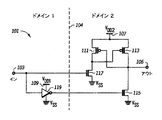
図1は、従来技術のレベル・シフターの回路図である。レベル・シフター101は、集積回路の電圧ドメイン1(ドメイン1)に配置された回路と、集積回路の電圧ドメイン2(ドメイン2)に配置された回路とを含む。電圧ドメインは、所与の供給電圧で動作可能である集積回路の部分である。インバータ119は、ドメイン1に配置されている。N型電界効果トランジスタ(NFET)117及び115とP型電界効果トランジスタ(PFET)111及び113とが、ドメイン1に配置されている。インバータ119は、ドメイン1の電圧供給線109(VDD1である)に結合された電源端子を含む。PFET111のソース/ドレーン端子(FETの電流端子)及びPFET113のソース/ドレーン端子は、ドメイン2の電圧供給線107(VDD2である)に接続されている。
FIG. 1 is a circuit diagram of a prior art level shifter. The
入力端子103の高電圧(例えば、VDD1)は、NFET117を導通させ、そしてインバータ119の出力をVSSに引く。インバータ119の出力がVSSになることにより、NFET115は非導通になる。NFET117を導通にすることにより、PFET113のゲート端子(FETの制御端子)はVSSに引かれ、PFET113を導通にする。PFET113を導通にすることにより、出力端子105がVDD2に引かれ、それによりPFET111を非導通にする。従って、入力端子103におけるVDD1の高電圧への変化は、出力端子105におけるVDD2の高電圧への変化に対応する。また、入力端子103におけるVSSの低電圧への変化は、出力端子105におけるVSSの低電圧への変化に対応する。
A high voltage (eg, VDD1) at
レベル・シフター101は、出力端子105の電圧が入力端子103の電圧の対応する変化を生じさせない点で一方向性である。その上、レベル・シフター101は、ドメイン境界104を横切る2つの線(インバータ119の出力からNFET115への線と、入力端子103からNFET117のゲート端子への線)を含む。
The
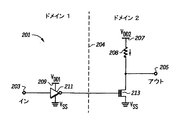
図2は、別の従来技術のレベル・シフターの回路図である。レベル・シフター201は、ドメイン2の電圧供給線207(VDD2である)に結合された抵抗208を含む。抵抗208は、NFET213に接続され、これら両方の構成要素は、第2の電圧ドメイン(ドメイン2)に配置されている。出力端子205は、NFET213のソース/ドレーン端子に接続されている。入力端子203は、インバータ211の入力に接続され、当該インバータ211は、電圧ドメイン1(ドメイン1)に配置されている。インバータ211の出力は、NFET213のゲート端子に結合されている。レベル・シフターは、ドメイン境界204を横切る単一の信号線(インバータ211の出力からNFET213のゲート端子への信号線)のみを有する。しかしながら、NFET213が導通状態であるとき、一定の電流が、抵抗208を流れる。この一定電流の流れは、動作中にエネルギを消費する。
FIG. 2 is a circuit diagram of another prior art level shifter.
必要とされることは、レベル・シフターの改良である。 What is needed is a level shifter improvement.
本発明が、より一層理解され得て、そしてその多くの目的、特徴及び利点が、添付図面を参照することにより当業者に対して明らかにされるであろう。 The invention may be better understood and its many objects, features and advantages will become apparent to those skilled in the art by reference to the accompanying drawings.
異なる図面での同じ参照番号の使用は、特記しない限り同じ構成要素を示す。 The use of the same reference numbers in different drawings indicates the same component unless otherwise indicated.
[詳細な説明]
以下は、本発明を実行するためのモードの詳細な説明を記載する。この詳細な説明は、本発明の例示であることを意図し、限定であるとるべきでない。
[Detailed description]
The following provides a detailed description of the modes for carrying out the present invention. This detailed description is intended to be illustrative of the invention and should not be taken as limiting.
図3は、本発明に従ったレベル・シフター301を含む集積回路300の一実施形態の回路図である。レベル・シフター301は、電圧ドメイン1(ドメイン1)に配置されたPFET321及び323とNFET325及び317とを含む。レベル・シフター301はまた、電圧ドメイン2(ドメイン2)に配置されたPFET311及び313とNFET327及び315とを含む。PFET321及び323のソース/ドレーン端子とNFET325のゲート端子とは、ドメイン1の電圧供給線309(VDD1である)に接続され、そしてNFET317のソース/ドレーン端子は、VSS線(電圧VSSである)に接続されている。
FIG. 3 is a circuit diagram of one embodiment of an integrated
PFET311及び313のソース/ドレーン端子とNFET327のゲート端子とは、ドメイン2の電圧供給線307(VDD2である)に接続され、そしてNFET315のソース・ドレーン端子は、VSS線に接続されている。
The source / drain terminals of
レベル・シフター301は、ドメイン1に配置された集積回路300の回路331に結合された第1の信号端子(ST1)303を含む。回路331は、VDD1で給電される。信号は、信号端子303を介して回路331とレベル・シフター301との間で伝達される。レベル・シフター301は、集積回路300の回路341に結合された第2の信号端子(ST2)305を含み、当該回路341は、ドメイン2に配置され、そしてVDD2で給電される。信号は、信号端子305を介して回路341とレベル・シフター301との間で伝達される。一実施形態において、信号端子303及び305は、レベル・シフター301と回路331の間の信号線及びレベル・シフター301と回路341の間の信号線のそれぞれに位置する。
レベル・シフター301は、低電圧(例えば、VSS)から高電圧(例えば、VDD1)への信号端子303の電圧の変化が信号端子305における低電圧(例えば、VSS)から高電圧(例えば、VDD2)への対応の変化を生じさせ、且つ高電圧から低電圧への信号端子303の電圧の変化が高電圧から低電圧への信号端子305の電圧の対応の変化を生じさせる点で非反転型レベル・シフターである。しかしながら、他の実施形態において、レベル・シフター301は、信号端子303の電圧の或る一方向の変化(例えば、低から高)が信号端子305の電圧の対応するその反対方向の変化(例えば、高から低)を生じさせる点で反転型レベル・シフターになり得る。
In the
レベル・シフター301は、信号端子305の電圧の変化がまた信号端子303の電圧の対応の変化を生じさせる点で双方向レベル・シフターである。従って、信号端子303を入力として利用することができ且つ信号端子305を出力として利用することができ、又は信号端子305を入力として利用することができ且つ信号端子303を出力として利用することができる。
示された実施形態において、信号端子303は、回路331に結合され、そして信号端子305は、回路341に結合されている。示された実施形態において、回路331は、信号を信号端子303に与え、そして信号を信号端子303から受け取ることが可能である。また、示された実施形態において、回路341は、信号を信号端子305から受け取り、そして信号を信号端子305に与えることが可能である。一実施形態において、回路331は、プロセッサ(図示せず)を含み、そして回路341は、I/Oパッド(図示せず)を含む。別の実施形態において、回路331は、周辺回路又はプロセッサ回路(図示せず)を含み、そして回路341は、双方向バス(図示せず)を含む。
In the illustrated embodiment,
示された実施形態において、回路331及び341のそれぞれは、レベル・シフター301を通る信号の流れを検出する回路を含む。示された実施形態において、回路331は、3状態バッファ333及び335を含み、当該3状態バッファ333及び335は、イン/*アウト信号により反対方向に制御されて、回路331が信号を信号端子303に与えるか、又は信号を信号端子303から受け取るかのいずれかを決定する。回路341はまた、3状態バッファ343及び345を含み、当該3状態バッファ343及び345は、イン/*アウト信号により反対方向に制御されて、回路341が信号を信号端子305に与えるか、又は信号を信号端子305から受け取るかのいずれかを決定する。集積回路300の動作中に、レベル・シフター301を用いて、信号をイン/*アウト信号の状態に応じていずれかの方向にシフトし得る。他の実施形態は、レベル・シフター301を通る信号の流れの方向を決定するための他の回路及び/又は他のオペレーティング・プロトコルを含み得る。
In the illustrated embodiment, each of the
双方向レベル・シフターを用いることは、ドメイン境界(例えば、304)を横切る回路の信号線の数をより少なくする利点を与え、それは、経路設定の輻輳を低減し得る。また、双方向レベル・シフターを用いることは、集積回路の回路構成の縮小を可能にし得る。 Using a bi-directional level shifter offers the advantage of reducing the number of circuit lines across the domain boundary (eg, 304), which can reduce routing congestion. Also, the use of a bidirectional level shifter may allow the circuit configuration of the integrated circuit to be reduced.
示された実施形態において、レベル・シフター301を利用して、信号の電圧をいずれの方向、即ち、上方に又は下方にシフトさせることができる。例えば、信号端子303を入力として利用し、そして信号端子305を出力として利用するとき、レベル・シフター301は、VDD1がVDD2より大きい又は小さいいずれの場合も動作することができる。同様に、信号端子305を入力として利用し、そして信号端子303を出力として利用するとき、レベル・シフター301は、VDD1がVDD2より大きい又は小さいいずれか場合も動作することができる。示された実施形態において、PFET323を利用して、信号端子303をVDD1に引き、そしてPFET311を利用して、信号端子305をVDD2に引く。従って、レベル・シフター301は、ドメイン1とドメイン2との電源電圧が独立に可変であるシステムにおいて動作可能である。例えば、レベル・シフター301は、VDD1及び/又はVDD2が、ドメイン1及び/又はドメイン2の回路が低電力モードで動作するその動作中に低減される場合も用いることができる。
In the illustrated embodiment, the
低電圧(例えば、VSS)から高電圧(例えば、VDD1)への信号端子303の電圧の変化は、NFET315が導通になるようにさせ、それによりPFET311のゲート端子をVSSに引いて、PFET311を導通させる。PFET311が導通状態であることにより、信号端子305がVDD2に引かれ、そしてPFET313のゲート端子がVDD2に引かれる。また、信号端子303が高電圧に行くことが、PFET321を非導通になるようにさせる。PFET311が導通になることにより、NFET317のゲート端子がVDD2に引かれ、それによりそのNFET317を導通状態にさせ、そしてPFET323のゲート端子をVSSに引き(、それがPFET323を導通状態にさせる)。PFET323を導通状態にさせることにより、信号端子303が、導通のPFET323を介してVDD1に引かれる。
A change in the voltage at the
レベル・シフター301はまた、信号端子303から信号端子305への電流経路を含み、当該電流経路は、NFET325及び327を含む。信号端子303が初めに低電圧(例えば、VSS)であるとき、NFET325及び327は、導通していて、信号端子305の電圧を信号端子303の低電圧(例えば、VSS)に引く。信号端子303の電圧が高電圧に変わるとき、信号端子305の電圧は、導通状態のNFET325及び327を通って信号端子303の電圧に向かって引かれる。NFET325及び327を通るこの経路は、信号端子303における電圧の変化から信号端子305における電圧の変化までの伝搬遅延を低減する利点を与える(そして逆も同様である)。
VDD1がVDD2より低い場合、信号端子303の電圧がVDD1に向かって上昇するので、ノード328の電圧が、NFET325の制御ゲートの電圧(VDD1)の(NFET325の)電圧スレッショルド内にある電圧に達する。NFET325がこの時点で非導通になるとき、NFET325及び327を流れる電流は、停止する。しかしながら、この時点で、PFET311は、導通状態であり、信号端子305の電圧をVDD2に「ロック」する。信号端子303が高電圧であり且つ信号端子305が高電圧であるとき、PFET323及び311が導通状態であるので、NFET325及び327が導通状態になることが、電圧供給線309及び307を互いに結合するようにさせる。しかしながら、上記で説明したように、信号端子303の電圧がVDD1に近づくので、NFET325が非導通になることが、VDD2線307とVDD1線309との間の経路の電流の流れを遮断する。
When VDD1 is lower than VDD2, the voltage at
VDD1がVDD2より高い場合、信号端子305の電圧がVSSからVDD2に向けて引かれるので、ノード330の電圧は、NFET327の制御ゲートの電圧(VDD2)の(NFET327の)電圧スレッショルド内にある電圧に近づき、それによりNFET327を非導通になるようにさせ、そしてVDD1線309からVDD2線307への経路の電流の流れを遮断する。
When VDD1 is higher than VDD2, the voltage at the
信号端子303の電圧が高電圧(例えば、VDD1)から低電圧(例えば、VSS)に行くとき、ノード328の電圧は、VDD1からNFET325のスレッショルド電圧より小さい電圧へ降下し、それによりNFET325が導通状態になり、ノード326を低に引き(、そしてNFET327を導通状態になるようにさせる)。NFET325及び327が導通状態になる場合、信号端子305は、そしてNFET327及び325を介して低電圧に引かれ、そして信号端子303はVSSに引かれる。
When the voltage at
信号端子303の電圧が高電圧から低電圧に行くことがまた、NFET315を非導通状態に、そしてPFET321を導通状態にさせる。信号端子305の電圧は、高電圧から低電圧に行くことが、PFET321を導通状態に、そしてNFET317を非導通状態にさせる。PFET313が導通状態になることが、PFET311を非導通状態にさせる。PFET321を導通状態にさせることは、PFET323を非導通状態にさせる。
The voltage at
レベル・シフター301は、信号端子305を入力として利用し、そして信号端子303を出力として利用するとき、同様の要領で動作し、そして上記で説明したように、PFET311及び313とNFET327及び315とは、信号端子303を入力として利用しそして信号端子305を出力として利用するとき、PFET323及び321とNFET325及び317と同様にそれぞれ動作し(、そしてその逆の場合も同様に動作する)。
図4は、本発明に従ったレベル・シフター401を含む集積回路400の別の実施形態を示す。レベル・シフター401は、集積回路400の電圧ドメイン1(ドメイン1)に配置されたPFET421及び423とNFET425及び417とを含む。レベル・シフター401はまた、集積回路400の電圧ドメイン2(ドメイン2)に配置されたPFET411及び413とNFET427及び415とを含む。PFET421及び423のソース/ドレーン端子とNFET425のゲート端子とは、ドメイン1の電圧供給線409(VDD1である)に接続され、そしてNFET417のソース/ドレーン端子は、VSS線に接続されている。PFET411及び413のソース/ドレーン端子とNFET427のゲート端子とは、ドメイン2の電圧供給線407(VDD2である)に接続され、そしてNFET415のソース/ドレーン端子は、VSS線に接続されている。
FIG. 4 illustrates another embodiment of an
レベル・シフター401は、ドメイン1に配置された集積回路400の回路431に結合されている第1の信号端子(ST1)403を含む。回路431は、図3の回路331に類似している。回路431は、VDD1で給電される。信号は、信号端子403を介して回路431とレベル・シフター401の間で伝達される。レベル・シフター401は、集積回路400の回路441に結合されている第2の信号端子(ST2)405を含み、当該回路441は、ドメイン2に配置され、そしてVDD2で給電される。回路441は、図3の回路341に類似している。信号は、信号端子405を介して回路441とレベル・シフター401との間で伝達される。
図3のレベル・シフター301の場合のように、レベル・シフター401は、双方向レベル・シフターであり、そこにおいて、信号端子403が入力として動作可能であり且つ信号端子405が出力として動作可能であり、又は信号端子405が入力として動作可能であり且つ信号端子403が出力として動作可能である。更に、レベル・シフター301の場合のように、レベル・シフター401は、VDD1がVDD2より大きい又は小さいいずれの場合もいずれの方向にも動作可能である。
As in the
レベル・シフター401は、信号端子403と信号端子405との間の電流経路を含み、当該電流経路は、NFET425及び427を含む。図3のNFET325及び327の場合のように、これらのNFETを利用して、信号端子403及び405が高電圧であるとき、(導通しているPFET423及び411を介した)VDD1線409とVDD2線407との間の電流の流れを遮断する。
レベル・シフター401は、NFET417のゲート端子が信号端子403に接続され、そしてNFET415のゲート端子が信号端子405に接続されていること以外はレベル・シフター301に類似している。レベル・シフター301の場合、NFET317のゲート端子が、(ドメイン境界304を横切る信号線により)信号端子305に接続され、そしてNFET315のゲート端子が、(ドメイン境界304を横切る信号線により)信号端子303に接続されている。図3を参照されたい。従って、レベル・シフター401の場合、唯1つの信号線426が、ドメイン境界404を横切っている。
ドメイン境界を横切る唯1つの信号線を含むレベル・シフターを設けることにより、集積回路の電圧ドメイン同士間での経路設定の輻輳をより少なくすることを集積回路に与え得る。 By providing a level shifter that includes only one signal line that crosses the domain boundary, the integrated circuit can be provided with less routing congestion between the voltage domains of the integrated circuit.
図5は、本発明に従ったレベル・シフターの別の実施形態の回路図である。レベル・シフター501は、電圧ドメイン2(ドメイン2)に配置されたPFET511及び513、NFET515及び525、及びゲート・バイアス回路529を含む。レベル・シフター501は、一方向性の反転レベル・シフターであり、端子503は、入力端子として働き、そして端子505は、出力端子として働く。
FIG. 5 is a circuit diagram of another embodiment of a level shifter according to the present invention. The
レベル・シフター501は、ゲート・バイアス回路529を含み、当該ゲート・バイアス回路529は、NFET525のゲート端子を、VDD1にそのNFET525の電圧スレッショルドを加えた電圧より小さいがしかしそのNFET525のスレッショルド電圧にNFET515のスレッショルド電圧を加えた電圧より大きい電圧に設定する。一実施形態において、ゲート・バイアス回路529は、NFETを含み、当該NFETは、ソース/ドレーン端子と、VDD2線507に接続されたゲート端子と、NFET525のゲート端子に接続された第2のソース/ドレーン端子とを有する。
The
端子503の電圧が低電圧(例えば、VSS)から高電圧(例えば、VDD1)に変わるとき、NFET515は、導通状態になって、端子505の電圧をVSSに引き、PFET511を導通状態にさせる。PFET511を導通状態にさせることは、ノード514をVDD2に引き、PFET513を非導通状態にさせる。
When the voltage at terminal 503 changes from a low voltage (eg, VSS) to a high voltage (eg, VDD1),
端子503の電圧がNFET525のゲート端子の電圧から1スレッショルド電圧の電圧に到達するので、NFET525は、非導通状態になり、それにより、ドメイン1の電圧供給線(図5に図示せず)とドメイン2の電圧供給線507(VDD2である)との間の経路の電流の流れを遮断する。この電流の流れを遮断することは、端子503が高電圧状態にあるとき電力を有利に低減し得る。他の実施形態において、レベル・シフター501は、電流の流れを遮断するため電圧供給経路に追加のトランジスタを含み得る。一実施形態においては、トランジスタの数は、VDD2とVDD1との間の電圧の差、並びにトランジスタのスレッショルド電圧に依存する。
Since the voltage at
端子503が高電圧から低電圧に変わるとき、NFET525は、導通状態になって、NFET515を非導通状態にさせ、且つPFET513を導通状態にさせて、端子505をVDD2に引く。端子505をVDD2に引くことは、PFET511を非導通状態にさせる。
When terminal 503 changes from a high voltage to a low voltage,
図5のレベル・シフターの場合、唯1つの信号線が、ドメイン信号境界504を横切っている。
For the level shifter of FIG. 5, only one signal line crosses the
図3から図5のレベル・シフターの幾つかの実施形態において、示されているNFET及びPFETのトランジスタ本体は、それらのソース端子に接続されている。レベル・シフター301の一実施形態において、NFET325のトランジスタ本体は、ノード328に接続され、そしてNFET327のトランジスタ本体は、ノード330に接続されている。他の実施形態において、NFETのトランジスタ本体は、VSS線に接続され、そしてPFETのトランジスタ本体は、それらのドメイン電源の電圧線に接続されている。
In some embodiments of the level shifters of FIGS. 3-5, the NFET and PFET transistor bodies shown are connected to their source terminals. In one embodiment of
当業者は、この教示に基づいて、本明細書で示されそして記載された実施形態が更なる変更を含み得ることを認めるであろう。レベル・シフター301、401及び501は、他の形態を有し得る。例えば、レベル・シフター301及び401は、反転型レベル・シフターであるよう変更され得て、そしてレベル・シフター501は、非反転型レベル・シフターであるよう変更され得る。また、レベル・シフター301、401及び501は、他のタイプのトランジスタを用いて実現され得る。
Those skilled in the art will appreciate based on this teaching that the embodiments shown and described herein can include further modifications.
一実施形態において、集積回路は、双方向レベル・シフターを含む。この双方向レベル・シフターは、入力及び出力として動作可能な第1の信号端子を含む。第1の信号端子が、入力として動作可能であるとき、集積回路の第1の電圧ドメインに適合した第1の信号を受け取る。第1の信号端子は、出力として動作可能であるとき、集積回路の第1の電圧ドメインに適合したシフトされた信号を与える。双方向レベル・シフターは、出力及び入力として動作可能な第2の信号端子を含む。第2の信号端子は、出力として動作可能であるとき、集積回路の第2の電圧ドメインに適合したシフトされた信号を与える。第2の信号端子は、入力として動作可能であるとき、集積回路の第2の電圧ドメインに適合した第2の信号を受け取る。レベル・シフターは更に、第1の信号端子と第2の信号端子との間に結合されたレベル・シフト回路を含む。このレベル・シフト回路は、第1の信号端子が入力として動作可能であるとき、第1の電圧ドメインに適合した第1の信号を、第2の電圧ドメインに適合したシフトされた信号に変換する。レベル・シフト回路は、第2の信号端子が入力として動作可能であるとき、第2の電圧ドメインに適合した第2の信号を、第1の電圧ドメインに適合したシフトされた信号に変換する。更に別の実施形態において、レベル・シフト回路は、少なくとも1つの電流遮断トランジスタを含む。この少なくとも1つの電流遮断トランジスタは、非導通状態であることに応答して、第1の電圧ドメインの電源と第2の電圧ドメインの電源との間の電流経路に流れる電流を遮断するよう動作する。 In one embodiment, the integrated circuit includes a bidirectional level shifter. The bidirectional level shifter includes a first signal terminal operable as an input and an output. When the first signal terminal is operable as an input, it receives a first signal adapted to the first voltage domain of the integrated circuit. The first signal terminal, when operable as an output, provides a shifted signal adapted to the first voltage domain of the integrated circuit. The bidirectional level shifter includes a second signal terminal operable as an output and an input. The second signal terminal, when operable as an output, provides a shifted signal adapted to the second voltage domain of the integrated circuit. The second signal terminal receives a second signal adapted to the second voltage domain of the integrated circuit when operable as an input. The level shifter further includes a level shift circuit coupled between the first signal terminal and the second signal terminal. The level shift circuit converts a first signal adapted to the first voltage domain into a shifted signal adapted to the second voltage domain when the first signal terminal is operable as an input. . The level shift circuit converts a second signal adapted to the second voltage domain into a shifted signal adapted to the first voltage domain when the second signal terminal is operable as an input. In yet another embodiment, the level shift circuit includes at least one current blocking transistor. The at least one current cut-off transistor is operative to cut off current flowing in a current path between the first voltage domain power supply and the second voltage domain power supply in response to being non-conductive. .
別の実施形態において、方法は、第1の信号をレベル・シフターの第1の信号端子に与えるステップを含む。第1の信号は、第1の電圧ドメインに適合している。レベル・シフターは、第1の信号を与えることに応答して、当該レベル・シフターの第2の信号端子に、第2の電圧ドメインに適合したシフトされた信号を与える。この方法はまた、第2の信号をレベル・シフターの信号端子に与えるステップを含む。第2の信号は、第2の電圧ドメインに適合している。レベル・シフターは、第2の信号を与えることに応答して、第1の信号端子に、第1の電圧ドメインに適合したシフトされた信号を与える。 In another embodiment, the method includes providing a first signal to the first signal terminal of the level shifter. The first signal is adapted to the first voltage domain. In response to providing the first signal, the level shifter provides a shifted signal adapted to the second voltage domain to the second signal terminal of the level shifter. The method also includes providing a second signal to the signal terminal of the level shifter. The second signal is adapted to the second voltage domain. The level shifter provides a shifted signal adapted to the first voltage domain at the first signal terminal in response to providing the second signal.
別の実施形態において、集積回路は、レベル・シフターを含む。このレベル・シフターは、集積回路の第1の電圧ドメインに適合した第1の信号を受け取るよう構成された第1の信号端子を含む。レベル・シフターは、集積回路の第2の電圧ドメインに適合したシフトされた信号を出力するよう構成された第2の信号端子を含む。第2の電圧ドメインは、第1の電圧ドメインの電源電圧より高い電源電圧を含む。レベル・シフターはまた、第2の電圧ドメインに配置されたレベル・シフト回路を含む。このレベル・シフト回路は、信号線を介して第1の電圧ドメインから受け取られた第1の信号を、シフトされた信号に変換する。そして、当該レベル・シフト回路は、信号線が高電圧であるとき、第2の電圧ドメインの電源により供給される信号線を含む電流経路の電流を遮断する手段を含む。 In another embodiment, the integrated circuit includes a level shifter. The level shifter includes a first signal terminal configured to receive a first signal adapted to the first voltage domain of the integrated circuit. The level shifter includes a second signal terminal configured to output a shifted signal adapted to the second voltage domain of the integrated circuit. The second voltage domain includes a power supply voltage that is higher than the power supply voltage of the first voltage domain. The level shifter also includes a level shift circuit disposed in the second voltage domain. The level shift circuit converts a first signal received from the first voltage domain via a signal line into a shifted signal. The level shift circuit includes means for interrupting the current in the current path including the signal line supplied by the power supply of the second voltage domain when the signal line is at a high voltage.
本発明の特定の実施形態が示されそして記載されたが、本明細書の教示に基づいて、更なる変化及び変更が本発明から逸脱することなしに行われ得ることが当業者により認められるであろう。従って、添付の特許請求の範囲は、本発明の真の趣旨及び範囲内にあるそのような変化及び変更の全てを本発明の範囲内に包含するべきものである。 While particular embodiments of the present invention have been shown and described, it will be appreciated by those skilled in the art that further changes and modifications may be made without departing from the invention based on the teachings herein. I will. Accordingly, the appended claims are to encompass within their scope all such changes and modifications as fall within the true spirit and scope of this invention.
Claims (7)
前記双方レベル・シフターは、
入力及び出力として動作可能な第1の信号端子であって、入力として動作可能なとき、第1の信号端子が前記集積回路の第1の電圧ドメインに適合した第1の信号を受け取り、また出力として動作可能なとき、第1の信号端子が前記集積回路の第1の電圧ドメインに適合したシフトされた信号を与える、第1の信号端子と、
出力及び入力として動作可能な第2の信号端子であって、出力として動作可能なとき、第2の信号端子が前記集積回路の第2の電圧ドメインに適合したシフトされた信号を与え、また入力として動作可能なとき、第2の信号端子が前記集積回路の第2の電圧ドメインに適合した第2の信号を受け取る、第2の信号端子と、
第1の信号端子と第2の信号端子との間に結合された双方向レベル・シフト回路と、を備え、
前記双方向レベル・シフト回路は、第1の信号端子が入力として動作可能であるとき、第1の電圧ドメインに適合した第1の信号を、第2の電圧ドメインに適合したシフトされた信号に変換し、
前記双方向レベル・シフト回路は、第2の信号端子が入力として動作可能であるとき、第2の電圧ドメインに適合した第2の信号を、第1の電圧ドメインに適合したシフトされた信号に変換する、集積回路であって、
前記レベル・シフト回路が、更に、少なくとも1つの電流遮断トランジスタを備え、当該少なくとも1つの電流遮断トランジスタは、非導通であることに応答して、第1の電圧ドメインの電源と第2の電圧ドメインの電源の間の電流経路を流れる電流を遮断するように動作し、
前記少なくとも1つの電流遮断トランジスタが、前記第1の電圧ドメインの中に配置された第1の遮断トランジスタ、及び、前記第2の電圧ドメインの中に配置された第2のトランジスタを備える、
集積回路。An integrated circuit having a bidirectional level shifter, comprising:
The bi-level shifter is
A first signal terminal operable as an input and an output, wherein when the first signal terminal is operable as an input, the first signal terminal receives a first signal adapted to the first voltage domain of the integrated circuit and outputs A first signal terminal that provides a shifted signal adapted to the first voltage domain of the integrated circuit when operable as:
A second signal terminal operable as an output and an input, when operable as an output, the second signal terminal provides a shifted signal adapted to the second voltage domain of the integrated circuit; A second signal terminal, wherein the second signal terminal receives a second signal adapted to the second voltage domain of the integrated circuit when operable as
A bidirectional level shift circuit coupled between the first signal terminal and the second signal terminal;
The bidirectional level shift circuit converts a first signal adapted to the first voltage domain into a shifted signal adapted to the second voltage domain when the first signal terminal is operable as an input. Converted,
The bidirectional level shift circuit converts a second signal adapted to the second voltage domain into a shifted signal adapted to the first voltage domain when the second signal terminal is operable as an input. An integrated circuit to convert,
The level shift circuit further comprises at least one current cut-off transistor, the at least one current cut-off transistor being responsive to being non-conductive in response to the first voltage domain power supply and the second voltage domain. Operates to cut off the current flowing through the current path between the power supplies of
The at least one current blocking transistor comprises a first blocking transistor disposed in the first voltage domain and a second transistor disposed in the second voltage domain;
Integrated circuit.
前記双方レベル・シフターは、
入力及び出力として動作可能な第1の信号端子であって、入力として動作可能なとき、第1の信号端子が前記集積回路の第1の電圧ドメインに適合した第1の信号を受け取り、また出力として動作可能なとき、第1の信号端子が前記集積回路の第1の電圧ドメインに適合したシフトされた信号を与える、第1の信号端子と、
出力及び入力として動作可能な第2の信号端子であって、出力として動作可能なとき、第2の信号端子が前記集積回路の第2の電圧ドメインに適合したシフトされた信号を与え、また入力として動作可能なとき、第2の信号端子が前記集積回路の第2の電圧ドメインに適合した第2の信号を受け取る、第2の信号端子と、
第1の信号端子と第2の信号端子との間に結合されたレベル・シフト回路と、を備え、 前記レベル・シフト回路は、第1の信号端子が入力として動作可能であるとき、第1の電圧ドメインに適合した第1の信号を、第2の電圧ドメインに適合したシフトされた信号に変換し、
前記レベル・シフト回路は、第2の信号端子が入力として動作可能であるとき、第2の電圧ドメインに適合した第2の信号を、第1の電圧ドメインに適合したシフトされた信号に変換し、
前記レベル・シフト回路は更に、少なくとも1つの電流遮断トランジスタを含み、
前記少なくとも1つの電流遮断トランジスタは、非導通であることに応答して、第1の電圧ドメインの電源と第2の電圧ドメインの電源との間の電流経路を流れる電流を遮断するよう動作する、集積回路であって、
少なくとも1つの電流遮断トランジスタが、第1のトランジスタ及び第2のトランジスタを備え、
前記第1のトランジスタが前記第1の電圧ドメインの中に配置されて、第1の電圧ドメイン電源に結合された制御端子、及び、電流端子を有し、
前記第2のトランジスタが、前記第2の電圧ドメインの中に配置され、第2の電圧ドメイン電源に結合された制御端子、及び、前記第1のトランジスタの電流端子に結合された電流端子を有する、
集積回路。An integrated circuit having a bidirectional level shifter, comprising:
The bi-level shifter is
A first signal terminal operable as an input and an output, wherein when the first signal terminal is operable as an input, the first signal terminal receives a first signal adapted to the first voltage domain of the integrated circuit and outputs A first signal terminal that provides a shifted signal adapted to the first voltage domain of the integrated circuit when operable as:
A second signal terminal operable as an output and an input, when operable as an output, the second signal terminal provides a shifted signal adapted to the second voltage domain of the integrated circuit; A second signal terminal, wherein the second signal terminal receives a second signal adapted to the second voltage domain of the integrated circuit when operable as
A level shift circuit coupled between the first signal terminal and the second signal terminal, wherein the level shift circuit is operable when the first signal terminal is operable as an input. Converting a first signal adapted to the second voltage domain into a shifted signal adapted to the second voltage domain;
The level shift circuit converts a second signal adapted to the second voltage domain into a shifted signal adapted to the first voltage domain when the second signal terminal is operable as an input. ,
The level shift circuit further includes at least one current blocking transistor;
The at least one current blocking transistor is operative to block a current flowing in a current path between the power supply of the first voltage domain and the power supply of the second voltage domain in response to being non-conductive; An integrated circuit,
At least one current blocking transistor comprises a first transistor and a second transistor;
The first transistor is disposed in the first voltage domain and has a control terminal coupled to a first voltage domain power supply and a current terminal;
The second transistor is disposed in the second voltage domain and has a control terminal coupled to a second voltage domain power supply and a current terminal coupled to a current terminal of the first transistor. ,
Integrated circuit.
前記双方レベル・シフターが、第1の電圧ドメインと第2の電圧ドメインとの間のドメイン境界を横切る唯1つの信号線を有する、集積回路。An integrated circuit according to claim 2, wherein
The integrated circuit, wherein the dual level shifter has only one signal line that crosses the domain boundary between the first voltage domain and the second voltage domain.
前記双方レベル・シフターは、
入力及び出力として動作可能な第1の信号端子であって、入力として動作可能なとき、第1の信号端子が前記集積回路の第1の電圧ドメインに適合した第1の信号を受け取り、また出力として動作可能なとき、第1の信号端子が前記集積回路の第1の電圧ドメインに適合したシフトされた信号を与える、第1の信号端子と、
出力及び入力として動作可能な第2の信号端子であって、出力として動作可能なとき、第2の信号端子が前記集積回路の第2の電圧ドメインに適合したシフトされた信号を与え、また入力として動作可能なとき、第2の信号端子が前記集積回路の第2の電圧ドメインに適合した第2の信号を受け取る、第2の信号端子と、
第1の信号端子と第2の信号端子との間に結合されたレベル・シフト回路と、を備え、 前記レベル・シフト回路は、第1の信号端子が入力として動作可能であるとき、第1の電圧ドメインに適合した第1の信号を、第2の電圧ドメインに適合したシフトされた信号に変換し、
前記レベル・シフト回路は、第2の信号端子が入力として動作可能であるとき、第2の電圧ドメインに適合した第2の信号を、第1の電圧ドメインに適合したシフトされた信号に変換し、
前記レベル・シフト回路が、第1の信号端子と第2の信号端子との間の電流経路を備え、
前記電流経路が、第1のトランジスタ及び第2のトランジスタを含み、
前記第1のトランジスタが、第1の電圧ドメイン内に配設され、
前記第1のトランジスタは、第1の信号端子に結合された第1の電流端子と、第1の電圧ドメインの電源に結合された制御端子と、第2の電流端子とを有し、
前記第2のトランジスタが、第2の電圧ドメイン内に配設され、
前記第2のトランジスタは、第2の信号端子に結合された第1の電流端子と、第2の電圧ドメインの電源に結合された制御端子と、前記第1のトランジスタの第2の電流端子に結合された第2の電流端子とを有する、集積回路。An integrated circuit having a bidirectional level shifter, comprising:
The bi-level shifter is
A first signal terminal operable as an input and an output, wherein when the first signal terminal is operable as an input, the first signal terminal receives a first signal adapted to the first voltage domain of the integrated circuit and outputs A first signal terminal that provides a shifted signal adapted to the first voltage domain of the integrated circuit when operable as:
A second signal terminal operable as an output and an input, when operable as an output, the second signal terminal provides a shifted signal adapted to the second voltage domain of the integrated circuit; A second signal terminal, wherein the second signal terminal receives a second signal adapted to the second voltage domain of the integrated circuit when operable as
A level shift circuit coupled between the first signal terminal and the second signal terminal, wherein the level shift circuit is operable when the first signal terminal is operable as an input. Converting a first signal adapted to the second voltage domain into a shifted signal adapted to the second voltage domain;
The level shift circuit converts a second signal adapted to the second voltage domain into a shifted signal adapted to the first voltage domain when the second signal terminal is operable as an input. ,
The level shift circuit comprises a current path between a first signal terminal and a second signal terminal;
The current path includes a first transistor and a second transistor;
The first transistor is disposed in a first voltage domain;
The first transistor has a first current terminal coupled to a first signal terminal, a control terminal coupled to a power supply in a first voltage domain, and a second current terminal;
The second transistor is disposed in a second voltage domain;
The second transistor has a first current terminal coupled to a second signal terminal, a control terminal coupled to a power supply in a second voltage domain, and a second current terminal of the first transistor. An integrated circuit having a coupled second current terminal.
前記レベル・シフト回路が更に、
第1の電圧ドメインに配置された第1のトランジスタであって、第1の電圧ドメインの電源に結合された第1の電流端子と、第1の信号端子に結合された第2の電流端子と、制御端子とを有する第3のトランジスタ(323)と、
第1の電圧ドメインに配置された第2のトランジスタであって、第1の電圧ドメインの電源に結合された第1の電流端子と、前記第1のトランジスタの制御端子に結合された第2の電流端子と、第1の信号端子に結合された制御端子とを有する第4のトランジスタ(321)と、
第2の電圧ドメインに配置された第3のトランジスタであって、第2の電圧ドメインの電源に結合された第1の電流端子と、第2の信号端子に結合された第2の電流端子と、制御端子とを有する第5のトランジスタ(311)と、
第2の電圧ドメインに配置された第4のトランジスタであって、第2の電圧ドメインの電源に結合された第1の電流端子と、前記第3のトランジスタの制御端子に結合された第2の電流端子と、第2の信号端子に結合された制御端子とを有する第6のトランジスタ(313)と、を備える、集積回路。An integrated circuit according to claim 4, comprising:
The level shift circuit further comprises:
A first transistor disposed in a first voltage domain, the first current terminal coupled to a power supply of the first voltage domain; and a second current terminal coupled to a first signal terminal; A third transistor (323) having a control terminal;
A second transistor disposed in the first voltage domain, the first current terminal coupled to a power supply of the first voltage domain, and a second transistor coupled to the control terminal of the first transistor. A fourth transistor (321) having a current terminal and a control terminal coupled to the first signal terminal;
A third transistor disposed in the second voltage domain, the first current terminal coupled to the power supply of the second voltage domain, and the second current terminal coupled to the second signal terminal; A fifth transistor (311) having a control terminal;
A fourth transistor disposed in the second voltage domain, the first current terminal coupled to the power supply of the second voltage domain, and the second transistor coupled to the control terminal of the third transistor. An integrated circuit comprising: a sixth transistor (313) having a current terminal and a control terminal coupled to the second signal terminal.
前記集積回路が更に、
第1の信号端子に結合された第1の回路であって、当該第1の回路が前記シフトされた信号を第1の信号端子から受け取ることを可能にするための回路と、前記第1の回路が前記第1の信号を第1の信号端子へ与えることを可能にするための回路とを含む第1の回路と、
第2の信号端子に結合された第2の回路であって、当該第2の回路が前記シフトされた信号を第2の信号端子から受け取ることを可能にするための回路と、前記第2の回路が前記第2の信号を第2の信号端子へ与えることを可能にするための回路とを含む第2の回路とを備える、集積回路。 An integrated circuit according to claim 4 , comprising:
The integrated circuit further comprises:
A first circuit coupled to a first signal terminal for enabling the first circuit to receive the shifted signal from the first signal terminal; and A first circuit comprising: a circuit for enabling a circuit to provide said first signal to a first signal terminal;
A second circuit coupled to a second signal terminal for enabling the second circuit to receive the shifted signal from the second signal terminal; and And a second circuit including a circuit for allowing the circuit to provide the second signal to a second signal terminal.
第1の信号を与える前記ステップに応答して、前記レベル・シフターが、当該レベル・シフターの第2の信号端子に、第2の電圧ドメインに適合したシフトされた信号を与え、 第2の電圧ドメインに適合した第2の信号を前記レベル・シフターの信号端子に与えるステップを更に備え、
第2の信号を与える前記ステップに応答して、前記レベル・シフターが、前記第1の信号端子に、第1の電圧ドメインに適合したシフトされた信号を与え、
前記第1の信号端子が高電圧であるとき、第1の電圧ドメインの電源と第2の電圧ドメインの電源との間の前記レベル・シフターの電流経路の電流を遮断するステップを更に備え、
電流経路の電流を遮断するステップは、更に、第1のトランジスタ及び第2のトランジスタの1つのトランジスタを非導通にするステップを含み、
前記第1のトランジスタが、第1の電圧ドメインに配置され、
前記第1のトランジスタが、第1の電圧ドメインの電源に結合された制御端子を有し、
前記第2のトランジスタは、第2の電圧ドメインに配置され、
前記第2のトランジスタは、第2の電圧ドメインの電源に結合された制御端子を有し、
前記第1のトランジスタは、第1の電圧ドメインの電源の電圧が第2の電圧ドメインの電源の電圧より低いとき非導通にされて、前記電流経路を遮断し、
前記第2のトランジスタは、第2の電圧ドメインの電源の電圧が第1の電圧ドメインの電源の電圧より低いとき非導通にされる、
方法。Providing a first signal adapted to the first voltage domain to a first signal terminal of the level shifter;
In response to the step of providing a first signal, the level shifter provides a shifted signal adapted to the second voltage domain to a second signal terminal of the level shifter; Providing a second signal adapted to the domain to the signal terminal of the level shifter;
In response to the step of providing a second signal, the level shifter provides a shifted signal adapted to the first voltage domain to the first signal terminal;
When the first signal terminal is at a high voltage, further comprising: cutting off a current in the current path of the level shifter between the power supply of the first voltage domain and the power supply of the second voltage domain;
Cutting off the current in the current path further comprises deactivating one of the first transistor and the second transistor;
The first transistor is disposed in a first voltage domain;
The first transistor has a control terminal coupled to a power supply of a first voltage domain;
The second transistor is disposed in a second voltage domain;
The second transistor has a control terminal coupled to a power supply of a second voltage domain;
The first transistor is non-conductive when the voltage of the power supply of the first voltage domain is lower than the voltage of the power supply of the second voltage domain, and interrupts the current path;
The second transistor is rendered non-conductive when the voltage of the power supply of the second voltage domain is lower than the voltage of the power supply of the first voltage domain;
Method.
Applications Claiming Priority (3)
| Application Number | Priority Date | Filing Date | Title |
|---|---|---|---|
| US10/660,847 US6954100B2 (en) | 2003-09-12 | 2003-09-12 | Level shifter |
| US10/660,847 | 2003-09-12 | ||
| PCT/US2004/021926 WO2005036752A1 (en) | 2003-09-12 | 2004-07-06 | Level shifter |
Publications (3)
| Publication Number | Publication Date |
|---|---|
| JP2007505556A JP2007505556A (en) | 2007-03-08 |
| JP2007505556A5 JP2007505556A5 (en) | 2007-08-23 |
| JP4814791B2 true JP4814791B2 (en) | 2011-11-16 |
Family
ID=34273734
Family Applications (1)
| Application Number | Title | Priority Date | Filing Date |
|---|---|---|---|
| JP2006526065A Expired - Lifetime JP4814791B2 (en) | 2003-09-12 | 2004-07-06 | Level shifter |
Country Status (6)
| Country | Link |
|---|---|
| US (1) | US6954100B2 (en) |
| JP (1) | JP4814791B2 (en) |
| KR (1) | KR101087397B1 (en) |
| CN (1) | CN1918796B (en) |
| TW (1) | TWI367630B (en) |
| WO (1) | WO2005036752A1 (en) |
Families Citing this family (43)
| Publication number | Priority date | Publication date | Assignee | Title |
|---|---|---|---|---|
| KR100539921B1 (en) * | 2003-12-05 | 2005-12-28 | 삼성전자주식회사 | Bidirectional signal level shift circuit |
| US20050174158A1 (en) * | 2004-02-06 | 2005-08-11 | Khan Qadeer A. | Bidirectional level shifter |
| JP2006301840A (en) * | 2005-04-19 | 2006-11-02 | Toshiba Corp | Signal level conversion bus switch |
| US20060261862A1 (en) * | 2005-05-23 | 2006-11-23 | Frank Baszler | Apparatus and method for preventing static current leakage when crossing from a low voltage domain to a high voltage domain |
| US7312636B2 (en) * | 2006-02-06 | 2007-12-25 | Mosaid Technologies Incorporated | Voltage level shifter circuit |
| KR100884001B1 (en) | 2006-02-22 | 2009-02-17 | 삼성전자주식회사 | Level shifter and level shifting method blocking current flow and generating the fixed output voltage in the input blocking mode |
| KR101229508B1 (en) * | 2006-02-28 | 2013-02-05 | 삼성전자주식회사 | Semiconductor Integrated Cirtuit having plularity of Power Domains |
| US7443223B2 (en) | 2006-08-31 | 2008-10-28 | Freescale Semiconductor, Inc. | Level shifting circuit |
| US7928766B2 (en) * | 2007-01-10 | 2011-04-19 | Texas Instruments Incorporated | Semi-buffered auto-direction-sensing voltage translator |
| JP2008227589A (en) * | 2007-03-08 | 2008-09-25 | Matsushita Electric Ind Co Ltd | Bidirectional level shift circuit and bidirectional bus system |
| US7808274B2 (en) * | 2007-12-28 | 2010-10-05 | Semiconductor Components Industries, Llc | Monolithically integrated multiplexer-translator-demultiplexer circuit and method |
| US20090243705A1 (en) * | 2008-03-28 | 2009-10-01 | Taiwan Semiconductor Manufacturing Co., Ltd. | High Voltage Tolerative Driver Circuit |
| US7777522B2 (en) * | 2008-07-31 | 2010-08-17 | Freescale Semiconductor, Inc. | Clocked single power supply level shifter |
| US7683668B1 (en) | 2008-11-05 | 2010-03-23 | Freescale Semiconductor, Inc. | Level shifter |
| US20100268762A1 (en) * | 2009-04-15 | 2010-10-21 | Wyse Technology Inc. | System and method for scrolling a remote application |
| JP2011151719A (en) * | 2010-01-25 | 2011-08-04 | Renesas Electronics Corp | Level shift circuit |
| US8198916B2 (en) | 2010-08-30 | 2012-06-12 | Freescale Semiconductor, Inc. | Digital signal voltage level shifter |
| US8520428B2 (en) * | 2011-03-25 | 2013-08-27 | Intel Corporation | Combined data level-shifter and DE-skewer |
| US8587339B2 (en) * | 2011-06-06 | 2013-11-19 | Pmc-Sierra Us, Inc. | Multi-mode driver with multiple transmitter types and method therefor |
| US8456217B2 (en) * | 2011-08-02 | 2013-06-04 | Analog Devices, Inc. | Apparatus for interfacing circuit domains |
| US9117797B2 (en) * | 2011-11-14 | 2015-08-25 | Fuji Electric Co., Ltd. | High-voltage semiconductor device |
| CN103166625B (en) | 2011-12-16 | 2017-11-21 | 恩智浦美国有限公司 | Voltage level shifter |
| US8432189B1 (en) | 2012-01-23 | 2013-04-30 | Freescale Semiconductor, Inc. | Digital voltage level shifter |
| US8350592B1 (en) | 2012-01-23 | 2013-01-08 | Freescale Semiconductor, Inc. | Single supply digital voltage level shifter |
| CN103297034B (en) | 2012-02-28 | 2017-12-26 | 恩智浦美国有限公司 | Voltage level shifter |
| US8378728B1 (en) | 2012-06-03 | 2013-02-19 | Freescale Semiconductor, Inc. | Level shifting flip-flop |
| US8836406B2 (en) | 2012-09-06 | 2014-09-16 | Freescale Semiconductor, Inc. | Voltage level shifter |
| US8723582B1 (en) | 2013-02-19 | 2014-05-13 | Freescale Semiconductor, Inc. | Level shifter circuit |
| US9197200B2 (en) | 2013-05-16 | 2015-11-24 | Dialog Semiconductor Gmbh | Dynamic level shifter circuit |
| US9178517B2 (en) | 2013-11-12 | 2015-11-03 | Stmicroelectronics International N.V. | Wide range core supply compatible level shifter circuit |
| US20150129967A1 (en) | 2013-11-12 | 2015-05-14 | Stmicroelectronics International N.V. | Dual gate fd-soi transistor |
| US20150194418A1 (en) * | 2014-01-09 | 2015-07-09 | Ati Technologies Ulc | Electrostatic discharge equalizer |
| US9800204B2 (en) | 2014-03-19 | 2017-10-24 | Stmicroelectronics International N.V. | Integrated circuit capacitor including dual gate silicon-on-insulator transistor |
| US9331516B2 (en) | 2014-05-18 | 2016-05-03 | Freescale Semiconductor, Inc. | Single power supply level shifter |
| DE102014226495B4 (en) * | 2014-12-18 | 2018-03-08 | Dialog Semiconductor (Uk) Limited | Stacked energy supply for reduced power consumption |
| CN105897246B (en) | 2014-12-26 | 2020-10-02 | 恩智浦美国有限公司 | Voltage level shifter for high voltage applications |
| CN106160726B (en) | 2015-04-17 | 2021-02-09 | 恩智浦美国有限公司 | Voltage level shifter |
| US9654087B1 (en) * | 2016-06-09 | 2017-05-16 | Infineon Technologies Austria Ag | Level shifter circuit |
| DE102017112807B4 (en) | 2016-06-09 | 2024-02-15 | Infineon Technologies Austria Ag | LEVEL CONVERTER CIRCUIT |
| CN108322210A (en) * | 2017-01-16 | 2018-07-24 | 中芯国际集成电路制造(上海)有限公司 | A kind of level shifting circuit |
| KR102636496B1 (en) * | 2018-09-14 | 2024-02-15 | 삼성전자주식회사 | Communication device and electronic device including the communication device |
| CN109921786A (en) * | 2019-03-15 | 2019-06-21 | 深圳市思远半导体有限公司 | Level shifting circuit with power down latch function |
| US11101789B2 (en) * | 2019-12-19 | 2021-08-24 | Rockwell Automation Technologies, Inc. | Systems and methods for providing bi-directional signal level shifting |
Citations (6)
| Publication number | Priority date | Publication date | Assignee | Title |
|---|---|---|---|---|
| JPH05233350A (en) * | 1991-11-01 | 1993-09-10 | Sofuia Syst:Kk | Interface circuit for level conversion |
| JPH0964704A (en) * | 1995-08-25 | 1997-03-07 | Toshiba Corp | Level shift semiconductor device |
| JP2002251232A (en) * | 2001-02-23 | 2002-09-06 | Hitachi Ltd | Logical circuit module having power consumption control interface and storage medium with the same module stored |
| JP2003032095A (en) * | 2001-07-19 | 2003-01-31 | Toshiba Corp | Two-way level shifter |
| WO2003047106A1 (en) * | 2001-11-27 | 2003-06-05 | Fairchild Semiconductor Corporation | Active voltage level bus switch (or pass gate) translator |
| JP2003188710A (en) * | 2001-12-21 | 2003-07-04 | Texas Instr Japan Ltd | Level converter circuit |
Family Cites Families (14)
| Publication number | Priority date | Publication date | Assignee | Title |
|---|---|---|---|---|
| US4150308A (en) | 1977-10-25 | 1979-04-17 | Motorola, Inc. | CMOS level shifter |
| US4429409A (en) * | 1980-12-15 | 1984-01-31 | Ramsey Engineering Company | Portable apparatus for analyzing metals by X-ray fluorescence |
| US5321324A (en) | 1993-01-28 | 1994-06-14 | United Memories, Inc. | Low-to-high voltage translator with latch-up immunity |
| US5455526A (en) * | 1994-08-10 | 1995-10-03 | Cirrus Logic, Inc. | Digital voltage shifters and systems using the same |
| US6005415A (en) * | 1997-07-18 | 1999-12-21 | International Business Machines Corporation | Switching circuit for large voltages |
| WO2000077916A1 (en) * | 1999-06-09 | 2000-12-21 | Lear Automotive (Eeds) Spain, S.L. | Dual voltage electrical distribution system |
| US6512401B2 (en) | 1999-09-10 | 2003-01-28 | Intel Corporation | Output buffer for high and low voltage bus |
| US6351173B1 (en) | 2000-08-25 | 2002-02-26 | Texas Instruments Incorporated | Circuit and method for an integrated level shifting latch |
| JP2002197881A (en) | 2000-12-27 | 2002-07-12 | Toshiba Corp | Level shifter and semiconductor memory provided with level shifter |
| US6556061B1 (en) | 2001-02-20 | 2003-04-29 | Taiwan Semiconductor Manufacturing Company | Level shifter with zero threshold device for ultra-deep submicron CMOS designs |
| KR20030001926A (en) | 2001-06-28 | 2003-01-08 | 주식회사 하이닉스반도체 | Level shifter |
| US7372301B2 (en) * | 2001-07-19 | 2008-05-13 | Kabushiki Kaisha Toshiba | Bus switch circuit and interactive level shifter |
| KR100429895B1 (en) | 2001-11-21 | 2004-05-03 | 한국전자통신연구원 | Level shifter having a plurlity of outputs |
| JP3813538B2 (en) * | 2001-11-28 | 2006-08-23 | 富士通株式会社 | Level shifter |
-
2003
- 2003-09-12 US US10/660,847 patent/US6954100B2/en not_active Expired - Lifetime
-
2004
- 2004-07-06 WO PCT/US2004/021926 patent/WO2005036752A1/en active Application Filing
- 2004-07-06 KR KR1020067004977A patent/KR101087397B1/en active IP Right Grant
- 2004-07-06 JP JP2006526065A patent/JP4814791B2/en not_active Expired - Lifetime
- 2004-07-06 CN CN2004800229513A patent/CN1918796B/en not_active Expired - Lifetime
- 2004-07-21 TW TW093121772A patent/TWI367630B/en active
Patent Citations (6)
| Publication number | Priority date | Publication date | Assignee | Title |
|---|---|---|---|---|
| JPH05233350A (en) * | 1991-11-01 | 1993-09-10 | Sofuia Syst:Kk | Interface circuit for level conversion |
| JPH0964704A (en) * | 1995-08-25 | 1997-03-07 | Toshiba Corp | Level shift semiconductor device |
| JP2002251232A (en) * | 2001-02-23 | 2002-09-06 | Hitachi Ltd | Logical circuit module having power consumption control interface and storage medium with the same module stored |
| JP2003032095A (en) * | 2001-07-19 | 2003-01-31 | Toshiba Corp | Two-way level shifter |
| WO2003047106A1 (en) * | 2001-11-27 | 2003-06-05 | Fairchild Semiconductor Corporation | Active voltage level bus switch (or pass gate) translator |
| JP2003188710A (en) * | 2001-12-21 | 2003-07-04 | Texas Instr Japan Ltd | Level converter circuit |
Also Published As
| Publication number | Publication date |
|---|---|
| US6954100B2 (en) | 2005-10-11 |
| JP2007505556A (en) | 2007-03-08 |
| KR101087397B1 (en) | 2011-11-25 |
| TWI367630B (en) | 2012-07-01 |
| TW200518459A (en) | 2005-06-01 |
| WO2005036752A1 (en) | 2005-04-21 |
| CN1918796B (en) | 2012-06-06 |
| KR20060114688A (en) | 2006-11-07 |
| CN1918796A (en) | 2007-02-21 |
| US20050057296A1 (en) | 2005-03-17 |
Similar Documents
| Publication | Publication Date | Title |
|---|---|---|
| JP4814791B2 (en) | Level shifter | |
| US7425844B1 (en) | Input buffer for multiple differential I/O standards | |
| JP2986333B2 (en) | Interface circuit and low voltage signal receiving circuit | |
| KR100591520B1 (en) | Reduced voltage input/reduced voltage output tri-state buffers and methods therefor | |
| US7288963B2 (en) | Level-conversion circuit | |
| US20040178828A1 (en) | Circuit for transforming a differential mode signal into a single ended signal with reduced standby current consumption | |
| US5920210A (en) | Inverter-controlled digital interface circuit with dual switching points for increased speed | |
| JPH08237102A (en) | Input/output buffer circuit device | |
| US6285209B1 (en) | Interface circuit and input buffer integrated circuit including the same | |
| US5304872A (en) | TTL/CMOS input buffer operable with three volt and five volt power supplies | |
| EP0456354A2 (en) | Integrated circuit buffer with improved drive capability | |
| JP2004328443A (en) | Semiconductor device | |
| US20050231260A1 (en) | Break before make predriver and level-shifter | |
| EP1537666B1 (en) | Reconfigurable logic device comprising supply voltage modulation circuits for mos transistors | |
| KR100300687B1 (en) | Semiconductor integrated circuit | |
| US6426658B1 (en) | Buffers with reduced voltage input/output signals | |
| KR100713907B1 (en) | Circuit for driving lines of a semiconductor | |
| US5495182A (en) | Fast-fully restoring polarity control circuit | |
| US6472906B2 (en) | Open drain driver having enhanced immunity to I/O ground noise | |
| JP3366484B2 (en) | Output driver circuit | |
| US11621705B2 (en) | Semiconductor integrated circuit device and level shifter circuit | |
| JP2003224460A (en) | Receiving circuit | |
| JP3195257B2 (en) | Semiconductor integrated circuit | |
| US9515654B2 (en) | Semiconductor apparatus | |
| JP4790132B2 (en) | Low power variable base drive circuit |
Legal Events
| Date | Code | Title | Description |
|---|---|---|---|
| A521 | Request for written amendment filed |
Free format text: JAPANESE INTERMEDIATE CODE: A523 Effective date: 20070704 |
|
| A621 | Written request for application examination |
Free format text: JAPANESE INTERMEDIATE CODE: A621 Effective date: 20070704 |
|
| A977 | Report on retrieval |
Free format text: JAPANESE INTERMEDIATE CODE: A971007 Effective date: 20100915 |
|
| A131 | Notification of reasons for refusal |
Free format text: JAPANESE INTERMEDIATE CODE: A131 Effective date: 20100922 |
|
| A521 | Request for written amendment filed |
Free format text: JAPANESE INTERMEDIATE CODE: A523 Effective date: 20101217 |
|
| A131 | Notification of reasons for refusal |
Free format text: JAPANESE INTERMEDIATE CODE: A131 Effective date: 20110117 |
|
| A521 | Request for written amendment filed |
Free format text: JAPANESE INTERMEDIATE CODE: A523 Effective date: 20110331 |
|
| A131 | Notification of reasons for refusal |
Free format text: JAPANESE INTERMEDIATE CODE: A131 Effective date: 20110421 |
|
| A521 | Request for written amendment filed |
Free format text: JAPANESE INTERMEDIATE CODE: A523 Effective date: 20110706 |
|
| TRDD | Decision of grant or rejection written | ||
| A01 | Written decision to grant a patent or to grant a registration (utility model) |
Free format text: JAPANESE INTERMEDIATE CODE: A01 Effective date: 20110728 |
|
| A01 | Written decision to grant a patent or to grant a registration (utility model) |
Free format text: JAPANESE INTERMEDIATE CODE: A01 |
|
| A61 | First payment of annual fees (during grant procedure) |
Free format text: JAPANESE INTERMEDIATE CODE: A61 Effective date: 20110826 |
|
| R150 | Certificate of patent or registration of utility model |
Ref document number: 4814791 Country of ref document: JP Free format text: JAPANESE INTERMEDIATE CODE: R150 Free format text: JAPANESE INTERMEDIATE CODE: R150 |
|
| FPAY | Renewal fee payment (event date is renewal date of database) |
Free format text: PAYMENT UNTIL: 20140902 Year of fee payment: 3 |
|
| R250 | Receipt of annual fees |
Free format text: JAPANESE INTERMEDIATE CODE: R250 |
|
| R250 | Receipt of annual fees |
Free format text: JAPANESE INTERMEDIATE CODE: R250 |
|
| R250 | Receipt of annual fees |
Free format text: JAPANESE INTERMEDIATE CODE: R250 |
|
| R250 | Receipt of annual fees |
Free format text: JAPANESE INTERMEDIATE CODE: R250 |
|
| S533 | Written request for registration of change of name |
Free format text: JAPANESE INTERMEDIATE CODE: R313533 |
|
| R350 | Written notification of registration of transfer |
Free format text: JAPANESE INTERMEDIATE CODE: R350 |
|
| R250 | Receipt of annual fees |
Free format text: JAPANESE INTERMEDIATE CODE: R250 |
|
| R250 | Receipt of annual fees |
Free format text: JAPANESE INTERMEDIATE CODE: R250 |
|
| R250 | Receipt of annual fees |
Free format text: JAPANESE INTERMEDIATE CODE: R250 |
|
| R250 | Receipt of annual fees |
Free format text: JAPANESE INTERMEDIATE CODE: R250 |
|
| R250 | Receipt of annual fees |
Free format text: JAPANESE INTERMEDIATE CODE: R250 |
|
| R250 | Receipt of annual fees |
Free format text: JAPANESE INTERMEDIATE CODE: R250 |
|
| EXPY | Cancellation because of completion of term |