JP4796183B2 - Optical transmission equipment - Google Patents
Optical transmission equipment Download PDFInfo
- Publication number
- JP4796183B2 JP4796183B2 JP2009504952A JP2009504952A JP4796183B2 JP 4796183 B2 JP4796183 B2 JP 4796183B2 JP 2009504952 A JP2009504952 A JP 2009504952A JP 2009504952 A JP2009504952 A JP 2009504952A JP 4796183 B2 JP4796183 B2 JP 4796183B2
- Authority
- JP
- Japan
- Prior art keywords
- output
- optical
- input
- optical signal
- wavelength selective
- Prior art date
- Legal status (The legal status is an assumption and is not a legal conclusion. Google has not performed a legal analysis and makes no representation as to the accuracy of the status listed.)
- Expired - Fee Related
Links
Images


Classifications
-
- H—ELECTRICITY
- H04—ELECTRIC COMMUNICATION TECHNIQUE
- H04Q—SELECTING
- H04Q11/00—Selecting arrangements for multiplex systems
- H04Q11/0001—Selecting arrangements for multiplex systems using optical switching
- H04Q11/0005—Switch and router aspects
-
- H—ELECTRICITY
- H04—ELECTRIC COMMUNICATION TECHNIQUE
- H04B—TRANSMISSION
- H04B10/00—Transmission systems employing electromagnetic waves other than radio-waves, e.g. infrared, visible or ultraviolet light, or employing corpuscular radiation, e.g. quantum communication
- H04B10/25—Arrangements specific to fibre transmission
- H04B10/2507—Arrangements specific to fibre transmission for the reduction or elimination of distortion or dispersion
- H04B10/2513—Arrangements specific to fibre transmission for the reduction or elimination of distortion or dispersion due to chromatic dispersion
- H04B10/25133—Arrangements specific to fibre transmission for the reduction or elimination of distortion or dispersion due to chromatic dispersion including a lumped electrical or optical dispersion compensator
-
- H—ELECTRICITY
- H04—ELECTRIC COMMUNICATION TECHNIQUE
- H04J—MULTIPLEX COMMUNICATION
- H04J14/00—Optical multiplex systems
- H04J14/02—Wavelength-division multiplex systems
- H04J14/0201—Add-and-drop multiplexing
- H04J14/0202—Arrangements therefor
- H04J14/0205—Select and combine arrangements, e.g. with an optical combiner at the output after adding or dropping
-
- H—ELECTRICITY
- H04—ELECTRIC COMMUNICATION TECHNIQUE
- H04J—MULTIPLEX COMMUNICATION
- H04J14/00—Optical multiplex systems
- H04J14/02—Wavelength-division multiplex systems
- H04J14/0201—Add-and-drop multiplexing
- H04J14/0202—Arrangements therefor
- H04J14/021—Reconfigurable arrangements, e.g. reconfigurable optical add/drop multiplexers [ROADM] or tunable optical add/drop multiplexers [TOADM]
- H04J14/0212—Reconfigurable arrangements, e.g. reconfigurable optical add/drop multiplexers [ROADM] or tunable optical add/drop multiplexers [TOADM] using optical switches or wavelength selective switches [WSS]
-
- H—ELECTRICITY
- H04—ELECTRIC COMMUNICATION TECHNIQUE
- H04J—MULTIPLEX COMMUNICATION
- H04J14/00—Optical multiplex systems
- H04J14/02—Wavelength-division multiplex systems
- H04J14/0201—Add-and-drop multiplexing
- H04J14/0202—Arrangements therefor
- H04J14/0213—Groups of channels or wave bands arrangements
-
- H—ELECTRICITY
- H04—ELECTRIC COMMUNICATION TECHNIQUE
- H04J—MULTIPLEX COMMUNICATION
- H04J14/00—Optical multiplex systems
- H04J14/02—Wavelength-division multiplex systems
- H04J14/0201—Add-and-drop multiplexing
- H04J14/0215—Architecture aspects
- H04J14/0217—Multi-degree architectures, e.g. having a connection degree greater than two
-
- H—ELECTRICITY
- H04—ELECTRIC COMMUNICATION TECHNIQUE
- H04J—MULTIPLEX COMMUNICATION
- H04J14/00—Optical multiplex systems
- H04J14/02—Wavelength-division multiplex systems
- H04J14/0201—Add-and-drop multiplexing
- H04J14/0202—Arrangements therefor
- H04J14/0208—Interleaved arrangements
-
- H—ELECTRICITY
- H04—ELECTRIC COMMUNICATION TECHNIQUE
- H04J—MULTIPLEX COMMUNICATION
- H04J14/00—Optical multiplex systems
- H04J14/02—Wavelength-division multiplex systems
- H04J14/0201—Add-and-drop multiplexing
- H04J14/0202—Arrangements therefor
- H04J14/0209—Multi-stage arrangements, e.g. by cascading multiplexers or demultiplexers
-
- H—ELECTRICITY
- H04—ELECTRIC COMMUNICATION TECHNIQUE
- H04Q—SELECTING
- H04Q11/00—Selecting arrangements for multiplex systems
- H04Q11/0001—Selecting arrangements for multiplex systems using optical switching
- H04Q11/0005—Switch and router aspects
- H04Q2011/0037—Operation
- H04Q2011/0039—Electrical control
-
- H—ELECTRICITY
- H04—ELECTRIC COMMUNICATION TECHNIQUE
- H04Q—SELECTING
- H04Q11/00—Selecting arrangements for multiplex systems
- H04Q11/0001—Selecting arrangements for multiplex systems using optical switching
- H04Q11/0005—Switch and router aspects
- H04Q2011/0037—Operation
- H04Q2011/0049—Crosstalk reduction; Noise; Power budget
Description
本発明は光伝送装置に関し、特に光信号の分岐、挿入を行って光伝送を行う光伝送装置に関する。 The present invention relates to an optical transmission apparatus, and more particularly to an optical transmission apparatus that performs optical transmission by branching and inserting optical signals.
光伝送技術においては、高速大容量の光伝送路を構築する場合、波長分散と呼ばれる非線形の伝送特性が大きな影響を及ぼすことになる。
波長分散は、光がファイバ中を伝搬すると波形が時間軸に沿って広がる現象のことであり、光信号を歪みなく長距離伝送させるには、波長分散が十分に小さいことが必須である。In the optical transmission technology, when constructing a high-speed and large-capacity optical transmission line, nonlinear transmission characteristics called chromatic dispersion have a great influence.
Chromatic dispersion is a phenomenon in which the waveform spreads along the time axis when light propagates through the fiber. In order to transmit an optical signal over a long distance without distortion, it is essential that the chromatic dispersion is sufficiently small.
一方、近年では、ビットレートの異なる光信号(例えば、10Gb/sと40Gb/s)を混在させて光信号を伝送する光伝送システムの開発が行われている。このようなシステムでは、40Gb/sの光信号で生じる波長分散は、10Gb/sの光信号で生じる波長分散の影響よりもおよそ16倍と大きい。このため、10Gb/sと40Gb/sの光信号が混在するシステムでは、それぞれのビットレートに対応して効率よく分散補償(分散低減)を行うことが必要である。 On the other hand, in recent years, optical transmission systems that transmit optical signals by mixing optical signals having different bit rates (for example, 10 Gb / s and 40 Gb / s) have been developed. In such a system, the chromatic dispersion caused by the optical signal of 40 Gb / s is about 16 times larger than the influence of the chromatic dispersion caused by the optical signal of 10 Gb / s. For this reason, in a system in which 10 Gb / s and 40 Gb / s optical signals coexist, it is necessary to efficiently perform dispersion compensation (dispersion reduction) corresponding to each bit rate.
分散補償としては、例えば、各ビットレートに対応した分散補償器(DCM:Dispersion Compensation Module)を光ファイバ上に設置して分散補償を行う方法が一般的に行われている。 As dispersion compensation, for example, a method of performing dispersion compensation by installing a dispersion compensator (DCM) corresponding to each bit rate on an optical fiber is generally performed.
従来の分散補償技術として、インライン中継器毎に補償ノードを配置し、補償ノードでビットレート毎に波長分離し、ビットレート毎に分散補償量を設定する技術が特許文献1に提案されている。
上記のような光伝送システムでは、WDM(Wavelength Division Multiplex)による波長多重伝送が行われ、また、各ノードの通信要求に応じて、任意経路に任意波長の光を挿入(Add)したり、任意経路から任意波長の光の分岐(Drop)を行ったりするOADM(Optical Add and Drop Multiplexing)と呼ばれる制御が行われている。 In the optical transmission system as described above, wavelength division multiplexing is performed by WDM (Wavelength Division Multiplex), and light of an arbitrary wavelength is added (Add) to an arbitrary path according to a communication request of each node. Control called OADM (Optical Add and Drop Multiplexing) that branches (drops) light of an arbitrary wavelength from the path is performed.
しかし、異なるビットレートの光信号のOADMを行う光伝送システムに対して分散補償を行う場合、従来では、各ビットレートに対応したDCMを、挿入または分岐される光ファイバ毎にそれぞれ配置して分散補償を行っていたため、装置規模およびコストが拡大してしまうといった問題があった。 However, when dispersion compensation is performed for an optical transmission system that performs OADM of optical signals with different bit rates, conventionally, a DCM corresponding to each bit rate is arranged for each optical fiber to be inserted or branched and dispersed. Since compensation was performed, there was a problem that the scale and cost of the apparatus would increase.
10Gb/sおよび40Gb/sの光信号が混在した光伝送システムの実用化は、現在立ち上げ段階であり、効率よく各ビットレートに対応して分散補償を行う技術は確立されていない状況である。このため、異なるビットレートの光信号のOADM制御を行うシステムにおいて、各ビットレートの光信号の波長分散を効率よく分散補償を行う技術が早急に求められている。 The practical use of an optical transmission system in which optical signals of 10 Gb / s and 40 Gb / s are mixed is currently in a start-up stage, and a technique for efficiently performing dispersion compensation corresponding to each bit rate has not been established. . For this reason, in a system that performs OADM control of optical signals with different bit rates, there is an urgent need for a technique that efficiently compensates for chromatic dispersion of optical signals with different bit rates.
本発明はこのような点に鑑みてなされたものであり、異なるビットレートが混在する光信号のOADM制御を行う際に、効率よく分散補償を行う光伝送装置を提供することを目的とする。 The present invention has been made in view of these points, and an object of the present invention is to provide an optical transmission apparatus that efficiently performs dispersion compensation when performing OADM control of optical signals having different bit rates.
上記課題を解決するために、光信号の分岐、挿入を行って光伝送を行う光伝送装置が提供される。光伝送装置は、N個のN入力ポートおよびM個のM出力ポートを有するN×M波長選択スイッチを含む光スイッチ部と、挿入すべき光信号である挿入光信号のビットレートがk(≧2)種類あり、前記N入力ポートの内、k(<N)個のk入力ポートと接続して、前記k入力ポートへ前記挿入光信号を送信して挿入制御を行う挿入制御部と、前記M出力ポートの内、m(<M)個のm出力ポートと接続して、前記m出力ポートから送信された光信号の分岐制御を行う分岐制御部と、を有し、前記N×M波長選択スイッチの前記k入力ポートと、前記挿入制御部と、を接続するk個の方路それぞれには、ビットレート毎に対応した波長分散を低減するための分散低減を設定し、前記挿入制御部は、前記挿入光信号の分散低減を行う前記方路を介して、前記挿入光信号を前記N×M波長選択スイッチへ送信する。 To solve the above Symbol issues, branched optical signal, the optical transmission apparatus is provided for performing optical transmission by performing the insertion. The optical transmission apparatus includes an optical switch unit including an N × M wavelength selective switch having N N input ports and M M output ports, and a bit rate of an inserted optical signal which is an optical signal to be inserted is k (≧ 2) There are types, an insertion control unit that performs connection control by transmitting the insertion optical signal to the k input port by connecting to k (<N) k input ports among the N input ports, A branch controller connected to m (<M) m output ports among the M output ports and performing branch control of an optical signal transmitted from the m output ports, and the N × M wavelengths Dispersion reduction for reducing chromatic dispersion corresponding to each bit rate is set for each of k paths connecting the k input port of the selection switch and the insertion control unit, and the insertion control unit Through the path for reducing dispersion of the inserted optical signal. The insertion optical signal is transmitted to the N × M wavelength selective switch.
異なるビットレートが混在する光信号のOADM制御を行う際に、装置規模を削減して効率よく分散低減を行うことが可能になる。
When performing OADM control of optical signals different bit rates coexist, it becomes possible to perform efficient variance reduction by reducing the device size.
本発明の上記および他の目的、特徴および利点は本発明の例として好ましい実施の形態を表す添付の図面と関連した以下の説明により明らかになるであろう。 These and other objects, features and advantages of the present invention will become apparent from the following description taken in conjunction with the accompanying drawings which illustrate preferred embodiments by way of example of the present invention.
以下、本発明の実施の形態を図面を参照して説明する。図1は光伝送装置の原理図である。光伝送装置1は、光スイッチ部10、挿入制御部12、分岐制御部13から構成され、光信号の分岐(Drop)、挿入(Add)によるOADMを行って光伝送を行う装置である。なお、光伝送装置1が伝送制御する光信号はWDM信号である。
Hereinafter, embodiments of the present invention will be described with reference to the drawings. FIG. 1 is a principle diagram of an optical transmission apparatus. The
光スイッチ部10は、N×M波長選択スイッチ11を含む。N×M波長選択スイッチ(WSS:Wavelength Selective Switch)11は、N個のN入力ポートおよびM個のM出力ポートを有する(以下、波長選択スイッチをWSSと呼ぶ)。
The
挿入制御部12は、挿入すべき光信号である挿入光信号のビットレートがk種類ある場合には、N入力ポートの内、k(<N)個のk入力ポートと接続する。そして、挿入制御部12は、k入力ポートへ挿入光信号を送信して挿入制御(Add制御)を行う。分岐制御部13は、M出力ポートの内、m(<M)個のm出力ポートと接続して、m出力ポートから送信された光信号の分岐制御(Drop制御)を行う。
The
なお、N×MのWSS11は、コアネットワークを流れる光信号をN−k入力ポートで受信し、コアネットワークへ出力する際は、M−m出力ポートから光信号を出力する。
ここで、N×MのWSS11のk入力ポートと、挿入制御部12と、を接続するk個の方路L1〜Lkそれぞれには、挿入光信号のビットレート毎に対応した波長分散を補償するための分散補償が設定される。Note that the N × M WSS 11 receives an optical signal flowing through the core network at the Nk input port, and outputs the optical signal from the Mm output port when outputting to the core network.
Here, each of the k routes L1 to Lk connecting the k input port of the N ×
また、挿入制御部12は、挿入制御時、挿入光信号のビットレートと同じビットレートの分散補償を行う方路を選択して、選択した方路を介して、挿入光信号をN×MのWSS11へ送信する。
Further, the
例えば、処理対象の挿入光信号λ1が40Gb/sのビットレートであり、方路L1に40Gb/s対応の分散補償が設定されている場合には、挿入制御部12は、方路L1を選択する。挿入光信号λ1は、方路L1を介して、N×MのWSS11へ送信されることになる。
For example, when the insertion optical signal λ1 to be processed has a bit rate of 40 Gb / s and dispersion compensation corresponding to 40 Gb / s is set in the route L1, the
次に光伝送装置1の構成について説明する。なお、以降の説明では、N×MのWSS11は、N=3、M=3の3×3のWSSとし、ビットレートは10Gb/sと40Gb/sの2種類あるとして、挿入制御部12と接続するk入力ポートはk=2とし、分岐制御部13と接続するm出力ポートはm=2として説明する。さらに、以降では挿入制御部をAdd部、分岐制御部をDrop部と呼ぶ。
Next, the configuration of the
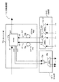
図2は光伝送装置の構成を示す図である。第1の実施の形態の光伝送装置1−1は、光スイッチ部10a、Add部12−1、Drop部13−1から構成される。光スイッチ部10aは、3×3のWSS11aを含む。Add部12−1は、WSS12aおよびスイッチ制御部12bを含む。Drop部13−1は、カプラ13aおよびAWG(Arrayed Waveguide Grating:アレイ導波路型光合分波器)13bを含む(なお、光スイッチ部10a内にも、実際にはWSS11aのスイッチ制御を行うスイッチ制御部が存在するが図示は省略している)。
FIG. 2 is a diagram illustrating a configuration of the optical transmission apparatus. The optical transmission device 1-1 according to the first embodiment includes an
Add部12−1は、異なる波長がn個あり、n個の波長の中で異なるビットレートがk種類あるような挿入光信号(以下、挿入光信号をAdd信号と呼ぶ)のAdd制御を行う場合、n個のn入力ポートおよびk個のk出力ポートを有するn×kのWSSで構成される。 The Add unit 12-1 performs Add control of an inserted optical signal (hereinafter, the inserted optical signal is referred to as an Add signal) having n different wavelengths and k different bit rates among the n wavelengths. Case, it consists of n × k WSS with n n input ports and k k output ports.
ここでは、40Gb/s(以下、40Gと表記)と10Gb/s(以下、10Gと表記)の2種類(k=2)のビットレートが混在しているAdd信号を受信するものとして、Add部12−1は、n×2のWSS12aとしている。
Here, the Add section is assumed to receive an Add signal in which two types (k = 2) of bit rates of 40 Gb / s (hereinafter referred to as 40 G) and 10 Gb / s (hereinafter referred to as 10 G) are mixed. 12-1 is an n × 2
一方、WSS11aの入力ポートin1には、コアネットワークから流れてくる光信号が入力する。入力ポートin2には、WSS11aとAdd部12−1とを接続する方路L1を流れるAdd信号が入力する。入力ポートin3には、WSS11aとAdd部12−1とを接続する方路L2を流れるAdd信号が入力する。
On the other hand, an optical signal flowing from the core network is input to the input port in1 of the WSS 11a. An Add signal that flows through the route L1 that connects the
また、WSS11aでスイッチングされた後の光信号は、出力ポートout1からはコアネットワークへ向かって出力し、出力ポートout2、out3からはDrop部13−1へ向かって出力する。
The optical signal after being switched by the
Drop部13−1は、m入力および1出力のm×1カプラと、m×1カプラから出力された分岐光信号(以下、分岐光信号をDrop信号と呼ぶ)を分波する分波器とから構成される。ここでは、m=2なので、2×1のカプラ13aと、分波器として1入力およびn出力の1×nのAWG13bとで構成されている。
The drop unit 13-1 includes an m × 1 coupler having m inputs and one output, and a demultiplexer that demultiplexes a branched optical signal output from the m × 1 coupler (hereinafter, the branched optical signal is referred to as a Drop signal). Consists of Here, since m = 2, it is composed of a 2 × 1
次にWSS11aの動作について説明する。図3はWSS11aのスイッチング動作を示す図である。コアネットワークを流れてきた光信号をそのままコアネットワークへスルースイッチングする様子を示している。
Next, the operation of the
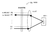
WSS11aは、分光光学系11a−1、レンズ11a−2、ミラー11a−3(ミラー11a−3は、波長毎に存在する)から構成されており、1つの入力ポートから入射された入射光をいずれか1つの出力ポートから出力する。なお、ミラー11a−3は、一般にはMEMS(Micro Electro Mechanical Systems)が使用され、ミラー11a−3の角度を変えることによって、出力ポートの切り替えが行われる。
The
図3の場合、ミラー11a−3の傾きによって、入力ポートin1からの入力信号は、出力ポートout1から出力される。なお、WSSは、その構造上の理由から、隣接ポートに入力された2信号に対する出力先は必ず隣り合うことになるので、2入力信号のうち、一方の出力先を決めると、他方の入力信号の出力先は自動的に決定する。
In the case of FIG. 3, the input signal from the input port in1 is output from the output port out1 due to the inclination of the
例えば、WSS11aの2つの入力ポートin1、in2のうち、外側に位置する入力ポートin1からの入力信号が、出力ポートout1から出力するのであれば、ミラー11a−3の傾きに変化がなければ、内側に位置する入力ポートin2からの入力信号は、出力ポートout1の内側に隣接する出力ポート(この例では該当出力ポートは存在しないが)から出力することになる(出力ポートout2、out3から出力することはない)。
For example, if the input signal from the input port in1 located outside of the two input ports in1 and in2 of the
図4はWSS11aのスイッチング動作を示す図である。コアネットワークを流れてきた光信号をDropし、10GのAdd信号をコアネットワークへ出力する場合のスイッチング状態を示している。
FIG. 4 is a diagram showing a switching operation of the
図4の場合、ミラー11a−3の傾きによって、入力ポートin1からの入力信号は、出力ポートout2から出力される。このとき、入力ポートin1、in2のうち、外側に位置する入力ポートin1からの入力信号が、出力ポートout2から出力するので、ミラー11a−3の傾きに変化がなければ、内側に位置する入力ポートin2からの入力信号(10GのAdd信号)は、出力ポートout2の内側に隣接する出力ポートout1から出力されることになる。
In the case of FIG. 4, the input signal from the input port in1 is output from the output port out2 due to the inclination of the
図5はWSS11aのスイッチング動作を示す図である。コアネットワークを流れてきた光信号をDropし、40GのAdd信号をコアネットワークへ出力する場合のスイッチング状態を示している。
FIG. 5 is a diagram showing the switching operation of the
図5の場合、ミラー11a−3の傾きによって、入力ポートin1からの入力信号は、出力ポートout3から出力される。このとき、2つの入力ポートin1、in3のうち、外側に位置する入力ポートin1からの入力信号が、出力ポートout3から出力するので、ミラー11a−3の傾きに変化がなければ、入力ポートin2を飛ばして内側に位置する入力ポートin3からの入力信号(40GのAdd信号)は、出力ポートout2を飛ばして内側に位置する出力ポートout1から出力されることになる(すなわち、入力ポートへの入射光は、その入力ポートと対照的な位置にある出力ポートから出射される)。
In the case of FIG. 5, the input signal from the input port in1 is output from the output port out3 due to the inclination of the
次にAdd制御について説明する。図2において、Add部12−1内のn×2のWSS12aは、波長λ1〜λnの光信号を受信する(この例では、波長λ1〜λnの各光信号のビットレートは10G、40Gのいずれかである)。そして、スイッチ制御部12bの指示にもとづき、出力ポートP1または出力ポートP2へスイッチングする。
Next, Add control will be described. In FIG. 2, the n × 2
出力ポートP1に接続される光ファイバの方路L1には、10G用の分散補償が施されており、出力ポートP2に接続される光ファイバの方路L2には40G用の分散補償が施されている。具体的には図2の場合、方路L1には、10G用のDCT(Dispersion Compensation Transmitter)14aが設けられ、方路L2には、40G用のDCT14bが設けられている(なお、10Gのビットレートで波長分散の影響が少なく、所望の伝送特性を満たすならば、DCT14aは必ずしも設けなくてもよい)。
The optical fiber route L1 connected to the output port P1 is subjected to 10G dispersion compensation, and the optical fiber route L2 connected to the output port P2 is subjected to 40G dispersion compensation. ing. Specifically, in the case of FIG. 2, a 10G DCT (Dispersion Compensation Transmitter) 14a is provided in the route L1, and a
スイッチ制御部12bは、Addすべき各波長のビットレートをあらかじめ認識しており、そのビットレートに応じて出力ポートP1または出力ポートP2が選択されるように、WSS12aのスイッチ制御を行う。
The
例えば、波長λ1、λ3、λ5、・・・というような、奇数番号の波長のビットレートが10Gであったとすると、スイッチ制御部12bは、波長λ1、λ3、λ5、・・・の波長をAddする際には、これらの波長が出力ポートP1側へスイッチングされるようにWSS12a内のミラーを制御する。
For example, assuming that the bit rate of odd-numbered wavelengths such as wavelengths λ1, λ3, λ5,... Is 10G, the
また、波長λ2、λ4、λ6、・・・というような、偶数番号の波長のビットレートが40Gであった場合には、スイッチ制御部12bは、波長λ2、λ4、λ6、・・・の波長をAddする際には、これらの波長が出力ポートP2側へスイッチングされるようにWSS12a内のミラーを制御する。
Further, when the bit rate of the even-numbered wavelengths such as the wavelengths λ2, λ4, λ6,... Is 40G, the
WSS12aは、スイッチ制御部12bの指示にもとづき、スイッチングを行う。そして、WSS12aより出力された10Gおよび40GのWDMの光信号は、分散補償値が最適値に設定されたDCT14a、14bのそれぞれを通過することで、一括した前置分散補償が行われることになる。
The
図6、図7はWSS12aのスイッチング動作例を示す図である。図6では、波長λ1が10Gのビットレートの場合であり、出力ポートP1から波長λ1が出力される様子が示されている。なお、例えば、波長λ2も10Gならば、ミラーの傾きを変化させて、出力ポートP1から波長λ2を出力させることになる。
6 and 7 are diagrams showing an example of the switching operation of the
図7では、波長λ1が40Gのビットレートの場合、出力ポートP2から波長λ1が出力される様子が示されている。なお、例えば、波長λ2も40Gならば、ミラーの傾きを変化させて、出力ポートP2から波長λ2を出力させることになる。 FIG. 7 shows a state where the wavelength λ1 is output from the output port P2 when the wavelength λ1 is a 40 G bit rate. For example, if the wavelength λ2 is also 40 G, the wavelength λ2 is output from the output port P2 by changing the tilt of the mirror.
このように、10G、40Gのビットレートに対応して分散補償を行うDCT14a、14bを、各ビットレートの波長が通過する方路L1、L2に設置し、Add部12−1において、Add信号のビットレートと同じビットレートの分散補償を行う方路L1、L2が選択されるようにスイッチングを行って、選択した方路を介して、Add信号をWSS11aへ送信する構成とした。
In this way,
従来のOADMシステムでは、各ビットレートに対応したDCTを、光ファイバ方路それぞれに配置して分散補償を行っていたが、上記のような構成にすることにより、一括して効率よく分散補償を行うことができるので、装置規模およびコストの削減を行うことが可能になる。 In a conventional OADM system, DCT corresponding to each bit rate is arranged in each optical fiber route to perform dispersion compensation. By adopting the configuration as described above, dispersion compensation can be efficiently performed collectively. Therefore, it is possible to reduce the scale and cost of the apparatus.
次にDrop制御について説明する。図2において、カプラ13aの2入力部分は、WSS11aの出力ポートout2、out3と接続して、出力ポートout2、out3から送信された光信号を合波して、AWG13bへ送信する。AWG13bは、カプラ13aからの出力信号を複数に分波して出力(Drop)する。
Next, Drop control will be described. In FIG. 2, the two input portions of the
ここで、図4で上述したWSS11aの動作では、入力ポートin1から入力した光信号は、出力ポートout2から出力し、図5で上述したWSS11aの動作では、入力ポートin1から入力した光信号は、出力ポートout3から出力する。
Here, in the operation of the
このように、入力ポートin1から入力した光信号の出力ポートは、それぞれWSS11aのミラーの傾き状態(スイッチング状態)によって異なることになるが、カプラ13aを用いて、出力ポートout2、out3からの出力信号を結合しているので、どちらの出力ポートout2、out3から出力された光信号でもDropすることが可能である。
As described above, the output port of the optical signal input from the input port in1 differs depending on the mirror tilt state (switching state) of the
次に第2の実施の形態について説明する。なお、以降の説明では、すでに上述した構成要素には同じ符号を付けて重複する構成要素の説明は省略する。図8は光伝送装置の構成を示す図である。第2の実施の形態の光伝送装置1−2は、光スイッチ部10a、Add部12−2、Drop部13−1から構成される。
Next, a second embodiment will be described. In the following description, the same reference numerals are given to the components already described above, and description of the overlapping components will be omitted. FIG. 8 is a diagram illustrating a configuration of the optical transmission apparatus. The optical transmission device 1-2 according to the second embodiment includes an
Add部12−2は、異なるビットレートがk種類あり、k種類のビットレート毎に異なる波長がn個あるような光信号をAdd制御する場合、n個のn入力ポートおよび1個の1出力ポートを有するn×1のAWGをk台用いて構成される。 When the Add unit 12-2 performs Add control of an optical signal having k types of different bit rates and having n different wavelengths for each of the k types of bit rates, the n unit has n input ports and one output. It is configured using k n × 1 AWGs having ports.
ここの例では、10G、40Gのビットレートによってk=2なので、n×1のAWG12c−1、12c−2の2台としている。AWG12c−1は、方路L1と接続し、AWG12c−2は、方路L2と接続する。
In this example, since k = 2 depending on the bit rates of 10G and 40G, there are two
AWG12c−1は、10Gの波長λ1〜λnを合波して合波信号を生成し、10Gの分散補償を行うDCT14aが設置された方路L1を介して、WSS11aへ向けて合波信号を送信してAddする。また、AWG12c−2は、40Gの波長λ1〜λnを合波して合波信号を生成し、40Gの分散補償を行うDCT14bが設置された方路L2を介して、WSS11aへ向けて合波信号を送信してAddする。
The
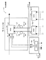
次に第3の実施の形態について説明する。図9は光伝送装置の構成を示す図である。第3の実施の形態の光伝送装置1−3は、光スイッチ部10a、Add部12−3、Drop部13−3から構成される。
Next, a third embodiment will be described. FIG. 9 is a diagram illustrating a configuration of the optical transmission apparatus. The optical transmission device 1-3 according to the third embodiment includes an
Add部12−3は、n個の異なる波長からなる波長グループがA個あり、波長グループ毎に異なるビットレートがk種類あるような光信号のAdd制御を行う場合、n個のn入力ポートおよび1個の1出力ポートを有するn×1のWSSをA台と、A個のA入力ポートおよびk個のk出力ポートを有するA×kのWSSの1台と、から構成される。 When the Add unit 12-3 performs Add control of an optical signal in which there are A wavelength groups composed of n different wavelengths and there are k kinds of different bit rates for each wavelength group, the n input ports and It is composed of an n × 1 WSS having one 1 output port and one A × k WSS having A A input ports and k k output ports.
したがって、Add部12−3は、10G、40Gのビットレートでk=2なので、n×1のWSS12d−1〜12d−AのA台と、A×2のWSS12eの1台とを含み、さらにWSS12eおよびWSS12d−1〜12d−Aのスイッチ制御を行うスイッチ制御部12fを備えている(なお、WSSのスイッチ制御を行うスイッチ制御部は、実際には光スイッチ部10aおよびDrop部13−3にも存在するが図示では省略している)。
Therefore, the add unit 12-3 includes 10 units of n × 1
WSS12d−1〜12d−Aのそれぞれは、波長λ1〜λnからなる波長グループの光信号をスイッチングして、1つの出力ポートからWDM信号をWSS12eへ出力する。
Each of the
スイッチ制御部12fは、Addすべき波長グループのビットレートをあらかじめ認識しており、そのビットレートに応じて出力ポートP1または出力ポートP2が選択されるように、WSS12eのスイッチ制御を行う。
The
例えば、WSS12d−1がスイッチング対象とする波長グループ(波長グループg1とする)が10Gのビットレートであれば、スイッチ制御部12fは、波長グループg1をAddする際には、出力ポートP1側へスイッチングさせるようにWSS12e内のミラーを制御する。
For example, if the wavelength group to be switched by WSS12d-1 (referred to as wavelength group g1) is a 10G bit rate, the
また、WSS12d−2がスイッチング対象とする波長グループ(波長グループループg2とする)が40Gのビットレートであれば、スイッチ制御部12fは、波長グループg2をAddする際には、出力ポートP2側へスイッチングさせるようにWSS12e内のミラーを制御する。
If the wavelength group to be switched by
WSS12eは、スイッチ制御部12fの指示にもとづき、スイッチングを行う。そして、WSS12eより出力された10Gおよび40GのWDMの光信号は、分散補償値が最適値に設定されたDCT14a、14bのそれぞれを通過することで、一括した前置分散補償が行われることになる。
The
一方、Drop部13−3は、カプラ13aと、1×AのWSS13cと、1×nのWSS13d−1〜13d−Aとから構成される。カプラ13aの2入力部分は、WSS11aの出力ポートout2、out3と接続して、出力ポートout2、out3から送信された光信号を合波して、WSS13cへ送信する。WSS13cは、カプラ13aからの出力信号を受信しスイッチングして出力し、WSS13d−1〜13d−Aは、WSS13cからの出力信号を受信し、波長グループ毎にスイッチングして出力(Drop)する。
On the other hand, the drop unit 13-3 includes a
次に第4の実施の形態について説明する。図10は光伝送装置の構成を示す図である。第4の実施の形態の光伝送装置1−4は、光スイッチ部10a、Add部12−4、Drop部13−4から構成される(光スイッチ部10a、Add部12−4、Drop部13−4内に存在するスイッチ制御部の図示は省略している)。
Next, a fourth embodiment will be described. FIG. 10 is a diagram illustrating a configuration of the optical transmission apparatus. The optical transmission device 1-4 according to the fourth embodiment includes an
Add部12−4は、異なる波長がa個で低ビットレートのAdd光信号である低ビットレートAdd信号と、異なる波長がb個で高ビットレートのAdd信号である高ビットレートAdd信号とのAdd制御を行う場合、a個のa入力ポートおよび1個の1出力ポートを有する透過帯域幅の狭い低ビットレート用WSSと、b個のb入力ポートおよび1個の1出力ポートを有する透過帯域幅の広い高ビットレート用WSSとから構成される。 The Add unit 12-4 includes a low bit rate Add signal that is an Add optical signal with a low wavelength and a low bit rate, and a high bit rate Add signal that is an Add signal with a high number of different wavelengths and b. When performing Add control, WSS for low bit rate with a narrow transmission bandwidth having a number of a input ports and one output port, and a transmission band having b number of b input ports and one output port. It is composed of a wide WSS for high bit rate.
ここの例では、a=b=nとし、10GビットレートのAddを行うWSS12g−1が透過帯域幅の狭い低ビットレート用のWSSに該当し、40GビットレートのAddを行うWSS12g−2が透過帯域幅の広い高ビットレート用のWSSに該当する。 In this example, a = b = n, WSS12g-1 performing Add of 10G bit rate corresponds to WSS for low bit rate having a narrow transmission bandwidth, and WSS12g-2 performing Add of 40G bit rate is transmitted. This corresponds to a WSS for a wide bit rate and a high bit rate.
このように、低ビットレートのAdd信号に対しては、コストが安い透過帯域幅の狭いWSSを使用し、高ビットレートのAdd信号に対しては、コストが高い透過帯域幅の広いWSSを使用するというように、透過帯域幅の違うWSSを使い分けて構成することにより、コストの削減を図ることが可能になる。 In this way, a low-cost low-transmission bandwidth WSS is used for low bit-rate Add signals, and a high-cost wide-transmission bandwidth WSS is used for high-bit-rate Add signals. As described above, the cost can be reduced by using different WSSs having different transmission bandwidths.
なお、Add動作としては、WSS12g−1でスイッチング出力された10GのWDM信号は、10Gの分散補償値が最適値に設定されたDCT14aを通過することで、一括した前置分散補償が行われ、WSS12g−2でスイッチング出力された40GのWDM信号は、40Gの分散補償値が最適値に設定されたDCT14bを通過することで、一括した前置分散補償が行われる。
As an Add operation, the 10G WDM signal that is switched and output by the
また、Drop動作としては、カプラ13aの2入力部分は、WSS11aの出力ポートout2、out3と接続して、出力ポートout2、out3から送信された光信号を合波して、WSS13eへ送信する。WSS13eは、カプラ13aからの出力信号を受信しスイッチングして出力(Drop)する。
As a drop operation, the two input portions of the
次に光伝送装置1の変形例について説明する。図1の光伝送装置1では、ビットレート毎に分散補償を設定したが、変形例の場合は、Add信号がAdd部に到達するまでの伝送距離毎(各伝送距離で生じる波長分散毎)に分散補償を設定するものである。なお、伝送距離は伝送スパン数としてもよい。
Next, a modification of the
図11は光伝送装置の変形例を示す図である。光伝送装置2は、光スイッチ部20、Add部22、Drop部23から構成され、光信号の分岐(Drop)、挿入(Add)によるOADMを行って光伝送を行う装置である。なお、光伝送装置1が伝送制御する光信号はWDM信号である。
FIG. 11 is a diagram illustrating a modification of the optical transmission apparatus. The
光スイッチ部20は、N×MのWSS21を含む。Add部22は、Add信号の伝送距離に応じて発生する波長分散がk種類ある場合に、N入力ポートの内、k(<N)個のk入力ポートと接続して、n入力ポートへAdd信号を送信してAdd制御を行う。Drop部23は、M出力ポートの内、m(<M)個のm出力ポートと接続して、m出力ポートから送信された光信号のDrop制御を行う。
The
ここで、WSS21のk入力ポートと、Add部22と、を接続するk個の方路それぞれには、伝送距離に応じて発生する波長分散毎に対応した分散補償を設定し、Add部22は、Add信号の分散補償を行う方路を選択して、選択した方路を介して、Add信号をWSS21へ送信する。
Here, in each of k routes connecting the k input port of the
例えば、処理対象のAdd信号λ1が、伝送距離D1[km]の光ファイバ上を流れてきてAdd部22に到達するのであれば、伝送距離D1[km]で生じる波長分散を分散補償するための分散補償を、方路L1に設定しておき、Add部22は、Add信号λ1のAdd時には、方路L1を選択する。これによって、Add信号λ1は、方路L1を介して、WSS21へ送信される途中で分散補償されることになる。
For example, if the Add signal λ1 to be processed flows on the optical fiber having the transmission distance D1 [km] and reaches the
また、処理対象のAdd信号λ2が、伝送距離D2[km]の光ファイバ上を流れてきてAdd部22に到達するのであれば、伝送距離D2[km]で生じる波長分散を分散補償するための分散補償を、方路L2に設定しておき、Add部22は、Add信号λ2のAdd時には、方路L2を選択する。これによって、Add信号λ2は、方路L2を介して、WSS21へ送信される途中で分散補償されることになる。
Further, if the Add signal λ2 to be processed flows on the optical fiber having the transmission distance D2 [km] and reaches the
このように、ビットレート毎に分散補償を設定する代わりに、Add部に到達するまでの各伝送距離で生じる波長分散毎に、WSS21のk入力ポートと、Add部22と、を接続するk個の方路それぞれに、分散補償を設定する構成としてもよい。なお、変形例における、光スイッチ部20、Add部22、Drop23の構成は、上述した第1の実施の形態〜第4の実施の形態で示した、光スイッチ部、Add部およびDrop部の構成と同じ構成を適用でき、変形例の光伝送装置2は、方路L1〜Lkに設定する分散補償の設定思想のみが光伝送装置1と異なるものである。
In this way, instead of setting dispersion compensation for each bit rate, k units connecting the k input port of the
上記については単に本発明の原理を示すものである。さらに、多数の変形、変更が当業者にとって可能であり、本発明は上記に示し、説明した正確な構成および応用例に限定されるものではなく、対応するすべての変形例および均等物は、添付の請求項およびその均等物による本発明の範囲とみなされる。 The above merely illustrates the principle of the present invention. In addition, many modifications and changes can be made by those skilled in the art, and the present invention is not limited to the precise configuration and application shown and described above, and all corresponding modifications and equivalents may be And the equivalents thereof are considered to be within the scope of the invention.
1 光伝送装置
10 光スイッチ部
11 N×M波長選択スイッチ
12 挿入制御部
13 分岐制御部
L1〜Lk 方路DESCRIPTION OF
Claims (15)
N個のN入力ポートおよびM個のM出力ポートを有するN×M波長選択スイッチを含む光スイッチ部と、
挿入すべき光信号である挿入光信号のビットレートがk(≧2)種類あり、前記N入力ポートの内、k(<N)個のk入力ポートと接続して、前記k入力ポートへ前記挿入光信号を送信して挿入制御を行う挿入制御部と、
前記M出力ポートの内、m(<M)個のm出力ポートと接続して、前記m出力ポートから送信された光信号の分岐制御を行う分岐制御部と、
を有し、
前記N×M波長選択スイッチの前記k入力ポートと、前記挿入制御部と、を接続するk個の方路それぞれには、ビットレート毎に対応した波長分散を低減するための分散低減を設定し、
前記挿入制御部は、前記挿入光信号の分散低減を行う前記方路を介して、前記挿入光信号を前記N×M波長選択スイッチへ送信する、
ことを特徴とする光伝送装置。In an optical transmission device that performs optical transmission by branching and inserting optical signals,
An optical switch unit including an N × M wavelength selective switch having N N input ports and M M output ports;
The bit rate of an optical signal to be inserted insertion optical signal is k (≧ 2) kinds Ah is, among the N input ports, k connected to the (<N) number of k input ports, to said k input ports An insertion control unit for performing insertion control by transmitting the insertion optical signal;
A branch controller connected to m (<M) m output ports of the M output ports and performing branch control of an optical signal transmitted from the m output ports;
Have
It said k input ports of the N × M wavelength selective switch, the insertion control unit, into k routes each connecting a, set the variance reduction for reducing the chromatic dispersion corresponding to each bit rate ,
The insertion control unit, the variance reduction of the insertion optical signal via the line cormorants before Symbol route, transmits the insertion optical signal into the N × M wavelength selective switch,
An optical transmission device characterized by that.
A台の前記n×1波長選択スイッチの各出力ポートは、前記A×k波長選択スイッチの前記A入力ポートにそれぞれ接続し、 Each output port of the A × n wavelength selective switch is connected to the A input port of the A × k wavelength selective switch,
n個の異なる波長からなる波長グループがA個で、前記波長グループ毎に異なるビットレートがk種類ある前記挿入光信号の挿入制御を行うことを特徴とする請求項1記載の光伝送装置。 2. The optical transmission device according to claim 1, wherein insertion control of the inserted optical signal having A wavelength groups consisting of n different wavelengths and k kinds of different bit rates for each wavelength group is performed.
N個のN入力ポートおよびM個のM出力ポートを有するN×M波長選択スイッチを含む光スイッチ部と、
挿入すべき光信号である挿入光信号の伝送距離に応じて発生する波長分散がk(≧2)種類あり、前記N入力ポートの内、k(<N)個のk入力ポートと接続して、前記k入力ポートへ前記挿入光信号を送信して挿入制御を行う挿入制御部と、
前記M出力ポートの内、m(<M)個のm出力ポートと接続して、前記m出力ポートから送信された光信号の分岐制御を行う分岐制御部と、
を有し、
前記N×M波長選択スイッチの前記k入力ポートと、前記挿入制御部と、を接続するk個の方路それぞれには、前記挿入光信号が前記挿入制御部に到達するまでに流れてきた光ファイバ上の伝送距離に応じて発生する前記波長分散毎に対応した分散低減を設定し、
前記挿入制御部は、前記挿入光信号の分散低減を行う前記方路を介して、前記挿入光信号を前記N×M波長選択スイッチへ送信する、
ことを特徴とする光伝送装置。In an optical transmission device that performs optical transmission by branching and inserting optical signals,
An optical switch unit including an N × M wavelength selective switch having N N input ports and M M output ports;
Wavelength dispersion that occurs in response to the transmission distance of an optical signal to be inserted insertion optical signal is k (≧ 2) kinds Ah is, among the N input ports, k is connected to the (<N) number of k input ports An insertion control unit for performing insertion control by transmitting the insertion optical signal to the k input port;
A branch controller connected to m (<M) m output ports of the M output ports and performing branch control of an optical signal transmitted from the m output ports;
Have
Light that has flowed until the insertion optical signal reaches the insertion control unit in each of k paths connecting the k input port of the N × M wavelength selective switch and the insertion control unit. Set the dispersion reduction corresponding to each chromatic dispersion generated according to the transmission distance on the fiber,
The insertion control unit, then through the route to perform the variance reduction of the insertion optical signal, and transmits the insertion optical signal into the N × M wavelength selective switch,
An optical transmission device characterized by that.
A台の前記n×1波長選択スイッチの各出力ポートは、前記A×k波長選択スイッチの前記A入力ポートにそれぞれ接続し、 Each output port of the A × n wavelength selective switch is connected to the A input port of the A × k wavelength selective switch,
n個の異なる波長からなる波長グループがA個で、前記波長グループ毎に異なる波長分散がk種類ある前記挿入光信号の挿入制御を行うことを特徴とする請求項9記載の光伝送装置。 10. The optical transmission apparatus according to claim 9, wherein insertion control of the inserted optical signal having A wavelength groups consisting of n different wavelengths and k types of chromatic dispersions different for each wavelength group is performed.
Applications Claiming Priority (1)
| Application Number | Priority Date | Filing Date | Title |
|---|---|---|---|
| PCT/JP2007/055403 WO2008114352A1 (en) | 2007-03-16 | 2007-03-16 | Optical transmission device |
Publications (2)
| Publication Number | Publication Date |
|---|---|
| JPWO2008114352A1 JPWO2008114352A1 (en) | 2010-06-24 |
| JP4796183B2 true JP4796183B2 (en) | 2011-10-19 |
Family
ID=39765474
Family Applications (1)
| Application Number | Title | Priority Date | Filing Date |
|---|---|---|---|
| JP2009504952A Expired - Fee Related JP4796183B2 (en) | 2007-03-16 | 2007-03-16 | Optical transmission equipment |
Country Status (4)
| Country | Link |
|---|---|
| US (1) | US8295703B2 (en) |
| EP (1) | EP2124355B1 (en) |
| JP (1) | JP4796183B2 (en) |
| WO (1) | WO2008114352A1 (en) |
Families Citing this family (9)
| Publication number | Priority date | Publication date | Assignee | Title |
|---|---|---|---|---|
| US8131151B2 (en) * | 2009-10-09 | 2012-03-06 | Fujitsu Limited | Testing and measurement in optical networks |
| JP5636712B2 (en) * | 2010-03-23 | 2014-12-10 | 富士通株式会社 | Signal light processing apparatus, optical transmission apparatus, and signal light processing method |
| US20120087658A1 (en) * | 2010-10-12 | 2012-04-12 | Tyco Electronics Subsea Communications Llc | Wavelength Selective Switch Band Aggregator and Band Deaggregator and Systems and Methods Using Same |
| US8731402B2 (en) * | 2010-10-12 | 2014-05-20 | Tyco Electronics Subsea Communications Llc | Orthogonally-combining wavelength selective switch multiplexer and systems and methods using same |
| JP5650806B2 (en) * | 2012-06-06 | 2015-01-07 | ゼットティーイー(ユーエスエー)インコーポレーテッド | Method and apparatus for pre-equalization and post-equalization in an optical communication system |
| JPWO2013186842A1 (en) * | 2012-06-11 | 2016-02-01 | 富士通株式会社 | Optical transmission equipment |
| JP2014022865A (en) * | 2012-07-17 | 2014-02-03 | Nec Corp | Optical signal branching device and optical signal insertion device |
| US9525490B2 (en) * | 2012-07-26 | 2016-12-20 | Aurrion, Inc. | Reconfigurable optical transmitter |
| US10237633B2 (en) * | 2017-02-16 | 2019-03-19 | Ciena Corporation | Systems and methods for modular deployment and upgrade of multiple optical spectrum bands in optical transmission systems |
Citations (4)
| Publication number | Priority date | Publication date | Assignee | Title |
|---|---|---|---|---|
| JPH09261173A (en) * | 1996-03-27 | 1997-10-03 | Nec Corp | Optical transmitting device |
| JP2005295126A (en) * | 2004-03-31 | 2005-10-20 | Fujitsu Ltd | Dispersion compensation method and compensation node apparatus |
| JP2006042012A (en) * | 2004-07-28 | 2006-02-09 | Nec Corp | Optical communication device, optical transmission system, and optical transmission method |
| JP2006086920A (en) * | 2004-09-17 | 2006-03-30 | Fujitsu Ltd | Optical demultiplexing method, optical multiplexing method and optical transmission device |
Family Cites Families (7)
| Publication number | Priority date | Publication date | Assignee | Title |
|---|---|---|---|---|
| JP2002208895A (en) * | 2001-01-10 | 2002-07-26 | Fujitsu Ltd | Optical add/drop device |
| JP4676657B2 (en) * | 2001-08-30 | 2011-04-27 | 富士通株式会社 | Optical add / drop multiplexer |
| US6999681B2 (en) * | 2002-01-23 | 2006-02-14 | Pts Corporation | Method of seamless migration from static to agile optical networking |
| JP4259186B2 (en) * | 2002-08-29 | 2009-04-30 | 住友電気工業株式会社 | Optical transmission system |
| US7308197B1 (en) * | 2003-01-31 | 2007-12-11 | Ciena Corporation | Modular add/drop multiplexer including a wavelength selective switch |
| JP2004254018A (en) * | 2003-02-19 | 2004-09-09 | Fujitsu Ltd | Dispersion compensating device and wavelength division multiplex communication system using the same |
| JP4750613B2 (en) * | 2006-04-21 | 2011-08-17 | 富士通株式会社 | Polarization scrambler, optical add / drop device, optical path switching device, and wavelength division multiplexing optical transmission system |
-
2007
- 2007-03-16 JP JP2009504952A patent/JP4796183B2/en not_active Expired - Fee Related
- 2007-03-16 WO PCT/JP2007/055403 patent/WO2008114352A1/en active Application Filing
- 2007-03-16 EP EP07738848.6A patent/EP2124355B1/en not_active Not-in-force
-
2009
- 2009-09-02 US US12/585,084 patent/US8295703B2/en not_active Expired - Fee Related
Patent Citations (4)
| Publication number | Priority date | Publication date | Assignee | Title |
|---|---|---|---|---|
| JPH09261173A (en) * | 1996-03-27 | 1997-10-03 | Nec Corp | Optical transmitting device |
| JP2005295126A (en) * | 2004-03-31 | 2005-10-20 | Fujitsu Ltd | Dispersion compensation method and compensation node apparatus |
| JP2006042012A (en) * | 2004-07-28 | 2006-02-09 | Nec Corp | Optical communication device, optical transmission system, and optical transmission method |
| JP2006086920A (en) * | 2004-09-17 | 2006-03-30 | Fujitsu Ltd | Optical demultiplexing method, optical multiplexing method and optical transmission device |
Also Published As
| Publication number | Publication date |
|---|---|
| EP2124355B1 (en) | 2016-12-14 |
| WO2008114352A1 (en) | 2008-09-25 |
| US20100028007A1 (en) | 2010-02-04 |
| JPWO2008114352A1 (en) | 2010-06-24 |
| EP2124355A4 (en) | 2012-07-04 |
| EP2124355A1 (en) | 2009-11-25 |
| US8295703B2 (en) | 2012-10-23 |
Similar Documents
| Publication | Publication Date | Title |
|---|---|---|
| JP4796183B2 (en) | Optical transmission equipment | |
| JP6060648B2 (en) | Optical drop device, optical add device and optical add / drop device | |
| JP5682256B2 (en) | Optical insertion device and optical branching device | |
| US9252910B2 (en) | Expandable multicast optical switch | |
| JP5287993B2 (en) | Optical signal transmitter, optical signal receiver, wavelength division multiplexing optical communication device, and wavelength path system | |
| JP2007148042A (en) | Wavelength selective optical switch, optical multiplexer, optical demultiplexer, and wavelength selective optical switch module | |
| JP5002431B2 (en) | Optical transmission system | |
| JP4152932B2 (en) | Optical demultiplexing method, optical multiplexing method, and optical transmission device using the same | |
| JP4730145B2 (en) | Optical signal switching device and optical signal switching method | |
| WO2014141281A1 (en) | Routing in an sdm optical communication network | |
| JP5273679B2 (en) | Routing method for node device for optical communication network and node device for optical communication network | |
| JP2010103640A (en) | Optical repeater | |
| US9025915B2 (en) | Method and module for switching optical signals having different modes of propagation | |
| JP4852260B2 (en) | Single-core bidirectional wavelength division multiplexing transmission system | |
| JP4852491B2 (en) | Optical cross-connect switch functional unit and optical cross-connect device | |
| CN110024312B (en) | Optical transmission apparatus and optical transmission method | |
| JP2004135331A (en) | Optical cross-connect system | |
| JP5023021B2 (en) | Optical add / drop multiplexer and optical level adjustment method | |
| JP5622197B2 (en) | Hierarchical optical path cross-connect equipment for optical path networks | |
| JP5340369B2 (en) | Optical repeater | |
| JP2010130575A (en) | Transparent optical network, node device, and method for monitoring fault of transparent optical network | |
| JP6464594B2 (en) | Node optical switch device and optical switch method | |
| JP4447021B2 (en) | Optical wavelength multiplexer / demultiplexer | |
| JPH1132354A (en) | Optical cross connector | |
| JP2010011486A (en) | Optical communications network |
Legal Events
| Date | Code | Title | Description |
|---|---|---|---|
| A131 | Notification of reasons for refusal |
Free format text: JAPANESE INTERMEDIATE CODE: A131 Effective date: 20110308 |
|
| A521 | Written amendment |
Free format text: JAPANESE INTERMEDIATE CODE: A523 Effective date: 20110509 |
|
| TRDD | Decision of grant or rejection written | ||
| A01 | Written decision to grant a patent or to grant a registration (utility model) |
Free format text: JAPANESE INTERMEDIATE CODE: A01 Effective date: 20110726 |
|
| A01 | Written decision to grant a patent or to grant a registration (utility model) |
Free format text: JAPANESE INTERMEDIATE CODE: A01 |
|
| A61 | First payment of annual fees (during grant procedure) |
Free format text: JAPANESE INTERMEDIATE CODE: A61 Effective date: 20110728 |
|
| R150 | Certificate of patent or registration of utility model |
Free format text: JAPANESE INTERMEDIATE CODE: R150 |
|
| FPAY | Renewal fee payment (event date is renewal date of database) |
Free format text: PAYMENT UNTIL: 20140805 Year of fee payment: 3 |
|
| LAPS | Cancellation because of no payment of annual fees |