JP4780098B2 - Microcomputer - Google Patents
Microcomputer Download PDFInfo
- Publication number
- JP4780098B2 JP4780098B2 JP2007322364A JP2007322364A JP4780098B2 JP 4780098 B2 JP4780098 B2 JP 4780098B2 JP 2007322364 A JP2007322364 A JP 2007322364A JP 2007322364 A JP2007322364 A JP 2007322364A JP 4780098 B2 JP4780098 B2 JP 4780098B2
- Authority
- JP
- Japan
- Prior art keywords
- cpu
- data
- circuit
- oscillation
- signal
- Prior art date
- Legal status (The legal status is an assumption and is not a legal conclusion. Google has not performed a legal analysis and makes no representation as to the accuracy of the status listed.)
- Expired - Fee Related
Links
Images

Classifications
-
- Y—GENERAL TAGGING OF NEW TECHNOLOGICAL DEVELOPMENTS; GENERAL TAGGING OF CROSS-SECTIONAL TECHNOLOGIES SPANNING OVER SEVERAL SECTIONS OF THE IPC; TECHNICAL SUBJECTS COVERED BY FORMER USPC CROSS-REFERENCE ART COLLECTIONS [XRACs] AND DIGESTS
- Y02—TECHNOLOGIES OR APPLICATIONS FOR MITIGATION OR ADAPTATION AGAINST CLIMATE CHANGE
- Y02D—CLIMATE CHANGE MITIGATION TECHNOLOGIES IN INFORMATION AND COMMUNICATION TECHNOLOGIES [ICT], I.E. INFORMATION AND COMMUNICATION TECHNOLOGIES AIMING AT THE REDUCTION OF THEIR OWN ENERGY USE
- Y02D10/00—Energy efficient computing, e.g. low power processors, power management or thermal management
Landscapes
- Power Sources (AREA)
- Microcomputers (AREA)
Description
本発明は、内部状態を保持したまま動作を一時的に停止する低消費電力モードの設定が可能に構成されるCPUを備えてなるマイクロコンピュータに関する。 The present invention relates to a microcomputer including a CPU configured to be able to set a low power consumption mode in which an operation is temporarily stopped while maintaining an internal state.
マイクロコンピュータにおいては、CPUが処理を行なう必要がない状態となった場合に、その内部状態を保持しつつクロック信号の発振動作を停止させることで電力消費を低減する低消費電力モードに移行することが可能に構成されているものがある(例えば、特許文献1)。
また、マイクロコンピュータは、外部信号出力端子のレベルを変化させることで、その端子に接続されている外部デバイスの制御を行う。この場合、端子の出力レベルと、その端子をアクティブにする期間とはプログラムによって設定される。
In a microcomputer, when the CPU does not need to perform processing, the microcomputer shifts to a low power consumption mode that reduces power consumption by stopping the oscillation operation of the clock signal while maintaining the internal state. Is configured to be possible (for example, Patent Document 1).
Further, the microcomputer controls the external device connected to the terminal by changing the level of the external signal output terminal. In this case, the output level of the terminal and the period during which the terminal is active are set by the program.
特にバッテリを動作用電源として構成されるマイクロコンピュータでは、CPUが処理を行なう必要がない状態となった場合に、その内部状態を保持しつつクロック信号の発振動作を停止させることで電力消費を低減する低消費電力モードに移行することが可能に構成されているものがある。その場合、マイコンの内部処理や外部デバイスの制御などについては、例えば図37に示すように、低消費電力モードと通常モードとを交互に移行することで、定期的に実行されるようにスケジューリングすることが可能である。
或いは、マイコンの外部で発生する何らかのイベントに応じて不定期に処理を行なう必要がある場合は、そのイベントを低消費電力モードの解除要因とすることで、イベントの発生に応じて通常モードに移行させ、処理を実行させることも可能である。
Alternatively, if it is necessary to perform processing irregularly in response to some event that occurs outside the microcomputer, the event can be used as a factor to cancel the low power consumption mode, so that the normal mode can be entered when the event occurs. It is also possible to execute processing.
しかしながら、特許文献1のような従来のマイクロコンピュータでは、低消費電力モードに移行している期間において外来ノイズが印加されると、外部出力端子の出力レベルが変化してしまうおそれがあった。例えば、マイコンがモータを駆動する制御するように構成されていると、低消費電力モードに移行する場合はモータの回転を停止させるように外部出力端子のレベルを制御する。その状態で、外来ノイズの影響で外部出力端子の出力レベルが変化すると、モータが回転してしまうことになる。
However, in the conventional microcomputer as disclosed in
また、例えば、通常モードにおいてプログラムが実行されている場合は、そのプログラムにおいて外部出力端子のレベルを設定し(例えば、H)、出力期間の間はそのレベルを保持し、出力期間が終了すると前記レベルを元に戻すように設定する(例えば、L)。そして、上記出力期間を把握するために、プログラムはCPUの動作クロック(マシンクロック)などに基づいて動作するタイマを使用する。
また、プログラムは、上記出力期間中においては、他の処理も並行して実行することが可能であるが、そのように並行して実行可能な処理が常に存在するとは限らない。その場合は、結果として、単に端子の出力レベルを保持するためだけにCPUが起動していることになる。そして、その期間中は動作クロックが発振し続けるため、消費電流が増大するという問題があった。
For example, when the program is executed in the normal mode, the level of the external output terminal is set in the program (for example, H), the level is held during the output period, and when the output period ends, the level is Set the level back (for example, L). And in order to grasp | ascertain the said output period, a program uses the timer which operate | moves based on the operation clock (machine clock) etc. of CPU.
Further, the program can execute other processes in parallel during the output period, but such a process that can be executed in parallel does not always exist. In that case, as a result, the CPU is activated only to hold the output level of the terminal. In addition, since the operation clock continues to oscillate during the period, there is a problem that current consumption increases.
本発明は上記事情に鑑みてなされたものであり、その目的は、低消費電力モードの設定が可能に構成される場合に、外来ノイズの影響を極力低減することができるマイクロコンピュータ、また、低消費電力モードに移行している状態においても、外部出力端子のレベル設定を行うことが可能なマイクロコンピュータを提供することにある。 The present invention has been made in view of the above circumstances, and an object of the present invention is to provide a microcomputer capable of reducing the influence of external noise as much as possible when the low power consumption mode is set. An object of the present invention is to provide a microcomputer capable of setting the level of an external output terminal even in a state of shifting to a power consumption mode.
請求項1記載のマイクロコンピュータによれば、信号レベル変化手段は、CPUが低消費電力モードに設定されている期間内に、外部信号出力端子のレベルを変化させる。従って、CPUは、外部信号出力端子のレベルを変化させるためだけに通常の動作モードを継続する必要がないので、消費電力を低減することができる。 According to the microcomputer of the first aspect , the signal level changing means changes the level of the external signal output terminal within a period in which the CPU is set in the low power consumption mode. Therefore, since the CPU does not need to continue the normal operation mode only for changing the level of the external signal output terminal, the power consumption can be reduced.
請求項1記載のマイクロコンピュータによれば、信号レベル変化手段は、レベル変化用タイマのカウント値とレベル変化タイミングが設定されているレジスタの値とを比較回路が比較し、両者が一致することでトリガ信号が出力されると外部信号出力端子のレベルを変化させる。従って、レジスタに設定されるタイミングで、出力端子のレベルを変化させることができる。 According to the microcomputer of the first aspect , the signal level changing means compares the count value of the level change timer with the value of the register in which the level change timing is set, and the two match each other. When the trigger signal is output, the level of the external signal output terminal is changed. Therefore, the level of the output terminal can be changed at the timing set in the register.
請求項2記載のマイクロコンピュータによれば、レジスタは、CPUによって任意のデータ値が設定可能に構成されるので、ユーザプログラムによってレベル変化タイミングを任意に設定することができる。 According to the microcomputer of the second aspect , since the register is configured such that an arbitrary data value can be set by the CPU, the level change timing can be arbitrarily set by the user program.
請求項3記載のマイクロコンピュータによれば、外部信号出力端子のレベルは、低消費電力モードが解除されるとCPUによってリセットすることが可能に構成されるので、CPUが必要な処理を行った時点で出力端子のレベルを直ちにリセットすることができる。 According to the microcomputer of the third aspect, the level of the external signal output terminal can be reset by the CPU when the low power consumption mode is canceled, so that the time point when the CPU performs necessary processing. The output terminal level can be reset immediately.
請求項4記載のマイクロコンピュータによれば、割り込み発生手段は、信号レベル変化手段が外部信号出力端子のレベルを変化させた後、解除要因の発生によって低消費電力モードが解除されると、解除タイマによって低消費電力モードが解除される予定のタイミングでCPUに対して割り込み要求を発生させる。
According to the microcomputer of
即ち、信号レベル変化手段が変化させた外部信号出力端子のレベルについては、そのレベルを最低限維持するように要求される場合がある(例えば、その外部信号出力端子が接続されている外部デバイスに対する制御に係る要請などによる)。その場合、前記レベルの維持期間は、低消費電力モードが設定されている期間との関係に応じて定められているため、解除要因の発生によって低消費電力モードが予定よりも早く解除されると、CPUは、本来の信号レベルの維持期間が判らなくなってしまう。
そこで、割り込み発生手段が上記のタイミングでCPUに対して割り込み要求を発生させれば、CPUは前記維持期間を認識できるようになり、その割り込み要求を認識した後に、必要に応じて出力端子のレベルをリセットすることができる。
That is, the level of the external signal output terminal changed by the signal level changing means may be required to maintain the level to a minimum (for example, for the external device to which the external signal output terminal is connected). Depending on control requirements). In that case, since the maintenance period of the level is determined according to the relationship with the period in which the low power consumption mode is set, when the low power consumption mode is released earlier than planned due to the occurrence of the release factor The CPU cannot know the original signal level maintaining period.
Therefore, if the interrupt generation means generates an interrupt request to the CPU at the above timing, the CPU can recognize the sustain period. After recognizing the interrupt request, the level of the output terminal is set as necessary. Can be reset.
請求項5記載のマイクロコンピュータによれば、レベル変化用タイマを解除タイマと共通にしてより簡単に構成することができる。
請求項6記載のマイクロコンピュータによれば、解除タイマを、CPUの動作を監視するためのウォッチドッグタイマ、若しくは、CPUの動作用クロックとは独立にカウント動作するフリーランタイマと共通としてより簡単に構成することができる。
According to the microcomputer of the fifth aspect , the level change timer can be configured in a simpler manner by sharing the level change timer with the release timer.
According to the microcomputer of the sixth aspect of the present invention , the release timer can be more easily used in common with a watchdog timer for monitoring the operation of the CPU or a free-run timer that counts independently of the CPU operation clock. Can be configured.
(第1実施例)
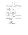
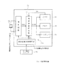
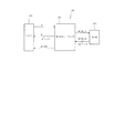
以下、本発明をマイクロコンピュータに適用した場合の第1実施例について図1乃至図4を参照して説明する。図1は、マイクロコンピュータ(マイコン)1の電気的構成を示す機能ブロック図である。マイコン1は、CPU2を中心として構成され、そのCPU2には、メインクロック発振部(発振回路)3によって発振出力されるメインクロック信号MCLK(例えば、周波数4MHz,第1クロック信号)が動作用クロック信号として供給されるようになっている。メインクロック発振部3は、具体的には図示しないが、水晶発振子を用いて構成されている。
(First embodiment)
A first embodiment when the present invention is applied to a microcomputer will be described below with reference to FIGS. FIG. 1 is a functional block diagram showing an electrical configuration of a
また、マイコン1は、CR発振回路で構成されるサブクロック発振部(CR発振回路)4を備えている。サブクロック発振部4によって発振出力されるサブクロック信号SCLK(例えば、周波数25kHz,第2クロック信号)は、ウォッチドッグタイマ5にカウント用クロック信号として供給されるようになっている。
ウォッチドッグタイマ5は、周知のようにCPU2の暴走監視機能をなすものであり、CPU2によって周期的なクリア動作が実行されなくなるとオーバーフローしてCPU2にリセット信号を出力する。また、本実施例におけるウォッチドッグタイマ5は、クリア動作画行なわれる時点でタイマ5のカウント値画家現地を超えていない場合にもリセット信号を出力するように構成されている。
In addition, the
As is well known, the
サブクロック補正部(補正回路)6は、メインクロック信号MCLKを用いてサブクロック信号SCLKの発振周波数補正を行なうように構成されている。一方、メインクロック監視部(監視回路)7は、サブクロック信号SCLKを用いてメインクロック信号MCLKの監視を行なうように構成されており、メインクロック信号MCLKの異常を検出すると、CPU2にリセット信号を出力するようになっている。
The sub clock correction unit (correction circuit) 6 is configured to correct the oscillation frequency of the sub clock signal SCLK using the main clock signal MCLK. On the other hand, the main clock monitoring unit (monitoring circuit) 7 is configured to monitor the main clock signal MCLK using the sub clock signal SCLK. When an abnormality in the main clock signal MCLK is detected, a reset signal is sent to the
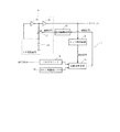
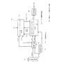
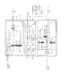
図2は、サブクロック補正部6を中心とする詳細な構成を示すものである。サブクロック補正部6は、エッジ検出回路8、パルスカウンタ9、カウント数設定レジスタ10、比較調整手段11および抵抗調整回路12を備えている。また、サブクロック発振部4は、抵抗調整回路6からの制御信号により抵抗値が可変な可変抵抗器としてのラダー抵抗13、コンデンサ14、インバータ15およびバッファ16で構成されている。
FIG. 2 shows a detailed configuration centering on the
サブクロック補正部6のエッジ検出回路8は、サブクロック発振部4からの発振出力のエッジを検出して検出信号を生成する。パルスカウンタ9は、メインクロック信号MCLKの出力パルスを計数するデジタルカウンタである。また、カウント数設定レジスタ10は、サブクロック信号SCLKの一周期に相当すべきMCLKパルスの適正なカウント数が格納されるレジスタである。すなわち、カウント数設定レジスタ10に設定されるカウント数には、MCLKパルスがそのカウント数だけ発生する時間に応じて、サブクロック信号SCLKの発振周期が調整されるべき数値が設定される。
The
比較調整手段11は、エッジ検出回路8からエッジ検出信号を受け取ると、パルスカウンタ9によるパルスのカウント数とレジスタ4に格納されたカウント数とを比較し、両カウント数の比較結果に基づいて、サブクロック信号SCLKの発振周期を調整するための調整信号を出力するように構成されている。
抵抗調整回路12は、比較調整手段11からの調整信号に基づいて制御信号を生成し、この制御信号をもってサブクロック発振部4のラダー抵抗13の抵抗値を調整する回路である。
When receiving the edge detection signal from the
The
尚、サブクロック補正部6の動作については、特開2001−111389号公報に詳細に開示されているが、以下、その概略について述べる。サブクロック信号SCLKの一周期が経過して、そのクロックパルスのエッジがエッジ検出回路8によって検出されると、検出信号が比較調整手段11に出力される。すると、比較調整手段11は、パルスカウンタ9で積算されている前回の検出信号から積算されたパルスのカウント数と、カウント数設定レジスタ10に設定されているカウント数とを読み出して両者を比較する。
The operation of the
ここで、レジスタ10に設定されているカウント数は、サブクロック信号SCLKの一周期に相当すべきパルスの適正な積算値である。そこで、比較調整手段11は、MCLKパルスがサブクロック信号SCLKの一周期のうちにいくつ積算されたかをもって、サブクロック信号SCLKの一周期が適正な設定値よりもどの程度大きいかあるいは小さいかを判定することができる。比較調整手段11は、その判定結果に基づいて、サブクロック信号SCLKの発振周期を調整するための調整信号を生成し、抵抗調整回路12は、この調整信号に基づいて制御信号を生成出力してラダー抵抗13の抵抗値を調整する。尚、図3は、以上の補正処理を示すフローチャートである。
Here, the count number set in the
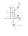
図4は、メインクロック監視部7の詳細な構成を示すものである。メインクロック監視部7は、Mカウンタ17及びSカウンタ18を中心として構成されている。Mカウンタ17は、1/N分周器19を介して与えられるメインクロック信号MCLKのパルスをカウントするカウンタであり、Sカウンタ18は、1/N分周器20を介して与えられるサブクロック信号SCLKのパルスをカウントするカウンタである。そして、Sカウンタ18は、Mカウンタ17におけるカウントデータのMSBが立つとリセットされると共に、リセットされずにオーバーフローするとCPU2にリセット信号を出力するように構成されている。
尚、1/N分周器19,20の分周値は、CPU2のプログラムによってセット可能に構成されている。また、分周器19,20については、クロック信号を分周することなくそのまま出力することも可能に構成されている。
FIG. 4 shows a detailed configuration of the main
The frequency division values of the 1 /
即ち、メインクロック監視部7においては、メインクロック信号MCLKの周波数が適正であれば、サブクロック信号SCLKの出力パルスをカウントするSカウンタ18がオーバーフローする前にMカウンタ17におけるカウントデータのMSBが立つことで、Sカウンタ18はリセットされるように設定されている。そして、メインクロック信号MCLKの周波数が低下した場合は、Mカウンタ17のMSBが立つ前にSカウンタ18がオーバーフローするので、CPU2はリセットされる。
That is, in the main
また、メインクロック監視部7におけるSカウンタ18のオーバーフロー周期は、ウォッチドッグタイマ5のオーバーフロー周期よりも短くなるように構成されている。
尚、メインクロック発振部3、サブクロック発振部4、サブクロック補正部6及びメインクロック監視部7は、クロック制御回路装置21を構成している。また、マイコン1としては、具体的には図示しないが、その他、ROM、RAMやI/O,A/D変換部などの周辺回路を備えている。
Further, the overflow cycle of the
The main
そして、クロック制御回路装置21のサブクロック補正部6及びメインクロック監視部7、並びにウォッチドッグタイマ5の機能を組み合わせることで、総合的に以下のような監視形態がとられることになる。
(1)MCLK:正常,SCLK:周波数低下
サブクロック補正部6の範囲内で補正され、その補正範囲を超える場合は、ウォッチドッグタイマ5によりCPU2にリセットがかかる。
(2)MCLK:正常,SCLK:周波数上昇
サブクロック補正部6の範囲内で補正され、その補正範囲を超える場合は、メインクロック監視部7によりCPU2にリセットがかかる。
(3)MCLK:周波数低下,SCLK:正常
相対的にSCLKが速くなることから、メインクロック監視部7によりCPU2にリセットがかかる。
(4)MCLK:周波数上昇,SCLK:正常
相対的にSCLKが遅くなることから、ウォッチドッグタイマ5によりCPU2にリセットがかかる。
Then, by combining the functions of the
(1) MCLK: Normal, SCLK: Frequency reduction If the correction is made within the range of the
(2) MCLK: Normal, SCLK: Increase in frequency When the correction is made within the range of the sub
(3) MCLK: Frequency reduction, SCLK: Normal Since the SCLK becomes relatively faster, the main
(4) MCLK: frequency increase, SCLK: normal Since the SCLK becomes relatively slow, the
以上のように構成された本実施例によれば、クロック制御回路装置21のサブクロック補正部6は、メインクロック信号MCLKに基づいてサブクロック信号SCLKの発振周波数を補正し、メインクロック監視部7は、サブクロック信号SCLKに基づいてメインクロック信号MCLKの発振状態を監視する。従って、メイン,サブの2つのクロック信号によって互いに補正,監視を行なうので、発振動作の信頼性を総合的に向上させることができる。
According to the present embodiment configured as described above, the sub
また、本実施例によれば、メインクロック監視部7によるメインクロック信号MCLKの監視を行なう周期は、ウォッチドッグタイマ5の周期よりも短くなるように設定される。従って、メインクロック監視部7は、ウォッチドッグタイマ5の監視周期では検出することができない異常の発生を検出することが可能となる。即ち、メインクロック信号MCLKが遅くなった場合は、ウォッチドッグタイマ5によるリセットがかかる前にメインクロック監視部7によってリセットをかけることができる。
そして、サブクロック信号SCLKを補正することで、CPU2は、設計通りにウォッチドッグタイマ5をリセットすることができる。
Further, according to the present embodiment, the cycle of monitoring the main clock signal MCLK by the main
Then, by correcting the sub clock signal SCLK, the
<以下は参考>
A.発振子を使用して第1クロック信号を発振する発振回路と、
前記第1クロック信号よりも低い周波数の第2クロック信号を発振し、その発振周波数が調整可能に構成されるCR発振回路と、
前記第1クロック信号に基づいて、前記第2クロック信号の発振周波数を補正する補正回路と、
前記第2クロック信号に基づいて、前記第1クロック信号の発振状態を監視する監視回路とを備えて構成されることを特徴とするクロック制御回路装置。
上記Aのクロック制御回路装置によれば、補正回路は、第1クロック信号に基づいて第2クロック信号の発振周波数を補正し、監視回路は、第2クロック信号に基づいて第1クロック信号の発振状態を監視する。即ち、第1,第2の2つのクロック信号によって互いに補正,監視を行なうので、発振動作の信頼性を向上させることができる。
<The following is for reference>
A. An oscillation circuit for oscillating the first clock signal using an oscillator;
A CR oscillation circuit configured to oscillate a second clock signal having a frequency lower than that of the first clock signal and to adjust the oscillation frequency;
A correction circuit for correcting an oscillation frequency of the second clock signal based on the first clock signal;
A clock control circuit device comprising: a monitoring circuit that monitors an oscillation state of the first clock signal based on the second clock signal.
According to the clock control circuit device of A, the correction circuit corrects the oscillation frequency of the second clock signal based on the first clock signal, and the monitoring circuit oscillates the first clock signal based on the second clock signal. Monitor status. That is, since correction and monitoring are performed with the first and second clock signals, the reliability of the oscillation operation can be improved.
B.上記A記載のクロック制御回路装置と、
前記第1クロック信号に基づいて生成される動作クロック信号が供給されるCPUと、
前記第2クロック信号に基づいて前記CPUの動作を監視するウォッチドッグタイマとを備え、
前記監視回路による第1クロック信号の監視を行なう周期は、前記ウォッチドッグタイマ周期よりも短くなるように構成されていることを特徴とするマイクロコンピュータ。
上記Bのマイクロコンピュータによれば、監視回路による第1クロック信号の監視を行なう周期は、ウォッチドッグタイマ周期よりも短くなるように設定される。従って、監視回路は、ウォッチドッグタイマの監視周期では検出することができない異常の発生を検出することが可能となる。
B. A clock control circuit device according to A above;
A CPU to which an operation clock signal generated based on the first clock signal is supplied;
A watchdog timer for monitoring the operation of the CPU based on the second clock signal,
The microcomputer is configured such that a period of monitoring the first clock signal by the monitoring circuit is shorter than the period of the watchdog timer.
According to the microcomputer B, the cycle for monitoring the first clock signal by the monitoring circuit is set to be shorter than the watchdog timer cycle. Therefore, the monitoring circuit can detect the occurrence of an abnormality that cannot be detected in the monitoring period of the watchdog timer.
(第2実施例)
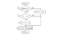
図5乃至図8は本発明の第2実施例を示すものであり、第1実施例と同一部分には同一符号を付して説明を省略以下異なる部分についてのみ説明する。第2実施例における構成は基本的に第1実施例と同様であり、比較調整手段11による調整動作が若干異なっている。
即ち、図5に示すフローチャートでは、ステップS3,S4の間に「CVに最大値をセット」の処理ステップS11が挿入されている。また、ステップS7,S8は、ステップS12,S13に置き換わっている。ここで、「CV」とは、比較調整手段11が出力する調整信号データである。
即ち、図5に示すフローチャートの実行が開始されるのは(スタート)、CPU2のリセットや、スリープモードなどの低消費電力モードが解除された場合の起動時である。その場合に、ステップS11において補正データの初期値が最大値(max)にセットされることになる。
(Second embodiment)
FIGS. 5 to 8 show a second embodiment of the present invention. The same parts as those in the first embodiment are designated by the same reference numerals, and the description thereof is omitted. Only different parts will be described below. The configuration of the second embodiment is basically the same as that of the first embodiment, and the adjustment operation by the comparison adjustment means 11 is slightly different.
That is, in the flowchart shown in FIG. 5, the processing step S11 of “set maximum value in CV” is inserted between steps S3 and S4. Steps S7 and S8 are replaced with steps S12 and S13. Here, “CV” is adjustment signal data output from the
That is, the execution of the flowchart shown in FIG. 5 is started (start) when the
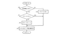
図6は、ステップS12における処理内容を示すものである。先ず、比較調整手段11は、高速補正を行なうか否かを判断する(ステップA0)。この設定はユーザによって行われるようになっており、例えばユーザプログラム中や、基板上に設けられたディップスイッチなどで設定される。高速補正を行うように設定されていない場合(「NO」)、比較調整手段11は、調整信号データCVを補正データの最小単位(LSB)に設定し(ステップA4)、それからステップA3に移行する。この場合は、補正が最小単位で行なわれるため、第1実施例と同様の低速補正となる。ステップA3では、調整信号データCVを抵抗調整回路12に出力することで、データCVに応じてラダー抵抗13の抵抗値を増加させる。
FIG. 6 shows the processing contents in step S12. First, the comparison /
一方、ステップA0において、高速補正を行うように設定されている場合(「YES」)、比較調整手段11は、調整信号データCVがその時点で最小単位になっているか否かを判断する(ステップA1)。そして、データCVが最小単位に等しければ(「YES」)ステップA3に移行する。
また、ステップA1において、データCVが最小単位に等しくなければ(「NO」)、比較調整手段11は、調整信号データCVを1/2にしてから(ステップA2)ステップA3に移行する。尚、図7に示すステップS13における処理では、ステップA3’の処理が、ステップA3の「増加」を「減少」に変更したものである。
On the other hand, if it is set in step A0 to perform high-speed correction (“YES”), the comparison /
In step A1, if the data CV is not equal to the minimum unit (“NO”), the comparison /
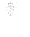
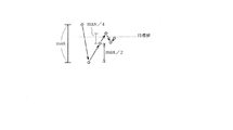
ここで、図8には、高速補正動作が行なわれる状態(即ち、ステップS12についてはステップA3を実行する場合)の概念的な説明図を示す。即ち、最初の補正は調整範囲の最大値maxによって行なわれ、例えば、サブクロック信号SCLKの周期データがレジスタ10の設定値よりも大きい(周波数が低い)場合は、周期が短くなる方向に最大値maxで振る。
その次の補正では、周期が短くなったため、周期が長くなる方向に最大値maxの1/2で振る。更に、その次の補正では周期が未だ短いため、更に周期が長くなる方向にmax/4で振る。すると、今度は目標値を超えたため、次の補正では周期が長くなる方向にmax/8で振るようにする。
Here, FIG. 8 shows a conceptual explanatory diagram of a state in which the high-speed correction operation is performed (that is, when step A3 is executed for step S12). That is, the first correction is performed based on the maximum value max of the adjustment range. For example, when the period data of the sub clock signal SCLK is larger than the set value of the register 10 (frequency is low), the maximum value is set in the direction in which the period becomes shorter. Shake at max.
In the next correction, since the cycle is shortened, it is shaken at a half of the maximum value max in the direction in which the cycle becomes longer. Further, in the next correction, since the cycle is still short, it is shaken at max / 4 in a direction in which the cycle becomes longer. Then, since the target value has been exceeded this time, the next correction is performed with max / 8 in a direction in which the cycle becomes longer.
以上のように、最大値maxで補正を開始して、絶対値が1/2,1/4,1/8と漸減していくように補正を行なう。即ち、データ検索方式でいえば、所謂バイナリサーチを同じ概念である。即ち、CPU2のリセット解除時や、低消費電力モードから通常モードに移行した場合のような起動時には、サブクロック発振部4の発振状態はかなり不安定となり、その発振周波数は、設定された周波数から大きく外れた状態にあると推定される。従って、その期間における調整動作についてはバイナリサーチ方式で行うことで、サブクロック信号SCLKの周期データがより速くレジスタ10の設定値に等しくなるように(狙い周波数に収束するように)補正される。
そして、調整信号データCVを1/2にすることを繰り返すと、最終的にはデータの最小値(LSB)に到達する(ステップA1,「YES」)。それ以降は、その最小値によって補正が継続されることになる。
As described above, correction is started at the maximum value max, and correction is performed so that the absolute value gradually decreases to 1/2, 1/4, and 1/8. That is, in terms of the data search method, so-called binary search is the same concept. That is, when the
When the adjustment signal data CV is repeatedly halved, the data reaches the minimum value (LSB) (step A1, “YES”). Thereafter, the correction is continued with the minimum value.
また、ステップA0において、高速補正を行なうか否かを選択可能としたのは、以下の理由による。即ち、CPU2が低消費電力モードを実行可能に構成されている場合、高速補正を行なっている途中で低消費電力モードに移行すると、サブクロック発振部4の発振周波数が設定周波数と大きく離れた状態のままで移行してしまうおそれがある。従って、低消費電力モードへの移行周期の設定に応じて調整方式を選択することで、ユーザの設計意図に応じた調整が可能となる。
In step A0, it is possible to select whether to perform high-speed correction for the following reason. That is, when the
以上のように第2実施例によれば、サブクロック補正部6の比較調整手段11は、CPU2が起動した直後に、サブクロック発振部4の発振周波数を調整する場合は、調整範囲の最大値より開始して、その絶対値を調整周期毎に1/2ずつ減少させるようにした。従って、サブクロック信号SCLKの周波数を、設定周波数により速く収束させることが可能となる。
そして、比較調整手段11は、調整信号レベルの絶対値が最小値(LSB)に達すると以降はその最小値によって調整を継続するので、発振周波数が設定周波数の近傍に近付いた状態になれば調整を精密に行なうことが可能となる。更に、比較調整手段11は、CPU2が起動した直後の調整動作においては、高速補正を行なうか否かを選択可能とするので、ユーザの意図に沿うように調整を行なわせることができる。
As described above, according to the second embodiment, the comparison /
Then, when the absolute value of the adjustment signal level reaches the minimum value (LSB), the comparison /
<以下は参考>
C.発振子を使用して第1クロック信号を発振する発振回路と、
前記第1クロック信号に基づいて生成される動作クロック信号が供給されるCPUと、
前記第1クロック信号よりも低い周波数の第2クロック信号を発振し、その発振周波数が調整可能に構成されるCR発振回路と、
前記第1クロック信号に基づいて、前記第2クロック信号の発振周波数を補正する補正回路とを備え、
前記補正回路は、前記第2クロック信号のエッジを検出するエッジ検出回路と、前記第1クロック信号に基づいてカウント動作を行なうパルスカウンタと、前記第2クロック信号の一周期に相当すべき前記パルスカウンタのカウント数が格納されるカウント数設定レジスタと、前記エッジ検出回路からエッジ検出信号を受け取ると、前記パルスカウンタのカウント数と前記カウント数設定レジスタに格納されたカウント数とを比較し、両者の差に基づいて前記CR発振回路の発振周波数を調整するための調整信号を生成する比較調整手段と、前記調整信号に基づいて、前記CR発振回路の発振周波数を調整する調整回路とを備えて構成され、
前記比較調整手段は、前記CPUが起動した直後の調整動作においては、前記調整信号レベルの絶対値を調整周期毎に漸減させるように構成されていることを特徴とするマイクロコンピュータ。
<The following is for reference>
C. An oscillation circuit for oscillating the first clock signal using an oscillator;
A CPU to which an operation clock signal generated based on the first clock signal is supplied;
A CR oscillation circuit configured to oscillate a second clock signal having a frequency lower than that of the first clock signal and to adjust the oscillation frequency;
A correction circuit for correcting an oscillation frequency of the second clock signal based on the first clock signal;
The correction circuit includes an edge detection circuit that detects an edge of the second clock signal, a pulse counter that performs a counting operation based on the first clock signal, and the pulse that should correspond to one cycle of the second clock signal. When a count number setting register for storing the count number of the counter and an edge detection signal is received from the edge detection circuit, the count number of the pulse counter is compared with the count number stored in the count number setting register. Comparison adjusting means for generating an adjustment signal for adjusting the oscillation frequency of the CR oscillation circuit based on the difference between the two, and an adjustment circuit for adjusting the oscillation frequency of the CR oscillation circuit based on the adjustment signal. Configured,
The microcomputer is configured to gradually decrease the absolute value of the adjustment signal level every adjustment cycle in the adjustment operation immediately after the CPU is activated.
上記Cのマイクロコンピュータによれば、比較調整手段は、CPUが起動した直後に、CR発振回路の発振周波数を調整する場合は、調整信号レベルの絶対値を調整周期毎に漸減させる。即ち、CPUのリセット解除時や、低消費電力モードから通常モードに移行した場合のような起動時には、CR発振回路の発振状態はかなり不安定となり、その発振周波数は、設定された周波数から大きく外れた状態にあると推定される。従って、その期間における調整動作については、調整信号レベルの絶対値を、調整周期毎に大きな値から小さな値に漸減させるように調整を行なえば、設定周波数により速く収束させることが可能となる。 According to the microcomputer C, when the oscillation frequency of the CR oscillation circuit is adjusted immediately after the CPU is activated, the comparison adjustment unit gradually decreases the absolute value of the adjustment signal level every adjustment cycle. In other words, when the CPU is released from reset or started up, such as when shifting from the low power consumption mode to the normal mode, the oscillation state of the CR oscillation circuit becomes considerably unstable, and the oscillation frequency deviates significantly from the set frequency. Estimated to be in the state. Accordingly, the adjustment operation during that period can be converged more quickly with the set frequency if the adjustment signal level is adjusted so that the absolute value of the adjustment signal level is gradually decreased from a large value to a small value every adjustment cycle.
D.前記比較調整手段は、前記調整動作においては、調整範囲の最大値より開始して、その絶対値を調整周期毎に1/2ずつ減少させることを特徴とする上記Cのマイクロコンピュータ。
上記Dのマイクロコンピュータによれば、比較調整手段は、調整動作においては、調整範囲の最大値より開始して、その絶対値を調整周期毎に1/2ずつ減少させる。即ち、データ検索における所謂バイナリサーチと同様の方式によることで、CR発振回路の発振周波数を設定周波数により速く収束させることが可能となる。
D. The microcomputer according to the above C, wherein, in the adjustment operation, the comparison adjustment means starts from the maximum value of the adjustment range and decreases the absolute value by ½ every adjustment period.
According to the microcomputer D, in the adjustment operation, the comparison adjustment means starts from the maximum value of the adjustment range and decreases the absolute value by ½ every adjustment cycle. That is, by using the same method as the so-called binary search in the data search, the oscillation frequency of the CR oscillation circuit can be converged faster by the set frequency.
E.前記比較調整手段は、前記調整信号レベルの絶対値が最小値に達すると、以降はその最小値によって調整を継続することを特徴とする上記CまたはDのマイクロコンピュータ。
上記Eのマイクロコンピュータによれば、比較調整手段は、調整信号レベルの絶対値が最小値に達すると以降はその最小値によって調整を継続するので、発振周波数が設定周波数の近傍に近付いた状態になれば調整を精密に行なうことが可能となる。
E. The microcomputer according to the above C or D, wherein when the absolute value of the adjustment signal level reaches a minimum value, the comparison / adjustment means continues adjustment with the minimum value thereafter.
According to the microcomputer E described above, the comparison adjustment means continues the adjustment with the minimum value after the absolute value of the adjustment signal level reaches the minimum value, so that the oscillation frequency approaches the set frequency. If it becomes, it will become possible to adjust precisely.
F.前記比較調整手段は、前記CPUが起動した直後の調整動作においては、前記調整信号レベルの絶対値を調整周期毎に漸減させる調整動作を行なうか否かを選択可能に構成されていることを特徴とする上記C〜Eの何れかのマイクロコンピュータ。
上記Fのマイクロコンピュータによれば、比較調整手段は、CPUが起動した直後の調整動作においては、調整信号レベルの絶対値を調整周期毎に漸減させる調整動作を行なうか否かを選択可能に構成される。即ち、CPUが低消費電力モードを実行可能に構成されている場合、調整周期毎に漸減させる調整動作を行なっている途中で低消費電力モードに移行すると、CR発振回路の発振周波数が設定周波数と大きく離れた状態のままで移行してしまうおそれがある。従って、低消費電力モードへの移行周期の設定に応じて調整方式を選択できるようにすれば、ユーザの意図に沿うように調整を行なわせることができる。
F. The comparison adjustment means is configured to be able to select whether or not to perform an adjustment operation for gradually decreasing the absolute value of the adjustment signal level every adjustment cycle in the adjustment operation immediately after the CPU is started. The microcomputer according to any one of the above C to E.
According to the microcomputer F, the comparison and adjustment means can select whether or not to perform an adjustment operation for gradually decreasing the absolute value of the adjustment signal level every adjustment cycle in the adjustment operation immediately after the CPU is started. Is done. That is, when the CPU is configured to be able to execute the low power consumption mode, if the CPU shifts to the low power consumption mode during the adjustment operation for gradually decreasing every adjustment cycle, the oscillation frequency of the CR oscillation circuit becomes the set frequency. There is a risk of shifting in a state of being far away. Accordingly, if the adjustment method can be selected according to the setting of the transition period to the low power consumption mode, the adjustment can be performed in accordance with the user's intention.
C’.発振子を使用して第1クロック信号を発振する発振回路と、前記第1クロック信号に基づいて生成される動作クロック信号が供給されるCPUと、前記第1クロック信号よりも低い周波数の第2クロック信号を発振し、その発振周波数が調整可能に構成されるCR発振回路と、前記第1クロック信号に基づいて、前記第2クロック信号の発振周波数を補正する補正回路とを備えて構成されるマイクロコンピュータについて、前記第2クロック信号の発振周波数を調整する発振周波数の調整方法であって、
前記補正回路は、前記第2クロック信号のエッジを検出し、前記第1クロック信号に基づいてカウント動作を行ない、前記第2クロック信号の一周期に相当すべきカウント数を保持し、前記エッジ検出信号を受け取ると、前記カウント動作によって示されるカウント数と前記保持されたカウント数とを比較し、両者の差に基づいて前記CR発振回路の発振周波数を調整するための調整信号を生成し、前記調整信号に基づいて、前記CR発振回路の発振周波数を調整し、
前記CPUが起動した直後の調整動作においては、前記調整信号レベルの絶対値を調整周期毎に漸減させることを特徴とするクロック信号の発振周波数調整方法。
C '. An oscillation circuit that oscillates a first clock signal using an oscillator, a CPU to which an operation clock signal generated based on the first clock signal is supplied, and a second having a frequency lower than that of the first clock signal A CR oscillation circuit configured to oscillate a clock signal and its oscillation frequency is adjustable, and a correction circuit that corrects the oscillation frequency of the second clock signal based on the first clock signal. An oscillation frequency adjusting method for adjusting an oscillation frequency of the second clock signal for a microcomputer,
The correction circuit detects an edge of the second clock signal, performs a counting operation based on the first clock signal, holds a count number corresponding to one cycle of the second clock signal, and detects the edge When the signal is received, the count number indicated by the count operation is compared with the held count number, and an adjustment signal for adjusting the oscillation frequency of the CR oscillation circuit based on the difference between the two is generated, Based on the adjustment signal, the oscillation frequency of the CR oscillation circuit is adjusted,
In the adjustment operation immediately after the CPU is started, the absolute value of the adjustment signal level is gradually decreased every adjustment cycle.
D’.前記調整動作においては、調整範囲の最大値より開始して、その絶対値を調整周期毎に1/2ずつ減少させることを特徴とする上記C’のクロック信号の発振周波数調整方法。
E’.前記調整信号レベルの絶対値が最小値に達すると、以降はその最小値によって調整を継続することを特徴とする上記C’またはD’のクロック信号の発振周波数調整方法。
F’.前記CPUが起動した直後の調整動作においては、前記調整信号レベルの絶対値を調整周期毎に漸減させる調整動作を行なうか否かが選択可能であることを特徴とするC’〜E’のクロック信号の発振周波数調整方法。
D '. The method for adjusting the oscillation frequency of the clock signal C ′ described above, wherein the adjustment operation starts from the maximum value of the adjustment range and decreases the absolute value by ½ every adjustment cycle.
E '. When the absolute value of the adjustment signal level reaches a minimum value, the adjustment is continued with the minimum value thereafter, and the oscillation frequency adjustment method for the C ′ or D ′ clock signal is characterized.
F '. In the adjustment operation immediately after the CPU is activated, it is possible to select whether or not to perform an adjustment operation for gradually decreasing the absolute value of the adjustment signal level every adjustment cycle. Signal oscillation frequency adjustment method.
(第3実施例)
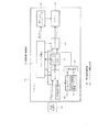
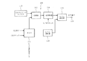
図9乃至図13は本発明の第3実施例を示すものである。図9は、マイクロコンピュータ(マイコン)31の構成を示す機能ブロック図である。マイコン31は、CPU32を中心として構成されている。そのCPU32には、クロック生成回路33より生成出力されるクロック信号が動作用クロック信号として供給されるようになっている。また、前記クロック信号は、その他周辺回路などの機能ブロック34にも供給されている。
(Third embodiment)
9 to 13 show a third embodiment of the present invention. FIG. 9 is a functional block diagram showing the configuration of the
低消費電力制御部(端子制御手段)35は、CPU32によって与えられる制御コマンドに応じて所謂スリープ/ストップモードなどの低消費電力モードに関する制御を行うものである。ここで、スリープモードとは、クロック生成回路33の動作を停止させることでCPU32に対する動作用クロック信号の供給を停止させ、CPU32は、内部レジスタのデータ値などを保持した状態で処理を一時的に停止するモードである。スリープモードは、設定された時間間隔で周期的に解除(ウェイクアップ)されるようになっている。
一方、ストップモードは、CPU32が処理を停止する点についてはストップモードと同様であるが、周期的に解除されることはなく、CPU32が処理すべき何らかのイベントが発生した場合にのみ解除されるモードである。
The low power consumption control unit (terminal control means) 35 performs control related to a low power consumption mode such as a so-called sleep / stop mode in accordance with a control command given by the
On the other hand, the stop mode is the same as the stop mode in that the
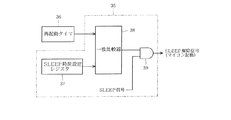
図10は、低消費電力制御部35が、スリープモードについて制御を行う機能部分の構成を示すものである。即ち、低消費電力制御部35は、例えばCR発振回路で構成される再起動タイマ36のカウント値と、内部のSLEEP時間設定レジスタ37の設定データ値とを一致比較器38によって比較し、両者が一致するとハイレベルの一致信号をANDゲート39の一方の入力端子に出力する。ANDゲート39の他方の入力端子には、SLEEP信号が与えられる。
従って、ハイレベルのSLEEP信号が与えられている期間において一致比較器38が一致信号を出力すると、ANDゲート39はハイレベルのSLEEP解除信号を出力する。この時、再起動タイマ36はリセットされる。
FIG. 10 shows a configuration of a functional part in which the low power
Therefore, when the
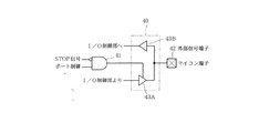
一方、図11は、低消費電力制御部35が、ストップモードが設定された場合にI/O端子部40の制御を行う機能部分の構成を示すものである。即ち、低消費電力制御部35のANDゲート41の負論理入力端子と正論理入力端子には、夫々STOP信号,ポート制御信号が与えられるようになっている。そして、ANDゲート41はI/O端子部40にハイインピーダンス制御信号を出力する。
I/O端子部40は、入出力端子(外部信号端子)42にバッファ43A,43Bが双方向接続された構成である。そして、出力バッファ43Aは、ANDゲート41によって出力されるハイインピーダンス制御信号によって制御される。また、I/O端子部40は、I/O制御部44によって入出力切替え制御(ポート制御)と出力レベル制御が行われるようになっている。前記ポート制御信号は、I/O制御部44によって出力される。
On the other hand, FIG. 11 shows a configuration of a functional part in which the low power
The I /
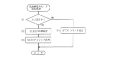
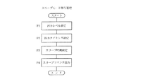
次に、第3実施例の作用について図12及び図13を参照して説明する。図12は、CPU32が低消費電力モードに移行する場合の処理を示すフローチャートである。CPU32は、低消費電力モードが「スリープ」であるか否かを判断する(ステップB1)。そして、「スリープ」である場合は(「YES」)、SLEEP時間設定レジスタ37にスリープモードの移行期間データを設定する(ステップB2)。それから、低消費電力制御部35に対してSLEEPコマンドを出力すると(ステップB3)処理を終了する。この場合、低消費電力制御部35の図9に示す構成部分がアクティブとなり、スリープモードの移行期間の計測が開始され、その期間が終了するとスリープモードは解除される。
Next, the operation of the third embodiment will be described with reference to FIGS. FIG. 12 is a flowchart illustrating processing when the
一方、低消費電力モードが「ストップ」である場合(ステップB1,「NO」)、CPU32は、低消費電力制御部35に対してSTOPコマンドを出力する(ステップB4)。そして、処理を終了する。この場合、低消費電力制御部35の図11に示す構成部分が作用する。即ち、STOP信号がハイレベルとなり、ANDゲート41の出力レベルはロウとなることで、出力バッファ43Aの出力端子はハイインピーダンス状態となる。
On the other hand, when the low power consumption mode is “stop” (step B1, “NO”), the
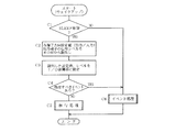
また、図13は、低消費電力モードが解除されて、CPU32が起動(ウェイクアップ)する場合の処理を示すフローチャートである。CPU32は、解除されたのがスリープモードか否かを判断し(ステップC1)、スリープモードであれば(「YES」)、その時点における各端子の方向(入力/出力)設定値、及び出力端子の信号レベル設定を、データとして保持しているROM(図示せず)などから読み出す(ステップC2)。そして、読み出した設定値やレベルの設定をI/O制御部44に再設定することで、各入出力端子42等における出力信号レベルを再設定する(ステップC3)。
FIG. 13 is a flowchart showing processing when the
それから、その時点で他に処理すべきイベントが発生しているか否かを判断し(ステップC4)、発生していれば(「YES」)そのイベントの処理を行なった後(ステップC6)、図12に示した低消費電力モードへの移行処理を行なう(ステップC5)。一方、ステップC4において処理すべきイベントが発生していなければ(「NO」)、そのままステップC5に移行する。 Then, it is determined whether another event to be processed has occurred at that time (step C4). If it has occurred ("YES"), the event is processed (step C6). Transition processing to the low power consumption mode shown in FIG. 12 is performed (step C5). On the other hand, if an event to be processed has not occurred in step C4 ("NO"), the process proceeds to step C5 as it is.
以上のように第3実施例によれば、マイコン31のCPU32は、スリープモードが再起動タイマ36によって周期的に解除される毎に、入出力端子42の信号出力レベルを再設定してからスリープモードに移行するようにした。従って、CPU32が、たとえ、スリープモード移行中に外来ノイズの影響を受けることで入出力端子42の信号出力レベルが変化したとしても、その出力レベルはスリープモードが周期的に解除される毎に再設定されるので、マイコン31の信頼性を向上させることができる。
As described above, according to the third embodiment, the
また、マイコン31の低消費電力制御部35は、CPU32が低消費電力モードに移行する場合、入出力端子42をハイインピーダンス状態に設定するようにした。従って、CPU32が、例え、ストップモードの移行中に上述と同様に外来ノイズの影響を受けたとしても、入出力端子42がハイインピーダンス状態であるから、その端子42によってマイコン31に接続されている外部デバイスが駆動されることはなく、信頼性を向上させることができる。
Further, the low power
(第4実施例)
図14乃至図17は本発明の第4実施例を示すものである。図14は、マイクロコンピュータ51のクロック制御に関する機能部分を示すブロック図である。マイコン51は、CPU52を中心として構成されている。そのCPU52は、セレクタ53を介して動作用クロック(マシンクロック)信号が選択的に与えられるようになっている。
セレクタ53には、マイコン51に外付けされる外部発振子54による原発振信号と、DPLL(Digital Phase Locked Loop)回路55によって出力される逓倍クロック信号とが与えられている。そして、セレクタ53の切替えは、クロック制御部(切替通知制御部)56によって行われるようになっている。
(Fourth embodiment)
14 to 17 show a fourth embodiment of the present invention. FIG. 14 is a block diagram showing functional parts related to clock control of the
The
また、DPLL回路(周波数逓倍回路)55の基準クロック信号もセレクタ57を介して与えられるようになっており、そのセレクタ57には、外部発振子54による原発振信号と、CR発振回路58によって出力されるCRクロック信号とが与えられている。そして、セレクタ57の切替えもクロック制御部56によって行われるようになっている。例えば、原発振信号は周波数4MHz,CRクロック信号は周波数25kHzである。尚、クロック制御部56は、CRクロック信号をDPLL回路55のクロックソースとして選択する場合は、外部発振子54の発振動作を停止させるように構成されている。
The reference clock signal of the DPLL circuit (frequency multiplication circuit) 55 is also supplied via the
CRクロック信号は、CRカウンタ59にもカウント用クロックとして与えられている。一致比較部60には、CRカウンタ59のカウントデータと、発振安定時間設定レジスタ61の設定データが与えられている。その設定データは、電源投入時にはハードウエアによって初期値がセットされるが、CPU52が実行するユーザプログラムによってもセット可能となっている。一致比較部60は、両者のデータ値を比較して一致すると、一致信号をクロック制御部56に出力するようになっている。
The CR clock signal is also supplied to the
即ち、設定レジスタ61に、外部発振子54の発振安定時間に相当するデータをセットすれば、前記一致信号が出力されるタイミングによってその発振安定時間の経過が判る。また、クロック制御部56は、DPLL回路55が内蔵しており内部の発振動作シーケンスを制御するために用いられるステートカウンタ(シーケンス制御手段)62のカウンタ値を参照することで、DPLL回路55の発振安定時間の経過を知ることも可能となっている。
That is, if data corresponding to the oscillation stabilization time of the
尚、ここでのステートカウンタ62は、例えば第5実施例における制御回路20と同様のものであり、例えば、外部発振子54の出力クロックを基準クロック信号とする場合、その8カウントを1制御周期とするようになっている。従って、逓倍動作開始時においては、その1制御周期が経過した時点で最初の演算結果としての逓倍クロック信号が出力されることになり、その期間が発振安定期間となる。
Here, the
そして、クロック制御部56は、それらの検出タイミングにおいて、CPU52の割り込みコントローラ63にクロック切替え完了割り込み信号を出力するようになっている。割り込みコントローラ63は、その他の割り込み要因も含めてイネーブル制御やマスク制御などを行い、適切な割り込み信号をCPU52に出力するようになっている。
Then, the clock controller 56 outputs a clock switching completion interrupt signal to the interrupt
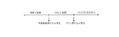
次に、第4実施例の作用について図15乃至図17も参照して説明する。図15は、電源投入時や、スリープ/ストップモードからCPU52が起動したウェイクアップ時におけるクロック信号の遷移状態を示すものである。即ち、スリープ/ストップモードに遷移した場合は、CR発振回路58を除いてクロック信号の発振動作は停止される。先ず、外部発振子54が電源投入によって発振動作を開始する。発振開始の初期においてはその発振動作即ち発振周波数が不安定であるから、CPU52はDPLL回路55の動作を禁止している。
Next, the operation of the fourth embodiment will be described with reference to FIGS. FIG. 15 shows the transition state of the clock signal when the power is turned on or when the
そして、CRカウンタ59のカウンタ値が発振安定時間設定レジスタ61の設定データに一致し、一致比較部60が一致信号をクロック制御部56に出力すると、クロック制御部56は、それを受けて割り込み信号を、割り込みコントローラ63を介してCPU52に出力する。すると、CPU52は、その割り込み信号によって外部発振子54の発振動作が安定したことを認識し、DPLL回路55に周波数逓倍動作を開始させる。
そして、クロック制御部56は、今度はDPLL回路55のステートカウンタ62のカウンタ値を参照し、DPLL回路55の動作が安定するまで待機し、動作が安定した状態になった時点で割り込み信号を出力する。従って、CPU52はその割り込みによってDPLL回路55の動作が安定したことを認識できる。
When the counter value of the CR counter 59 matches the set data of the oscillation stabilization
The clock control unit 56 then refers to the counter value of the
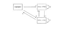
また、図16は、CPU52が通常の動作を行なっている状態において、ユーザプログラムによりマシンクロックの切替を行なう場合のダイヤグラムである。この場合、クロックソースとしては、外部発振子54,DPLL回路55(外部発振子54がソース),DPLL回路55(CR発振回路58がソース)の3種類があり、これらの間でクロック信号の選択切替が行なわれる。また、DPLL回路55は、CPU52が逓倍又は分周データを設定することでクロックソースの周波数を逓倍または分周可能であるから、DPLL回路55単体においても周波数切替が行なわれる。これらのパターンを下記に示す。
A: 外部発振子→DPLL回路(外部ソース)
B: 外部発振子→DPLL回路(CRソース)
C:DPLL回路(外部ソース)→DPLL回路(CRソース)
D:DPLL回路(CRソース)→外部発振子
E:DPLL回路(CRソース)→DPLL回路(外部ソース)
X:DPLL回路における周波数変更
FIG. 16 is a diagram when the machine clock is switched by the user program in a state where the
A: External oscillator → DPLL circuit (external source)
B: External oscillator → DPLL circuit (CR source)
C: DPLL circuit (external source) → DPLL circuit (CR source)
D: DPLL circuit (CR source) → external oscillator E: DPLL circuit (CR source) → DPLL circuit (external source)
X: Frequency change in DPLL circuit
図17は、CPU52が、図16に示すダイヤグラムに基づいてマシンクロック信号の切替を行なう場合の処理を示すフローチャートである。CPU52は、先ず、クロック信号の切替えパターンを上記A〜E,Xの中から選択する(ステップD1)。そして、パターンD,Eであれば(ステップD2,「YES」)、外部発振子54の発振安定時間データを設定レジスタ61にセットし(ステップD3)、パターンに応じたクロック切替を行なう(ステップD4)。
クロック切替は、CPU52がクロック制御部56の内部にある設定レジスタにデータを書き込むことで、セレクタ53,57を切替えて行なう。また、ステップD2において切替えパターンがD,E以外であれば(「NO」)、そのままステップD4に移行する。
FIG. 17 is a flowchart showing processing when the
The clock switching is performed by switching the
続いて、CPU52は、ステップD2と同様に切替えパターンがD,Eか否かを判断し(ステップD5)、パターンD,Eであれば(「YES」)外部発振割り込みが発生するまで待機する(ステップD6)。そして、割り込みが発生すると(「YES」)ステップD7に移行する。また、ステップD5においてパターンD,E以外の場合もステップD7に移行する。
Subsequently, the
ステップD7において、CPU52は、切替えパターンDか否かを判断し、パターンDでなければ(「NO」)PLL割り込みが発生するのを待って(ステップD8,「YES」)処理を終了する。また、ステップD7においてパターンDであれば(「YES」)そのまま処理を終了する。即ち、CPU52は、パターンEの場合は外部発振割り込み,PLL割り込み双方の発生を待つことでクロック安定を認識する。パターンDの場合は外部発振割り込みのみ、その他のパターンではPLL割り込みのみの発生を待つことでクロック安定を認識することになる。
In step D7, the
以上のように第4実施例によれば、マイコン51のクロック制御部56は、DPLL回路55の発振動作をステートカウンタ62によって監視し、逓倍クロック信号の周波数が切替えられた場合は、その切替えに伴う発振動作が安定したタイミングでCPU52に対して割り込み要求を発生させるようにした。
従って、CPU52は、冗長な待機時間を設定する必要がなくなり、処理効率を向上させることができる。そして、クロック制御部56は、シーケンスカウンタ62を参照することでDPLL回路55の発振動作が安定したことを明確に認識することができる。
As described above, according to the fourth embodiment, the clock control unit 56 of the
Therefore, the
また、CPU52の動作用クロック信号を、セレクタ53,57によって複数のクロック信号の内から選択可能としたので、より多様なクロック信号を選択することによって、制御範囲を広げることができる。
そして、クロック制御部56は、外部発振子54の発振動作も監視し、その動作切替えに伴う発振動作が安定したタイミングでもCPU52に対して割り込み要求を発生させるので、CPU52は、その割り込み要求の発生によってDPLL回路55の動作を開始させるのに適切なタイミングを知ることが可能となる。
Further, since the operation clock signal of the
The clock control unit 56 also monitors the oscillation operation of the
<以下は参考>
G.基準クロック信号の周波数を逓倍して出力する周波数逓倍回路と、
この周波数逓倍回路によって出力される逓倍クロック信号が動作用クロック信号として供給可能であるCPUと、
前記周波数逓倍回路の発振動作を監視し、前記逓倍クロック信号の周波数が切替えられた場合は、その切替えに伴う発振動作が安定したタイミングで前記CPUに対して割り込み要求を発生させる切替通知制御部とを備えて構成されることを特徴とするマイクロコンピュータ。
上記Gのマイクロコンピュータによれば、切替通知制御部は、周波数逓倍回路の発振動作を監視し、逓倍クロック信号の周波数が切替えられた場合は、その切替えに伴う発振動作が安定したタイミングでCPUに対して割り込み要求を発生させる。従って、CPUは、逓倍クロック信号の周波数を切替えた場合に、その発振動作が安定したことを割り込みによって知ることができるので、冗長な待機時間を設定する必要がなくなり、処理効率を向上させることができる。
<The following is for reference>
G. A frequency multiplication circuit that multiplies and outputs the frequency of the reference clock signal;
A CPU capable of supplying a multiplied clock signal output by the frequency multiplication circuit as an operation clock signal;
A switching notification control unit that monitors the oscillation operation of the frequency multiplication circuit and, when the frequency of the multiplied clock signal is switched, generates an interrupt request to the CPU at a timing when the oscillation operation associated with the switching is stabilized; A microcomputer comprising:
According to the microcomputer G, the switching notification control unit monitors the oscillation operation of the frequency multiplying circuit, and when the frequency of the multiplied clock signal is switched, the switching notification control unit notifies the CPU at a timing when the oscillation operation accompanying the switching is stable. An interrupt request is generated. Therefore, when the frequency of the multiplied clock signal is switched, the CPU can know that the oscillation operation is stabilized by an interrupt, so that it is not necessary to set a redundant standby time, and the processing efficiency can be improved. it can.
H.前記周波数逓倍回路は、前記基準クロック信号に基づいて、発振動作シーケンスを制御するための制御信号を出力するシーケンス制御手段を備え、
前記切替通知制御部は、前記制御信号に基づいて前記周波数逓倍回路の発振動作を監視することを特徴とする上記Gのマイクロコンピュータ。
上記Hのマイクロコンピュータによれば、切替通知制御部は、周波数逓倍回路の発振動作シーケンスを制御するシーケンス制御手段によって出力される制御信号に基づいて、当該周波数逓倍回路の発振動作を監視するので、発振動作が安定したことを制御信号によって明確に認識することができる。
H. The frequency multiplication circuit includes sequence control means for outputting a control signal for controlling an oscillation operation sequence based on the reference clock signal,
The G microcomputer according to
According to the microcomputer of H, the switching notification control unit monitors the oscillation operation of the frequency multiplication circuit based on the control signal output by the sequence control means that controls the oscillation operation sequence of the frequency multiplication circuit. It can be clearly recognized by the control signal that the oscillation operation is stable.
I.前記動作用クロック信号として供給可能なクロック信号が、前記逓倍クロック信号の他にも1つ以上存在し、
前記動作用クロック信号は、それら複数のクロック信号の内から選択可能に構成されていることを特徴とする上記GまたはHのマイクロコンピュータ。
上記Iのマイクロコンピュータによれば、CPUの動作用クロック信号は、逓倍クロック信号を含む複数のクロック信号の内から選択可能に構成されるので、そのような構成においても上記Hと同様の作用効果を得ることができる。
I. There are one or more clock signals that can be supplied as the operation clock signal in addition to the multiplied clock signal.
The G or H microcomputer described above, wherein the operation clock signal can be selected from the plurality of clock signals.
According to the microcomputer I, the operation clock signal of the CPU is configured to be selectable from a plurality of clock signals including the multiplied clock signal. Can be obtained.
J.前記切替通知制御部は、前記動作用クロック信号として供給可能なクロック信号を出力する外部発振子の発振動作も監視し、その動作切替えに伴う発振動作が安定したタイミングでも前記CPUに対して割り込み要求を発生させることを特徴とする上記Iのマイクロコンピュータ。
上記Jのマイクロコンピュータによれば、切替通知制御部は、外部発振子の発振動作も監視し、その動作切替えに伴う発振動作が安定したタイミングでもCPUに対して割り込み要求を発生させる。従って、外部発振子によって出力されるクロック信号が周波数逓倍回路の基準クロック信号となる場合、CPUは、前記割り込み要求の発生によって周波数逓倍回路の動作を開始させるのに適切なタイミングを知ることが可能となる。
J. et al. The switching notification control unit also monitors the oscillation operation of an external oscillator that outputs a clock signal that can be supplied as the operation clock signal, and issues an interrupt request to the CPU even when the oscillation operation is stabilized due to the operation switching. A microcomputer according to the above I, characterized in that:
According to the microcomputer J, the switching notification control unit also monitors the oscillation operation of the external oscillator, and generates an interrupt request to the CPU even when the oscillation operation associated with the operation switching is stabilized. Therefore, when the clock signal output from the external oscillator becomes the reference clock signal of the frequency multiplication circuit, the CPU can know the appropriate timing for starting the operation of the frequency multiplication circuit by the generation of the interrupt request. It becomes.
(第5実施例)
図18乃至図23は、本発明を車両用ECU(Electronic Control Unit)に適用した場合の第5実施例を示すものである。尚、以下に述べる構成の基本的部分は特開2000−357947号公報に開示されているので、以下では概略的に説明する。図18は、ECU(マイクロコンピュータ)71の電気的構成を示す機能ブロック図である。ECU71は、半導体集積回路(IC)として構成されており、その内部回路として、CPU72,メモリ73及びゲートアレイ74などのクロック同期回路を有している。ECU71には、水晶発振子75に外付けされており、発振回路(基準クロック発振回路)76は、水晶発振子75にバイアスを与えて周波数16KHzの基準クロック信号PREF を出力するようになっている。
(5th Example)
18 to 23 show a fifth embodiment when the present invention is applied to a vehicle ECU (Electronic Control Unit). The basic portion of the configuration described below is disclosed in Japanese Patent Application Laid-Open No. 2000-357947, and will be briefly described below. FIG. 18 is a functional block diagram showing an electrical configuration of the ECU (microcomputer) 71. The
その基準クロック信号PREF は周波数逓倍回路77に与えられており、周波数逓倍回路77は、その基準クロック信号PREF を512逓倍した周波数8MHz逓倍クロック信号POUT を生成して、CPU72,メモリ73及びゲートアレイ74のクロック入力端子に出力するようになっている。周波数逓倍回路77は、所謂DPLL(Digital Phase Locked Loop)回路として構成されるものであり、前記逓倍数は、CPU72より与えられる逓倍数設定データDVの値に応じて設定される。
また、周波数逓倍回路77には、低消費電力制御回路(低消費電力制御手段)78によってECU71の動作モードを低消費電力モードとスタンバイモードとに切換えるためのモード制御信号PA(停止制御)が出力されるようになっている。
The reference clock signal PREF is supplied to a
Further, the
キー検出スイッチ79は、自動車のキーがキーシリンダ(何れも図示せず)に挿入されているか否かを検出するスイッチである。そして、キー検出スイッチ79がキー検出信号を低消費電力制御回路78に出力していなければ、低消費電力制御回路78は、モード制御信号PAをロウレベルにすることでECU71を低消費電力モード(スリープ/ストップ)に維持するようになっている。
また、キー検出スイッチ79がキー検出信号を出力した場合、低消費電力制御回路78は、モード制御信号PAをハイレベルにして、ECU71を低消費電力モードからスタンバイモードに切換える。尚、周波数逓倍回路77及び低消費電力制御回路78は、クロック制御回路(発振回路装置)71aを構成している。
The
When the
図19は、周波数逓倍回路77の概略構成を示す機能ブロック図である(尚、詳細な構成については、更に特開平8−265111号公報を参照)。制御回路(シーケンス制御手段)80には、発振回路76より出力される基準クロック信号PREF が与えられている。そして、制御回路80は、3個のフリップフロップ(図示せず)で構成されるシーケンスカウンタを内蔵している。
そして、このシーケンスカウンタによって基準クロック信号PREF の入力パルス数をカウントして基準クロック信号PREF の8周期を1シーケンス制御周期とし、基準クロック信号PREF に同期して各種の制御タイミング信号をDCO(Digital Controlled Oscillator ,デジタル制御発振器)81及びカウンタ・データラッチ回路82に出力する。
FIG. 19 is a functional block diagram showing a schematic configuration of the frequency multiplying circuit 77 (for further details, see Japanese Patent Laid-Open No. 8-265111). The control circuit (sequence control means) 80 is supplied with a reference clock signal PREF output from the
The sequence counter counts the number of input pulses of the reference clock signal PREF, and eight cycles of the reference clock signal PREF are set as one sequence control cycle. Various control timing signals are synchronized with the reference clock signal PREF by various control timing signals DCO (Digital Controlled). (Oscillator, digitally controlled oscillator) 81 and counter /
DCO81は、内部にリングオシレータ(多相クロック信号出力手段)83を備えている。リングオシレータ83は、図21に示すように、論理反転回路としてNANDゲート84と複数個のINV(インバータ)ゲート85とを備えて構成されている。これらのINVゲート84は、各出力端子が次段の入力端子へとリング状に接続されており、NANDゲート85の一方の入力端子は最終段のINVゲート(図示せず)の出力端子に接続され、他方の入力端子には外部からの停止制御信号が与えられている。そして、INVゲート84の各出力端子からは、夫々多相クロック信号R1〜R16が出力される。
The
再び、図19を参照して、カウンタ・データラッチ回路82には、制御回路80より出力される制御タイミング信号UCE及びCLRが与えられるようになっている。これらの制御タイミング信号UCE及びCLRは、基準クロック信号PREF 1周期に相当するパルス幅を有しており、制御回路80におけるシーケンス制御周期の第3及び第7周期に夫々出力される信号である。
Referring to FIG. 19 again, the counter /
また、カウンタ・データラッチ回路82には、リングオシレータ83より出力されるクロック信号R13がRCKとして与えられ、そのクロック信号RCKによって内部のアップカウンタ(16ビット)によるカウント動作を行う。そして、カウンタ・データラッチ回路82は、制御タイミング信号UCEが出力されている間、カウンタにアップカウント動作を行わせることで、基準クロック信号PREF 1周期に相当する時間をクロック信号RCKによってカウントする。
そのカウントデータは、制御回路80よりシーケンス制御周期の第5周期で出力される制御タイミング信号DLSがDCO81を介して与えられるラッチ信号DLCのタイミングでラッチされ、制御タイミング信号CLRが出力されるとラッチされたデータはクリアされる。
The counter /
The count data is latched when the control timing signal DLS output from the
カウンタ・データラッチ回路82は、カウントした16ビットのデータDT16〜DT1を、CPU72により与えられる逓倍数設定データDVに応じてデータビットを右シフトし、そのシフト後のデータの12ビットをラッチする。そして、ラッチされた12ビットのデータは、CD12〜CD1としてDCO81に出力される。DCO81が出力する逓倍クロック信号POUT ′は、デューティ比を調整するための分周回路86を介して2分周されて、逓倍クロック信号POUT として出力される。
また、モード制御信号PAは、制御回路80にも与えられていると共に、例えば、基準クロック信号PREF 1周期分程度の遅延時間を与える遅延回路87を介して、制御回路80に動作開始信号PSTBとしても与えられるようになっている。
The counter /
The mode control signal PA is also supplied to the
図20は、DCO81の詳細な構成を示す機能ブロック図である。カウンタ・データラッチ回路82より与えられるラッチデータCD12〜CD1の内、上位側の8ビットであるCD12〜CD5は、ダウンカウンタ88のカウントデータとして所定のタイミングでロードされるようになっている。そして、ダウンカウンタ88は、リングオシレータ83より出力されるクロック信号R13によってロードされたカウントデータをダウンカウントするようになっている。
FIG. 20 is a functional block diagram showing a detailed configuration of the
また、ラッチデータCD12〜CD1の内、下位側の4ビットであるCD4〜CD1は、加算器89を介してレジスタ90のデータ入力端子Dに与えられるようになっている。レジスタ90は、タイミング制御部91より出力されるタイミング信号によって加算器89の出力データを5ビットのデータD5〜D1として出力するようになっており、その内の下位3ビットデータD4〜D1は、パルスセレクタ92に与えられると共に、加算器89に被加算値として入力されるようになっている。また、レジスタ90より出力されるデータD5は、加算器89における加算に応じて発生するキャリー信号に相当するものであり、タイミング制御部91に与えられるようになっている。
Further, among the latch data CD12 to CD1, the lower four bits CD4 to CD1 are supplied to the data input terminal D of the
パルスセレクタ92には、リングオシレータ83より出力される多相クロック信号R16〜R1が与えられており、それらの多相クロック信号R16〜R1の内、レジスタ90より出力されるデータD4〜D1の値(10進数値+1)に相当する番号)に対応するものを1つ選択して、出力端子P1(R8〜R1),P2(R16〜R9)の何れか一方からタイミング制御部91に出力するようになっている。タイミング制御部91には、リングオシレータ83より出力されるクロック信号R5が与えられている。
また、ダウンカウンタ88は、ロードされたカウントデータをダウンカウントして行き、そのカウント値が“2”になると出力信号CN2をハイレベルにし、カウント値が“1”になると出力信号CN1をハイレベルにしてタイミング制御部91に出力するようになっている。
The
The down counter 88 counts down the loaded count data. When the count value becomes “2”, the output signal CN2 is set to high level. When the count value becomes “1”, the output signal CN1 is set to high level. And output to the
以上の動作の概略は以下のようになる。即ち、基準クロック信号PREF の8周期毎に、基準クロック信号PREF の1周期相当のカウントデータDT16〜DT1がカウントされ、その内逓倍データDvに応じてビット右シフトされた12ビットデータCD12〜CD1がDCO81に与えられる。そして、上位8ビットのCD12〜CD5がダウンカウントされると、レジスタ90より与えられる下位データD4〜D1の値(+1)に対応する多相クロック信号R16〜R1の何れか1つが選択されて逓倍クロック信号POUT ′として出力される。
The outline of the above operation is as follows. That is, every eight cycles of the reference clock signal PREF, the count data DT16 to DT1 corresponding to one cycle of the reference clock signal PREF is counted, and the 12-bit data CD12 to CD1 shifted to the right according to the multiplication data Dv is obtained. It is given to DCO81. When the upper eight bits CD12 to CD5 are down-counted, any one of the multiphase clock signals R16 to R1 corresponding to the value (+1) of the lower data D4 to D1 given from the
そして、図21に示すように、パルスセレクタ92の内部では、各多相クロック信号R1〜R16に対応してアナログスイッチ93が配置されている。そして、複数のアナログスイッチ93の内何れかを制御データD1〜D4に基づいてエンコーダ99によりエンコードし択一的にオンすることで、多相クロック信号R1〜R16の内1つをタイミング制御部91に出力するようになっている。
As shown in FIG. 21, an
図22は、カウンタ・データラッチ回路82の内部構成の一部を示すものである。即ち、制御データCD12〜CD1は(図示はCD4〜CD1のみ)、周波数設定回路部94,周波数情報保持回路部(データ保持手段)95によるダブルラッチ構成で保持されるようになっている。これらの回路部94,95は、夫々フリップフロップ96,97で構成されており、クロック入力端子には制御クロック1,2が与えられている。
そして、周波数設定回路部94を構成するフリップフロップ96のリセット端子にはリセット信号が与えられている。一方、周波数情報保持回路部95を構成するフリップフロップ96のリセット端子には、ORゲート98を介してリセット信号と、低消費電力モード時の停止制御信号が与えられている。
FIG. 22 shows a part of the internal configuration of the counter /
A reset signal is given to the reset terminal of the flip-
尚、周波数情報保持回路部95は、通常動作時においては、周波数設定回路部94によって制御クロック1により同期化され保持された制御データ1〜4を、制御クロック2によって再同期化するために使用されているものであり、それと同様の機能を有するものは、特開2000−357947においても存在している(但し、低消費電力モードに移行すると、そのデータはリセットされて消失するようになっていた)。
The frequency information holding circuit unit 95 is used for resynchronizing the
次に、第5実施例の作用について図23を参照して説明する。図23は、周波数逓倍回路77が低消費電力モードにある状態から、起動して発振動作を行なう場合を示すタイミングチャートである。(1)の低消費電力モードにおいては、リングオシレータ83及び発振回路76の発振動作は停止した状態にある。そして、(2)において低消費電力モードが解除されると、それらは発振動作を開始する。
また、低消費電力モード中に、周波数設定回路部94のデータはリセットされているが、周波数情報保持回路部95のデータは保持されている。この保持されているデータは、(1)の低消費電力モードに移行する前に、周波数逓倍回路77が行なっていた発振動作に使用されたデータ(発振制御条件)であり、リングオシレータ83のクロック信号によって発振回路76の基準クロック信号の周期を計測したデータである。
Next, the operation of the fifth embodiment will be described with reference to FIG. FIG. 23 is a timing chart showing a case where the
Further, during the low power consumption mode, the data of the frequency
従って、(2)で低消費電力モードが解除されると、周波数逓倍回路77は、基準クロック信号周期の計測を再度行なわずとも、周波数情報保持回路部95に保持されているデータに基づいて直ちに発振動作を開始することができる。そして、(3)で制御クロック1が立ち下がると、周波数設定回路部94は、ウェイクアップ後のCPU72によって新たに設定された制御データ入力1〜4を出力し、周波数情報保持回路部95は、制御クロック2の立ち上がりでその制御データ入力1〜4をラッチして、(4)の立下りで新たに設定された制御データ1〜4を出力する。また、(4)では、逓倍クロック信号出力(発振出力)のイネーブル信号であるF_Eがアクティブとなり、クロック信号POUTがCPU72に出力される。
Therefore, when the low power consumption mode is canceled in (2), the
以上のように第5実施例によれば、デジタル制御方式のDPLL回路として構成される周波数逓倍回路77の発振動作を低消費電力モード移行することで一時的に停止させる場合に、その時点で設定されている制御データCD12〜CD1を周波数情報保持回路部95によって保持し、その保持した制御データCD12〜CD1に基づいて発振動作を再開させるようにした。従って、従来とは異なり、発振動作を再開させる際に発振制御条件を再度設定し直す必要がないので、再開時における発振状態をより速く安定させることができる。そして、更に低消費電力化を図ることができる。
As described above, according to the fifth embodiment, when the oscillation operation of the
また、周波数逓倍回路77を、複数個の論理反転回路がリング状に接続されてなるリングオシレータ83を備えて構成したので、デジタル制御方式の発振動作に必要な多相クロック信号を得る構成をより少ないゲート数で実現することができる。更に、低消費電力制御回78は、クロック同期回路の動作を停止させて低消費電力モードに移行させる場合にリングオシレータ83の発振動作を停止させるので、一層の低消費電力化を図ることができる。そして、周波数逓倍回路77は、発振回路76によって出力される基準クロック信号PREFの周波数をn逓倍したn逓倍クロック信号を生成して出力するDCO81を備えるので、デジタル制御方式で高精度の発振動作を行なわせることができる。
Further, since the
ここで、周波数逓倍回路77において、制御データを設定し直すことを想定すると、それに応じて基準クロック信号PREFの周期を多相クロック信号の周期に基づいて計測し、その計測値に基づいて逓倍動作をやり直すことになる。それに対して、制御データを保持する構成とすれば、基準クロック信号PREFの周期計測をやり直す必要がなくなるため、発振動作を極めて高速に安定化させることが可能となる。
Here, assuming that the control data is reset in the
また、従来のアナログ方式のPLL回路200において、同様に発振動作を一時的に停止させる場合を想定すると、位相比較器201が出力する電圧信号を、一旦A/D変換してそのデジタルデータをラッチするなどして保持し、発振動作を再開させる場合は、保持したデジタルデータをD/A変換して出力させる、という構成にならざるを得ない。それに対して、第5実施例のようにデジタル制御方式の周波数逓倍回路77であれば、制御データは一貫してデジタル形式であるから、データの保持を極めて容易に行うことができるので、アナログ方式に比較しても有利である。
Further, assuming that the oscillation operation is temporarily temporarily stopped in the conventional analog PLL circuit 200, the voltage signal output from the phase comparator 201 is temporarily A / D converted and the digital data is latched. In the case where the oscillation operation is resumed by, for example, performing the above-described operation, the digital data held must be D / A converted and output. On the other hand, in the case of the digital control type
<以下は参考>
K.設定された発振制御条件に応じて定まる周波数で発振動作が可能であると共に、前記発振動作が一時的に停止可能に構成されるデジタル制御方式の発振回路装置において、
発振動作を一時的に停止させる際に、その時点で設定されている発振制御条件が保持可能に構成され、保持された発振制御条件に基づいて発振動作を再開させるように構成されていることを特徴とする発振回路装置。
上記Kの発振回路装置によれば、デジタル制御方式の発振動作を一時的に停止させる場合はその時点で設定されている発振制御条件が保持され、その保持された発振制御条件に基づいて発振動作を再開させる。従って、従来とは異なり、発振動作を再開させる際に発振制御条件を再度設定し直す必要がないので、再開時における発振状態をより速く安定させることができる。そして、更に低消費電力化を図ることができる。
<The following is for reference>
K. In a digitally controlled oscillation circuit device configured to be able to oscillate at a frequency determined according to a set oscillation control condition and to be able to temporarily stop the oscillation operation,
When the oscillation operation is temporarily stopped, the oscillation control condition set at that time is configured to be held, and the oscillation operation is configured to be restarted based on the held oscillation control condition. A featured oscillation circuit device.
According to the oscillation circuit device of K, when the oscillation operation of the digital control system is temporarily stopped, the oscillation control condition set at that time is held, and the oscillation operation is performed based on the held oscillation control condition. To resume. Therefore, unlike the conventional case, it is not necessary to reset the oscillation control condition again when the oscillation operation is resumed, so that the oscillation state at the time of resumption can be stabilized more quickly. And further reduction in power consumption can be achieved.
L.複数個の論理反転回路がリング状に接続されてなるリングオシレータを備えて構成されていることを特徴とする上記Kの発振回路装置。
上記Lの発振回路装置によれば、複数個の論理反転回路がリング状に接続されてなるリングオシレータを備えて構成されるので、デジタル制御方式の発振動作に必要な多相クロック信号を得る構成をより少ないゲート数で実現することができ、一層の低消費電力化を図ることができる。
M.前記発振制御条件を、発振動作を再開させる以前に変更可能に構成されていることを特徴とする上記KまたはLの発振回路装置。
上記Mの発振回路装置によれば、発振制御条件が、発振動作を再開させる以前に変更可能に構成されるので、発振動作を再開させる際に発振周波数を切替えることができる。
L. The oscillator circuit device for K described above, comprising a ring oscillator in which a plurality of logic inversion circuits are connected in a ring shape.
According to the oscillation circuit device of the above L, since it is configured to include a ring oscillator in which a plurality of logic inversion circuits are connected in a ring shape, a configuration for obtaining a multiphase clock signal necessary for an oscillation operation of a digital control system Can be realized with a smaller number of gates, and power consumption can be further reduced.
M.M. The oscillation circuit device for K or L described above, wherein the oscillation control condition can be changed before restarting the oscillation operation.
According to the M oscillation circuit device, the oscillation control condition can be changed before the oscillation operation is resumed, so that the oscillation frequency can be switched when the oscillation operation is resumed.
(第6実施例)
図24は、本発明の第6実施例を示すものである。第6実施例では、CPU52が、低消費電力モードが解除されると同時に、周波数逓倍回路77によるn逓倍クロック信号の周波数を変化させるように処理する例を示す。即ち、周波数情報保持回路部95の保持データは、CPU72によって読出し及び書込みが可能となるように構成されている。
図24に示すフローチャートにおいて、CPU72は、先ず、周波数情報保持回路部95の保持データを読み出す(ステップE1)。すると、そのデータに応じて次回の起動時における逓倍率を決定し、起動時における周波数に応じたデータを周波数情報保持回路部95に書き込む(ステップE2)。それから、低消費電力モードに移行する(ステップE3)。
(Sixth embodiment)
FIG. 24 shows a sixth embodiment of the present invention. In the sixth embodiment, an example is shown in which the
In the flowchart shown in FIG. 24, the
以上のように第6実施例によれば、制御データCD12〜CD1が、現在の発振動作を停止させる以前に変更可能に構成されるので、例えば、CPU52が発振動作を制御すると共に発振制御条件を設定する構成の場合、CPU52が発振動作を停止させる前の段階で、次回に動作を再開させる場合の発振周波数を変更したい場合には、予めそれに応じた発振制御条件を設定しておくことができる。
As described above, according to the sixth embodiment, since the control data CD12 to CD1 can be changed before the current oscillation operation is stopped, for example, the
<以下は参考>
N.前記発振制御条件を、現在の発振動作を停止させる以前に変更可能に構成されていることを特徴とする上記Mの発振回路装置。
上記Nの発振回路装置によれば、発振制御条件を、現在の発振動作を停止させる以前に変更可能に構成されるので、例えば、CPUが発振動作を制御すると共に発振制御条件を設定する構成の場合、CPUが発振動作を停止させる前の段階で、次回に動作を再開させる場合の発振周波数を変更したい場合には、予めそれに応じた発振制御条件を設定しておくことができる。
<The following is for reference>
N. The oscillation circuit device of M, wherein the oscillation control condition is configured to be changeable before the current oscillation operation is stopped.
According to the N oscillation circuit device, the oscillation control condition can be changed before stopping the current oscillation operation. For example, the CPU controls the oscillation operation and sets the oscillation control condition. In this case, if it is desired to change the oscillation frequency when the operation is resumed next time before the CPU stops the oscillation operation, an oscillation control condition corresponding to the oscillation frequency can be set in advance.
O.所定の位相差を有する多相クロック信号をデジタル制御による発振動作で生成して出力する多相クロック信号出力手段を備え、基準クロック発振回路によって出力される基準クロック信号の周期を前記多相クロック信号の周期に基づいて計測し、その計測値に基づき前記基準クロック信号の周波数を前記多相クロック信号の位相差を分解能としてn逓倍したn逓倍クロック信号を生成して出力する周波数逓倍回路を備えて構成されていることを特徴とする上記K〜Lの何れかの発振回路装置。
上記Oの発振回路装置によれば、多相クロック信号出力手段を備え、基準クロック発振回路によって出力される基準クロック信号の周波数をn逓倍したn逓倍クロック信号を生成して出力する周波数逓倍回路を備えて構成されるので、デジタル制御方式で高精度の発振動作を行なわせることができる。
そして、上記の周波数逓倍回路を備える構成において発振制御条件を設定し直すことを想定すると、それに応じて基準クロック信号の周期を多相クロック信号の周期に基づいて計測し、その計測値に基づいて逓倍動作をやり直すことになる。それに対して、発振制御条件を保持する構成とすれば、基準クロック信号の周期計測をやり直す必要がなくなるため、発振動作を極めて高速に安定化させることが可能となる。
O. A multi-phase clock signal output means for generating and outputting a multi-phase clock signal having a predetermined phase difference by an oscillation operation by digital control, and the period of the reference clock signal output by the reference clock oscillation circuit And a frequency multiplication circuit for generating and outputting an n-multiplied clock signal obtained by multiplying the frequency of the reference clock signal by n with the phase difference of the multiphase clock signal as a resolution based on the measured value. The oscillation circuit device according to any one of the above K to L, which is configured.
According to the oscillation circuit device of O, the frequency multiplication circuit that includes the multi-phase clock signal output means and generates and outputs an n-multiplied clock signal obtained by multiplying the frequency of the reference clock signal output by the reference clock oscillation circuit by n. Therefore, a highly accurate oscillation operation can be performed by a digital control method.
Assuming that the oscillation control condition is reset in the configuration including the frequency multiplication circuit, the period of the reference clock signal is measured based on the period of the multiphase clock signal, and the measurement value is The multiplication operation will be redone. On the other hand, when the oscillation control condition is maintained, it is not necessary to repeat the period measurement of the reference clock signal, and the oscillation operation can be stabilized extremely quickly.
P.前記周波数逓倍回路によって出力されるn逓倍クロック信号がクロック入力端子に与えられて動作するクロック同期回路の動作を停止させて低消費電力モードに移行させる場合に、前記多相クロック信号出力手段の発振動作を停止させる低消費電力制御手段と、
前記発振制御条件として、前記基準クロック信号の周期測定データを保持するデータ保持手段とを備えたことを特徴とする上記Oの発振回路装置。
上記Pの発振回路装置によれば、低消費電力制御手段は、クロック同期回路の動作を停止させて低消費電力モードに移行させる場合に多相クロック信号出力手段の発振動作を停止させ、データ保持手段は、基準クロック信号の周期測定データを保持する。従って、低消費電力モードが解除された場合には、データ保持手段によって保持されている周期測定データに基づく発振動作を直ちに行なわせることができる。
P. Oscillation of the multi-phase clock signal output means when the operation of the clock synchronization circuit that is operated by the n-multiplied clock signal output from the frequency multiplier circuit being applied to the clock input terminal is stopped to shift to the low power consumption mode Low power consumption control means for stopping operation;
The oscillation circuit device of O, further comprising data holding means for holding period measurement data of the reference clock signal as the oscillation control condition.
According to the oscillator circuit device of P, the low power consumption control means stops the oscillation operation of the multiphase clock signal output means when the operation of the clock synchronization circuit is stopped to shift to the low power consumption mode, and the data holding The means holds period measurement data of the reference clock signal. Therefore, when the low power consumption mode is canceled, the oscillation operation based on the period measurement data held by the data holding unit can be immediately performed.
(第7実施例)
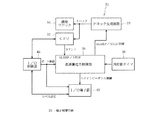
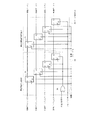
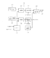
図25乃至図28は、本発明の第7実施例を示すものである。図25は、例えば車両用のボディECU(Electronic Control Unit) などに使用されるシングルチップマイクロコンピュータ(マイコン)の一構成例を示すものである。マイコン101は、CPU102を中心として、その周辺にメイン発振回路103,クロック制御回路104,CR発振回路105,ポート制御回路(信号レベル変化手段)106などを備えている。
(Seventh embodiment)
25 to 28 show a seventh embodiment of the present invention. FIG. 25 shows an example of the configuration of a single chip microcomputer (microcomputer) used in, for example, a vehicle body ECU (Electronic Control Unit). The microcomputer 101 includes a main oscillation circuit 103, a
メイン発振回路103は、マイコン101の外部に接続される水晶発振子107を発振させてCPU102に動作用のクロック信号(マシンクロック或いはシステムクロック)を供給するものである。クロック制御回路104は、CPU102によりアドレスバス108及びデータバス109を介してスリープ/ストップモードを開始させる指令が与えられると、メイン発振回路103に対してクロック停止信号を出力し、メイン発振回路103によるクロック信号の出力を停止させ、CPU102(若しくは、CPU102を含むマイコン101全体)をスリープ/ストップモードに設定する。
The main oscillation circuit 103 oscillates a
ここで、スリープモードとは、一旦移行するとクロック制御回路104に内蔵されているタイマで所定時間が経過した時点で自動的に解除されるモードを言うものとし、ストップモードとは、一旦移行すると外部においてウェイクアップ要因(後述するウェイクアップ信号など)が発生するまで解除されないモードを言うものとする。即ち、これらは、CPU102の動作状態を通常時よりも低下させることで消費電力の低下を図るモードである。
Here, the sleep mode refers to a mode in which a timer built in the
そして、クロック制御回路104は、ウェイクアップ要因の発生に応じてウェイクアップ信号WKUPが出力されると、クロック停止信号の出力を中止してメイン発振回路103によるクロック信号の出力を再開させるようになっている。尚、スリープモードにあっても、ウェイクアップ信号WKUPの出力によって当該モードは解除されるようになっている。
例えば、メイン発振回路103の発振周波数は4MHz程度であり、CR発振回路105の発振周波数は25kHz程度である。また、CPU102は、周波数4MHzのクロックを、内蔵するPLL発振回路(図示せず)で4逓倍して16MHzのクロック周波数で動作するようになっている。
When the wakeup signal WKUP is output in response to the occurrence of the wakeup factor, the
For example, the oscillation frequency of the main oscillation circuit 103 is about 4 MHz, and the oscillation frequency of the
ポート制御回路106は、CPU102が内部のレジスタに行う設定に応じて、マイコン101の出力端子(外部信号出力端子)110のレベル制御を行う回路である。また、ポート制御回路106には、クロック制御回路104によってスリープモード中に出力されるSLEEP信号が与えられている。
尚、具体的には図示しないが、マイコン101は、その他、割込みコントローラ,DMAコントローラ,ウォッチドッグタイマ,A/Dコンバータ,D/Aコンバータやシリアル通信回路などの周辺回路を備えている。
The
Although not specifically shown, the microcomputer 101 includes other peripheral circuits such as an interrupt controller, a DMA controller, a watchdog timer, an A / D converter, a D / A converter, and a serial communication circuit.
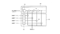
図26は、ポート制御回路106の内部構成を示す機能ブロック図である。タイマ(レベル変化用タイマ)111は、CR発振回路105によって出力されるCRクロック信号に基づいてカウント動作を行なうものであり、そのカウントデータは比較器(比較回路)112に与えられている。尚、タイマ111は、SLEEP信号がアクティブの場合カウント動作がイネーブルとなる。
FIG. 26 is a functional block diagram showing the internal configuration of the
比較器112には、出力タイミングレジスタ113の設定データも与えられており、比較器112は、両者のデータ値が一致すると、一致信号を一致保持部114を介してレベル設定部115に出力する。出力タイミングレジスタ113は、CPU102によるデータの書込みが可能に構成されたレジスタである。また、一致保持部114は、比較器112によって出力された一致信号のアクティブ状態を保持するフリップフロップである。
The setting data of the
レベル設定部115には、レベル選択部116において設定されたレベルの信号を、一致保持部114を介して与えられる一致信号をトリガとしてマイコン101の出力端子110に出力するものである。レベル選択部116は、出力タイミングレジスタ113と同様に、CPU102によるデータの書込みが可能に構成されたレジスタである。また、一致保持部114の出力状態は、CPU102が別途設けられているリセットレジスタに書込みを行なうことで、リセットする(S/Wリセット)ことが可能に構成されている。
The
尚、このポート制御回路106の機能は、以下のように動作させることを目的としたものである。即ち、CPU102がスリープモードからウェイクアップした場合に、マイコン101の端子に接続されている制御対象等の外部デバイスについて、何らかの処理を行なう必要があるとする。その時に、処理の前段階として、当該外部デバイスの機能をアクティブにする(例えば、動作用電源を投入する)ことが要求される場合に、CPU102がウェイクアップしてから全ての手順を踏むと、その処理が完了するまでに長い時間を要する。
そこで、第7実施例では、CPU102がスリープモードに移行している場合においても、その解除前の段階で出力端子110のレベルをハードウエア的に制御し、外部デバイスの機能を予めアクティブにすることを目的とする。
The function of the
Therefore, in the seventh embodiment, even when the
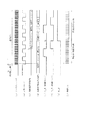
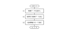
次に、第7実施例の作用について図27及び図28を参照して説明する。図27は、CPU102によるスリープモード移行処理の内容を示すフローチャートである。先ず、CPU102は、レベル選択部116に書込みを行なうことで、スリープモード中に変化させる出力端子110のレベルを設定する(例えば、L→H,ステップF1)。続いて、出力タイミングレジスタ113に書込みを行なうことで、スリープモード中のどのタイミングで出力端子110のレベルを変化させるかを設定する(ステップF2)。
Next, the operation of the seventh embodiment will be described with reference to FIGS. FIG. 27 is a flowchart showing the contents of the sleep mode transition process by the
それから、CPU102は、クロック制御回路104の図示しない内部レジスタに書込みを行なうことで、スリープモードの継続時間を設定すると(ステップF3)、クロック制御回路104に対してスリープコマンドを発行する(ステップF4)。すると、クロック制御回路104は、それを受けてメイン発振回路103に対してクロック停止信号を出力して発振動作を停止させる。並行して、クロック制御回路104は、ポート制御回路106に対してSLEEP信号を出力する。
Then, the
図28は、スリープモード移行中のタイミングチャートである。SLEEP信号がアクティブ(ハイ)になると(e)、メイン発振回路103によって出力されるマシンクロックは停止する(d)。そして、ポート制御回路106のタイマ111が、SLEEP信号の立ち上がりからカウント動作を開始する(b)。出力タイミングレジスタ113には、例えば設定データ「10」がセットされており(a)、タイマ111のカウント値が「10」に達すると、比較器112は一致信号を出力する。
FIG. 28 is a timing chart during the transition to the sleep mode. When the SLEEP signal becomes active (high) (e), the machine clock output by the main oscillation circuit 103 is stopped (d). Then, the
すると、その時点で、レベル設定部115は出力端子110の信号レベルをL(ロウ)からH(ハイ)に変化させる。ここで、出力端子110の信号レベルがハイに変化したことで、その出力端子110に接続されている外部デバイスはアクティブ状態となる。その後、設定されたスリープ継続期間が経過してCPU102がウェイクアップすると、CPU102は、当該外部デバイスに対して直ちに必要な処理を行うことが可能となる。そして、その処理を実行した後は、一致保持部114をS/Wリセットすることで、出力端子110の信号レベルを元に戻す。
At that time, the
以上のように第7実施例によれば、マイコン101のポート制御回路106は、CPU102がスリープモードに設定されている期間内に、出力端子110のレベルを変化させるようにした。従って、CPU102は、出力端子110のレベルを変化させるためだけに通常の動作モードを継続する必要がないので、消費電力を低減することができる。
そして、ポート制御回路106は、タイマ111のカウント値と出力タイミングレジスタ113のレジスタ値とを比較器112が比較し、両者が一致することでトリガ信号が出力されると出力端子110のレベルを変化させるので、レジスタ113に設定されるタイミングで、出力端子110のレベルを変化させることができる。また、そのレジスタ113は、CPU102によって任意のデータ値が設定可能に構成されるので、ユーザプログラムによってレベル変化タイミングを任意に設定することができる。
As described above, according to the seventh embodiment, the
Then, the
加えて、出力端子のレベル110は、スリープモードが解除されるとCPU102によってリセットすることが可能に構成されるので、CPU102が必要な処理を行った時点で出力端子のレベルを直ちにリセットすることができる。
In addition, since the
(第8実施例)
図29及び図30は、本発明の第8実施例を示すものであり、第7実施例と同一部分には同一符号を付して説明を省略し、以下異なる部分についてのみ説明する。第8実施例におけるポート制御回路117は、第7実施例の構成に機能を追加したものである。即ち、スリープ時間設定レジスタ118が追加されており、そのレジスタ118の設定データは、比較器119によってタイマ111のカウント値と比較される。
(Eighth embodiment)
29 and 30 show an eighth embodiment of the present invention. The same parts as those in the seventh embodiment are designated by the same reference numerals and the description thereof is omitted, and only different parts will be described below. The
比較器119は、両者が一致した時点で一致信号を割り込み発生部120に出力する。但し、割り込み発生部120は、比較器119によって一致信号が出力される以前に外部ウェイクアップ要因が発生し、スリープモードが解除された場合に、前記一致信号を受けてCPU102に割り込み要求を発生させるようになっている。即ち、タイマ111,スリープ時間設定レジスタ118,比較器119及び割り込み発生部120は、割り込み発生手段121を構成している。
The
次に、第8実施例の作用について図30をも参照して説明する。先ず、割り込み発生手段121の機能目的について述べる。スリープモードは、スリープ時間が経過する以前であっても外部要因の発生によって解除されるが、第7実施例の機能によってポート制御回路106が出力端子110のレベルを変化させた後に、外部要因の発生によって解除が行なわれると、次のような問題が発生する。
即ち、第7実施例において述べたように、ポート制御回路106が出力端子110のレベルを変化させる目的は、スリープモードが解除されると、CPU102が直ちに外部デバイスに対する処理を実行できるようにするためである。従って、出力端子110のレベルが変化した時点から、スリープモードがタイマによって解除されるまでの時間は、通常、外部デバイスをアクティブにするために必要最小限の時間に設定される。何故なら、この時間に冗長性を持たせると電流消費量が増加するからである。
Next, the operation of the eighth embodiment will be described with reference to FIG. First, the functional purpose of the interrupt generation means 121 will be described. The sleep mode is canceled by the occurrence of an external factor even before the sleep time elapses. However, after the
That is, as described in the seventh embodiment, the purpose of the
そのような事情において、スリープモードが、スリープ時間の経過前に解除されると、CPU102が起動した時点では、出力端子110のレベルを変化させてから必要な時間が経過していないため、外部デバイスが未だインアクティブ状態となっているおそれがある。そして、CPU102は、起動した時点では、本来の必要な時間が後どれ位なのかを知る手段がない。
Under such circumstances, if the sleep mode is canceled before the sleep time elapses, the required time has not elapsed since the level of the
そこで、第8実施例では、CPU102に対して本来必要であった時間を割り込みによって通知することを目的とする。即ち、図30に示すように、ポート制御回路117は、第7実施例と同様に出力端子110のレベルを変化させた後、外部要因の発生によって(f)スリープモードが早期解除されると(d,e)、割り込み発生部120がアクティブとなる。そして、本来のスリープ時間が経過して比較器119が一致信号を出力すると、その時点でCPU102に対して割り込みを発生させる。
従って、CPU102は、その割り込み信号によって、外部デバイスがアクティブとなったことが認識可能となり、必要な処理を行なった後に、出力端子110のレベルをS/Wリセットする。
Therefore, the eighth embodiment aims to notify the
Therefore, the
以上のように第8実施例によれば、割り込み発生手段121は、ポート制御回路117信号が出力端子110のレベルを変化させた後、解除要因の発生によってスリープモードが解除されると、図示しない解除タイマによってスリープモードが解除される予定のタイミングでCPU102に対して割り込み要求を発生させるようにした。したがって、CPU102は出力端子110について変化させた信号レベルの維持期間を把握できるようになり、その割り込み要求を認識した後、必要に応じて出力端子110のレベルをリセットすることができる。
As described above, according to the eighth embodiment, the interrupt generation means 121 is not shown when the sleep mode is canceled due to the generation of the cancellation factor after the
(第9実施例)
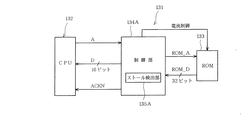
図31乃至図34は本発明の第9実施例を示すものである。マイクロコンピュータ131の構成を示す図31において、CPU132は、データバスが例えば16ビット構成であり、ROM133に記憶されているプログラムやデータを読み出して実行するようになっている。ROM133は、例えばフラッシュROMで構成されており、データバス幅はCPU132の2倍の32ビット構成となっている。
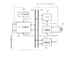
(Ninth embodiment)
31 to 34 show a ninth embodiment of the present invention. In FIG. 31 showing the configuration of the
そして、両者の間にはROMコントローラ(メモリインターフェイス回路装置)134が介在しており、CPU132は、ROMコントローラ134を介してROM133よりデータを読み出すようになっている。ROMコントローラ134は、CPU132によって出力された読出しアドレスAについて所定の操作を行なったアドレスROM_Aを出力してROM133よりデータROM_Dを読み出す。そのデータを適切なタイミングでCPU132側のデータバス上にデータDとして出力するようになっている。
即ち、マイコン101においては、フラッシュROMで構成されるROM133の読出し速度はCPU132の処理速度に比較して遅いため、ROM133側のデータバス幅をCPU132の2倍として、両者の間の調停制御をROMコントローラ134が行なうように構成されている。
A ROM controller (memory interface circuit device) 134 is interposed between the two, and the
That is, in the microcomputer 101, since the reading speed of the
図32は、ROMコントローラ134の内部構成を示すブロック図である。ROMコントローラ134は、制御部(データ読出し手段,読出し制御手段)135、アドレスパス部136、データパス部(読出し制御手段)137によって構成されている。制御部135は、アドレスパス制御部137、データパス制御部138、アドレスヒット検出部139、ROM制御部140及びCPU制御部141を備えている。
FIG. 32 is a block diagram showing an internal configuration of the
アドレスパス制御部137,データパス制御部138は、夫々アドレスパス部136,データパス部137の制御を行う。アドレスヒット検出部139は、アドレスパス部136が保持しているアドレスと、CPU132によって出力されたアドレスとの一致(ヒット)を検出するものである。CPU制御部141は、CPU132に対して読み出し制御信号(アクノリッジ信号ACKN)を出力する。尚、読み出し制御信号ACKNは、CPU132に対してROMデータ読出しをウエイトさせる場合にハイレベルとなり、ロウレベルではアクノリッジがアクティブであることを示している。そして、ROM制御部140は、これらを統括的に制御するようになっている。
The address path control
アドレスパス部136は、ROM133に対してマルチプレクサ(MUX)142を介してアドレスを出力するようになっている。そのMUX142の一方の入力側には、CPU132側のアドレスバスに直結されるスルーパス143が接続されており、他方の入力側にはカウンタ側パス144が接続されている。
スルーパス143には、バッファ(ラッチ)145の入力側も接続されており、バッファ(アドレス格納手段)145の出力側は、アドレスヒット検出部139に接続されている。バッファ145は、CPU132がデータ読み出しサイクルを実行した場合に出力されたアドレスが格納される。
The
The through
また、ビット出力部146は、ROM133のデータ読出し対象アドレスと、そのアドレスに応じたデータがバッファ145、及び後述するデータ用バッファ154に格納されている場合に、ROM読出しイネーブルを示すビット(バリッドビット)がセットされるように構成されており、その出力側もアドレスヒット検出部139に接続されている。尚、ビット出力部146のリセットは、ハードウエアによって行われる。
Further, the
一方、カウンタ側パス144側には、MUX147、カウンタバッファ(アドレス保持手段)148及びカウンタ(+4)149が配置されている。MUX147の一方の入力側にはスルーパス143が接続されており、他方の入力側には、カウンタ149の出力側が接続されている。そして、MUX147の出力端子は、カウンタバッファ148を介してカウンタ149の入力側及びカウンタ側パス144に接続されている。
また、カウンタ側パス144には、スルーパス143側と同様にバッファ150の入力側も接続されており、バッファ150の出力側は、アドレスヒット検出部139に接続されている。また、ビット出力部151の出力側もアドレスヒット検出部139に接続されている。
On the other hand, a
Similarly to the through
ビット出力部151は、ビット出力部146と同様に、ROM133の命令読出し対象アドレスと、そのアドレスに応じた命令がバッファ148、及び後述する命令用バッファ153に格納されている場合に、ROM読出しイネーブルを示すビットがセットされるように構成されている。そして、CPU132による命令読出しが連続したアドレスで行われている場合には、ROMコントローラ153,ROM133との間における1サイクル毎に、ビット出力部151及び153とCPU132側のアドレスAからヒット、ミスヒットを交互に検出することになる。
Similarly to the
データパス部137は、MUX152,命令用バッファ153、データ用バッファ154及びMUX155で構成されている。MUX152の入力側には、32ビットのROM_Dの内、上位16ビット[31:16],下位16ビット[15:0]が夫々接続されている。命令用バッファ153は、CPU132がROM133に対して命令読出し(インストラクションフェッチ)サイクルを実行した場合に、下位16ビットデータが格納される。
The
データ用バッファ154は、CPU132がROM133に対してデータ読出し(データロード)サイクルを実行した場合に、32ビットデータが格納される。そして、MUX155は、MUX152,命令用バッファ153、データ用バッファ154の上位側,下位側の何れかを選択してCPU132側のデータバスに出力するようになっている。
The
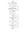
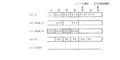
図33は、CPU132がROM133に対する読み出しサイクルを実行する場合におけるROMコントローラ134の制御内容を示すフローチャートである。また、図34は、CPU132が命令読出しサイクルを連続的に実行した場合のタイミングチャートである。尚、ROMコントローラ134は純粋にハードウエアのみで構成されており、図33のフローチャートは、そのハードウエアの動作を表したものである。
FIG. 33 is a flowchart showing the control contents of the
図34における動作概要を説明すると、CPU132は、命令読出しを16ビット(2バイト)単位で行う(a)。その場合、ROMコントローラ134は、自身がバッファ148に保持しているアドレスを、ROM133のデータバス幅32ビットに合わせて「4」ずつ増加させ、命令を32ビット(4バイト)単位で読み出すようになっている(b)。
そして、ROMコントローラ134は、同時に読み出した32ビットの命令の内、上位16ビットは読出しと同時にCPU132側のデータバスに出力し、下位16ビットは一旦バッファ153に格納する(h)。そして、CPU132が次の読み出しサイクルを実行した場合に、バッファ153に格納した命令を前記データバスに出力する(i)。
The operation outline in FIG. 34 will be described. The
The
また、制御部135は、CPUアドレスAと、カウンタバッファ148が保持しているアドレスとが一致すると、その次のサイクルにおいてアドレスを「4」増加させるためのカウントアップ信号を出力する(c)。同時に、カウンタバッファ148が保持しているアドレスをバッファ150に、また、ROM133より読み出されたデータをバッファ153にロードするためのロード信号を出力する(e)。
When the CPU address A matches the address held in the
図33において、制御部135は、外部の図示しないデコーダによるデコード信号の出力状態によってROM133に対する読み出しサイクルが発生するまで待機している(ステップG1)。そして、前記読み出しサイクルが発生すると(「YES」)、その読み出しサイクルが「命令読出し」であるか否かを判断する(ステップG2)。
In FIG. 33, the
A.<命令読出し:アドレス連続>
制御部135は、CPU132が出力する制御信号におけるアクセスコード等を参照し、「命令読出し」であると判断すると(ステップG2,「YES」)、次に、そのアドレスが命令用バッファ153にヒットしているか否かを判断する(ステップG3)。
前記アドレスに対応する命令が命令用バッファ153に格納されていればヒットであるから(「YES」)、制御部135は、カウンタ149によって「4」が加算されたアドレスにより(MUX147を介して)バッファ148の値を更新させる(ステップG4)。尚、制御部135は、ビット出力部151が「1」を出力している場合で、且つ、バッファ150に格納されているアドレスとCPU132側のアドレスAとが一致した場合に、命令の内下位16ビットがヒットしていると判断する。
A. <Instruction read: Address continuous>
When the
If the instruction corresponding to the address is stored in the
それから、MUX142を介してROM133側のアドレスバスに前記アドレスを出力させ、4バイト分の命令読出しを行う(ステップG5)。続いて、制御部135は、データパス部137の命令用バッファ153にヒットしている命令を、当該バッファ153よりCPU132側のデータバスに出力させる。
Then, the address is output to the address bus on the
ここで、図34を参照する。上記のケースは、例えば、サイクル(3)に対応する。即ち、CPU132がアドレス(A+2)を出力すると、そのアドレスに対応する命令D2は、ROMコントローラ134がその前のサイクル(1),(2)で行った読出しにおいて命令用バッファ153に格納されている。従って、この場合はバッファヒットとなり、命令D2はバッファ153より出力される。
それと同時に、バッファヒットとなった場合は、次回も命令が連続して(A+4)読み出される蓋然性が高いので、次回の命令読出しに備えてアドレス(A+4)による命令読出しを予め行なっておく。
Reference is now made to FIG. The above case corresponds to cycle (3), for example. That is, when the
At the same time, if there is a buffer hit, there is a high probability that instructions will be read continuously (A + 4) next time, so that instructions are read in advance using the address (A + 4) in preparation for the next instruction read.
再び、図33を参照する。ステップG3において、バッファヒットとならなかった場合(「NO」)、制御部135は、その時のアドレスが、現在読出しを行なっているアドレスに一致しているか否かを判断する(ステップG7)。そして、両者が一致している場合は(「YES」)、その時点で行われている読出しが完了するまでのセットアップ時間が経過するまで待機し(ステップG8,「YES」)、読み出されたデータの下位側16ビットでバッファ153の内容を更新する(ステップG9)。また、読み出されたデータの上位側16ビットは、そのままCPU132側のデータバスに出力する(ステップG10)。
FIG. 33 will be referred to again. If no buffer hit occurs in step G3 (“NO”), the
上記のケースは、例えば、図34のサイクル(4)に対応する。即ち、CPU132がアドレス(A+4)を出力すると、そのアドレスに対応する命令D4はバッファ153に格納されておらずバッファミスとなるが、アドレス(A+4)は、サイクル(3),(4)で行なっている読出しのアドレス(先読みアドレス)と一致している。従って、制御部135は、サイクル(4)で読み出されたデータの上位側D4をCPU132側のデータバスに出力し、下位側D6はバッファ153に格納する。
The above case corresponds to, for example, the cycle (4) in FIG. That is, when the
B.<命令読出し:分岐>
また、ステップG7において、その時のアドレスが先読みアドレスに一致しなかった場合は(「NO」)、プログラムにおいて分岐命令が実行された場合である。この時、制御部135は、先読みアドレス(カウンタバッファ148)を更新すると共に(ステップG11)、MUX142をスルーパス143側に切替えることでROMアドレスを更新する(ステップG12)。そして、ステップG8〜G10と同様の処理を行なう(ステップG13〜G15)。
B. <Instruction read: Branch>
In step G7, if the address at that time does not match the prefetch address (“NO”), this is a case where a branch instruction is executed in the program. At this time, the
C.<データ読出し>
ステップG2において、制御部135が「NO」と判断してステップG16に移行するケースは、CPU132がROM133に対してデータ読出しサイクルを行った場合である。CPU132がデータロードを行う場合、バイトアクセス,ワード(16ビット)アクセスの2つのケースがあるが、ROMコントローラ134は、何れであるかにかかわらず、読出し対象データが属する32ビット分のデータをROM133より同時に読み出すようになっている。また、その場合の読み出しアドレスは、バッファ145に格納される。
そして、その32ビットデータは常にデータ用バッファ154に格納されると共に、CPU132の読出し対象データが属する上位,下位16ビットの何れかは、MUX152,155を介してデータバスに出力される。
C. <Read data>
In step G2, the case where the
The 32-bit data is always stored in the
即ち、制御部135は、ステップG16において、読出しアドレスがデータ用バッファ154にヒットしたか否かを、バッファ145に格納されたアドレスとビット出力部146のビットに基づいて判断する。そして、ヒットした場合は(「YES」)データ用バッファ154よりヒットした側の16ビットデータをMUX155により選択してCPU132側のデータバスに出力する(ステップG17)。また、ステップG16において、読出しアドレスがデータ用バッファ154にヒットしなかった場合は(「NO」)、データについてステップG12〜G15と同様の処理を行なう(ステップG18〜G21)。
That is, in step G16, the
以上のように第9実施例によれば、ROMコントローラ134の制御部135は、バッファ148に保持されたアドレスに対して、CPU132が命令読み出しサイクルで出力したアドレスが一致すると、バッファ148に保持されたアドレス値を増加させてその次のサイクルでROM133よりデータを読み出す。そして、命令用バッファ153は、制御部135が読み出したデータをCPU132のバス幅を超えている分だけ格納し、制御部135は、CPU132が次回に連続するアドレスでROM133に対する命令読み出しサイクルを実行すると、命令用バッファ153が保持しているデータをCPU132のデータバスに出力するようにした。
As described above, according to the ninth embodiment, the
即ち、ROM133の読み出し速度が遅い場合でも、CPU132が連続するアドレス(CPU132のデータバス幅に応じた増分のアドレス)で命令読出しを行う場合は、次回以降に読み出そうとする命令は今回の読出しで同時に読み出されて命令用バッファ153に格納され、次回の読出しでは命令用バッファ153より命令が読み出される。従って、CPU132がROM133からの読み出しを行うために従来必要であったウエイトサイクルを削減することができ、処理効率を向上させることができる。
That is, even when the reading speed of the
また、CPU132がROM133に対するデータ読み出しサイクルを実行した場合は、読み出されたデータをデータ用バッファ154に格納し、制御部135は、CPU132が、次回にデータ読み出しサイクルを実行した場合にその読出しアドレスがデータ用バッファ154にヒットすれば、バッファ154に格納されているデータをCPU132のデータバスに出力する。即ち、データ用バッファ154は所謂データキャッシュとして作用することになるので、CPUは、データの読出し効率を向上させることが可能となる。
When the
<以下は参考>
Q.CPUと、このCPUよりも広いデータバス幅を構成する1つ以上のROMとの間に接続され、前記CPUが前記ROMよりデータを読み出そうとする場合に、その読み出しを制御するメモリインターフェイス回路装置であって、
アドレス値を保持する命令用アドレス保持手段と、
このアドレス保持手段に保持されたアドレスと、前記CPUが前記ROMに対する命令読み出しサイクルを実行するために出力したアドレスとを比較し、両者が一致した場合は、前記アドレス保持手段に保持されたアドレス値を、前記ROMのバス幅が前記CPUのバス幅を超えている分だけ増加させて、前記ROMよりデータを読み出すデータ読み出し手段と、
前記データ読み出し手段が読み出したデータを、前記ROMのバス幅が前記CPUのバス幅を超えている分だけ格納する命令用バッファと、
前記CPUが、次回に連続するアドレスで前記ROMに対する命令読み出しサイクルを実行すると、前記命令用バッファが保持しているデータを前記CPUのデータバスに出力させるように制御する読出し制御手段とを備えることを特徴とするメモリインターフェイス回路装置。
<The following is for reference>
Q. A memory interface circuit which is connected between the CPU and one or more ROMs having a data bus width wider than the CPU, and controls reading when the CPU attempts to read data from the ROM A device,
Instruction address holding means for holding an address value;
The address held in the address holding means is compared with the address output by the CPU to execute the instruction read cycle for the ROM, and if they match, the address value held in the address holding means Data read means for reading data from the ROM by increasing the ROM bus width exceeding the CPU bus width;
An instruction buffer for storing the data read by the data reading means for an amount that the ROM bus width exceeds the CPU bus width;
Read control means for controlling the data stored in the instruction buffer to be output to the data bus of the CPU when the CPU executes an instruction read cycle for the ROM at the next consecutive address. A memory interface circuit device.
上記Qのメモリインターフェイス回路装置によれば、データ読み出し手段は、アドレス保持手段に保持されたアドレスと、CPUが命令読み出しサイクルで出力したアドレスとが一致すると、アドレス保持手段に保持されたアドレス値を増加させてROMよりデータを読み出す。そして、命令用バッファは、データ読み出し手段が読み出したデータをCPUのバス幅を超えている分だけバッファリングし、読出し制御手段は、CPUが次回に連続するアドレスでROMに対する命令読み出しサイクルを実行すると、命令用バッファが保持しているデータをCPUのデータバスに出力する。 According to the memory interface circuit device of Q, the data reading means, when the address held in the address holding means matches the address output by the CPU in the instruction read cycle, the address value held in the address holding means is Read the data from the ROM in increments. Then, the instruction buffer buffers the data read by the data reading means as long as it exceeds the CPU bus width, and the read control means executes the instruction read cycle for the ROM at the next consecutive address. The data held in the instruction buffer is output to the CPU data bus.
即ち、ROMの読み出し速度が遅い場合でも、CPUが連続するアドレスで命令読出しを行う場合は、CPUが次回以降に読み出そうとする命令は今回の読出しで同時に読み出されて命令用バッファに保持され、次回の読出しでは命令用バッファより命令が読み出される。従って、CPUがROMからの読み出しを行うために従来必要であったウエイトサイクルを削減することができ、処理効率を向上させることができる。 In other words, even when the ROM read speed is slow, if the CPU reads instructions at consecutive addresses, the instructions that the CPU is to read from the next time are read simultaneously in the current read and held in the instruction buffer. In the next reading, the instruction is read from the instruction buffer. Therefore, it is possible to reduce the wait cycle conventionally required for the CPU to read from the ROM, and to improve the processing efficiency.
R.前記CPUが前記ROMに対するデータ読み出しサイクルを実行した場合に、前記データ読み出し手段が前記ROMより読み出したデータを、前記ROMのバス幅が前記CPUのバス幅を超えている分だけ格納するデータ用バッファと、
前記アドレスを格納するためのアドレス格納手段とを備え、
前記読出し制御手段は、前記アドレス格納手段に格納されているアドレスに基づいて、前記CPUが次回に前記ROMに対するデータ読み出しサイクルを実行した場合に、その読み出しアドレスに対応するデータが前記データ用バッファに格納されていると判断すると、前記データを前記CPUのデータバスに出力させるように制御することを特徴とする上記Qのメモリインターフェイス回路装置。
R. When the CPU executes a data read cycle for the ROM, a data buffer for storing the data read from the ROM by the data read means as much as the bus width of the ROM exceeds the bus width of the CPU When,
Address storage means for storing the address,
When the CPU next executes the data read cycle for the ROM based on the address stored in the address storage means, the read control means stores data corresponding to the read address in the data buffer. The memory interface circuit device according to Q, wherein if it is determined that the data is stored, the data is controlled to be output to a data bus of the CPU.
上記Rのメモリインターフェイス回路装置によれば、CPUがデータ読み出しサイクルを実行した場合にROMより読み出されたデータを、ROMのバス幅がCPUのバス幅を超えている分だけデータ用バッファに格納する。また、この時、前記読出しアドレスはアドレス格納手段に格納される。そして、読出し制御手段は、CPUが次回にデータ読み出しサイクルを実行した場合に、その読み出しアドレスに対応するデータがデータ用バッファに格納されていると判断すると、そのデータをCPUのデータバスに出力させる。
即ち、データ用バッファは所謂データキャッシュとして作用するので、データの読出しアドレスがデータ用バッファにヒットした場合、CPUはそのデータを高速に読み出すことができる。従って、データの読出し効率を向上させることが可能となる。
According to the above R memory interface circuit device, when the CPU executes a data read cycle, the data read from the ROM is stored in the data buffer by the amount that the ROM bus width exceeds the CPU bus width. To do. At this time, the read address is stored in the address storage means. When the CPU executes the data read cycle next time and determines that the data corresponding to the read address is stored in the data buffer, the read control means outputs the data to the CPU data bus. .
That is, since the data buffer functions as a so-called data cache, when the data read address hits the data buffer, the CPU can read the data at high speed. Therefore, it is possible to improve the data reading efficiency.
(第10実施例)
図35及び図36は本発明の第10実施例を示すものであり、第9実施例と異なる部分についてのみ説明する。図35に示すように、第10実施例では、ROMコントローラ134Aの制御部135Aは、CPU132がストール状態となったことを検出する機能を有しており、その場合に、ROM133の電流を遮断する制御を行うように構成されている。
(Tenth embodiment)
FIGS. 35 and 36 show a tenth embodiment of the present invention, and only the parts different from the ninth embodiment will be described. As shown in FIG. 35, in the tenth embodiment, the control unit 135A of the
図36に示すタイミングチャートにおいて、制御部135Aは、CPU132の動作にストールが発生したことを、例えばアドレス値(A+4)が2サイクル続けて同じ値であることによってサイクル(5)のタイミングで検出する。
その後、CPU132のストール状態が例えば更に2サイクル継続すると、制御部135Aは、ROM133の消費電流をカットするように制御する。尚、ここで言う「ストール」とは、一般的な意味におけるCPU132内部の演算処理の停止に加えて、ROM133に対するアクセスが行われない状態(例えば、RAMやI/O等の他のリソースに対してアクセスを行っている場合)も含むものとする。その場合は、外部のデコーダのデコード信号によってROM133がセレクトされなくなることで判定できる。例えば、図33のステップG1において、「NO」と判断している期間を計測して判定することが可能である。
In the timing chart shown in FIG. 36, the control unit 135A detects that the stall has occurred in the operation of the
After that, when the stall state of the
以上のように第10実施例によれば、ROMコントローラ134Aの制御部135Aは、CPU132がストール状態となったことを検出するとROM133からのデータ読み出しを停止させる。そして、CPU132のストール状態が所定期間継続すると、ROM133における消費電流を遮断するようにした。従って、無駄な電力消費を低減することができる。
As described above, according to the tenth embodiment, the control unit 135A of the
<以下は参考>
S.前記読出し制御手段は、前記CPUの動作にストールが発生したことを検出可能に構成され、
前記データ読み出し手段は、前記ストールが発生したことが検出された場合に、前記ROMに対するデータの読み出しが実行中である場合は、その読み出し処理を継続して完了させることを特徴とする上記Q,R,下記Uの何れかのメモリインターフェイス回路装置。
上記Sのメモリインターフェイス回路装置によれば、データ読み出し手段は、CPUの動作にストールが発生したことが検出された場合でも、ROMに対するデータの読み出しが実行中である場合は、その読み出し処理を継続して完了させる。即ち、ストールが発生した時点で直ちに読出しを中止することがないので、読出し効率を向上させることができる。
<The following is for reference>
S. The read control means is configured to be able to detect that a stall has occurred in the operation of the CPU,
The data reading means, when it is detected that the stall has occurred, and when the reading of data to the ROM is being executed, the reading process is continued and completed, Q, R, the memory interface circuit device of any one of U below.
According to the memory interface circuit device of S, the data reading means continues the reading process when data reading from the ROM is being executed even when it is detected that the CPU operation has stalled. To complete. That is, since reading is not immediately stopped when a stall occurs, reading efficiency can be improved.
T.前記読出し制御手段は、前記CPUの動作にストールが発生したことを検出し、そのストール状態が所定期間継続すると、前記ROMにおける消費電流を遮断するように制御することを特徴とする上記Q,R,下記Uの何れかのメモリインターフェイス回路装置。
上記Tのメモリインターフェイス回路装置によれば、読出し制御手段は、CPUのストール状態が所定期間継続すると、ROMにおける消費電流を遮断するように制御するので、無駄な電力消費を低減することができる。
T.A. The read control unit detects that a stall has occurred in the operation of the CPU, and controls the current consumption in the ROM to be cut off when the stall state continues for a predetermined period. The memory interface circuit device of any one of U below.
According to the memory interface circuit device of T, the read control means controls to cut off the current consumption in the ROM when the stall state of the CPU continues for a predetermined period, so that it is possible to reduce wasteful power consumption.
本発明は上記し且つ図面に記載した実施例にのみ限定されるものではなく、以下のような変形または拡張が可能である。
第1実施例において1/N分周器19,20は必要に応じて設ければ良い。
第2実施例において、メインクロック監視部7は削除しても良い。
また、第2実施例においてステップA0,A4は削除して実施しても良い。
また、第2実施例において、高速補正動作は、必ずしもバイナリサーチ方式で行なうものに限らず、比較的大なる調整信号データから開始して、その絶対値が次第に小さくなるようにして行えば良い。
第5実施例において、発振回路装置の発振動作を停止させる場合は、低消費電力モードの実行に伴うものに限ることはない。即ち、発振回路装置が出力するクロック信号は、CPUの動作用クロック信号として供給されるものに限らず、どのような用途であっても良い。従って、その用途に応じてクロック信号の出力を一時的に停止させた後、出力を再開させる必要があるものであれば、広く適用が可能である。
The present invention is not limited to the embodiments described above and shown in the drawings, and the following modifications or expansions are possible.
In the first embodiment, the 1 /
In the second embodiment, the main
In the second embodiment, steps A0 and A4 may be deleted.
In the second embodiment, the high-speed correction operation is not necessarily performed by the binary search method, but may be performed by starting from relatively large adjustment signal data and gradually decreasing the absolute value thereof.
In the fifth embodiment, the oscillation operation of the oscillation circuit device is not limited to the one accompanying the execution of the low power consumption mode. That is, the clock signal output from the oscillation circuit device is not limited to the one supplied as the operation clock signal for the CPU, and may be used for any purpose. Therefore, the present invention can be widely applied as long as it is necessary to temporarily stop the output of the clock signal according to the use and then restart the output.
第7実施例において、出力タイミングレジスタ113に設定されるデータは、ハードウエア的に固定されているように構成しても良い。
第8実施例において、レベル変化用タイマを解除タイマと共通にすれば、より簡単に構成することができる。
また、第8実施例において、割り込み発生用のタイマを、レベル変化用タイマと独立に備えても良い。
また、マイコン101に、CPU102の動作を監視するためのウォッチドッグタイマ、若しくは、CPU102の動作用クロックとは独立にカウント動作するフリーランタイマなどを備えている場合、レベル変化用タイマを、それら他のタイマと共通とすることで、構成をより簡単にすることができる。但し、この場合、レベル変化用タイマとして使用する場合は、そのタイマ動作の開始時点におけるウォッチドッグタイマ等のカウント値を読み出し、出力タイミングに相当するカウント値を加算したものを出力タイミングレジスタに設定する。そして、タイマを共通にすることで、ソフトウエアの作成管理が容易となり、バグが発生する可能性を低下させることができる。
In the seventh embodiment, the data set in the
In the eighth embodiment, if the level change timer is shared with the release timer, the configuration can be simplified.
In the eighth embodiment, an interrupt generation timer may be provided independently of the level change timer.
If the microcomputer 101 is provided with a watchdog timer for monitoring the operation of the
第9実施例において、メモリインターフェイス回路装置が内蔵するバッファのバス幅を、ROMのデータバス幅よりも広くするように構成しても良い。斯様に構成すれば、データ読み出し手段がROMに対する読出しを複数回行なって、前記バッファにデータを格納することでより多くのデータについてその先読みを行なうことができる。
第9または第10実施例において、ROMを、16ビットバス構成のマットを2個並べて同様に実施しても良い。また、その場合、ROMコントローラ134による読出し対象となっていないマットのROMについては消費電流を遮断するように構成しても良い。斯様に構成しても、ROMが複数マットで構成されている場合に、無駄な電力消費を低減することができる。
In the ninth embodiment, the bus width of the buffer built in the memory interface circuit device may be made wider than the data bus width of the ROM. If comprised in this way, the data read-out means will perform the read-out with respect to ROM several times, and it can pre-read about more data by storing data in the said buffer.
In the ninth or tenth embodiment, the ROM may be similarly implemented by arranging two 16-bit bus mats. In this case, the current consumption of the mat ROM that is not read by the
更に、第10実施例において、CPU132がスリープ/ストップなどの低消費電力モードに移行した場合は、ROMの全ての消費電流を遮断するように構成しても良い。斯様に構成すれば、無駄な電力消費を低減することができる。
また、第10実施例において、ROMコントローラ134Aを、CPU132のストール検出タイミングが例えばサイクル(4)でアドレス(A+2)が継続した場合に、その時点でROM133に対して実行中である命令のデータD2,D4の読出しがその他の条件により続行可能であれば、続行して完了させるようにする。斯様に構成すれば、ROMコントローラ134Aは、ストール状態を検出しても直ちにROM133に対する読出しを停止することがないので、読出し効率を向上させることができる。
Further, in the tenth embodiment, when the
In the tenth embodiment, if the
<以下は参考>
U.前記バッファのバス幅は、前記ROMのデータバス幅よりも広く構成されていることを特徴とする請求項30または31記載のメモリインターフェイス回路装置。
上記Uのメモリインターフェイス回路装置によれば、バッファのバス幅を、ROMのデータバス幅よりも広くするので、データ読み出し手段が読出しを複数回行なって、前記バッファにデータを格納すれば、より多くのデータについてその先読みを行なうことができる。
<The following is for reference>
U. 32. The memory interface circuit device according to claim 30, wherein the buffer has a bus width wider than a data bus width of the ROM.
According to the memory interface circuit device of U, the bus width of the buffer is made wider than the data bus width of the ROM. Therefore, if the data reading means performs reading a plurality of times and stores data in the buffer, more data is stored. This data can be prefetched.
V.前記ROMが、複数マットで構成されている場合、
前記読出し制御手段は、前記データ読み出し手段による読出し対象となっているROM以外の消費電流を遮断するように制御することを特徴とする請求項34記載のメモリインターフェイス回路装置。
上記Vのメモリインターフェイス回路装置によれば、読出し制御手段は、データ読み出し手段による読出し対象となっているROM以外の消費電流を遮断するので、ROMが複数マットで構成されている場合に、無駄な電力消費を低減することができる。
V. When the ROM is composed of a plurality of mats,
35. The memory interface circuit device according to
According to the memory interface circuit device of the above V, the read control means cuts off the current consumption other than the ROM that is read by the data read means, so that it is useless when the ROM is composed of a plurality of mats. Power consumption can be reduced.
W.前記読出し制御手段は、前記CPUが、内部状態を保持したまま動作を一時的に停止する低消費電力モードに移行した場合は、前記ROMの全ての消費電流を遮断するように制御することを特徴とする上記S又はTのメモリインターフェイス回路装置。
上記Wのメモリインターフェイス回路装置によれば、読出し制御手段は、CPUが低消費電力モードに移行した場合は、ROMの全ての消費電流を遮断するので、無駄な電力消費を低減することができる。
W. The read control means controls the CPU to cut off all current consumption of the ROM when the CPU shifts to a low power consumption mode in which the operation is temporarily stopped while maintaining the internal state. The S or T memory interface circuit device.
According to the memory interface circuit device of W, the read control means cuts off all the current consumption of the ROM when the CPU shifts to the low power consumption mode, so that it is possible to reduce wasteful power consumption.
1はマイクロコンピュータ、2はCPU、3はメインクロック発振部(発振回路)、4はサブクロック発振部(CR発振回路)、5はウォッチドッグタイマ、6はサブクロック補正部(補正回路)、7はメインクロック監視部(監視回路)、8はエッジ検出回路8、9はパルスカウンタ、10カウント数設定レジスタ、11は比較調整手段、13はラダー抵抗(可変抵抗器)、21はクロック制御回路装置、31はマイクロコンピュータ、32はCPU、35は低消費電力制御部(端子制御手段)、42は入出力端子(外部信号端子)、51はマイクロコンピュータ、52はCPU、54は外部発振子、55はDPLL回路(周波数逓倍回路)、56はクロック制御部(切替通知制御部)、62はステートカウンタ(シーケンス制御手段)、71はECU(マイクロコンピュータ)、71aはクロック制御回路(発振回路装置)、76は発振回路、77は周波数逓倍回路、78は低消費電力制御回路(低消費電力制御手段)、80は制御回路(シーケンス制御手段)、81はDCO、83はリングオシレータ(多相クロック信号出力手段)、95は周波数情報保持回路部(データ保持手段)、101はシングルチップマイクロコンピュータ、102はCPU、106はポート制御回路(信号レベル変化手段)、110は出力端子(外部信号出力端子)、111はタイマ(レベル変化用タイマ)、112は比較器(比較回路)、113は出力タイミングレジスタ、117はポート制御回路、121は割り込み発生手段、131はマイクロコンピュータ、132はCPU、133はROM、134,134AはROMコントローラ(メモリインターフェイス回路装置)、135,135Aは制御部(データ読出し手段,読出し制御手段)、137はデータパス部(読出し制御手段)、145はバッファ(アドレス格納手段)、148はカウンタバッファ(アドレス保持手段)、153は命令用バッファ、154はデータ用バッファを示す。 1 is a microcomputer, 2 is a CPU, 3 is a main clock oscillation unit (oscillation circuit), 4 is a subclock oscillation unit (CR oscillation circuit), 5 is a watchdog timer, 6 is a subclock correction unit (correction circuit), 7 Is a main clock monitoring unit (monitoring circuit), 8 is an edge detection circuit 8, 9 is a pulse counter, 10 count number setting register, 11 is a comparison adjustment means, 13 is a ladder resistor (variable resistor), 21 is a clock control circuit device , 31 is a microcomputer, 32 is a CPU, 35 is a low power consumption control unit (terminal control means), 42 is an input / output terminal (external signal terminal), 51 is a microcomputer, 52 is a CPU, 54 is an external oscillator, 55 Is a DPLL circuit (frequency multiplication circuit), 56 is a clock control unit (switch notification control unit), 62 is a state counter (sequence control means), 1 is an ECU (microcomputer), 71a is a clock control circuit (oscillation circuit device), 76 is an oscillation circuit, 77 is a frequency multiplication circuit, 78 is a low power consumption control circuit (low power consumption control means), and 80 is a control circuit ( Sequence control means), 81 a DCO, 83 a ring oscillator (multi-phase clock signal output means), 95 a frequency information holding circuit (data holding means), 101 a single chip microcomputer, 102 a CPU, 106 a port control Circuit (signal level changing means), 110 is an output terminal (external signal output terminal), 111 is a timer (level change timer), 112 is a comparator (comparison circuit), 113 is an output timing register, 117 is a port control circuit, 121 is an interrupt generating means, 131 is a microcomputer, 132 is a CPU, 133 is RO , 134 and 134A are ROM controllers (memory interface circuit devices), 135 and 135A are control sections (data reading means, reading control means), 137 is a data path section (reading control means), 145 is a buffer (address storage means), Reference numeral 148 denotes a counter buffer (address holding means), 153 denotes an instruction buffer, and 154 denotes a data buffer.
Claims (6)
前記低消費電力モードを周期的に解除するための解除タイマと、
前記低消費電力モードが設定されている期間内に、外部信号出力端子のレベルを変化させる信号レベル変化手段とを備えて構成され、
前記信号レベル変化手段は、
前記外部信号出力端子のレベルを変化させるタイミングを設定するためのレジスタと、
前記CPUが低消費電力モードに移行した時点からカウント動作を開始するレベル変化用タイマと、
前記レベル変化用タイマのカウント値と前記レジスタの値とを比較して、両者が一致するとトリガ信号を出力する比較回路とを備え、前記トリガ信号が出力されると、前記外部信号出力端子のレベルを変化させるように構成されていることを特徴とするマイクロコンピュータ。 A CPU configured to be able to set a low power consumption mode in which the operation is temporarily stopped while maintaining the internal state;
A release timer for periodically releasing the low power consumption mode;
A signal level changing means for changing the level of the external signal output terminal within a period in which the low power consumption mode is set ;
The signal level changing means is
A register for setting a timing for changing the level of the external signal output terminal;
A level change timer that starts a count operation from the time when the CPU enters the low power consumption mode;
Comparing the count value of the level change timer with the value of the register, and a comparator circuit that outputs a trigger signal when both match, and when the trigger signal is output, the level of the external signal output terminal A microcomputer characterized by being configured to change .
前記信号レベル変化手段が前記外部信号出力端子のレベルを変化させた後、前記解除要因の発生によって低消費電力モードが解除されると、前記解除タイマによって前記低消費電力モードが解除される予定のタイミングで、前記CPUに対して割り込み要求を発生させる割り込み発生手段を備えたことを特徴とする請求項3記載のマイクロコンピュータ。 The low power consumption mode is set so as to be released even when a release factor other than the release timer occurs,
After the signal level changing means changes the level of the external signal output terminal, when the low power consumption mode is canceled due to the generation of the release factor, the low power consumption mode is scheduled to be released by the release timer. 4. The microcomputer according to claim 3 , further comprising interrupt generation means for generating an interrupt request to the CPU at timing.
The release timer claim 1, characterized in that it is constituted by a common free-run timer count operation independently of the operation clock of the watchdog timer, or the CPU to monitor the operation of the CPU 5. The microcomputer according to any one of 4 to 4 .
Priority Applications (1)
| Application Number | Priority Date | Filing Date | Title |
|---|---|---|---|
| JP2007322364A JP4780098B2 (en) | 2007-12-13 | 2007-12-13 | Microcomputer |
Applications Claiming Priority (1)
| Application Number | Priority Date | Filing Date | Title |
|---|---|---|---|
| JP2007322364A JP4780098B2 (en) | 2007-12-13 | 2007-12-13 | Microcomputer |
Related Parent Applications (1)
| Application Number | Title | Priority Date | Filing Date |
|---|---|---|---|
| JP2002380002A Division JP4082211B2 (en) | 2002-12-27 | 2002-12-27 | Microcomputer |
Related Child Applications (1)
| Application Number | Title | Priority Date | Filing Date |
|---|---|---|---|
| JP2011091371A Division JP5293767B2 (en) | 2011-04-15 | 2011-04-15 | Microcomputer |
Publications (2)
| Publication Number | Publication Date |
|---|---|
| JP2008123538A JP2008123538A (en) | 2008-05-29 |
| JP4780098B2 true JP4780098B2 (en) | 2011-09-28 |
Family
ID=39508151
Family Applications (1)
| Application Number | Title | Priority Date | Filing Date |
|---|---|---|---|
| JP2007322364A Expired - Fee Related JP4780098B2 (en) | 2007-12-13 | 2007-12-13 | Microcomputer |
Country Status (1)
| Country | Link |
|---|---|
| JP (1) | JP4780098B2 (en) |
Families Citing this family (3)
| Publication number | Priority date | Publication date | Assignee | Title |
|---|---|---|---|---|
| JP5365108B2 (en) | 2008-09-04 | 2013-12-11 | ミツミ電機株式会社 | Semiconductor integrated circuit |
| JP2010066809A (en) * | 2008-09-08 | 2010-03-25 | Sanyo Electric Co Ltd | Microcomputer |
| US9430026B2 (en) | 2011-11-09 | 2016-08-30 | Toyota Jidosha Kabushiki Kaisha | Electronic control device and microcomputer control method |
Family Cites Families (7)
| Publication number | Priority date | Publication date | Assignee | Title |
|---|---|---|---|---|
| JPH01137355A (en) * | 1987-11-25 | 1989-05-30 | Hitachi Ltd | Output circuit for one-chip microprocessor |
| JPH0573349A (en) * | 1990-10-17 | 1993-03-26 | Nec Corp | Stand-by control circuit |
| JPH096750A (en) * | 1995-06-16 | 1997-01-10 | Hitachi Ltd | Terminal state control circuit and microcomputer |
| JPH0934867A (en) * | 1995-07-24 | 1997-02-07 | Mitsubishi Electric Corp | Microcomputer |
| JP3082721B2 (en) * | 1997-09-19 | 2000-08-28 | 日本電気株式会社 | Timer device |
| JP3711849B2 (en) * | 2000-08-21 | 2005-11-02 | 株式会社デンソー | Microcomputer |
| JP3829916B2 (en) * | 2000-12-28 | 2006-10-04 | 株式会社デンソー | Microcomputer |
-
2007
- 2007-12-13 JP JP2007322364A patent/JP4780098B2/en not_active Expired - Fee Related
Also Published As
| Publication number | Publication date |
|---|---|
| JP2008123538A (en) | 2008-05-29 |
Similar Documents
| Publication | Publication Date | Title |
|---|---|---|
| JP4082211B2 (en) | Microcomputer | |
| JP4535170B2 (en) | Microcomputer system | |
| TWI527051B (en) | Training, power-gating, and dynamic frequency changing of a memory controller | |
| JP3817743B2 (en) | Semiconductor integrated circuit device, semiconductor device and electronic apparatus including the same | |
| US7681057B2 (en) | Power management of non-volatile memory systems | |
| JPH10149226A (en) | Power management method and device for multifunctional controller equipped with microprocessor | |
| US20110214003A1 (en) | Clock control signal generation circuit, clock selector, and data processing device | |
| JP3437174B2 (en) | Power saving integrated circuit and control method of power saving integrated circuit | |
| JP4780098B2 (en) | Microcomputer | |
| US7296170B1 (en) | Clock controller with clock source fail-safe logic | |
| JP3988636B2 (en) | Microcomputer and vehicle ECU | |
| JP2002328839A (en) | Data processing device and data processor | |
| US6381705B1 (en) | Method and device for reducing current consumption of a microcontroller | |
| JP4715839B2 (en) | Memory interface circuit device | |
| JP4715760B2 (en) | Microcomputer and control system | |
| JP5293767B2 (en) | Microcomputer | |
| JP2006127466A (en) | Microcomputer | |
| JPH0844594A (en) | Data processor | |
| JP4152795B2 (en) | Microcontroller | |
| JP5324340B2 (en) | Microcomputer | |
| JP4659627B2 (en) | Electronics | |
| JP7316902B2 (en) | Information processing device, its control method, and program | |
| JP2005071203A (en) | Microprocessor | |
| JPH1049248A (en) | Microcomputer | |
| US6973353B1 (en) | Programmable controller for controlling an output state |
Legal Events
| Date | Code | Title | Description |
|---|---|---|---|
| A131 | Notification of reasons for refusal |
Free format text: JAPANESE INTERMEDIATE CODE: A131 Effective date: 20100928 |
|
| A521 | Written amendment |
Free format text: JAPANESE INTERMEDIATE CODE: A523 Effective date: 20101122 |
|
| A02 | Decision of refusal |
Free format text: JAPANESE INTERMEDIATE CODE: A02 Effective date: 20110215 |
|
| A521 | Written amendment |
Free format text: JAPANESE INTERMEDIATE CODE: A523 Effective date: 20110415 |
|
| A911 | Transfer of reconsideration by examiner before appeal (zenchi) |
Free format text: JAPANESE INTERMEDIATE CODE: A911 Effective date: 20110425 |
|
| TRDD | Decision of grant or rejection written | ||
| A01 | Written decision to grant a patent or to grant a registration (utility model) |
Free format text: JAPANESE INTERMEDIATE CODE: A01 Effective date: 20110607 |
|
| A01 | Written decision to grant a patent or to grant a registration (utility model) |
Free format text: JAPANESE INTERMEDIATE CODE: A01 |
|
| A61 | First payment of annual fees (during grant procedure) |
Free format text: JAPANESE INTERMEDIATE CODE: A61 Effective date: 20110620 |
|
| FPAY | Renewal fee payment (event date is renewal date of database) |
Free format text: PAYMENT UNTIL: 20140715 Year of fee payment: 3 |
|
| FPAY | Renewal fee payment (event date is renewal date of database) |
Free format text: PAYMENT UNTIL: 20140715 Year of fee payment: 3 |
|
| R250 | Receipt of annual fees |
Free format text: JAPANESE INTERMEDIATE CODE: R250 |
|
| R250 | Receipt of annual fees |
Free format text: JAPANESE INTERMEDIATE CODE: R250 |
|
| R250 | Receipt of annual fees |
Free format text: JAPANESE INTERMEDIATE CODE: R250 |
|
| R250 | Receipt of annual fees |
Free format text: JAPANESE INTERMEDIATE CODE: R250 |
|
| LAPS | Cancellation because of no payment of annual fees |