JP4737913B2 - Liquid crystal display element and method for driving liquid crystal display element - Google Patents
Liquid crystal display element and method for driving liquid crystal display element Download PDFInfo
- Publication number
- JP4737913B2 JP4737913B2 JP2002123998A JP2002123998A JP4737913B2 JP 4737913 B2 JP4737913 B2 JP 4737913B2 JP 2002123998 A JP2002123998 A JP 2002123998A JP 2002123998 A JP2002123998 A JP 2002123998A JP 4737913 B2 JP4737913 B2 JP 4737913B2
- Authority
- JP
- Japan
- Prior art keywords
- liquid crystal
- crystal display
- alignment
- transition
- region
- Prior art date
- Legal status (The legal status is an assumption and is not a legal conclusion. Google has not performed a legal analysis and makes no representation as to the accuracy of the status listed.)
- Expired - Fee Related
Links
Images


Abstract
Description
【0001】
【発明の属する技術分野】
本発明は、高速応答で広視野角の表示性能を持つ液晶表示素子、液晶表示素子用基板、液晶表示装置、液晶表示素子の製造方法、及び液晶表示素子の駆動方法に関し、特に、光学補償ベンドモードセル(Optically self-Compensated Birefringence mode cell)タイプのスプレイ−ベンド転移の容易なものに関する。
【0002】
【従来の技術】
マルチメディア技術の進展とともに、ますます画像情報の占める割合が多くなってきている。最近では液晶技術の発展により、高コントラストで広視野角の液晶ディスプレイが開発及び実用化され、CRTディスプレイと比肩するレベルにまでなってきた。
【0003】
しかしながら、現行の液晶ディスプレイでは、応答速度が遅いことから動画表示において残像のため画像がぼやけるという問題を有しており、この点においてCRTディスプレイに劣っている。
【0004】
液晶ディスプレイにおける高速応答化の試みは過去から数多くなされてきている。高速応答の種々の液晶表示方式については、Wuらによりまとめられている(C.S. Wu and S.T. Wu, SPIE, 1665, 250 (1992))が、動画像表示に必要な応答特性が期待出来る方式及び方法は限られている。
【0005】
すなわち、現行のNTSCシステムにおいては1フレーム(16.7msec)以内で液晶が追随する必要があるが、現行の液晶ディスプレイでは白黒二値間では充分速い応答性を示すものの、多階調表示を行った場合の階調間応答では100msec以上の遅い応答となってしまう。特に駆動電圧の低い領域での階調間応答は著しく遅い。
【0006】
現在、動画表示に適した高速応答性を有する液晶ディスプレイとしては、OCBモード液晶表示素子、あるいは強誘電性液晶表示素子、反強誘電性液晶表示素子がその可能性を有している。
【0007】
しかしながら、層構造を有する強誘電性液晶表示素子、及び反強誘電性液晶表示素子は耐衝撃性が弱い、使用温度範囲が狭い、特性の温度依存性が大きいなど実用的な意味での課題が多く、現実的にはネマティック液晶を用いるOCBモード液晶表示素子が動画像表示に適した液晶表示素子として有望視されている。
【0008】
このOCBモード液晶表示素子は、1983年にJ.P.Bosによりその高速性が示された表示方式であり、その後、フィルム位相差板と組み合わせることにより広視野角及び高速応答性が両立するディスプレイであることが示され研究開発が活発化した。
【0009】
このモ−ドの液晶表示素子は、図14に示すように、透明電極2が形成されているガラス基板1と、透明電極7が形成されているガラス基板8と、基板1、8間に配置される液晶層4とを有する。電極2、7上には配向膜3、6が形成され、この配向膜3、6には、液晶分子を平行かつ同一方向に配向させるべく配向処理がなされている。また、基板1、8の外側には、偏光板13、16がクロスニコルに配設されており、この偏光板13、16と基板1、8との間には位相補償板17、18が介在している。
【0010】
このような構造の液晶セルは、電圧印加によりセル中央部にベンド配向あるいはツイスト配向を含んだベンド配向を誘起させることと、低電圧駆動と視野角拡大のために位相補償板17、18を配設することを特徴とするものであり、性能的には中間調表示域においても高速応答が可能であると同時に広い視野角特性を有している。
【0011】
なお、OCBモード液晶表示素子は、通常、液晶パネル内部の液晶がベンド配向を維持するような電圧で動作させるが、ある電圧以下になると、ベンド配向状態よりもスプレイ配向状態の方が安定になるため、スプレイ配向への転移が発生する。この転移は不可逆であり、一旦スプレイ配向が発生した画素は、その後、液晶表示素子上で表示欠陥(輝点)として残り、その正常表示動作を妨げる。
【0012】
【発明が解決しようとする課題】
ところで、OCBモードでは、初期のスプレイ配向状態4aから電圧印加によりベンド配向状態4bに転移させる初期化処理が必要不可欠である。
【0013】
しかしながら、数V程度の電圧印加では初期化処理に分単位の時間が必要であり、OCBモードの課題の一つになっている。そのため、数V程度の電圧印加により容易にベンド配向が形成される、転移速度の速い液晶表示素子が望まれている。
【0014】
一方、OCB型液晶表示モードのスプレイ配向からベンド配向への転移(以下、スプレイ−ベンド転移という)を高速化するための技術が特開平11-7018号公報に開示されている。その技術として、液晶にカイラル剤を添加した例、液晶パネル全面で均一に180度ツイストを形成した例、液晶パネル全面で均一に10度ツイストを形成した例が示されている。しかし、これらの技術は、スプレイ−ベンド転移を高速化するには十分ではない。そして、このスプレイ−ベンド転移が確実に行われず、局所的にスプレイ配向の領域が残存すると、そこが輝点となって点欠陥のように見えるという問題があった。
【0015】
本発明はこのような課題を解決するためになされたもので、スプレイ配向からベンド配向への転移が速くかつ確実な液晶表示素子及び液晶表示素子の駆動方法を提供することを目的としている。
【0016】
【課題を解決するための手段】
上記課題を解決するために、本件発明者は、上記スプレイ−ベンド転移の挙動を観察した。すると、ある特定の個所からベンド配向の核が発生し、これが成長していくことを見出した。さらに、本件発明者は、鋭意検討した結果、局所的にツイスト配向を形成することで、これを核としてベンド転移が発生することを見出した。
【0018】
また、本発明に係る液晶表示素子は、一対の基板とこれら基板間に配置された液晶層とを有するOCBモードの液晶表示素子であり、前記一対の基板にはともに略平行な配向処理がなされており、前記配向処理による液晶分子の配向方位とは異なる方位のツイスト配向を局所的に形成することで異配向方位領域を形成する手段を有したものである。
【0214】
また、本発明に係る液晶表示素子の駆動方法は、上記液晶表示素子の駆動方法であって、一方の前記基板上にソース線、ゲート線、及び画素電極が形成されるとともに他方の前記基板に対向電極が形成され、前記異配向方位領域を形成する期間に、前記ゲート線に特定符号のゲート電圧を印加し、前記ソース線に前記ゲート電圧と逆符号の電圧を、前記対向電極には前記ゲート電圧と同符号の電圧を印加する期間が存在するようにしたものである。
【0216】
また、本発明に係る液晶表示素子の駆動方法は上記液晶表示素子の駆動方法であって、一方の前記基板上にソース線、ゲート線、及び画素電極が形成されるとともに他方の前記基板に対向電極が形成され、前記異配向方位領域を形成する期間に、相隣合う前記ソース線に交互に異なる電圧を印加するようにしたものである。
【0255】
【発明の実施の形態】
以下、本発明の実施の形態について図面を参照しながら説明する。
実施の形態1
本発明の実施の形態1は、配向方位が他の領域の配向方位と異なる領域(以下、異配向方位領域という)又はツイスト配向領域を有するパラレル配向型液晶表示素子を例示したものである。
[テストセル]
以下の実施例1〜3においては、テストセルとしての液晶表示素子を作製し、その作製したテストセルについて、スプレイ−ベンド転移時間を評価した。スプレイ−ベンド転移時間の評価には位相補償板は不要であるので、実施例1〜3のテストセルでは位相補償板を省略している。
(実施例1)
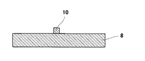
図1は本実施の形態の実施例1に係るテストセルの構成を模式的に示す断面図、図15は図1のテストセルの下側基板の突起の配置を模式的に示す平面図である。図5は図1の基板のラビング方向を示す図である。
【0256】
図1、図15に示すように、本実施例に係るテストセルAは、一対の基板、すなわち上側基板101及び下側基板102がビーズ状のスペーサ5を介して対向配置され、上側基板101及び下側基板102の間に形成された空間にネマティック液晶からなる液晶層4が配置されている。
【0257】
上側基板101は、ガラス基板1の下面に透明電極2及び配向膜3が順に積層形成されて構成されている。また、下側基板102は、ガラス基板8の上面に三角柱形状の突起10が形成され、その突起10が形成されたガラス基板8の上面を覆うように、透明電極7及び配向膜6が順に積層形成されて構成されている。従って、下側基板102の上面には突起(立体障害)103が形成されている。
【0258】
図5に示すように、突起103はその横断面形状の三角形の頂点がラビング方向を向くように形成されている。これにより、実施の形態2で詳述するように突起103の周囲にツイスト配向領域が形成されている。
【0259】
なお、図1ではスペーサ5を2個のみ示しているが、実際には多数のスペーサ5が両基板101,102間に不規則な間隔で介在している。
【0260】
次に、このように構成されたテストセルの製造方法を図2〜図4を用いて説明する。図2及び図3は図1のテストセルの製造プロセスを示す断面図、図4はフォトマスクを示す平面図である。
【0261】
まず、図2(a)に示すように、ガラス基板8上に、JSR株式会社製PC系レジスト材料を塗布して、厚さ0.5μmのフォトレジスト薄膜20を形成する。次いで、そのフォトレジスト薄膜20に、図4に示す三角形状のパターン開口部22を有するフォトマスク21を通して平行光紫外線23を照射し、該フォトレジスト薄膜20を露光する。次いで、その露光されたフォトレジスト薄膜20を現像してリンスし、その後90℃でプリベークする。これにより、図3に示すように、ガラス基板8上に、フォトレジスト薄膜からなる、三角形の横断面形状を有する(図15参照)柱状の突起10が形成される。
【0262】
次いで、その突起10が形成されたガラス基板8上に、定法に従い、ITO(indium tin oxide)を2000オングストロームの厚みに成膜し、それにより透明電極7を形成する。次いで、その透明電極7が形成されたガラス基板8上に、日産化学工業製配向膜塗料SE−7492をスピンコート法にて塗布し、これを恒温槽中にて180℃で1時間加熱して硬化させ、それにより配向膜6を形成する。これにより、上面に突起103を有する下側基板102が完成する。
【0263】
また、上記突起10が形成されたガラス基板8と同様に、ガラス基板1上に透明電極2及び配向膜3を形成する。これにより上側基板101が完成する。
【0264】
次いで、上側基板101及び下側基板102に、レーヨン製ラビング布を用いて、図5に示す方向にラビング処理を施す。
【0265】
次いで、上側基板101と下側基板102とを、積水ファインケミカル(株)製スペーサ5及びストラクトボンド352A(三井東圧化学(株)製シール樹脂の商品名)を用いて、基板間隔が6.5μmとなるように貼り合わせ、それにより液晶セル9を作製する。ここで、上記ラビング処理は、この液晶セル9の配向膜界面における液晶プレチルト角が約5度となるように行われる。
【0266】
次いで、その液晶セル9に、液晶MJ96435(屈折率異方性Δn=0.138)を真空注入法にて注入して封止する。これによりテストセルAが完成する。
【0267】
次に、以上の製造方法により作製されたテストセルAのスプレイ−ベンド転移時間の評価を説明する。
【0268】
まず、テストセルAの上面及び下面に、各々の偏光軸が配向膜のラビング処理方向と45度の角度をなし、かつ、互いの偏光軸方向が直交するように2枚の偏光板を貼り付け、その後、透明電極2,7間に7Vの矩形波電圧を印加してスプレイ配向からベンド配向への転移を観察したところ、約5秒で電極2,7の全領域がスプレイ配向からベンド領域へと転移した。
【0269】
つまり、テストセルAは、突起103付近の領域では、液晶の配向方位が周囲の領域の液晶の配向方位とは異なっており、この領域においては液晶層4は若干のツイスト配向をしている。そして、電圧印加により、この領域は速やかにスプレイ−ベンド転移が進行し、この領域からベンド配向が周囲の領域に広がっていく。すなわち、確実かつ高速なスプレイ−ベンド転移が達成出来る。
【0270】
比較例として、突起103を有しない点を除いて同じ構成を有するテストセルRを、テストセルAと同様のプロセスで作製し、そのスプレイ−ベンド転移時間を測定した。この測定では、テストセルRに7Vの矩形波電圧を印加した時の、電極の全領域がスプレイ配向からベンド領域へと転移するに要する時間は42秒であった。従って、本発明の効果は明らかである。
【0271】
なお、本実施例においては、突起103を片方の基板102にのみ形成したが、両方の基板に形成してもよいことは言うまでもない。また、本実施例では突起103として、横断面形状が三角形のものを用いたが、ラビング処理により、液晶の配向方位が部分的に周囲の領域とは異なった領域が形成されれば他の形状を有する突起であってもよい。具体的には、その横断面形状が円形、楕円形、菱形、あるいは三角形である柱状体、山形状体、又は錐状体が好ましい。
(実施例2)
図6は本実施の形態の実施例2に係るテストセルの構成を模式的に示す断面図、図16は図6のテストセルの下側基板の溝の配置を模式的に示す平面図である。
【0272】
図6、図16に示すように、本実施例に係るテストセルBは、実施例1とは異なり、下側基板102に溝104が形成されている。すなわち、下側基板102は、ガラス基板8の上面に溝30が形成され、その溝30が形成されたガラス基板8の上面を覆うように、透明電極7及び配向膜6が順に積層形成され、それによりその上面に溝104が形成されるようにして、構成されている。溝104は、ラビング方向(全体的な配向処理の方向)に対して30度傾斜するように形成され、かつラビング方向に直角な方向に500オングストロームのピッチで複数本(本実施例では20本)列設されている。溝104は、液晶配向効果を有する溝(マイクログルーブ)となるような幅を有するように形成されている。つまり、溝104の幅は、液晶層4の液晶分子が該溝104にはまり込んでその方向に配向されるような幅、本実施例では約100オングストロームの幅に形成されている。これにより、液晶層4の、溝104が列設された領域にツイスト配向領域が形成されている。これ以外の点は、実施例1と同様である。なお、図6では溝30及び溝104を誇張して描いている。
【0273】
次に、以上のように構成されたテストセルBの製造方法を図6、図7、図16を用いて説明する。図7はフォトマスクを示す平面図である。
【0274】
まず、ガラス基板8上に、実施例1と同様にして厚さ0.5μmのフォトレジスト薄膜20を形成し、そのフォトレジスト薄膜20にフォトマスク21を用いて溝30を形成する。フォトマスク21には、図7に示すように、スリット状の開口部22が、基準方向に対して30度傾斜するように形成され、かつ基準方向に直角な方向に500オングストロームのピッチで20本列設されている。開口部22の幅は、以降の工程を経て最終的に配向膜6上に形成される溝104が約100オングストロームの幅を有するような幅に設定されている。また、基準方向は、フォトマスク21を用いて下側基板102上に形成される溝104がラビングされるべき方向である。
【0275】
以降、上面に溝30が形成されたガラス基板8上に、実施例1と同様にして、透明電極7及び配向膜6が形成され、上面に溝104が形成された下側基板102が完成される。上側基板101は実施例1と全く同様に作製される。
【0276】
そして、以上のように作製した上側基板101及び下側基板102を実施例1と同様にラビング処理する。下側基板102のラビング方向は図16に示す方向である。この際、溝104は、深さが幅に比して深い(0.5μm)ためラビングされない。つまり、溝104は、上述のように、液晶層4の液晶分子がはまり込んで配向されるような狭い幅を有し、かつラビング処理時にラビングされないような深さを有することが要求される。上側基板101のラビング方向は、液晶セルに組立てた状態で下側基板102のラビング方向に平行となる方向である。
【0277】
その後、実施例1と同様にして、液晶セル9を作製し、その液晶セル9に液晶を封入してテストセルBを完成する。配向膜界面での液晶プレチルト角は、実施例1と同様、約5度である。
【0278】
次に、以上の製造方法により作製されたテストセルBのスプレイ−ベンド転移時間の評価を説明する。
【0279】
まず、テストセルBの上面及び下面に、各々の偏光軸が配向膜のラビング処理方向と45度の角度をなし、かつ、互いの偏光軸方向が直交するように2枚の偏光板を貼り付け、その後、透明電極2,7間に7Vの矩形波電圧を印加してスプレイ配向からベンド配向への転移を観察したところ、約7秒で電極2,7の全領域がスプレイ配向からベンド配向へと転移した。
【0280】
これは、テストセルBは、溝104が列設された領域では、液晶の配向方位が周囲の領域の液晶の配向方位とは異なっており、この領域においては液晶層4はツイスト配向をしている。そのため、実施例1と同様に、電圧印加によって、そのツイスト配向領域において速やかにスプレイ−ベンド転移が進行し、その転移により生じたベンド配向が周囲の領域に広がっていくことにより、確実かつ高速なスプレイ−ベンド転移が達成されるものである。本実施例は、表示画素領域内に液晶配向効果を有する溝104を部分的に設け、それによってツイスト配向領域を部分的に形成することにより、確実かつ速やかなスプレイ−ベンド転移を促すものであり、その実用的価値は極めて大きい。
【0281】
なお、本実施例では、溝30,104をフォトリソグラフィー法により形成したが、これをスタンプ法(例えば、E.S. Lee et. al., "Control of Liquid Crystal Alignment Using Stamped-Morphology Method" , Jpn. J. Appl. Phys., Part 2, vol.32, pp.L1436-L1438, 1993.)等の他の方法により形成してもよいことは言うまでもない。
【0282】
また、本実施例では、溝104のラビング方向に対する傾斜角度を30度としたが、この傾斜角度は90度以下であればよく、60度以上90度以下とするのが好ましい。この理由については、実施の形態2で詳述する。また、複数の溝104は、ラビング方向に対する角度がそれぞれ異なっていてもよく、また、列状に限らず任意の態様に配置してもよく、さらに、不規則に配置してもよい。
(実施例3)
図8は本実施の形態の実施例3に係るテストセルの構成を模式的に示す断面図、図17は図8のテストセルの下側基板の配向処理状態を模式的に示す平面図である。
【0283】
図8、図17に示すように、本実施例に係るテストセルCは、実施例1とは異なり、上側基板101及び下側基板102が光配向により配向処理されている。すなわち、上側基板101及び下側基板102は、それぞれ、ガラス基板1,8上に透明電極2,7及び配向膜3,6が順に積層形成されて構成されている。下側基板102は、図17に示すように、その上面に碁盤の目状に多数の単位配向処理領域(異方向配向処理領域)51が形成され、その多数形成された単位配向処理領域51が、相隣り合うもの同士51A,51Bが90度異なる配向方位を有するように配向処理されている。また、上側基板101は、下側基板102の各単位配向処理領域に対応する各単位配向処理領域が、その対応する下側基板101の各単位配向処理領域と同じ配向方位を有するようにそれぞれ配向処理されている。従って、各単位配向処理領域51上の液晶層4はパラレル配向をしており、ツイスト配向をしてはいない。なお、各単位配向処理領域における液晶4の中央部分の液晶分子の配向方位は多少のバラツキ(分布)を有していてもよい。また、配向膜3,6は光感応性を有する配向膜で構成され、光配向によって配向処理されている。これ以外の点は、実施例1と同様である。
【0284】
次に、以上のように構成されたテストセルCの製造方法を図8、図9、図10を用いて説明する。図9は図8のテストセルの製造プロセスを示す断面図、図10はマスクを示す平面図である。
【0285】
まず、実施例1と同様に、ガラス基板8上に透明電極7を形成する。次いで、この透明電極7が形成されたガラス基板8上にポリビニルシンナメートの2wt.%溶液(モノクロロベンゼンとジクロロメタンの1:1混合溶液中に希釈)をスピンコート法にて塗布し、これを恒温槽中にて100℃で1時間乾燥し、それにより光感応性を有する配向膜6を形成する。これにより、下側基板102が作製される。また、これと全く同様にして、上側基板101を作製する。
【0286】
次いで、下側基板102の配向膜6に偏光紫外線照射装置(図示せず)を用いて以下のように光配向処理を施す。以下の配向処理では、波長365nmの偏光紫外線が1mW/cm2の照射光強度で照射される。すなわち、まず、下側基板102の配向膜6に、マスク21を介して、図9に符号32で示す方向(紙面に平行な方向)に延在する偏波面を有する偏光紫外線を30分間照射する(処理A)。この時の偏光紫外線の照射角度θは90度である。また、マスク21は、図17に示す碁盤の目状の単位配向処理領域51において1つ置きに位置する単位配向処理領域51Aに対応する形状及び位置を有するように、開口部122が形成されている。
【0287】
次いで、マスク21を下側基板102の単位配向処理領域1つ分だけずらし、さらに偏波面を90度回転させて、すなわち偏波面が図9の紙面に垂直な方向に延在するようにして、偏光紫外線を30分間照射する(処理B)。この時の偏光紫外線の照射角度θは90度である。
【0288】
次いで、偏光紫外線の照射角度θを45度、照射時間を3分間に変えて、上記処理A及び処理Bを行う(処理A’、処理B’)。これにより、下側基板102の光配向処理が完了する。
【0289】
次いで、上側基板101に、下側基板102と同様に、上記処理A、処理B、処理A’、処理B’を施し、それにより上側基板101の光配向処理を完了する。
【0290】
次いで、実施例1と同様にして、液晶セル9を作製し、その液晶セル9に液晶を封入してテストセルCを完成する。この時、配向膜界面での液晶プレチルト角は、本実施例では、上側基板101及び下側基板102に対する上記処理A’及び処理B’の結果として約3度となった。
【0291】
次に、以上の製造方法により作製されたテストセルCのスプレイ−ベンド転移時間の評価を説明する。
【0292】
まず、テストセルCの上面及び下面に、各々の偏光軸が、互いに配向方位が90度異なる2種類の単位配向領域の液晶分子の平均配向方位と45度の角度をなし、かつ、互いの偏光軸方向が直交するように2枚の偏光板を貼り付け、その後、透明電極2,7間に7Vの矩形波電圧を印加してスプレイ配向からベンド配向への転移を観察したところ、約4秒で電極2,7の全領域がスプレイ配向からベンド配向へと転移した。
【0293】
これは、液晶層4の各単位配向処理領域51上の領域、すなわち異配向方位領域から転移核が発生し、それが成長してスプレイ−ベンド転移が進行するため、高速な転移が可能であり、かつ異配向方位領域が多数形成されているため、確実な転移が可能なものである。
【0294】
なお、本実施例では、単位配向処理領域を特に画素と対応させていないが、これを画素と対応させてもよい。
[液晶表示素子]
(実施例4)
図11は本実施の形態の実施例4に係る液晶表示素子の構成を示す断面図、図12は図11の液晶表示素子の各光学素子の配置方向を示す平面図である。なお、図11では下側基板102の突起103(図1参照)の記載を省略している。図11に示すように、本実施例に係る液晶表示素子Dは、実施例1に係るテストセルAの上面に、主軸がハイブリット配列した負の屈折率異方性もつ光学媒体よりなる位相差板(位相補償板)12、負の一軸性位相差板(位相補償板)11、正の一軸性位相差板(位相補償板)19、偏光板13が順に配設され、該テストセルAの下面に、主軸がハイブリット配列した負の屈折率異方性もつ光学媒体よりなる位相差板(位相補償板)15、負の一軸性位相差板(位相補償板)14、偏光板16が順に配設されている。これら位相差板12,15,11,14,19、及び偏光板16は、テストセルAのラビング方向に対して図12に示す方向となるように配置されている。
【0295】
位相差板12,15,11,14,19のリターデーション値は、本実施例では、波長550nmの光に対して、それぞれ、26nm、26nm、350nm、350nm、及び150nmである。
【0296】
次に、以上のように構成された液晶表示素子Dの性能の評価を説明する。
【0297】
図13は、25℃における液晶表示素子Dの正面における電圧−透過率特性を示すグラフである。この電圧−透過率特性は、液晶表示素子Dに10Vの矩形波電圧を10秒印加してベンド配向に転移していることを確認した後、電圧を降下させながら透過率を測定することにより求めた。液晶表示素子Dではベンド配向からスプレイ配向への転移が2.1Vで起こるため、実効的には2.2V以上の電圧で表示を行う必要がある。一方、この電圧−透過率特性では7.2V近傍で透過率が極小となっている。そこで、白レベル電圧を2.2V、黒レベル電圧を7.2Vとし、この時のコントラスト比の視角依存性を測定した。その結果、上下126度、左右160度の範囲でコントラスト比10:1以上が達成されており、基板配向膜面上に液晶ダイレクタの方向が周囲とは異なる部位を部分的に設けても、充分な広視野角特性が維持されることが確認された。また、目視観察においても、配向不良及び表示品位不良は認められなかった。
【0298】
また、印加電圧を3Vから5Vへ変化させた場合の応答時間を測定したところ、立ち上がり時間は5ミリ秒であり、印加電圧を5Vから3Vへ変化させた場合の応答時間を測定したところ、立ち下がり時間は6ミリ秒であった。
(実施例5)
本実施の形態の実施例5に係る液晶表示素子(図示せず)は、実施例4の液晶表示素子DにおいてテストセルAに代えて実施例2に係るテストセルBを用いたものである(図示せず)。このような構成としても、実施例4と同様の効果が得られる。
(実施例6)
本実施の形態の実施例6に係る液晶表示素子(図示せず)は、実施例4の液晶表示素子DにおいてテストセルAに代えて実施例3に係るテストセルCを用いたものである(図示せず)。但し、光学素子は図18に示す方向に配置される。
【0299】
このような構成としても、実施例4と同様の効果が得られる。
【0300】
以上より明らかなように、実施の形態1に係る液晶表示素子においては、従来のOCBモードの広視野角特性や応答特性を犠牲にすることなく、高速なスプレイ−ベンド配向転移を達成することが出来、その実用的な価値は極めて大きい。
実施の形態2
本発明の実施の形態2は、ラビングによる配向処理制御用の突起(立体障害)の好ましい形態を例示したものである。
【0301】
図19は本発明の実施の形態2に係る液晶表示素子の構成を示す平面図、図20は図19のXX−XX矢視断面図である。
【0302】
図19、図20に示すように、本実施の形態の液晶表示素子Eは、アクティブマトリクスタイプのOCBモードの液晶表示素子であり、TFT基板(アレイ基板)202と該TFT基板202に対向するように配置されたカラーフィルタ基板201との間に形成された空間にネマッティック液晶からなる液晶層4が配置されて構成されている。なお、図19、図20では位相差板、偏光板等の光学素子の記載を省略している。
【0303】
TFT基板202はガラス基板8を有している。ガラス基板8の上面には、画素電極64が形成され、それを覆うように絶縁層68が形成されている。絶縁層68上にはゲート線61及びソース線62がマトリクス状に形成され、それらを覆うように絶縁層91が形成されている。ゲート線61及びソース線62は、それらで区画された画素63の領域内に画素電極64が位置するように形成されている。絶縁層91上には、ゲート線61の上方に位置するように補助容量電極65が形成され、該補助容量電極65が形成された絶縁層91の表面を覆うように絶縁層77が形成されている。そして、補助容量電極65の上方には、フォトレジストからなる複合柱スペーサ203’が形成されている。複合柱スペーサ203’は補助容量電極65毎、すなわち、画素63毎に形成され、3本の柱スペーサ203A’,203B’,203C’(図19には203C’のみを示す)で構成されている。また、複合柱スペーサ203’は、絶縁層77が部分的に除去されて補助容量電極65上に直接形成されたものと、補助容量電極65上に絶縁層77を介して形成されたものとがソース線62の延在方向において2対1の比率で配置されている。そして、これら、複合柱スペーサ203、絶縁層77、補助容量電極65の表面を覆うように配向膜6が形成されている。符号203は表面に配向膜6が形成された複合柱スペーサ203’を、符号203A,203B,203Cは、表面に配向膜6が形成された各柱スペーサ203A’,203B’,203C’を表している。補助容量電極65上に絶縁層77を介して形成された複合柱スペーサ203の先端はカラーフィルタ基板201の下面に当接し、補助容量電極65上に直接形成された複合柱スペーサ203の先端は、カラーフィルタ基板201の下面との間に、絶縁層77の厚みに相当する隙間を有している。なお、図19、図20では複合柱スペーサ203を誇張して描いている。また複合柱スペーサ203については、後でさらに詳述する。また、符号66はTFT(Thin Film Transistor)を示す。
【0304】
カラーフィルタ基板201は、ガラス基板1の下面にブラックマトリクス67、カラーフィルタ76、対向電極79、配向膜3が順に積層形成されて構成されている。ブラックマトリクス67は、ゲート線61及びソース線62の上方に位置するように配置されている。カラーフィルタ基板201及び複合柱スペーサ203を含むTFT基板202は、周知のフォトリソグラフィー法により製造されるので、その説明を省略する。また、カラーフィルタ基板201及びTFT基板202から液晶表示素子への組立は実施の形態1の実施例1と同様である。
【0305】
次に、複合柱スペーサ203について図19〜図22を用いて詳しく説明する。図21は複合柱スペーサ203の形態を示す平面図、図22は図21の複合柱スペーサによって形成された配向処理状態を示す概念図である。
【0306】
液晶表示素子Eは、2枚の基板201,201間に液晶4を封入している。ここで2枚の基板210,202には配向処理をラビングによって施したが、このラビング方向69は上側基板(カラーフィルタ基板)201及び下側基板(TFT基板)202とも同じ方向とした。本発明は、片側の基板(本実施の形態では下側基板201)上にフォトレジストによって柱スペーサ(立体障害)を形成し、その柱スペーサの形態を特定のものにすることを特徴とする。一般に従来の液晶表示素子では、基板間に分散させた樹脂ビーズを基板間隔を保つスペーサとしていた。本発明ではこの樹脂ビーズの代わりにこのフォトレジストからなる柱スペーサをスペーサとして兼用している。なお、本実施の形態では、柱スペーサ203A,203B,203Cは電極(ここでは補助容量電極65)上に形成されているが、逆に柱スペーサ203A,203B,203Cの表面を電極が覆っていてもよい。但し、柱スペーサ203A,203B,203Cの表面を電極が覆っている場合には、相手方の基板(ここではカラーフィルタ基板201)の電極(ここでは対向電極79)の、該柱スペーサ203A,203B,203Cの先端に対応する部分を除去しておく必要がある。さもないと、両電極間でショートする可能性があるからである。
【0307】
本発明の柱スペーサの形態の一例として、本実施の形態では、図21に示すように、各辺がラビング方向69に対して傾斜した菱形断面形状を有する柱状の柱スペーサ203A,203B,203Cを3個形成し、これを1組(以下、複合柱スペーサ203という)として、各画素63に規則的に形成した。ここで、本明細書において、複合柱スペーサとは、互いに近接して配置された複数の柱スペーサからなる柱スペーサ群をいう。
【0308】
複合柱スペーサ203は、その3個の柱スペーサ203A,203B,203Cが、いずれも、その菱形断面形状の短い方の対角線がラビング方向69に平行となるような向きに形成されている。ここで、柱スペーサ203A,203B,203Cの断面形状(平面形状)は異方性を有しているのが好ましい。また、本実施の形態の骨子がラビングの流れを制御することにあるので、上記断面形状はラビングが流れやすいことが重要である。そこで、これらの観点から、本実施の形態では、柱スペーサ203A,203B,203Cの断面形状として菱形を採用した。また、ラビング方向69とは、基板に対するラビング布の相対的移動方向、つまり、全体的な配向処理の方向をいう。3個の柱スペーサ203A,203B,203Cは、2個の柱スペーサ203A,203Bがラビング方向69に対して横方向に所定の間隔で並ぶように配置され、残りの1個の柱スペーサ203Cが前記2個の柱スペーサ203A,203Bの後方に位置しかつ該2個の柱スペーサ203A,203Bに対し同じ間隔を有するよう配置されている。そして、後側に位置する柱スペーサ(以下、後側柱スペーサという)203Cは、前側に位置する2個の柱スペーサ(以下、前側柱スペーサという)203A,203Bより大きい断面積を有している。
【0309】
この複合柱スペーサ203が形成された基板202をラビングすると、この複合柱スペーサ203の形態に従って配向処理方向、すなわち実際にラビングされた方向が局所的に制御される。この配向処理状態を図22に示す。
【0310】
図22において、符号69を付した矢印はラビング方向を示す。また、実線の矢印は実際のラビングの流れ、すなわち配向処理方向を示し、幅広の矢印81は局所的な配向処理方向を示している。特に重要なのは後側柱スペーサ203Cであり、これに当たったラビング布の繊維(図示せず)は左右にはじかれ、それによって、矢印81a,81bで示すように、左右の方向にラビングがなされる。そして、このように左右の方向になされたラビングの上にさらに通常方向(ラビング方向69)のラビングがなされることを防ぐために前側柱スペーサ203A,203Bが形成されている。これにより、図22に示すように、複合柱スペーサ203の周辺部に、周囲の領域71の配向処理方向(全体的な配向処理方向)と異なる方向に配向処理された局所的な異方向配向処理領域70が形成される。一方、上側基板201には上記周囲の領域71と同じ方向に配向処理が施されている。従って、この下側基板202の異方向配向処理領域70の上方に位置する液晶層4はツイスト配向状態になる。そして、この液晶層4のツイスト配向状態になった領域(以下、ツイスト配向領域という)が核となってスプレイ−ベンド転移が進行する。このツイスト配向領域の中でも、特にスプレイ−ベンドベンド転移の核になる箇所は、図22に×印で示した個所であり、ツイストが発生する領域であった。
【0311】
次に、複合柱スペーサ203の形態についての好ましい条件を説明する。前側柱スペーサ203A,203Bと後側柱スペーサ203Cとの距離が離れすぎると柱スペーサ203A,203BA,Bの有する遮蔽効果が少なくなる。この遮蔽効果を有効に発揮させるためには、柱スペーサ203C付近に発生する異方向ラビング領域を通常方向にラビングされないように遮蔽する必要がある。そこで、複合柱スペーサ203の高さと遮蔽距離との関係を求めたところ、本実施の形態の複合柱スペーサ203では、複合柱スペーサ203からの距離が複合柱スペーサ203の高さの5倍以下となる領域で遮蔽効果が見られた。3倍以下の領域では確実な遮蔽効果が得られた。一方、5倍以上離れると遮蔽効果はなくなった。また、複合柱スペーサ203の高さを半分にすると遮蔽距離も半分になったので、遮蔽距離は確かに複合柱スペーサ203の高さの関数である。
【0312】
また、前側に位置する2個の柱スペーサ203A,203B同士の間隔は、ラビング布の繊維径よりも広いことが必要である。本実施の形態では、10μm以上とするのが好ましい。また前側柱スペーサ203A,203Bと後側柱スペーサ203Cとの間の領域には、前側柱スペーサ203A,203Bによるラビングの影が発生し、この影領域では実際にラビングされる方向が周囲の領域71とは異なっている。また、この影領域ではプレチルト角も変化していることが確認された。この影が柱スペーサ203Cに届くことが転移を効率的に行うために必要であった。本実施の形態では、この影が届く距離は複合柱スペーサ203の高さの5倍以下でかつ約25μm以下であった。従って、前側柱スペーサ203A,203Bと後側柱スペーサ203Cとを離しすぎると転移が効率的に行われない。また、本実施の形態のように、前側柱スペーサ203A,203Bの断面積よりも後側柱スペーサ203Cの断面積が大きいと、この影による効果が大きい。これは、前側柱スペーサ203A,203Bの影が後側柱スペーサ203Cによって形成されたラビング(配向処理)と接触する可能性が大きくなるためである。
【0313】
また、各柱スペーサ203A,203B,203Cの菱形断面の短い方の対角線の長さが5μm以上であることが好ましい。この対角線の長さが短いと、柱スペーサが倒れやすいからである。なお、柱スペーサが任意の形状の断面を有する場合にはその最小径が5μm以上であるのが好ましい。ここで、本明細書において、柱スペーサ(立体障害)の径とは、柱スペーサの断面の中心点を挟む該断面外周上の2点間の距離をいう。
【0314】
また、スプレイ−ベンド転移の核を生じさせるためには、液晶層4にツイスト配向が発生していることが最低限必要とされる。そして、互いに異なる方向の配向状態が接している個所で転移が発生しやすく、特に本実施の形態ではツイスト方向が異なるツイスト配向領域が接している個所が核になりやすかった。この箇所は、上述したように、図22において×印で示した箇所(正確には×印で示した箇所上の液晶)であり、この箇所では右回りツイストの領域と左回りツイストの領域とが接している。従って、柱スペーサは、このような互いに異なる方向の配向状態が接する個所が生じるような形態とするのが望ましく、さらに、互いにツイスト方向が反対である領域が接する箇所が形成されるようなものとするのがより望ましい。
【0315】
また、本実施の形態の柱スペーサ203A,203B,203Cや実施の形態1の実施例1の突起103(図1参照)を含む、基板上に形成された突起の付近が、転移の核となりやすかった。これは、ラビング時に、突起の後側ではラビングの影が生じ、その影によってラビング強度が弱い部分が形成される一方、プレチルト角はラビングの強度に依存する。そのため、突起の前側ではラビング強度が強くてプレチルト角が低く、後側ではラビング強度が弱くてプレチルト角が比較的高くなる。その結果、突起の手前と後とではプレチルト角が異なることとなり、デフェクトが発生しやすくなる。そして、このデフェクトが発生しているとそれが核になりやすいからであると考えられる。このデフェクトは、転移電圧を印加した際に、セルの厚み方向の中央部において、液晶分子が上方向又は下方向に向いたスプレイ状態と他の状態との境界をなすデフェクトである。
【0316】
また、この突起は、液晶層4の厚み(本明細書においてはセル厚と呼ぶ)の半分以上の高さを有すると転移核になりやすい。そして、この突起をより確実に転移核たらしめるには、該突起がセル厚と同等もしくはセル厚との差異が1μm以下の高さを有することが望ましい。
【0317】
また、本実施の形態では、図21から判るように、ツイスト配向領域のツイスト角は約60度となっている。ツイスト配向領域は、ツイスト角が45°以上であれば転移核になりやすく、ツイスト角が60°以上であればより効果的であった。さらに、ツイスト角が90°のツイスト配向領域があれば、その領域からは5V程度の低い電圧でも転移する。これは、実施の形態8で詳述するが、この領域に右回りツイストと左回りツイストとが混在できるためである。従って、ツイスト配向領域のツイスト角は、45度以上90度以下とするのが好ましく、さらに60度以上90度以下とするのがより好ましい。また、本実施の形態においてツイスト配向領域は均一である必要はない。液晶の配向方位が分布を有して緩やかに変化している方が転移しやすい傾向があった。
【0318】
また、本実施の形態では、柱スペーサ203A,203b,203Cの側面を垂直な面としているが、これを、テーパを有する、すなわち上部が内方に傾斜する面とすると、よりスプレイ−ベンド転移の確実性を高めることができる。
【0319】
また、本実施の形態では、TFT66を有するTFT基板202を用いている。本発明の特徴的構成であるツイスト配向領域では、黒表示の際に光が漏れてくるためこの領域を遮光することが高コントラストを得るために重要である。一般に、画素電極の周囲にはブラックマトリクスが形成されているため、このブラックマトリクスによって遮光される領域内にツイスト配向領域を形成すれば、開口率を低下させることなく本発明を実現することができる。ただし、スプレイ−ベンド転移を発生させるためには、その転移の核を形成しようとする領域に電圧を印加する必要がある。そこで、本実施の形態では、ブラックマトリクスの67の下方に位置する補助容量電極65上に複合柱スペーサ203形成することで、開口率を低下させることなくスプレイ−ベンド転移核形成領域を確保するようにしている。
【0320】
また、本実施の形態では、複合柱スペーサ203を各画素63に1つづつ形成している。これは画素毎に転移を確実に行い、それにより画素単位の点欠陥が発生するのを防止するためである。ところが、そのために一般に柱スペーサを形成する場合よりもスペーサ密度が高くなっている。液晶層4は低温で体積収縮するので、このようにスペーサ密度が高いと基板201,202が液晶層4の収縮に追随できず、そのため、液晶表示素子Eを低温に長時間放置すると気泡が発生する恐れがある。そこで、本実施の形態では、複合柱スペーサ203を、ソース線62の延在方向において3つ単位で区分し、各区分に属する3つの複合柱スペーサ203が形成される個所の高さを調整した。すなわち、中央の1つを高い箇所に、他の2つを低い箇所に形成し、中央の1つのみが相手方の基板(カラーフィルタ基板)201に当接するようにした。これにより、スペーサとして機能する複合柱スペーサ203を中央の1つに限定し、事実上のスペーサ密度を約3分の1に低減している。それにより、低温における気泡の発生を防止している。
【0321】
また、本実施の形態では、複合柱スペーサ203が形成される箇所の高さ調整を、補助容量電極65上に絶縁層77を形成するか否かにより行っているが、これをTFT基板202の表面に本来的に存在する凹凸を利用して行ってもよい。また、図23に示すように、この凹凸を、ガラス基板8上にフォトレジスト層20を形成してそれを部分的に除去することにより、意図的に形成してもよい。なお、図23では、TFT基板側の画素電極等からなる配線層、カラーフィルタ基板側のカラーフィルタ等からなる層及び配向膜を省略して描いている。
【0322】
また、補助容量電極65上には、通常、絶縁層77が形成されるのであるが、本実施の形態では、高さ調整のために絶縁層77が除去された部分が存在する。このように、絶縁層77が除去されると、絶縁層77における電圧ロスがなくなり、液晶層4に電圧が印加されやすくなる。なお、複合柱スペーサ203の高さ調整を他の方法で行い、全ての補助容量電極65において複合柱スペーサ203が形成される部分の絶縁層77を除去するようにしてもよい。そのようにすると、より一層、絶縁層77による電圧ロスを低減することができる。
【0323】
次に、以上のように構成された液晶表示素子Eの動作を図19〜図26を用いて説明する。
【0324】
図19〜図22において、液晶表示素子Eに転移電圧が印加されると、各画素63の補助容量電極65上の複合柱スペーサ203の周囲に形成された液晶層4のツイスト配向領域に転移核が発生し、この転移核から周囲の領域にベンド配向が進行して行く。そのため、スプレイ−ベンド転移が容易に行われる。その結果、スプレイ−ベンド転移を低い電圧で行うことができる。また、転移核が各画素63において形成されるので、画素63毎に転移が確実に行われ、画素単位の点欠陥の発生が防止される。
【0325】
ここで、スプレイ−ベンド転移が容易に行われる理由を理論的に考察する。スプレイ配向からベンド配向へ転移するには、エネルギ障壁が存在するので、このエネルギ障壁を超えるための転移電圧が必要とされる。また、スプレイ−ベンド転移には転移核が必要である。
【0326】
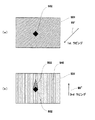
図24(b)に示すように、ツイスト配向した液晶分子4”に隣接した液晶分子4’を考える。液晶分子4”のツイスト角は60度であるとする。液晶分子4’は電圧が印加されない状態では、図24(a)に示すようにスプレイ配向している。一方、液晶分子4’は、電圧が印加されるとその電圧によって変形しようとする。この場合、液晶分子4’はツイスト配向した液晶分子4”に隣接しているため、セル厚方向84の変形だけではなくツイストするようにも変形しようとする。さらに、この場合、液晶分子4’は、ある電圧(約2.1V)まではツイスト変形よりセル厚方向84の変形の方が容易であるが、当該電圧以上になるとセル厚方向84の変形よりツイスト変形の方が容易になる。従って、当該電圧以上の電圧が印加されると液晶分子4’は、図24(d)に示すようにツイストする。このとき、液晶分子4’は電圧を印加しないときの回転方向と逆方向に300度ツイストする。このツイストしつつある液晶分子4’、例えば180度ツイストした液晶分子4’を断面方向から見ると、図24(c)に示すようにベンド配向に似ている。それ故、このツイストした状態からベンド配向へは容易に転移すると考えられる。
【0327】
ここで、液晶分子4’がセル厚方向84の変形よりツイスト変形の方が容易になる電圧は、スプレイ配向からベンド配向へ直接転移するための電圧より低い。そのため、液晶分子4’は低い電圧でスプレイ−ベンド転移する。そして、この転移した液晶分子4’が核となってスプレイ−ベンド転移が進行するため、スプレイ−ベンド転移が容易に行われるのであると考えられる。
【0328】
次に、上記効果を具体的に説明する。図25は液晶表示素子Eを転移させるために用いた転移電圧の波形を示す図である。液晶表示素子Eに、図25に示す、15Vの電圧値及び0.5秒のパルス幅を有する1パルスの方形波電圧を印加したところ、液晶表示素子Eはスプレイ配向からベンド配向に転移した。本件発明者の検討では、従来、25V程度の転移電圧が必要であった。従って、従来に比べると、液晶表示素子Eは、著しく低い電圧でかつ極短時間で転移させることが可能であることが判る。また、図25の波形の電圧を複数回かけてもよい。また、この波形の電圧を用いると、−10℃の温度でも確実に転移させることができた。
【0329】
図26は転移電圧に対する転移核発生率の変化を示す図である。図26では、転移電圧を変化させた場合の画素における転移核の発生率の変化を、−10℃、0℃、25℃(室温)、50℃の各温度について示している。図26によれば、温度に拘わらず、転移電圧が約10V以上で転移核発生率が100%となっている。従って、液晶表示素子Eは、転移電圧が約10Vであれば、画素毎に転移が確実に行われ、画素単位の点欠陥の発生を防止することが可能であることが判る。また、4Vで転移核が発生するため、時間さえかければ4Vの転移電圧で転移させることが可能であることが判る。
【0330】
次に、本実施の形態に係る液晶表示装置の変形例を説明する。
【0331】
上記構成では、複合柱スペーサを図21に示す形態を有するものとしたが、複合柱スペーサの形態は、これに限らず、図27に示すようなものであってもよい。図27は複合柱スペーサの変形例を示す平面図である。図27(a)、(b)の複合柱スペーサ203は単独の柱スペーサからなり、該柱スペーサはラビング方向69に垂直な辺を有する断面形状を有している。柱スペーサ203のラビング方向に垂直な辺204付近では実際にラビングされる方向(配向処理方向)が左右に分かれるため、この辺204の付近に転移の核が発生し、それにより転移が高速に発生する。図27(c)の複合柱スペーサ203は、各柱スペーサが同一の菱形断面形状を有している点でのみ、図22の複合柱スペーサと異なっているものである。図27(d)の複合柱スペーサ203は、三角形の断面形状を有する柱スペーサからなっている。本実施の形態の柱スペーサは、基本的に、配向処理方向を制御するように、ラビング方向69に対し斜め方向又は横方向に傾斜を有する断面形状を有していればよい。図27(e)の複合柱スペーサ203は、図27(c)の複合柱スペーサが横方向に連続して繰り返されるように構成されたものである。このような構成とすると、ラビングが左右からぶつかる領域205が数多く形成されるため、当該領域205に左回りツイストの領域と右回りツイストの領域とが接する箇所が有効に形成され、それにより転移核が発生しやすくなる。図27(f)の複合柱スペーサ203は、菱形断面形状を有する4個の柱スペーサが、ラビング方向69に平行な対角線を有する仮想の菱形の各頂点に位置するように配置されたものである。また、図21、図27(a)〜図27(f)においてラビング方向を逆にしてもよい。
【0332】
また、上記構成では、複合柱スペーサ203を補助容量電極65上に形成したが、図28に示すように、複合柱スペーサ203を画素電極64上に形成してもよい。
【0333】
また、上記構成では、複合柱スペーサ203を、TFT基板202上にその凹凸を利用して形成したが、図29に示すように、複合柱スペーサ203を、カラーフィルタ基板201に、カラーフィルタ76の段差を利用して形成してもよい。カラーフィルタ76の段差は、例えば、R,G,Bのそれぞれのカラーフィルタを形成する際に、ブラックマトリクス67上で各カラーフィルタ層を重ね合わせたり重ね合わせないようにしたりすることにより形成することができる。
【0334】
また、上記構成では、TFT基板202の、複合柱スペーサ203が形成される箇所を低くすることによって、複合柱スペーサ203を相手方の基板201に当接しないようにしているが、図30に示すように、カラーフィルタ基板201内面の、複合柱スペーサ203の先端に対向する部分に凹部86を形成することによって、該複合柱スペーサ203がカラーフィルタ基板201に当接しないようにしてもよい。凹部86は、フォトリソグラフィー法を用いて、ガラス基板1上にフォトレジスト層20を形成してそれに凹部72を設け、それらの上に対向電極2、配向膜3を順に形成することにより、形成することができる。なお、本図では複合柱スペーサ203が画素電極64上に形成される場合を示しているが、複合柱スペーサ203が補助容量電極65上に形成される場合にも、同様に凹部86を形成することができるのはいうまでもない。また、複合柱スペーサ203がカラーフィルタ基板201に形成される場合には、TFT基板202内面の、複合柱スペーサ203の先端に対向する部分に凹部を形成することによって、該複合柱スペーサ203がTFT基板202に当接しないようにすることができる。この場合の凹部も上記と同様に形成することができる。
【0335】
また、上記構成では液晶表示素子Eを、アクティブマトリクスタイプのもので構成したが、本実施の形態の本質は、基板にラビング制御用の複合柱スペーサを設けることにあるので、基本的に基板の種類は問わない。よって、パッシブマトリクスタイプ等、他のタイプのものにも本発明を同様に適用することができる。
実施の形態3
本発明の実施の形態3は、柱スペーサを有する液晶表示素子において、柱スペーサを、相手方の基板に接触していないものを含むように構成したものである。
【0336】
実施の形態2では、複合柱スペーサ203が、相手型の基板に接触していないものを含むように構成されているが、このように相手方の基板に接触していない柱スペーサを形成することは、転移核を形成する場合に限られるものではない。つまり、この構成は、本発明のように多数の転移核を形成する場合に必須の構成ではあるが、通常の、数画素に1個づつ柱スペーサを形成する場合にも有効である。一般に、スペーサビーズを基板間にばらまく場合には、スペーサビーズの粒径分布が存在するため、基板の弾性的な変形が有効に行われる。しかし、一般に、柱スペーサを形成した場合には、その高さは均一になってしまう。そのため、低温気泡が発生しやすい。そこで、柱スペーサ自体の高さは一定にしながらも、基板に凹凸をつけ、基板の凹凸によって柱スペーサの実効的な高さの分布を形成すると、室温近傍で基板に接触している柱スペーサの個数が低減され、この低温気泡の問題を解決することができる。本実施の形態の本質は、室温近傍で相手方の基板に接触していない柱スペーサが存在するということである。
実施の形態4
本発明の実施の形態4は、実施の形態2と異なり、複合柱スペーサ203を一部の画素にのみ設けたものである。図31において、符号73は、ブラックマトリクス、カラーフィルタ、対向電極等からなる層を示し、符号75は、ソース線、ゲート線、画素電極、補助容量電極、絶縁層等からなる配線層を示す。TFT基板202では、上記配線層75の表面を覆うようにアクリル系レジスト等の樹脂材料からなる平坦化層74が形成され、該平坦化層74上に複合柱スペーサ203(図には1個のみ示している)が形成されている。複合柱スペーサ203は一部の画素63にのみ設けられている。その他の点は実施の形態2と同様である。複合柱スペーサ203を一部の画素にのみ設けると、複合柱スペーサ203の周囲で発生したスプレイ−ベンド転移が画素63間に亘って成長する必要があるが、そのためには、基板201,202の表面が平坦であることが必要である。しかし、通常のアレイ基板(ここではTFT基板)202では、場合によっては配線層75に最大1μm程度の凹凸75aが存在する。そこで、本実施の形態では、平坦化層74を形成してその樹脂材料により配線層75表面の凹凸75aを相殺し、それによりアレイ基板202内面の凹凸を低減したものである。これにより、スプレイ−ベンド転移が画素間に亘って容易に成長した。
実施の形態5
本発明の実施の形態5は、光配向によって、局所的に、周囲の領域の配向処理方向と異なる方向に配向処理された領域を形成したものである。本発明の本質は、ツイスト配向領域を形成することにあるので、基本的に配向処理の方法は問わない。よって、光配向によってツイスト配向領域を形成しても、本発明の効果を得ることができる。例えば、図22に示されるような配向処理を光配向によって施すことにより、実施の形態2と同様の効果を得ることができる。但し、光配向処理を施す方の基板は、配向膜を光配向膜で構成する必要がある。その他の点は実施の形態2と同様にすればよい。
実施の形態6
本発明の実施の形態6は、実施の形態2に係る液晶表示素子を用いて液晶表示装置を構成したものである。
【0337】
図32に示すように、本実施の形態に係る液晶表示装置301は、実施の形態2に係る液晶表示素子Eと、液晶表示素子Eを駆動するソースドライバ305及びゲートドライバ304と、ソースドライバ305に基準電圧を供給する基準電源回路303と、映像信号307を入力されてこれをソースドライバ305に出力するとともに、基準電源回路303、ゲートドライバ304、及びソースドライバ305を制御するコントローラ302とを含んで構成されている。従って、転移専用の電源を備えてはいない。
【0338】
次に、以上のように構成された液晶表示装置301の転移動作を説明する。実施の形態2で述べたように、液晶表示素子Eは、4V以上の転移電圧を印加すれば転移する。但し、転移時間は転移電圧に依存する。一方、本実施の形態に係る液晶表示装置301の駆動電圧は最大6Vである。よって、この駆動電圧が印加されれれば液晶表示装置Eは転移する筈である。そこで、実際に、液晶表示装置301をオンさせると、液晶表示装置Eは上記駆動電圧が印加されているだけであるが転移した。また、液晶表示装置Eは、液晶表示装置301のオン後は通常の映像信号が流れつづけるが、それだけで10秒後にはほぼ転移が終了した。つまり、本実施の形態に係る液晶表示装置301は、図25に示すような特殊な波形や駆動電圧より高い電圧値を有する転移用の電圧を印加せずとも、通常の駆動波形と6Vの最大電圧値とを有する駆動電圧を印加しつづけることにより液晶表示素子Eを転移させることができる。そのため、転移専用の電源を備える必要がなく、コストを大きく低減することができる。
【0339】
なお、上記構成では液晶表示素子は、4Vで転移するもので構成されているが、液晶表示装置における液晶表示素子の駆動電圧は最大10V程度であるので、液晶表示素子は、10V以下で転移するものであればよい。
実施の形態7
本発明の実施の形態7は、液晶表示装置が転移専用の電源を備えたものである。すなわち、図33に示すように、本実施の形態に係る液晶表示装置308は、実施の形態6とは異なり、液晶表示装置として実施の形態4に係る液晶表示素子Fを備えている。液晶表示素子Fのカラーフィルタ基板及びTFT基板に一対の転移電圧印加用電極310が配設され、該一対の転移電圧印加用電極310の一方の電極上に、図31に示す複合柱スペーサ203が形成されている。また、該一対の転移電圧印加用電極310は、転移電圧印加回路306に接続され、該転移電圧印加回路306はコントローラ302によって制御されている。その他の点は、実施の形態6と同様である。
【0340】
以上のように構成された液晶表示装置308では、映像の表示に先立ち、コントローラ302の制御により一対の電極310に所定の転移電圧が印加され、それにより、液晶表示素子Fが転移する。その際、液晶表示素子Fは、局所的にツイスト配向領域が形成されているため、従来より低い電圧でかつ短時間に転移する。
実施の形態8
上記実施の形態2では、ラビング方向を局所的に制御することによってスプレイ−べンド転移を確実化することができた。本発明の実施の形態8は、この転移過程をより詳細に検討し、その結果、転移核の生成を確実化したものである。
【0341】
図34は液晶表示素子における液晶の安定条件を示す概念図であり、(a)は基本的な液晶の安定条件を示す図、(b)はパラレル配向及びツイスト配向における液晶の安定条件を示す図である。また、図35は、局所的にツイスト配向領域が形成された液晶表示素子におけるスプレイ−ベンド転移の過程を模式的に示す概念図であり、(a)は互いに逆方向の2つのツイスト配向領域が相接する場合を示す図、(b)は一方のツイスト角が90度である場合を示す図、(c)は一方のツイスト角が90度以上である場合を示す図、(d)は互いに同方向の2つのツイスト配向領域が相接する場合を示す図である。
【0342】
図34(a)に示すように、基本的に液晶は、基板に対する傾斜角度が変化しない通常配列状態を好み、またツイスト変形が少ない状態を好む。
【0343】
しかし、この2つの条件が相反する状態がパラレル配向状態に代表されるものである。また、ツイスト角が90度以下の配向においても、液晶の安定条件は、基本的にはパラレル配向状態と同じである。図34(b)に示すように、電圧を印加していない状態では、パラレル配向状態では、ツイスト角が0度のスプレイ配向がエネルギ的に安定である。しかし、約2V以上の電圧を印加すると、エネルギ的には、ツイスト角が180度の通常配列が安定になる。電圧印加によって180度ツイストが安定な状態になるとこの状態からすぐにべンド配向に連続的に転移することは確認された。従って、この180度ツイスト状態を過渡的に形成することが必要である。しかしながら、電圧印加によって180度ツイスト状態がエネルギ的に安定になっても、実際には容易に180度ツイストには変化しない。これは構造変化が大きいため、この転移のための核が必要となるからである。本発明のポイントは、この転移核をいかに確実に形成するかにある。なお、ツイスト角が90度以下のスプレイツイスト配向においても、約2V以上の電圧を印加したときにエネルギ的に安定になるツイスト角が180度−θ(θはツイスト角)である他は、基本的にパラレル配向と同様である。
【0344】
図35(a)は、実施の形態2で示したような、複合柱スペーサを形成した場合を示す図である。このときには、以下の過程を経て転移が発生する。
【0345】
図35(a)に示すように、右回りツイスト状態(ツイスト角=−60度)の領域403と左回りツイスト状態(ツイスト角=75度)の領域402が形成され、それらが互いに接触している揚合を考える。符号401はパラレル配向領域を示し、白色矢印はラビング方向を、有色矢印は液晶分子の方向をそれぞれ示す。電圧が印加されると、例えば初期に右回りツイストであった領域403は左回りツイストでツイスト角が大きい状態が安定になる。ところが、核がないとこの状態に転移できない。しかしながら、右回りツイストであった領域403は、当初から左回りツイストの領域402が接していればその領域402が核になって左回りツイストに転移し、通常配列ツイスト404が発生する。このため、右回りツイスト領域403と左回りツイスト領域402との間にはデフェクトが観察され、それがどちらかの領域の方向に移動することが観察された。
【0346】
さらに、外側のパラレル配向領域401と、ツイスト角の大きな通常配列ツイスト404が接してくるため、この通常配列ツイスト404が核になって外側のパラレル配向領域401にべンド転移405が発生した。
【0347】
このように、右回りのツイスト領域403と左回りのツイスト領域402とが接していると、そこを核にして転移が発生することが見出された。また、このツイスト角は90度以下であれば転移電圧を低くすることができた。例えば、ツイスト角が90度の場合は、転移電圧は5Vであり、60度の場合は8Vであった。但し、図35(d)に示すように、同じ回転方向のスプレイツイストを2種類形成しても転移核形成への寄与は少なかった。
【0348】
さらに、ツイスト角を大きくして検討した。図35(b)に示すように、相接する2つのツイスト領域402,406のうちの一方の領域406のツイスト角が90度の場合は、その領域406に相反する方向の2つのツイスト状態が初期より混在しており、電圧を印加すると片方の通常配列ツイスト404が成長し、これが外側のパラレル配向領域401と接触すると、その接触箇所を核にべンド転移405が発生した。
【0349】
また、図35(c)に示すように、相接する2つのツイスト領域402,407のうちの一方の領域407のツイスト角が90度以上(ここでは105度)の場合は、初期より通常配列ツイスト404が安定であり、これを核にしてべンド転移405が発生した。従って、結果的に、90度又は90度以上のツイスト角の領域を形成する場合には、2種類のツイスト領域を形成する必要はなかった。ただし、転移に要する電圧は、ツイスト角が90度の場合に5V、105度の場合に7Vと大きくなる。
【0350】
次に、上記のようなツイスト配向領域の形成方法を説明する。図35(a)に示すように、パラレル配向領域中に相接する右回りツイスト領域と左回りツイスト領域とを局所的に形成することは、実施の形態2で述べたように、基板上に複合柱スペーサを形成してラビングを施すことにより実現することができる。
【0351】
一方、図35(b)、図35(c)に示すように、パラレル配向領域中にツイスト角が90度以上のツイスト配向領域を形成することは、これまでの実施の形態で述べたような1回の配向処理で実現することは不可能であった。そこで、本件発明者は、柱スペーサを形成した基板に2回のラビングを施すことによりこれを実現した。これを図36を用いて具体的に説明する。
【0352】
図36は本実施の形態に係る液晶表示素子の一方の基板の配向処理を模式的に示す平面図であって、(a)は1回目のラビングを施した後の状態を示す図、(b)は2回目のラビングを施した後の状態を示す図である。図36(a)に示すように、柱スペーサ502が形成された基板501を、基準方向、つまり液晶を挟む一対の基板の全体的な配向処理方向(図21の符号69で示す方向)に対し90度以上(ここでは左回りに約135度)傾斜した方向69’に1回目のラビングを施し、その後、図36(b)に示すように、上記基準方向69”に2回目のラビングを施した。すると、柱スペーサ502の影領域503では、2回目のラビングがなされないため、1回目のラビングによる配向処理が残存した。これにより、パラレル配向領域540中にツイスト角が90度以上のツイスト配向領域503を形成することができた。
【0353】
また、このようなツイスト角が90度以上のツイスト配向領域を形成するのに、液晶に若干のカイラル剤を添加することも有効であった。つまり、一般にカイラル剤を添加しないとツイスト角が90度以上のツイスト配向領域を形成することは困難である。これは、複数回のラビング処理を行なっても同じである。しかし、前述したようにツイスト角が90度以上のツイスト配向領域を形成するとそれが転移核になる。そこで、カイラル剤を添加すると特定の回転方向の配向状態が安定になる。例えば、右回りのカイラル剤を添加すると右回りのツイスト配向領域が安定になり、たとえツイスト角が90度以上のツイスト配向領域でも安定に存在することができる。このようにカイラル剤はツイスト角が90度以上のツイスト配向領域を形成する場合に有効であった。
【0354】
以上の方法で配向処理された基板を用いて、実施の形態2で述べたような液晶表示素子を作成すると、スプレイ配向からベンド配向への転移核が確実に生成されるため、スプレイ−ベンド転移がより容易な液晶表示素子を得ることができる。
実施の形態9
本発明の実施の形態9は、配向膜にキズを形成することにより、相接する異種の異配向方位領域を形成したものである。
【0355】
図37は、本実施の形態に係る液晶表示素子の一方の基板の配向処理を模式的に示す平面図である。
【0356】
図37において、本実施の形態に係る液晶表示素子の一方の基板501は、表層部に配向膜(図示せず)が形成され、該配向膜の表面に、ラビング方向69に湾曲するようにキズ504が形成されている。このキズ504は、本実施の形態では、基板501の表面に針を立てて図示するような形状に引っかくことにより形成した。もちろん、このキズ504を形成する方法はこれに限るものではなく、例えば、レーザを基板504の表面にパルス的に照射して配向膜を除去することによりキズ504を形成してもよい。
【0357】
このような構成とすると、他方の基板にパラレル配向処理を施すことにより、基板501のキズ504上に位置する液晶分子は、図中の矢印で示されるような方向に配向する。つまり、キズ504中には、その中央部を境に左回りツイストの領域506と右回りツイストの領域505とが形成されている。このように左回りツイストの領域506と右回りツイストの領域505とを互いに接するように形成すると、実施の形態8で述べたように転移核を確実に生成することができる。本実施の形態では、左回りツイストの領域506と右回りツイストの領域505との境界部より転移が発生し、より容易にスプレイ−ベンド転移を行うことができた。
【0358】
なお、ここで、キズとは配向膜が部分的に欠落している状態を指す。このキズを形成するために、フォトレジストを用いてエッチングで除去してもよい。また特定の溶媒に溶解する液と非溶解性の液とを混合しエマルジョン化して硬化し、その後、一方を前記溶媒で除去してもよい。
実施の形態10
本発明の実施の形態10は、局所的な配向処理を光配向で行うことにより、ツイスト角が90度以上のツイスト配向領域を形成したものである。
【0359】
図38は本実施の形態に係る液晶表示素子の一方の基板の配向処理を模式的に示す平面図である。
【0360】
図38において、本実施の形態に係る液晶表示素子の一方の基板501は、表層部に光感応基を有する配向膜(図示せず)が形成され、該配向膜の表面に、全体的なパラレル配向領域541の中に、ツイスト角が90度以上の円形のツイスト配向領域508が点在するように、配向処理が施されている。ツイスト配向領域508のツイスト角は、本実施の形態では左回りに約135度である。円形のツイスト配向領域508は、基板501上のブラックマトリクスに対応する部分に形成した。
【0361】
この配向処理は、以下のように行った。まず、基板501の表層部に光感応基を有する配向膜を形成し、その後、該配向膜の全面に、配向方向が基準方向(実施の形態8図36の説明参照)507となるよう、偏光紫外線を照射して配向処理を施した。次いで、この偏光紫外線による配向処理を行った基板501の表面上のブラックマトリクスに対応する部分の、複数の円形の領域508に、偏光レーザを照射した。この偏光レーザの照射は、配向方向509が、基準方向507に対し、左回りに約135度傾斜するように行った。これにより、ツイスト角が90度以上の局所的なツイスト配向領域508を形成した。なお、このツイスト配向領域508は、パルスレーザを走査させながら照射することにより形成してもよい。また、ツイスト配向領域508に対応する開口を有するマスクで基板501の表面を覆い、そのマスクの上から偏光紫外線を照射することにより形成してもよい。
【0362】
このような構成とすると、他方の基板にパラレル配向処理を施すことにより、液晶表示素子は、ツイスト角が90度以上のツイスト配向領域を有することとなるので、実施の形態8で述べたように転移核を確実に生成することができ、その結果、より容易にスプレイ−ベンド転移を行うことができる。
実施の形態11
本発明の実施の形態11は、転移の核の望ましい密度を示したものである。
【0363】
すなわち、本発明の本質は、転移の核を形成することにある。但し、基板上に凹凸があると、転移がこの凹凸で停止する場合が往々にしてある。そこで、転移核をより多く形成することが転移を確実化するために重要である。埋想としては、転移の核を各画素に形成することが望ましい。
【0364】
ここで、実用性を考慮すると、この転移核(正確には、転移核となる異配向方位領域を形成するための立体障害)が柱スペーサを兼用するのが望ましいが、その一方、各画素に柱スペーサからなる転移核を形成すると、柱スペーサが過剰になるという問題があった。この問題は、基板に設けた凹凸を利用して相手方基板に当接する柱スペーサを減少させることにより解決した。これについては実施の形態2で述べた。従って、この方法によれば、特に問題を生じることなく転移核を各画素に形成し、それにより理想的な転移核の密度を実現することができる。
【0365】
しかしながら、もし転移核が少なくて済むのであれば、製造コストを低減することができるので、それに越したことはない。そこで、さらに検討を重ねた結果、転移核の密度に関して以下のことが判明した。
【0366】
すなわち、第1に、本発明の効果を得るためには、各画素に転移核を形成する必要はないが、100画素に1以上の密度で転移核を形成することが望ましい。
【0367】
第2に、10画素に1以上の密度で転移核を形成すると、ほぼ確実にパネル全体を転移させることができる。
【0368】
第3に、本実施の形態を含めこれまでの実施の形態では、転移核を基板上に周期的に形成したが、必ずしも周期的に形成する必要はない。むしろ、転移核を基板上に周期的に形成すると、フォトリソグラフィー法を用いてパネルを作成する際に転移核形成用パターンがずれた場合、完成した液晶表示素子の表示動作の際に画像がモアレのように見える場合があるという問題が生じた。しかし、転移核を基板上にランダムに形成してこの転移核形成用パターンをランダムにすることにより、この問題を解決することができた。
【0369】
本実施の形態に係る液晶表示素子は、上記第1〜第3の条件を満たすように構成してなるものである。
実施の形態12
実施の形態11で述べたように、画素間の転移の成長が基板上の凹凸で停止する場合があるが、本発明の実施の形態12は、この画素間の転移の成長を阻害しない又は促進するために、転移核をソース線上に形成したものである。
【0370】
図39は本実施の形態に係る液晶表示素子のアクティブマトリクス基板の構成を模式的に示す平面図である。
【0371】
図39において、本実施の形態では、アクティブマトリクス基板202に、複数(ここでは3つ)の立体障害510が、ソース線62を跨ぐようにソース線62の延在方向に所定間隔で列設されている。各立体障害510は、平面視において、両端がソース線62を挟む2つの画素電極64に掛かるように形成されている。また、各立体障害510は、アクティブマトリクス基板202上に立設された矩形の板状の突起で構成されている。本実施の形態ではラビング方向69は図示するようにソース線62の延在方向であり、各立体障害510は、ラビングの影が連続して発生するように近接して配置されかつラビングが流れやすいようにラビング方向69に対し斜めに配置されている。これ以外の点は、実施の形態4と同様である。
【0372】
このように構成された液晶表示素子では、立体障害510によって、デフェクト、特に2種類のスプレイ配向状態間のデフェクト(一方の基板近傍にスプレイ配向中心を有する領域と他方の基板近傍にスプレイ配向中心を有する領域の境界)がトラップされ、そこを起点にして転移の画素間への成長が促進されることが確認された。本実施の形態に係る発明で根幹になるのはデフェクトを保持する機構である。
【0373】
なお、実施の形態4で詳述したように、転移の画素間の成長を促進する手段として、基板上の凹凸を低減することも有効である。転移の画素間の成長を阻害しているものは基板の凹凸であるから、これを樹脂層による平坦化層によって低減させることでさらに転移の画素間の成長を促進させることができる。
実施の形態13
本発明の実施の形態13は、ラビングを制御するための立体障害を、柱スペーサを用いずに、アレイ基板におけるアレイ構造の段差を用いて形成するようにしたものである。
【0374】
本実施の形態においては、アレイ基板のアレイを形成する過程において、最大2μmの段差を形成することができた。そして、そのアレイ基板に配向処理を施す際に、この最大2μmの段差を利用してラビングを制御することにより転移核(異配向方位領域)を形成することができた。
【0375】
このように作成したアレイ基板を用いた液晶表示素子では、柱スペーサを用いた場合に比べると、スプレイ配向からベンド配向へ転移する確率は低下した。しかし、本発明の転移核を有する液晶表示素子を得るのに、アレイ基板の製造にー般に用いるアレイプロセスの変更だけで済むため、転移核を容易に形成できるメリットがある。また、本実施の形態に係る配向処理方法を、実施の形態8で述べた、異なる配向方向に2度ラビングする配向処理方法と組み合わせることにより、ベンド転移を確実化する効果を一層高めることができた。
実施の形態14
本発明の実施の形態14は、異配向方位領域を形成するために柱スペーサ(立体障害)を撥水性にしたものである。
【0376】
図40は本実施の形態に係る液晶表示素子の基板の配向処理の状態を模式的に示す平面図である。
【0377】
図40において、基板202上には、複合柱スペーサ203が形成され、その各柱スペーサ203A,203B,203Cは撥水性の材料からなっている。ここで、一般に、柱スペーサ203A,203B,203Cの周辺、特に、そのラビング方向69において奥側に位置する部分は、ラビングされ難い。そこで、柱スペーサ203A,203B,203Cを撥水性にすると、該柱スペーサ203A,203B,203Cの周辺に位置する液晶分子は、図示するように、該柱スペーサ203A,203B,203Cの側面に対し垂直な方向511に配向する傾向を有する。これにより、柱スペーサ203A,203B,203Cの周辺に、右回りツイスト領域と左回りツイスト領域とが相接するように形成されるので、その接触箇所がべンド転移の核として作用する。従って、このように配向処理された基板202を用いた本実施の形態に係る液晶表示素子は、転移核が確実に生成され、より一層ベンド転移を確実化することができる。
【0378】
なお、基板202上に柱スペーサ203A,203B,203Cを形成する際には、まず、撥水性材料からなる柱スペーサ203A,203B,203Cを形成し、次いで、それらが形成された基板表面を覆うように配向膜を塗布する。すると、柱スペーサ203A,203B,203Cの表面に塗布された配向膜ははじかれ、該柱スペーサ203A,203B,203Cは撥水性の表面が露出する。これにより、基板202上に撥水性の表面を有する柱スペーサ203A,203B,203Cを形成することができる。
【0379】
また、本実施の形態で重要なのは、基板上にラビング処理がされていない、又はラビング処理が非常に弱い領域を形成することと、その領域に位置する液晶分子を所定の方向に配向させる他の配向手段を有することである。本実施の形態では、この他の配向手段は柱スペーサの撥水性である。
実施の形態15
本発明の実施の形態15は、基板の表示域の周辺部に形成した柱スペーサも基板間隔を保持するスペーサとして機能するようにしたものである。
【0380】
本発明は転移核を生成してベンド転移を確実化するものであり、実施の形態2では、その転移核として柱スペーサを用い、その柱スペーサを補助容量電極上に形成した。ところで、アクティブマトリクスタイプの液晶表示素子では、TFT基板の補助容量が形成される部分は、該TFT基板側の画素部分に比べアレイ構造物によって1μm程度高くなっている。また、力ラーフィルタ基板の補助容量が形成される部分もブラックマトリクスが形成されているため、これも該カラーフィルタ基板の画素部分より高くなっている。このため、補助容量が形成される部分に形成した柱スペーサは、両方の基板に接触するため基板間隔を保持するスペーサとして機能する。しかし、パネルの表示域の外側の領域に形成された柱スペーサは、当該領域にアクティブマトリクスの段差が形成されていないため、基板間隔を保持するスペーサとして機能せず、そのため、パネルの表示域の外側でセル厚が薄くなるという問題があった。
【0381】
この間題の解決策として、アクティブマトリクスの段差に相当する段差を補償するために、TFT基板の表示域の外側に形成するシール樹脂層の内部に所定サイズのガラスファイバー等からなるスペーサを混入させることも考えられる。しかし、そのようにすると、そのスペーサによって信号配線が傷つく可能性がある。
【0382】
そこで、本実施の形態では、この問題を解決すべく以下のような構成としている。
【0383】
図41は本実施の形態に係る液晶表示素子の構成を模式的に示す断面図である。図41において図20と同一符号は同一又は相当する部分を示す。また、図41では、カラーフィルタ基板201、TFT基板202ともに、図示する要素以外の要素を省略し、簡略化して描いてある。
【0384】
図41に示すように、本実施の形態に係る液晶表示素子Gでは、TFT板基板202の表示域542と該表示域542の周辺部に柱スペーサ203が形成され、表示域542の周辺部に位置する柱スペーサ203’は表示域542の周辺部に形成されたダミーパターン512上に形成されている。ダミーパターン512の高さは、表示域542内の柱スペーサ203が形成されている箇所543と同じ高さとなっている。なお、符号543で示される箇所は、柱スペーサ203が形成される箇所を模式的に示したもので、その高さはアクティブマトリクスの段差に相当している。また、ダミーパターン512は、本実施の形態ではフォトレジストで構成したが、配線材料や絶縁膜で構成してもよい。
【0385】
このような構成とすると、TFT基板202の表示域542の周辺部に形成された柱スペーサ203’も、表示域542内に形成された柱スペーサと同じ高さを有するので、基板201,202の間隔を保持するスペーサとして機能する。
【0386】
なお、TFT基板202の表示域542の周辺部に形成される柱スペーサ203’及びダミーパターン512のいずれか又は双方をカラーフィルタ基板201に設けてもよい。また、実施の形態2で示したように、表示域542の周辺部のダミーパターン512にも高低をつけ、柱スペーサの数が過剰になるのを防止してもよい。また、
表示域542の周辺部の柱スペーサ203’の密度を表示域542内の柱スペーサの密度より下げてもよい。
実施の形態16
本発明の実施の形態16は、横方向(基板に平行な方向)の電界(以下、横電界という)を印加することにより、異配向方位領域を形成するようにしたものである。
【0387】
図42は本実施の形態に係る液晶表示素子の構成を模式的に示す図であって、(a)は断面図、(b)は平面図である。また、図43は、図42の液晶表示素子に印加される駆動電圧の波形を示すグラフである。図42、図43において図20と同一符号は同一又は相当する部分を示す。
【0388】
実施の形態2では、ラビングの方向を制御して異配向方位領域を形成したが、本実施の形態では、実施の形態2とは異なり、電界によって異配向方位領域を形成する。この異配向方位領域を形成する期間は転位電圧が印加されている期間だけでよい。
【0389】
図42(a)、(b)に示すように、本実施の形態に係る液晶表示素子では、TFT基板202の画素電極64及びゲート線61の相隣合う縁部が、互いに噛み合うようなジグザグ形状544にそれぞれ形成されている。上記画素電極64及びゲート線61の相隣合う縁部はラビング方向69に対し直角な方向に延びるように形成され、かつ交互に反対方向に傾斜するように延びて上記ジグザグ形状544を形成する2種類の傾斜直線544a,544bは、本実施の形態では、ラビング方向69に対し±約45度の角度をなすように形成されている。また、上記ジグザグ形状544のピッチPは、本実施の形態では、100μmとした。このピッチPは、30μm以上であれば後述する効果を奏し、また、画素電極64のピッチよりも小さいことが望ましい。また、上記画素電極64及びゲート線61の相隣合う縁部同士の間隔は、本実施の形態では、10μmとした。この間隔は、小さい方が横電界が強くなり、効果的であるが、エッチングが困難になる。この間隔は、4μm以上であれば後述する効果を奏するが、20μm以下とするのが望ましい。
【0390】
そして、ゲート線61と画素電極64との間に所定の電圧が印加され、それにより横方向の電界513が発生する。これ以外の点は、実施の形態2と同様である。
【0391】
次に、この所定の電圧について図42及び図43を用いて説明する。図42、図43において、ゲート線61には通常の駆動波形の電圧(ゲート電圧)516が印加される。このゲート電圧516は、+数Vのハイレベルの期間と−20Vのローレベルの期間とを有する矩形波からなり、該ローレベルの期間が画素のOFF期間であるので、ゲート線61にはほとんどの期間に亘って−20Vが印加される。また、画素電極64の電位(画素電圧)514、すなわちソース線の電位は、+3Vに保持される。さらに、転移電圧は主に対向電圧515を振ることで得ることとし、対向電圧515の波形を、+3Vのハイレベルの期間と−25vのローレベルの期間とを有する周波数0.5Hzの矩形波とした。これにより、ゲート電圧516がローレベルである期間に画素電極64とゲート線61との間に23Vの電圧が印加され、横電界513が発生する。この横電界513の方向は、画素電極64からゲート線61に向かう方向である。また、対向電圧515がローレベルである期間に、対向電極と画素電極64との間に28V、対向電極とゲート線61との間に5Vの転移電圧がそれぞれ印加され、この転移電圧と上記横電界513とは、対向電圧515及びゲート電圧516が共にローレベルである期間545に同時に印加される。
【0392】
次に、以上のように構成された液晶表示素子の動作を説明する。図42、図43において、液晶表示素子がオンされ、ゲート電圧516がローレベルになると、画素電極64とゲート線61との間に横電界513が発生し、その横電界513が存在する部分に位置する液晶分子の配向方位が該横電界513の方向に変化する。ここで、横電界513は、画素電極64及びゲート線61の相隣合う縁部のジグザグ形状544の2種類の傾斜直線544a,544bに直交する方向に発生する。よって、上記画素電極64及びゲート線61の相隣合う縁部同士の間隙部に、ラビング方向69に対し右回り及び左回りに約45度傾斜した横電界の領域が形成され、その横電界に応じてラビング方向69に対し右回り及び左回りに約45度ツイストした2種類のツイスト配向領域が交互にかつ相接するように形成される。次いで、対向電圧515がローレベルになると、対向電極と画素電極64との間に28V、対向電極とゲート線61との間に5Vの転移電圧がそれぞれ印加され、それにより、上記2種類のツイスト配向領域の接触部に転移核が生成され、その転移核が成長してベンド転移が行われる。よって、より一層確実にベンド転移を行うことができる。ここで、上記2種類のツイスト配向領域の接触部は、上記ジグザグ形状544の各頂点部分であり、該頂点付近から実際に転移が発生した。
【0393】
本実施の形態の本質は、画素電極とゲート電極との間に発生させる横電界によって、相接する右回りツイスト配向領域及び左回りツイスト配向領域を形成することにある。
【0394】
なお、上記左右のツイスト配向領域のツイスト角度は、上記ジグザグ形状544の各傾斜直線544a,544bのラビング方向69に対する角度、あるいは上記ジグザグ形状544の延在方向とラビング方向69との相対角度を選択することにより、所望の角度に設定することができる。
実施の形態17
図44は本発明の実施の形態17に係る液晶表示素子の構成を模式的に示す平面図である。また、図45は、図44の液晶表示素子に印加される駆動電圧の波形を示すグラフである。図44、図45において図42、図43と同一符号は同一又は相当する部分を示す。
【0395】
実施の形態16では、ゲート線と画素電極との間に横電界を発生させたが、本実施の形態は、実施の形態16と異なり、ソース線と画素電極との間に横電界を発生させるものである。
【0396】
図44に示すように、本実施の形態に係る液晶表示素子では、TFT基板202の画素電極64及びソース線62の相隣合う縁部が、互いに噛み合うようなジグザグ形状544にそれぞれ形成されている。この場合、ソース線62は対向する2つの縁部の各々に隣合う画素電極64’,64”の縁部とそれぞれジグザグ形状544で噛み合うように形成されている。この双方のジグザグ形状544,544は、本実施の形態では同一である。上記画素電極64及びソース線62の相隣合う縁部はラビング方向69に対し平行な方向に延びるように形成され、かつ交互に反対方向に傾斜するように延びて上記ジグザグ形状544を形成する2種類の傾斜直線544a,544bは、本実施の形態では、ラビング方向69に対し、それぞれ、約135度、及び約45度の角度をなすように形成されている。その他の点は実施の形態16と同様である。
【0397】
次に、駆動電圧について図44及び図45を用いて説明する。図44、図45において、互いに隣接するソース線、換言すれば、あるソース線62を挟む2つの画素電極64’,64”に、互いに逆極性(逆符号)の電圧が印加される。つまり、一方の画素電極64’には、+7Vのハイレベルの期間と−8Vのローレベルの期間とを有する所定周波数の矩形波からなる電圧(画素電圧514’)が印加され、他方の画素電極64”には該画素電圧514’と逆位相の矩形波からなる電圧(画素電圧514”)が印加される。そして、実施の形態16と同様、転移電圧は対向電圧515を振ることで得ることとし、対向電圧515の波形を、正電圧のハイレベルの期間と負電圧のローレベルの期間とを有する周波数0.5Hzの矩形波とした。
これにより、
図示するソース線62と、図示されない、該ソース線62に隣接するソース線に接続された画素電極64”との間に15Vの電圧が印加され、横電界513が発生する。この横電界513の方向は、ソース線62から画素電極64”に向かう方向である。また、対向電圧515がローレベルである期間に、対向電極と画素電極64との間に所定の転移電圧が印加される。
【0398】
このように構成された液晶表示素子では、液晶表示素子がオンされ、画素電圧514”がローレベルになると、画素電極64”とソース線62との間に横電界513が発生し、その横電界513が存在する部分に位置する液晶分子の配向方位が該横電界513の方向に変化する。これにより、実施の形態16で述べたように、画素電極64”及びソース線62の相隣合う縁部同士の間隙部に、2種類のツイスト配向領域が交互にかつ相接するように形成される。但し、本実施の形態では、この2種類のツイスト配向領域は、右回りに、それぞれ、約45度、及び約135度のツイスト角を有している。次いで、対向電圧515がローレベルになると、対向電極と画素電極64との間に所定の転移電圧が印加され、それにより、上記2種類のツイスト配向領域の接触部に転移核が生成され、その転移核が成長してベンド転移が行われる。よって、より一層確実にベンド転移を行うことができる。
【0399】
本実施の形態では、ツイスト角は上記の通り、約45度及び約135度であるが、このツイスト角が、45度以上であると転移が有効に発生し、60度以上であれるとさらに効果的であった。
【0400】
また、本実施の形態では、対向電圧の振幅で転移電圧を付与したが、対向電圧を一定にして、ソース電位の振幅で転移電圧を付与してもよい。
【0401】
また、実施の形態16、17ではジグザグ形状を直線で形成したが、これを曲線で形成してもよい。
実施の形態18
本発明の実施の形態18は、ラビング処理におけるバイアス角度を最適化することにより異配向方位領域を形成するものである。
【0402】
図46は本実施の形態に係る液晶表示素子の製造方法を示す模式図、図47は本実施の形態に係る液晶表示素子の基板の配向処理の状態を示す平面図である。
【0403】
図46において、ラビング用のローラ517には表面にラビング布(バフ布、図示せず)が巻かれている。一方、基板202の表面には配向膜(図示せず)が形成され図47に示す複合柱スペーサ203が形成されている。ラビング処理を行うには、まず、ローラ517を回転させ、次いで、基板202をローラ517に接触させながら該ローラ517の下方を通過させる。なお、ローラ517の回転方向は矢印518で示す方向である。これにより、基板202の配向膜はローラ517のラビング布によりラビングされる。この時、基板202のローラに対する移動速度はローラ517の周速に比べて無視し得る程小さいので、基板202のラビング方向69は、ローラ517の回転方向、すなわち、該ローラ517の回転軸に直角な方向になる。このラビング方向69と基板202のローラ517に対する移動方向591とのなす角度がバイアス角度Θである。本実施の形態ではこのバイアス角度Θを小さくした。また、ローラ517のラビング布の繊維を、実施の形態2の図22のラビングを行う場合に比べて剛直なものとした。
【0404】
この条件の下でラビングを行うと、図47に示すように、複合柱スペーサ203を構成する各柱スペーサ203A,203b,203Cのラビングの影部分519に、ラビング方向69から見て、右方向にラビングされる領域519a,519cと左方向にラビングされる領域519b,519dとができた。これは、柱スペーサ203A,203B,203Cをラビング布の繊維が乗り越える際、あるいは乗り越えた繊維が基板202に着地する際に横方向にずれるため、ラビング方向69に対して横方向の成分が発生し、該ラビング方向69に対し斜め方向にラビングされるのであると考えられる。これにより、相接する右回りツイスト配向領域519a,519cと左回りツイスト配向領域519b,519dとが形成され、それらの接触個所520から転移が発生した。その結果、ベンド転移をより一層確実化することができた。
【0405】
なお、バイアス角度Θが大きい場合には、右方向にラビングされる領域と左方向にラビングされる領域とのバランスが崩れてしまう。従って、バイアス角度Θは小さい方が好ましいが、バイアス角度が30度以下であれば、転移発生に関して良好な結果が得られた。
【0406】
また、本実施の形態におけるラビング処理結果は実施の形態2におけるラビング処理結果と異なっているが、本実施の形態は、ラビング布が柱スペーサを乗り越えるモードが支配的な場合である。そして、ラビング布の繊維が比較的剛直な場合にこのモードになる。一方、実施の形態2は、ラビング布が柱スペーサ間を流れるモードが支配的な場合である。そして、ラビング布の繊維が比較的柔軟な場合にこのモードになる。
実施の形態19
実施の形態2では補助容量電極上に柱スペーサを形成した。しかし、補助容量電極と画素電極との間には電極が存在しない隙間があり、そのため、ベンド転移の進行が阻害されることがあった。そこで本発明実施の形態19では、以下の構成としている。
【0407】
図48は本実施の形態に係る液晶表示素子の構成を模式的に示す平面図、図49は図48のXXXXIX−XXXXIX矢視断面図である。図48、図49において図19、図20と同一符号は同一又は相当する部分を示す。
【0408】
図48,図49に示すように、本実施の形態に係る液晶表示素子Hは、実施の形態2と異なり、補助容量電極65上に絶縁層77を介して画素電極64がオーバーラップしている。これ以外の点は実施の形態2と同様である。
【0409】
このような構成とすることにより、複合柱スペーサ203の周囲で発生したベンド転移に電界が途切れなく作用し、ベンド転移が良好に進行するようになった。
【0410】
また、本実施の形態に示すように、画素電極64が最上層に位置する構造とすると、補助容量電極65に画素電極65をオーバラップさせることが比較的容易である。
【0411】
さらに、上記ベンド転移の進行を促進するために、実施の形態4で述べたような平坦化処理を行っても良い。
実施の形態20
本発明の実施の形態20は、無電圧下で第1の配向状態になるとともに表示電圧下で第2の配向状態になり、該第1、第2の配向状態間にエネルギ障壁が存在する液晶を用いた液晶表示素子において、該第2の配向状態との間に存在するエネルギ障壁が上記第1、第2の配向状態間のエネルギ障壁より小さい第3の配向状態を液晶中に部分的に保存し、その保存された部分的な第3の配向状態を該液晶の全面的な第2の配向状態への転移の核として利用するものである。
【0412】
図50は本実施の形態に係る液晶表示素子の構成を模式的に示す平面図、図51は図50のXXXXXI−XXXXXI矢視断面図である。図50、図51において図19、図20と同一符号は同一又は相当する部分を示す。
【0413】
図50、図51に示すように、本実施の形態に係る液晶表示素子Iは、実施の形態2のラビング制御用の立体障害203(図19参照)に代えて、液晶層4の過渡的配向状態保存用の不完全囲繞体601を有している。この不完全囲繞体601は、本実施の形態ではTFT基板202に平行な面内にて周回するようにTFT基板202上に形成され、かつ、実施の形態2と同様、柱スペーサを兼用している。また、画素電極64は、絶縁層77を介して、補助容量電極65上にオーバラップしている。これ以外の点は、実施の形態2と同様である。ここで、本明細書において、不完全囲繞体とは、例えば、図52に示すように、全体として、ある面内にて周回するように三次元領域603を囲繞し、かつ一部に、該三次元領域603を囲繞していない欠落部602を有する立体構造物601をいう。
【0414】
次に、上記不完全囲繞体601について詳しく説明する。本実施の形態に係る液晶表示素子Iは、2枚の基板201,202間に液晶4を挟持し、その各基板201,202には透明電極64,79が形成されている。一方の基板202には、TFT66、及び補助容量電極65が形成されたアクティブマトリクス基板が、もう一方の基板201には画素63間にブラツクマトリクス67が形成された基板が用いられている。そして、このようなアクティブマトリクス素子の構造を通じて、液晶層4に電圧が印加される。
【0415】
本実施の形態においては、液晶表示素子Iに図53に示すようなステツプ状の波形の転移電圧を印加して、図54(a)に示すスプレイ配向4aから図54(b)に示すべンド配向4bへ転移させた。
【0416】
従来の液晶表示素子では、スプレイ配向からべンド配向への転移には多くの時間、例えば、数秒から数十秒の時間を要した。また、図53に示す波形の転移電圧を印加した後にも、スプレイ配向が残存し、画像の表示も不均一であった。
【0417】
本件発明者は、この転移時問を短縮しかつ確実化するために、鋭意、検討を進めた結果、以下の現象を見出した。
【0418】
すなわち、一旦、べンド配向に転移した後に印加電圧を瞬時にゼロVにすると、ベンド配向は図55に示すような180度ツイスト配向4cに一旦なることが判明した。この180度ツイスト配向4cは不安定であり、通常、数秒から数十秒後には液晶層全体がスプレイ配向に戻る。従来の液晶表示装置では、この180度ツイスト配向4cは残らず全て消滅した。
【0419】
このように、180度ツイスト配向が全て消失した後、すなわち、液晶パネル全面がスプレイ配向の状態で、再び図53のような転移電圧波形をかけてスプレイ配向からべンド配向へ転移させると、スプレイ配向からべンド配向への転移には一回目と同程度の時間を要した。但し、この180度ツイスト配向状態が残留している期間に、再度、転移電圧を印加すると、このスプレイ配向(180度ツイスト配向)領域は直ちにべンド配向に転移し、その転移時問も極めて短く、またその転移電圧も極めて低い特徴があつた。
【0420】
そこで、本件発明者は、スプレイ配向(第1の配向状態)からベンド配向(第2の配向状態:表示配向状態)への過渡的配向状態である、この180度ツイスト配向状態を第3の配向状態として保存することができれば、極めて短時間でかつ極めて低電圧でベンド配向へ転移可能な液晶表示素子が得られると考え、液晶層4にその過渡的配向状態を保存する構造を構築することを思いついた。そして、そのような過渡的配向状態を保存する構造の1つとして、基板上に不完全囲繞体601を設けることを考えた。
【0421】
以下、この過渡的配向状態保存用の不完全囲繞体の実施例を説明する。
(実施例7)
図52は本実施の形態の実施例7に係る液晶素子の下側基板の構成を示す斜視図である。図52に示すように、本実施例に係る液晶表示素子では、下側基板202上に間隙602を有する入り江状の不完全囲繞体601が形成されている。不完全囲繞体601は、ここでは、C字状の断面を有する柱状体に形成されている。従って、基板202上の液晶層には、不完全囲繞体601によって概ね囲まれた柱状の領域(以下、過渡的配向保存領域という)603が形成され、該過渡的配向保存領域603は不完全囲繞体601の高さ方向全長に亘る切欠部(欠落部)602によって液晶層の他の領域に繋がっている。この不完全囲繞体601は、フォトリソグラフィー工法により形成することができる。
【0422】
次に、このように構成された液晶表示素子の転移動作を図50〜図53を用いて説明する。
【0423】
まず、液晶表示素子Iに、図53に示すような波形の転移電圧を印加してスプレイ配向からべンド配向へ転移させた。次いで、その印加電圧を瞬時にゼロVにした。すると、液晶層4のほとんどの領域ではべンド配向は180度ツイスト配向を経由してスプレイ配向へ転移した。しかしながら、不完全囲繞体601の過渡的配向保存領域(入り江)603内では、180度ツイスト配向が消滅することなく残留した。次いで、その状態で、再び、図53に示す転移電圧波形を印加してスプレイ配向からべンド配向へ転移させた。すると、液晶表示素子Iのスプレイ配向からべンド配向への転移時間は一回目よりも格段に高速になり、画像の表示も均一であった。
【0424】
このとき、スプレイ配向からべンド配向への転移はこの180度ツイスト配向部分603から発生していることが顕微鏡観察で確認された。このように、ある配向を核に表示用配向(ここではベンド配向)が広がって行く、その核となる箇所を本件明細書では配向転移核と呼ぶ。この場合においては、180度ツイスト配向部分が配向転移核である。なお、この配向転移核は、不完全囲繞体601の過渡的配向保存領域603内に形成される。
【0425】
次いで、この180度ツイスト配向を保持した液晶表示素子Iを加熱して液晶層4を等方相にし、その後、再び徐冷した。すると、この180度ツイスト配向は消失した。
【0426】
次いで、その液晶表示素子Iに、図53に示す電圧Vt以上の転移電圧を印加した。すると、液晶パネル全体がべンド転移する時問は一回目と同程度になった。これは、加熱により液晶層4を等方相にしたことによって液晶表示素子I内の180度ツイスト配向が消滅したためである。
【0427】
次に、以上の現象を理論的に考察する。スプレイ配向からべンド配向への転移にはエネルギ障壁が存在するが、180度ツイスト配向からべンド配向への転移にはエネルギ障壁がなく、転移は連続的に変化するため、電圧を印加するとスプレイ配向よりもスムーズにべンド配向になるものと思われる。
【0428】
通常、スプレイ配向からべンド配向に転移するためには、所定波形の比較的大きな電圧を印加することでこのエネルギ障壁を越える必要がある。しかし、ツイスト配向状態を局所的に形成すると、エネルギ的な障壁がなく、容易にべンド配向状態に転移することができる。
【0429】
このツイスト配向領域は、電圧を印加しない状態でも比較的安定であり、本実施例では24時間以上保持された。これによって、べンド転移が高速に行われる効果は24時間以上保持された。このツイスト配向は、不完全囲繞体601の切欠部602の問隔が狭いほど保持される効果は大きく、該切欠部602の間隔をセル厚と同程度あるいはそれ以下まで狭くすると、1ケ月以上もこのツイスト配向が保持された。
【0430】
不完全囲繞体の形状は、配向転移核領域の周辺を取り囲みながら、該配向転核領域が外部の領域とつながっていることが必要である。具体的には、ツイスト配向を保持するためには、そのツイスト配向領域の平面視における少なくとも3方向を囲む必要があり、配向転移核領域からベンド配向が液晶パネル全体に広がるためには、配向転移核領域とその周りの領域が繋がっている必要がある。
【0431】
不完全囲繞体の高さは、以下の検討結果から明らかなように、可能な限り高くすることが望ましい。つまり、不完全囲繞体の高さを高くする程、180度ツイスト配向が残留する確率は大きくなった。そして、不完全囲繞体の高さをセル厚の半分以上にすると上記確率は5%程度になった。また、不完全囲繞体の高さをセル厚と同程度にすると、180度ツイスト配向が残留する効果が最も大きくなり、180度ツイスト配向が残留する確率は10%以上になつた。
【0432】
配向転移核領域(過渡的配向保存領域603)の大きさは、広すぎるとツイスト配向が残留しなかった。この配向転移核領域の径が25μm以上であると180度ツイスト配向はほとんど残留しなかった。この配向転移核領域を小さくしていくと180度ツイスト配向が残留する確率が高くなり、その径が5μm程度で、180度ツイスト配向が残留する確率が10%程度と最も高くなった。これは、配向転移核領域をセル厚と同程度にすると、上下基板の影響よりも不完全囲繞体の囲繞壁の影響が大きくなるため、180度ツイスト配向が残留しやすくなるからである。
【0433】
但し、配向転移核領域を狭くしすぎると、「配向転移核領域にラビングを施せない」、あるいは「配向転移核領域を形成するプロセスが困難になる」などの問題が生じた。ここで、配向転移核領域、すなわち過渡的配向保存領域603は、理想的にラビングが施された場合にはパラレル配向となる。しかし、その領域603がラビングされずにパラレル配向とならなくても、180度ツイスト残留効果には何ら悪影響を与えない。但し、パラレル配向にならないと、当該領域603が画像表示時に輝点となる点で問題となる。
【0434】
また、不完全囲繞体601の外周面を傾斜させることで、発明の効果が更に大きくなった。図56にその構成例を示す。この構成例では、不完全囲繞体601の上部の大きさ(径)を20μmとし、下部の大きさ(径)を上部よりも1μmないし20μm大きくし、それにより、外周面601aがセル厚方向において傾斜を持つようにした。このような構成すると、180度ツイスト配向が残留する効果がさらに格別なものになった。
【0435】
また、この不完全囲繞体601の外周面に対し液晶を平行に配向させるような材料で該不完全囲繞体601を製作すると、180度ツイスト配向が残留する効果は不完全囲繞体601の外周面に対し液晶が垂直に配向した場合の5倍以上となった。ここで、不完全囲繞体601の外周面に対し液晶を平行に配向させる材料としては、例えば、親水性材料を用いることができる。
【0436】
また、図50、図51、図55を参照して、配向転移核領域に電圧が印加されなくては180度ツイスト配向からべンド配向に転移させることができない。従って、図55に示すような180度ツイスト配向を残留させる不完全囲繞体601は、電圧を印加することができる表示画素63内や補助容量電極65上、ソース線62上などに形成される。特に、これを、画素電極64や、補助容量電極65の上に形成すると、ベンド転移が良好であった。また、通常は、補助容量電極上に絶縁膜が形成されているが、図51に示すように、これを除去してもよい。このようにすると、補助容量電極65に印加した電圧をより効率的に液晶層4に印加することができる。
【0437】
また、不完全囲繞体601も立体構造物であるために、その周辺部は正常にラビングされずべンド配向が乱れるという間題がある。これは、配向転移核となるツイスト配向領域603、すなわち不完全囲繞体601を、ブラックマトリクスで遮蔽される補助容量電極65上やソース線62上に形成することにより解決することができた。本実施の形態では、不完全囲繞体601を補助容量電極65上に形成している。
【0438】
また、表示画素63内に不完全囲繞体601を形成する場合は、電圧を印加する面積を大きくとれるというメリツトがあるが、液晶4の配向が乱れた部分を表示しないように隠す必要がある。また不完全囲繞体601自体も透明では光を透過してしまうため、該不完全囲繞体601を黒くする必要がある。
【0439】
以上の点を考慮すると、補助容量電極65上に不完全囲繞体601を形成することが、電圧を印加できる点、それを表示させないようにブラックマトリクスで隠せることの点から良好であつた。
(実施例8)
図57は本実施の形態の実施例8に係る液晶表示素子の下側基板の構成を示す斜視図である。図57に示すように、本実施例では、下側基板202上に、略U字状の断面を有する柱状体からなる不完全囲繞体601が形成されている。ラビングは、略U字形状の開口部602から奥に向かうように行った。このような構成とすると、過渡的配向保存領域603がラビングされやすいため、べンド配向が乱れにくいという効果を有する。しかし、略U字形状の不完全囲繞体6o1は、実施例7の入り江形状の不完全囲繞体に比べて、その欠落部602が大きいため、180度ツイスト配向が残留する効果が低いというデメリットがある。
(実施例9)
図58は本実施の形態の実施例9に係る液晶表示素子の下側基板の構成を示す斜視図である。図58に示すように、本実施例では、不完全囲繞体601は、平面視において仮想の矩形の各辺上に互いに隙間602を有して位置するよう、下側基板202上に立設された4つの矩形の板状体611a,611b,611c,611dで構成されている。この場合、4つの矩形の板状体611a,611b,611c,611dで囲まれた領域603が過渡的配向保存領域を構成し、該過渡的配向保存領域603に180度ツイスト配向が残留する。また、4つの矩形の板状体611a,611b,611c,611d同士の隙間602が不完全囲繞体601の欠落部を構成し、この隙間602を通ってべンド転移が進行する。このような構成とすると、180度ツイスト配向の残留効果、及びベンドへの転移効果が大きい。但し、この不完全囲繞体601からなる柱スペーサをフオトレジストを用いて形成する際に、高い解像度が要求されるというデメリットがある。
(実施例10)
図59は本実施の形態の実施例10に係る液晶表示素子の下側基板の構成を示す図であり、(a)はビーズスペーサを一部が開放された環状に凝集させた構成例を示す平面図、(b)はビーズスペーサを互いの間に隙間を有してほぼ環状に並ぶように凝集させた構成例を示す平面図、(c)はビーズスペーサを環状に閉じるように凝集させた構成例を示す平面図である。
【0440】
まず、ビーズスペーサを、一部が開放された環状に凝集させた構成例について説明する。
【0441】
図59(a)に示すように、本構成例では、不完全囲繞体601は、平面視においてU字状に互い近接して凝集した複数(本構成例では5つ)のビーズスペーサ612で構成されている。上記凝集した複数のビーススペーサ612は、基板の間隔を保持するスペーサを構成しているので、上側及び下側の双方の基板に接している。この場合、複数のビーズスペーサ612で囲まれた領域603が不完全囲繞体601の過渡的配向保存領域を構成し、該過渡的配向保存領域603に180度ツイスト配向が残留する。また、ビーズスペーサ612の存在しない部分602が不完全囲繞体601の欠落部を構成し、該欠落部602を通ってベンド配向が進行する。
【0442】
このビーズスペーサ612は、その散布時間を長くすることにより凝集させることができる。
【0443】
このような構成とすると、ビーズスペーサ612の凝集を制御するのが困難であることから製造するのが容易ではないが、180度ツイスト配向が残留する効果が格別なものとなる。
【0444】
なお、本構成例では5つのビーズスペーサ612をU字状に凝集させたが、凝集させるビーズスペーサ612の数は3つ以上であればよい。
【0445】
次に、図59(b)に示すように、ビーズスペーサ612の凝集した形状は、互いの間に隙間602を有してほぼ環状に並ぶようなものであってもよい。
【0446】
また、ビーズスペーサ612の凝集した形状は、図59(c)に示すように、環状に閉じているようなものであってもよい。図59(c)において、不完全囲繞体601は、例えば、3つのビーズスペーサ612を互い接するように凝集させて構成されている。この場合、3つのビーズスペーサ612の中央部に形成される隙間603が不完全囲繞体612の過渡的配向保存領域を構成し、隣接するビーズ612間に形成される谷間602が不完全囲繞体の欠落部を構成する。
【0447】
そして、図59(b)、図59(c)のいずれの構成例においても、図59(a)の構成例と同様の効果が得られる。
(実施例11)
図60は本実施の形態の実施例11に係る液晶表示素子の下側基板の構成を示す図であり、(a)は欠落部として貫通孔を有する不完全囲繞体を設けた構成例を示す斜視図、(b)は欠落部として上方に開放された切欠部を有する不完全囲繞体を設けた構成例を示す斜視図、(c)は欠落部として下方に開放された切欠部を有する不完全囲繞体を設けた構成例を示す斜視図である。
【0448】
図60(a)において、不完全囲繞体601は、周壁に貫通孔602を有する円筒体で構成されている。この場合、円筒体601の内部空間603が不完全囲繞体601の過渡的配向保存領域を構成し、貫通孔602が不完全囲繞体601の欠落部を構成する。
【0449】
また、図60(b)において、不完全囲繞体601は、周壁に上方に開放された切欠部602を有する円筒体で構成されている。この場合、切欠部602が不完全囲繞体601の欠落部を構成する。
【0450】
また、図60(c)において、不完全囲繞体601は、周壁に下方に開放された切欠部602を有する円筒体で構成されている。この場合、切欠部602が不完全囲繞体601の欠落部を構成する。
【0451】
そして、上記図60(a)、図60(b)、及び図60(c)のいずれの構成例においても、180度ツイスト配向残留効果、及びそれによるベンド転移容易化効果を奏する。しかし、これらの中では、図60(a)の構成例が、最も上記効果が顕著であり、最も望ましい構成例である。また、いずれの構成例における不完全囲繞体601も、プロセスが若干複雑化するものの、フォトリソグラフィー工法により形成することができる。
実施の形態21
実施の形態20では、第3の配向状態、すなわち、ベンド配向からスプレイ配向への過渡的配向状態である180度ツイスト配向を、液晶中に部分的に残留させ、該ツイスト配向からべンド配向へ転移する際にエネルギ障壁が少ないことを利用したが、本発明は、これに限定されるものではない。例えば、この部分的に残留させる配向状態が第2の配向状態たるべンド配向であつてもよい。
【0452】
べンド配向は、図54(b)に示すように、セル厚方向における中央部の液晶分子の配向が垂直配向である。よって、配向転移核の配向をべンド配向にし、それによってベンド転移を高速に行うこともできる。
【0453】
べンド配向を部分的に保存するために、本発明の実施の形態21では、基板間隔を保持するスペーサを特定の材料で構成し、かつ電圧を印加しながら液晶パネルを冷却する手法を用いた。
【0454】
まず、液晶パネルを等方相になるまで加熱し、該液晶パネルに比較的大きな電圧、すなわち液晶層がベンド配向するに十分な電圧を印加したまま徐冷した。ここで、柱スペーサ又はビーズスペーサからなるスペーサは、該スペーサの側面に平行に液晶分子を配向させるような材料で構成した。このような材料として、親水性の材料を用いることができる。
【0455】
次いで、印加した電圧を切ったが、その状態でもスペーサの側面付近にべンド配向又は垂直に並んだ配向状態が残留した。次いで、液晶パネルに所定の電圧を印加した。すると、上記残留したべンド配向又は垂直に並んだ配向の箇所を配向転移核として、ベンド配向が高速に液晶パネル全体に広がつていった。
【0456】
よって、本実施の形態によれば、ベンド転移を、一層、高速に行うことができる。
実施の形態22
本発明は、部分的な第3の配向状態あるいは第2の配向状態といった、ベンド配向に容易に変化する領域を、立体構造物の周辺に形成するだけではない。本発明の実施の形態22は、液晶層中にベンド配向やツイスト配向を保存する構造として、ポリマーネットワークを用いるものである。
【0457】
本実施の形態では、製造工程において、基板間に液晶を挟持する際に、あらかじめ液晶に液晶モノマーを添加して液晶表示素子を作製した。次いで、その液晶表示素子において、液晶層に転移電圧を印加してベンド配向に転移させた。次いで、その状態で液晶パネルに紫外線を照射した。すると、液晶中の液晶モノマーが重合し、高分子の網目構造が該液晶中に形成された。
【0458】
このように液晶中に網目構造が形成された液晶パネルでは、印加した転移電圧を切つても液晶中にツイスト配向状態で固定される箇所が部分的に存在し、電圧が印加されない状態でもツイスト配向が残留した。
【0459】
この液晶パネルに、再度、転移電圧を印加したところ、その残留したツイスト配向の箇所からベンド配向が発生し、そのベンド配向が液晶パネル全体に広がった。この構成例では、液晶モノマーの添加濃度は3%とした。
【0460】
次に、他の構成例として、液晶モノマーの添加濃度を10%にして液晶表示素子を同様に作成した。すると、印加した転移電圧を切った状態において液晶層中にべンド配向状態で固定される箇所が存在し、電圧が印加されない状態でもべンド配向が残留した。その後、再度、転移電圧を印加したところ、このべンド配向の箇所から液晶パネル全体にべンド配向が広がり、均一な画像の表示が得られた。
【0461】
上記実施の形態20〜22に係る発明はOCB型液晶表示素子に限るものではない。これらの発明は、無電圧下で第1の配向状態になるとともに表示電圧下で第2の配向状態になり、その第1、第2の配向状態間にエネルギ障壁が存在するため、表示の際にそのエネルギ障壁を越すに足る電圧を印加して液晶を第2の配向状態に転移させる液晶表示素子における共通の課題を解決したものである。従って、ー般的に液晶の転移を行うモードであれば、これらの発明を上記と同様に適用することができる。
実施の形態23
本発明の実施の形態23は、横電界によって異配向方位領域を形成したものであって、特に、異配向方位領域のツイスト角の絶対値を45度以上かつ135度以下としたものである。
(実施例12)
図61は本実施の形態の実施例12に係る液晶表示素子の構成を模式的に示す画素単位の断面図、図62は同じく平面図である。ここで、図61、図62において、符号U、Dは、それぞれ、液晶表示装置の上視角方向、下視角方向を示す。
【0462】
図61、図62に示すように、本実施例に係る液晶表示素子は、図示されない偏光板間に配置され、光学補償用の位相補償板703が少なくともその一方の側に配置されたアクティブマトリクス型の液晶表示素子である。この液晶表示素子は、図示されない電圧印加手段を有している。そして、この液晶表示素子は、カラーフィルタ基板701とアレイ基板(TFT基板)702とが、互いに対向するように配置されている。カラーフィルタ基板701は、ガラス基板1の内面に対向電極79が形成され、該対向電極79上に配向膜3が形成されて構成されている。なお、カラーフィルタ基板701には、図示されないカラーフィルタ及びブラックマトリクスも形成されている。一方、アレイ基板702は、ガラス基板8の内面に、平面視において、ゲート線61及びソース線62がマトリクス状に形成され、該ゲート線61及びソース線62で区画された画素63内に位置するように画素電極64が形成され、該画素電極64、ゲート線61及びソース線62に接続されるようにTFT等からなるスイッチング素子66が形成され、さらに、それらが形成されたガラス基板8の内表面を覆うように配向膜6が形成されて構成されている。対向電極79及び画素電極64はITOで構成され、配向膜3、6はポリイミド系の樹脂で構成されている。
【0463】
そして、対向する一対の配向膜3、6の間には、ビーズスペ−サ(図示せず)及び液晶層4が配置されている。ビーズスペ−サの直径は約5μmである。液晶層4は、正の誘電率異方性のネマティック液晶材料で構成されている。
【0464】
また、対向する一対の配向膜3、6は、各々の表面上の液晶分子のプレチルト角が互いに正負逆符号で数度の値を有し、かつ互いに略平行になるよう、配向処理されている。この配向処理は、例えばラビング等によって、図示するように下視角方向Dから上視角方向Uへ向う方向704になされている。
【0465】
これにより、液晶層4は、無電圧状態で、液晶分子がセル厚方向において斜めに広がったスプレイ配向状態4aを形成する。そして、液晶層4を、画素63内のこのスプレイ配向状態4aから、液晶分子が対向する基板701,702間でベンドさせられたベンド配向(図54参照)に、表示素子の全ての画素内で転移させることによって表示が可能となる。このように、上下の視角方向に配向処理してスプレイ配向4aから完全なベンド配向へ転移させた液晶表示素子では、左右の視角方向に極めて広い視角特性が得られ、表示素子として見やすいものになる。
【0466】
そして、アレイ基板702において、ゲート線61の一方の縁部に、画素63内に突出するように矩形のゲート側横電界電極部61aが形成され、画素電極64の上記ゲート線61に対向する縁部に、上記ゲート側横電界電極部61aを受け入れるように、矩形に凹んだ画素側横電界電極部64aが形成されている。ゲート線61は、Al等の金属材料で構成され、該ゲート側横電界電極部61aは、ゲート線61と同じ金属材料又はITOで構成されている。
【0467】
図62に示すように、配向処理方向704は、ソース線62に平行に設定されている。また、ゲート側横電界電極部61aは、長さ50μm、幅10μmの長方形に形成され、かつソース線62に平行に延びるように形成されている。また、画素側横電界電極部64aは、長さ65μm、幅18μmの長方形に形成され、かつソース線62に平行に延びるように形成されている。従って、ゲート側横電界電極部61aと画素側横電界電極部64aとの間隙Lは、略4μmとなっている。また、この間隙Lに発生する、基板に平行な電界(以下、本実施の形態において横電界という)Eの方向は、配向処理方向704に対し略90度の交差角θEを有する方向となっている。
【0468】
次に、以上のように構成された液晶表示素子の動作を説明する。液晶表示素子は、通常の液晶表示動作においては、ゲート線61に、該ゲート線61が時間的に順次走査されてオンオフするように、十数Vの短時間パルス電圧が印加される。また、画素電極64には、映像交流信号電圧が印加される。一方、転移動作においては、まず、ゲート線61、ひいてはゲート側横電界電極部61aに、少なくとも十数Vの直流電圧又は長時間パルス電圧が印加され、かつ画素電極64の電圧が略0Vとされる。これにより、間隙Lに直流又は長時間パルスの強い横電界Eが発生する。そして、この強い横電界Eによって、図61に符号711で示すように、液晶層4の、該間隙L上に位置する部分のスプレイ配向の下部を構成する液晶分子が横方向に捩られて横電界Eの方向に向き、配向処理方向704に対し略90度の交差角θEを有するものとなる。すなわち、液晶層4の、間隙L上に位置する部分は、略90度のツイスト角を有する異配向方位領域となる。次いで、対向電極79と画素電極64との間に数V〜15V程度の高い電圧が印加される。これにより、液晶層4の液晶分子に縦電界が印加され、スプレイ配向4aの液晶分子が立ち上げられる。この際、間隙L上に位置する液晶層4は、符号711で示すようにスプレイ配向した液晶分子が捩れながら立ち上がることになる。このため、液晶層4の、ゲート側横電界電極部61a及び画素側横電界電極部64a上に位置する部分から転移核712が発生しやすくなる。そして、実際、その転移核712が発生し、その発生した転移核712は、ベンド配向へと発展し、かつそのベンド配向が強い縦電界により急速に拡大して画素63全体をベンド配向へと導いた。その結果、1秒以内の短時間で転移が終了した。また、この方法によれば、0℃以下の低温雰囲気においても略1秒以内で液晶表示素子全体の転移を終了させることができた。
【0469】
これに対し、従来の液晶表示素子において、スプレイ配向した液晶分子を捩らせることなく単純に立ち上がらせた場合には、本実施例の方法より更に高い電圧15〜25Vを対向電極79と画素電極64との間に印加することが必要であり、かつ、転移核が必ずしも常に発生するわけではないので、本実施例の方法より長い、数秒から数分の転移時間が必要であり、転移が遅くなる。従って、本実施例に係る発明が従来例に比べて優れた効果を有することは明らかである。
【0470】
なお、本実施例では、ゲート側横電界電極部61a及び画素側横電界電極部64aを一対のみ設けたが、複数対設けると更に良好な結果が得られる。
(実施例13)
図63は本実施の形態の実施例13に係る液晶表示素子の構成を模式的に示す画素単位の平面図である。
【0471】
本実施例では、実施例12と異なり、配向処理方向704を、平面視においてソース線62に対し傾斜させることにより、横電界Eの配向処理方向704に対する交差角θEが90度より少し小なものとなっている。これ以外の点は実施例12と同様である。このような構成とすると、交差角θEが45度≦θE≦135度の範囲でも転移核712が発生する効果が得られ、交差角θEが80度≦θE≦100度の範囲では更に良好な転移が得られる。
【0472】
なお、横電界Eの配向処理方向704に対する交差角θEは、ゲート側横電界電極部61a及び画素側横電界電極部64aの延在方向をソース線62に対し傾斜させることにより変えてもよい。
(実施例14)
図64は本実施の形態の実施例14に係る液晶表示素子の構成を模式的に示す画素単位の平面図である。
【0473】
本実施例では、実施例12と異なり、ゲート線61の一方の縁部に、矩形に凹んだゲート側横電界電極部61bが形成され、画素電極64の該ゲート61に対向する縁部に、該ゲート側横電界電極部61b内に突出するように矩形の画素側横電界電極部64bが形成されている。これ以外の点は実施例12と同様である。このような構成としても実施例12と同様の効果が得られる。
【0474】
なお、本実施例では、横電界Eの配向処理方向704に対する交差角θEを90度としたが、該交差角θEは、45度≦θE≦135度であればよく、80度≦θE≦100度とするのが望ましい。そして、交差角θE=90度とするのが最も望ましい。
【0475】
また、ゲート側横電界電極部61bと画素側横電界電極部64bとの間隙Lは、本実施例では4μmとしたが、3μm≦L≦15μmの範囲内であれば、プロセス及び印加電圧の観点から実用することができる。
(実施例15)
本実施の形態の実施例15を図61及び図62を用いて説明する。本実施例は、転移動作時におけるゲート側横電界電極部61aの電圧を実施例12より更に高くして横電界Eをより強くすることにより、液晶層4の、下部に位置する液晶分子のみならずセル厚方向における中央部に位置する液晶分子までをも、配向処理方向704に対し横方向に捩らせるとともに、その後、対向電極79と画素電極間に高電圧を印加してその縦電界により液晶分子を無理なく立ち上がらせて液晶層4をベンド転移させるものである。このような構成とすると、画素63内に、より確実に転移核712が発生し、そのため、ベンド配向への転移が極めてスムーズに進展して、転移がより速く終了する。
【0476】
なお、上記実施例12〜15ではゲート側及び画素側の横電界電極部の形状を長方形としたが、これはどのような形状でもよく、例えば、四角形、半円形、三角形等としてもよい。
実施の形態24
本発明の実施の形態24は、立体障害を用いて特定条件下で基板にラビングを施すことにより、互いに逆回りの2つのツイスト配向を相接するように形成したものである。また、本実施の形態は、立体障害に撥水性を持たせることを特徴とする実施の形態14及び立体障害によるラビングの影部分に互いに逆回りの2つのツイスト配向を相接するように形成することを特徴とする実施の形態18を、さらに詳細に検討したものである。
【0477】
最初に、本実施の形態に係る発明の原理を説明する。本件発明者は、従来の構成の単純セルにある程度高い電圧を印加して、スプレイ配向をべンド配向に転移させた。すると、スプレイ配向からべンド配向への転移には多くの時問、例えば数秒から数十秒の時間を要した。また、上記転移電圧を印加した後にもスプレイ配向が残存した。
【0478】
本件発明者は、この転移時間を短縮し、かつ転移を確実化するために、検討を進めた。まず、従来の構成の液晶セルを製作するにあたり、片方の基板に、局所的にラビング方向とは異なる方向に液晶が配向するように処理を行った。このようにしてセルを製作すると、ラビング方向とは異なる方向に液晶が配向するように処理を行った部分は、ツイスト配向となる。このセルに、上記と同様な電圧を印加して転移の様子を観察した。すると、常に、上記ツイスト配向部分から転移することがわかった。また、転移する電圧は、捩れ角75度程度で約7V、捩れ角90度程度で約5V、捩れ角120度で約3Vであり、ツイスト配向の捩れ角が大きいほど転移する電圧が低く、転移の確実性も高かった。
【0479】
次に、捩れ角が異なるツイスト配向領域を複数設けたセルを製作した。このセルに上記と同様な電圧を印加し、詳細に転移の様子を観察したところ、以下の現象を見出した。
【0480】
常に転移が発生する箇所は、互いに逆方向に捩れたツイスト配向同士が接する境界のディスクリネーンョンライン(disclination line)付近であり、従来の液晶素子に比べ、転移電圧も低く、転移の確実性も格段に向上した。例えば、互いに逆方向に捩れた60度のツイスト配向と75度のツイスト配向とが接する場合は、転移電圧は約3Vであった。
【0481】
このべンド転移の原理は実施の形態8に詳述した通りである。従って、ここではその説明を省略するが、要するに、従来の構成のままでは、転移電圧は1OV〜30V程度であり、また未転移の箇所が残存することとなるが、上記ベンド転移の原理を導入すると、転移電圧を格段に低くでき、かつ転移の確実性も非常に高い液晶表示素子が実現できる。つまり、互いに逆方向に捩れたツイスト配向同士を相接するように、パラレル配向領域内に局所的に存在させることが重要である。
【0482】
しかし、従来の配向処理工程を液晶表示素子の作製にそのまま適用しただけでは、パラレル配向領域内に、互いに逆方向に捩れたツイスト配向同士を相接するように局所的に存在させることは不可能である。そこで、本件発明者は、微小な立体障害を基板上に配設し、ラビングを工夫することによりこれを実現した。
(実施例16)
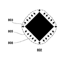
図65は本実施の形態の実施例16に係る液晶表示素子の基本構造を示す断面図である。図65に示すように、本実施例に係る液晶表示素子Jは、上側基板801と下側基板802とが対向配置され、その上側基板801と下側基板802との間に液晶層4が配置されている。上側基板801は、ガラス基板1の内面に透明電極2及び配向膜3が順次積層されて構成されている。また、下側基板802は、ガラス基板8の内面に透明電極7及び配向膜6が順次積層されるとともに、透明電極7上に立体障害803が立設されて構成されている。立体障害803は、先端が上側基板801に当接するように形成されており、その表面には配向膜が形成されていない。立体障害803は、本実施例では、菱形の横断面形状を有し、先端部が基部より細くなるよう傾斜した側面を有する柱状に形成されている。また、立体障害803は、本実施例では、フォトレジストで構成されている。また、立体障害803は後述するように撥水性を有しているので、製造工程において配向剤がはじかれ、そのため表面に配向膜を有しないものとなっている。
【0483】
次に、上記液晶表示素子Jの製作工程におけるラビング処理を詳しく説明する。
【0484】
図66は、図65の液晶表示素子の下側基板の配向処理を模式的に示す平面図である。
【0485】
図65、図66に示すように、立体障害803は、ラビング方向69に対し、その菱形の断面の対角線が略平行になるように下側基板802上に形成されている。そして、下側基板802に、符号69で示す方向にラビングを施した。すると、以下の知見が得られた。すなわち、下側基板802上の立体障害803の周辺部に、該立体障害803によるラビングのこすり下げ部分(以下、ラビングの影部分という。実施の形態18参照)804が形成される。そして、このラビングの影部分804において、立体障害803に近い部分に無ラビング領域805が形成され、それ以外の立体障害803から少し離れた部分に、通常のラビング方向69とは異なった方向にラビングされた異方向ラビング領域806が形成される。
【0486】
これは、本実施の形態では、ラビング布(図示せず)が立体障害803を乗り越えるので、基板802面にラビング布が接触しない領域が生じてそれが無ラビング領域805となり、また、ラビング布がはじかれることにより通常のラビング方向69とは異なった方向にラビングされる領域を生じてそれが異方向ラビング領域806となるためである。
【0487】
そして、上側基板801には、通常のラビング方向69にラビングを施した。
【0488】
このように配向処理された液晶表示素子Jでは、図66に示すように、異方向ラビング領域806において、液晶層4は、その配向処理方向に従ってラビング方向69に対し角度を持って配向し、無ラビング領域805において、液晶層4は立体障害803の撥水性又は親水性に応じた方向に配向する。そして、液晶表示素子Jのこれら以外の領域において、液晶層4はパラレル配向をする。つまり、異方向ラビング領域806内に、ラビング方向69に対し互いに逆方向に捩れたツイスト配向同士が相接するように形成され、それらツイスト配向がパラレル配向領域内に局所的に存在している。そのため、従来の構成の単純セルに比べて、ベンド転移する部分が格段に増加し、その結果、転移電圧が低くなるとともに、転移の確実性も格段に向上した。また、ラビング方向69に対し互いに逆方向に捩れたツイスト配向同士が相接する箇所を、ラビングにより効果的に形成することができた。
【0489】
ここで、ラビングの影部分804のラビング方向69における長さは、ラビング布の押し込み量Dp(図67参照)によって変化する。例えば、押し込み量Dp=0.3mmとしたとき、この領域804の上記長さはおよそ15〜30μm程度、Dp=0.7mmとしたとき、上記長さは10〜20μm程度であった。すなわち、ラビングする際に、押し込み量Dpを変化させることによりラビングの影部分804の上記長さを制御することができる。
【0490】
また、本実施例では、立体障害803の側面は、基部から先端に向かうに連れて内方に傾斜するように形成されているが、このように、立体障害803の側面を傾斜させると、立体障害803に撥水性が現れることが見出された。立体障害803の撥水性は、その側面の傾斜角が大きくなる程、強くなる。そして、立体障害803は、その側面が30度程度の傾斜角である場合から撥水性が現れはじめ、90度付近の傾斜角である場合まで撥水性を示した。この立体障害803は、先端部より基部を小さくしてもよい。そのようにしても撥水性が得られる。この立体障害803の撥水性の効果については、実施例19で詳しく説明する。
【0491】
なお、上記では液晶表示素子Jが基本的構成を有する場合を説明したが、本実施例では、立体障害及びその周辺部に電圧が印加されればよいので、アクティブマトリクスタイプその他の液晶表示素子にも、本実施例を上記と同様に適用することができる。
(実施例17)
図68は本実施の形態の実施例17に係る液晶表示素子の下側基板の配向処理を模式的に示す平面図である。
【0492】
図68を参照して、実施例16では、ラビング方向69と基板802のラビング用ローラに対する移動方向591とのなす角度、すなわちバイアス角度(実施の形態18参照)Θを略ゼロ度としたが、本実施例では、このバイアス角度Θを変化させ、立体障害803によるラビングの影部分804における配向処理を詳細に観察した。その結果、バイアス角度Θをある角度以上にすると、図示するように、異方向ラビング領域806における配向処理を、ラビング方向69から見て左右非対称(以下、単に左右非対称という)にすることが可能なことが見出された。具体的には、バイアス角度Θをゼロ度から増大させていくと、約15度ぐらいのバイアス角度Θから左右非対称性が顕著になり始め、30度から45度程度のバイアス角度Θで左右非対称性が非常に大きくなった。このように、異方向ラビング領域806における配向処理の左右非対称性を大きくすると、実施例20で詳しく述べるように、複数の立体障害を、各々のラビングの影部分804が互いに重なり合うように配設することにより、互いに逆方向に捩れた2つのツイスト配向を安定に形成することができる。
(実施例18)
図69は本実施の形態の実施例18に係る液晶表示素子の製造方法に用いるラビング用ローラの構成を示す模式図である。
【0493】
図69に示すように、本実施例においては、ラビング用ローラ517は、ラビング布のバフ毛(繊維)812が、ローラの回転軸方向に傾くよう、地布面811に植毛されている。このようなバフ毛812は、基板に対し角度を持って接触することになるため、立体障害による影部分の配向処理の左右非対称性が大きなる。
【0494】
よって、本実施例によれば、立体障害による影部分の配向処理の左右非対称性を大きくすることができる。
【0495】
また、その回転軸方向に傾くようにラビング布のバフ毛812が地布面811に植毛されたローラを用い、かつ基板の送り方向にバイアス角度を持たせるようにしてラビングすることにより、異方向ラビング領域の配向処理の左右非対称性を非常に大きくすることができた。
(実施例19)
図70は、本実施の形態の実施例19に係る液晶表示装置の下側基板の無ラビング領域における液晶の配向を模式的に示す平面図である。
【0496】
図70において、本実施例では、実施例16と異なり、下側基板802上に形成された立体障害803が撥水性の材料で構成されている。これ以外の点は実施例16と同様である。
【0497】
このような構成とすると、立体障害803周辺の無ラビング領域805内において、液晶をラビング方向69(図66参照)とは異なった方向808に配向させることができる。これは、立体障害803の撥水性によって液晶が立体障害803の側面に垂直に配向するためである。
【0498】
ここで、実施例16で述べた、立体障害803の側面を傾斜させることにより現れる撥水性によっても、本実施例における撥水性の効果と同様の効果が得られる。そして、本実施例においても、立体障害803は側面が実施例16と同様に傾斜している。このように、撥水性材料で構成された立体障害803の側面を、基部から先端に向かうに連れて内方に傾斜するよう形成すると、非常に強い撥水性を示すことが判明した。
【0499】
以上に述べたように、立体障害803に撥水性を持たせるとともにその周辺部に無ラビング領域805を形成すると、該無ラビング領域805において液晶が立体障害803の側面に垂直に配向し、それにより、平面視において放射状の配向が得られるため、互いに逆方向に捩れかつ相接する2つのツイスト配向を、効果的に、パラレル配向領域内に形成することができる。
(実施例20)
図71は、本実施の形態の実施例20に係る液晶表示素子の液晶の配向状態を模式的に示す平面図である。
【0500】
図71に示すように、本実施例では、実施例16と異なり、下側基板802上に、複数(図では2つ)の立体障害803が、各々のラビングの影部分804が互いに重なり合うように配設され、下側基板802にその送り方向519にバイアス角度Θを持たせるようにしてラビングが施され、かつ各々の立体障害803が撥水性の材料で構成されている。
【0501】
このような構成とすると、複数の立体障害803の異方向ラビング領域806が互いに重なり合い、かつバイアス角度Θを有するラビングにより各異方向ラビング領域806の配向に左右非対称性が付与されるため、立体障害803が単独に配設された場合に比べて、互いに逆方向に捩れた2つのツイスト配向を、さらに安定して形成することができた。ここで、立体障害803同士の距離が10〜30μmの場合に、互いに逆方向に捩れた2つのツイスト配向を安定して形成する効果が非常に高かった。さらに、本実施例では、各立体障害803が撥水性を有するので、それによって、さらに上記効果が増大する。このため、本実施例に係る液晶表示素子に転移電圧を印加したところ、従来の単純セルに比べて転移が発生する箇所が格段に増加し、液晶パネル全体が転移する電圧が格段に低くなり、かつ転移に要する時問が大きく短縮された。
(実施例21)
上記実施例16〜20では立体障害の断面形状を菱形としたが、本実施の形態の実施例21では、これを他の形状としたものである(図示せず)。例えば、立体障害の断面形状を円形や四角形とすることができる。立体障害の断面形状をこのような形状とすると、菱形形状とする場合より互いに逆方向に捩れた2つのツイスト配向を形成する効果は小さくなるが、立体障害の形成が容易になるというメリツトがある。
(実施例22)
上記実施例16及び実施例19では立体障害を撥水性としたが、本実施の形態の実施例22では、立体障害を親水性としたものである(図示せず)。その他の点は実施例16と同様である。このような構成とすると、立体障害の周辺の液晶が該立体障害の側面に平行に配向する。しかし、液晶の配向方向が変化するのは、立体障害の周辺の無ラビング領域内だけであるから、実施例16と同様に、異方向ラビング領域に、互いに逆方向に捩れた2つのツイスト配向を効果的に形成することができる。そして、本実施例によれば、親水性の材料は配向剤をはじきにくいので、立体障害の表面に配向膜が形成されるため、立体障害の周囲に形成されるパラレル配向領域の配向を余り乱さないというメリットがある。
(実施例23)
本実施の形態の実施例23は、立体障害を、基板間隔を保持する柱スペーサで構成したものである(図示せず)。立体障害を柱スペーサで構成すると、立体障害を別途設ける必要がないため、液晶表示素子を容易に作製することができる。また、柱スペーサの材料には、撥水性を強く示すもの、親水性を示すもの等様々なものがあるため、立体障害周辺部の液晶の配向を制御することが比較的容易となる。
(実施例24)
本実施の形態の実施例24は、液晶表示素子をアクティブマトリクスタイプのものとし、アレイ基板のアレイ構造の段差を立体障害として利用したものである。本実施例では、アレイ基板のアレイを形成する過程において、最大2μmの段差を形成することができた。この段差を利用してラビングを制御することにより、転移核となる異方向ラビング領域(実施例16参照)を形成することができた。本実施例では、柱スペーサを立体障害として利用する場合に比べると、転移核が発生する確率は低下したが、アレイ基板の作製にー般に採用しているアレイプロセスの変更だけで済むため、立体障害を容易に形成できるメリツトがある。
(実施例25)
実施例16、19では立体障害の表面を撥水性として垂直配向性に、実施例22では親水性として水平配向性にした。本実施の形態の実施例25は、立体障害としての柱スペーサの周辺に配向膜のテーパを形成することで配向方位を制御したものである。
【0502】
図72は本実施例に係る液晶表示素子の下側基板の液晶の配向を模式的に示す概念図であって、(a)は平面図、(b)は(a)のXXXXXXXIIb−XXXXXXXIIb矢視断面図である。
【0503】
図72(a)、(b)において、下側基板802上には複合柱スペーサを構成する3つ柱スペーサ803が形成されている。下側基板802の表面には配向膜824が形成されているが、各柱スペーサ803の表面には配向膜824が形成されていない。そして、配向膜824は、各柱スペーサ803の周辺で、柱スペーサから離れるに連れて膜厚が薄くなるようなテーパ824aが付されている。この下側基板802は、実施の形態2の図22と同様のラビング処理が施されている。
【0504】
このような構成とした結果、図72(a)に示すように、各柱スペーサ803の周辺821では液晶分子821aは該柱スペーサ803の側面に対して平行に配向する特性を示した。しかし、その外側の領域822では、液晶分子822aは、テーパの方向に従って配向し、さらにその外側の領域823では、液晶分子823aは、ラビング処理の方向に従って配向した。
【0505】
本実施例においては、このように配向膜824にテーパ824aを付すことにより、実施例19で示したような柱スペーサ803から放射状に延びる配向を実現することができた。これにより、液晶をスプレイ配向からベンド配向への転移させる際に、転移の核が形成された。
【0506】
上記テーパ構造は、配向膜を用いて形成するものに限るものではない。例えば、テーパが形成されるように樹脂をコーティングしてもよく、また、フォトレジストでテーパを形成してもよい。但し、配向膜を用いてテーパを形成することがもっとも簡便であった。
【0507】
テーパ構造の傾斜角は0.2度以上であればよく、マージンはかなり広い。
【0508】
なお、本実施例では、柱スペーサ803の周辺の傾斜構造は、直線的に傾斜しているが、曲線的であってもよい。
(実施例26)
本実施の形態の実施例26は、異配向方位領域を垂直配向領域としたものである。
【0509】
ベンド配向はパネルのセル厚方向における中央部で液晶が立っている構造であるため、片側の基板にでも液晶が立っている又はプレチルトが高い状態を形成すると転移が良好に発生した。
【0510】
本実施例では、ラビングを遮蔽する立体障害として柱スペーサを用い、この柱スペーサが形成された基板をラビングすることでラビング遮蔽領域を形成し、このラビング遮蔽領域を垂直配向となるようにした。
【0511】
すなわち、まず、柱スペーサの形成された基板に、配向膜として垂直配向性の強い膜を塗布し、硬化する。この基板にラビング処理を施すと、柱スペーサの背後の部分にラビングがなされないラビングの影領域が発生する。この現象は、図36(b)に示したものとほぼ同じである。但し、このラビングの影領域が垂直配向(基板面に垂直な配向)になる点が、図36(b)の場合と異なっている点であり、本実施例の特徴である。そして、液晶をスプレイ配向からベンド配向へ転移させる際に、この垂直配向領域を核に転移が発生した。
【0512】
この垂直配向領域は厳密に垂直である必要はない。この垂直配向領域は、プレチルトが20度以上の部分があればよく、望ましくはプレチルトが40度以上であるのがよい。プレチルトが40度以上であれば、電源を切断した後でもこの垂直配向領域はベンド配向を保持した。
【0513】
また、本垂直配向領域は両側の基板に形成しても、片側の基板に形成してもよい。
【0514】
【発明の効果】
本発明は以上に説明したような形態で実施され、速くかつ確実にスプレイ配向からベンド配向へ転移することができるという効果を奏する。そのため、その実用的価値は極めて大きい。
【図面の簡単な説明】
【図1】本発明の実施の形態1の実施例1に係るテストセルの構成を模式的に示す断面図である。
【図2】図1のテストセルの製造プロセスを示す断面図である。
【図3】図1のテストセルの製造プロセスを示す断面図である。
【図4】フォトマスクを示す平面図である。
【図5】図1の基板のラビング方向を示す図である。
【図6】本発明の実施の形態1の実施例2に係るテストセルの構成を模式的に示す断面図である。
【図7】フォトマスクを示す平面図である。
【図8】本発明の実施の形態1の実施例3に係るテストセルの構成を模式的に示す断面図である。
【図9】図8のテストセルの製造プロセスを示す断面図である。
【図10】マスクを示す平面図である。
【図11】本発明の実施の形態1の実施例4に係る液晶表示素子の構成を示す断面図である。
【図12】図11の液晶表示素子の各光学素子の配置方向を示す平面図である。
【図13】図11の液晶表示素子の正面における電圧−透過率特性を示すグラフである。
【図14】従来のOCBモード型液晶表示素子の構成を模式的に示す断面図である。
【図15】図1のテストセルの下側基板の突起の配置を模式的に示す平面図である。
【図16】図6のテストセルの下側基板の溝の配置を模式的に示す平面図である。
【図17】図8のテストセルの下側基板の配向処理状態を模式的に示す平面図である。
【図18】本発明の実施の形態1の実施例6に係る液晶表示素子の各光学素子の配置方向を示す平面図である。
【図19】本発明の実施の形態2に係る液晶表示素子の構成を示す平面図である。
【図20】図19のXX−XX矢視断面図である。
【図21】図19の複合柱スペーサの形態を示す平面図である。
【図22】図21の複合柱スペーサによって形成された配向処理状態を示す概念図である。
【図23】TFT基板上に形成された、複合柱スペーサを形成するための凹凸を模式的に示す断面図である。
【図24】ツイスト配向した液晶分子に隣接する液晶分子の挙動を模式的に示す図であり、(a)は電圧を印加しない場合の状態を示す断面図、(b)は電圧を印加しない場合の状態を示す平面図、(c)は所定の電圧を印加した場合の状態を示す断面図、(d)は電圧を印加した場合の状態を示す平面図である。
【図25】図19の液晶表示素子を転移させるために用いた転移電圧の波形を示す図である。
【図26】転移電圧に対する転移核発生率の変化を示す図である。
【図27】複合柱スペーサの変形例を示す平面図である。
【図28】複合柱スペーサを画素電極上に形成した変形例を模式的に示す平面図である。
【図29】複合柱スペーサをカラーフィルタ基板にカラーフィルタの段差を利用して形成した変形例を示す断面図である。
【図30】カラーフィルタ基板に、複合柱スペーサが当接しないようにするための凹部を形成した変形例を示す断面図である。
【図31】本発明の実施の形態4に係る液晶表示素子の構成を模式的に示す断面図である。
【図32】本発明の実施の形態6に係る液晶表示装置の構成を模式的に示すブロック図である。
【図33】本発明の実施の形態7に係る液晶表示装置の構成を模式的に示すブロック図である。
【図34】液晶表示素子における液晶の安定条件を示す概念図であり、(a)は基本的な液晶の安定条件を示す図、(b)はパラレル配向及びツイスト配向における液晶の安定条件を示す図である。
【図35】局所的にツイスト配向領域が形成された液晶表示素子におけるスプレイ−ベンド転移の過程を模式的に示す概念図であり、(a)は互いに逆方向の2つのツイスト配向領域が相接する場合を示す図、(b)は一方のツイスト角が90度である場合を示す図、(c)は一方のツイスト角が90度以上である場合を示す図、(d)は互いに同方向の2つのツイスト配向領域が相接する場合を示す図である。
【図36】本発明の実施の形態8に係る液晶表示素子の一方の基板の配向処理を模式的に示す平面図であって、(a)は1回目のラビングを施した後の状態を示す図、(b)は2回目のラビングを施した後の状態を示す図である。
【図37】本発明の実施の形態9に係る液晶表示素子の一方の基板の配向処理を模式的に示す平面図である。
【図38】本発明の実施の形態10に係る液晶表示素子の一方の基板の配向処理を模式的に示す平面図である。
【図39】本発明の実施の形態12に係る液晶表示素子のアクティブマトリクス基板の構成を模式的に示す平面図である。
【図40】本発明の実施の形態14に係る液晶表示素子の基板の配向処理の状態を模式的に示す平面図である。
【図41】本発明の実施の形態15に係る液晶表示素子の構成を模式的に示す断面図である。
【図42】本発明の実施の形態16に係る液晶表示素子の構成を模式的に示す図であって、(a)は断面図、(b)は平面図である。
【図43】図42の液晶表示素子に印加される駆動電圧の波形を示すグラフである。
【図44】本発明の実施の形態17に係る液晶表示素子の構成を模式的に示す図であって、(a)は断面図、(b)は平面図である。
【図45】図44の液晶表示素子に印加される駆動電圧の波形を示すグラフである。
【図46】本発明の実施の形態18に係る液晶表示素子の製造方法を示す模式図である。
【図47】本発明の実施の形態18に係る液晶表示素子の基板の配向処理の状態を示す平面図である。
【図48】本発明の実施の形態19に係る液晶表示素子の構成を模式的に示す平面図である。
【図49】図48のXXXXIX−XXXXIX矢視断面図である。
【図50】本発明の実施の形態20に係る液晶表示素子の構成を模式的に示す平面図である。
【図51】図50のXXXXXI−XXXXXI矢視断面図である。
【図52】本発明の実施の形態20の実施例7に係る液晶素子の下側基板の構成を示す斜視図である。
【図53】図50の液晶表示素子に印加される転移電圧の波形を示す図である。
【図54】液晶のスプレイ配向からベンド配向への転移を説明するための図であり、(a)はスプレイ配向を示す液晶表示素子の断面図、(b)はベンド配向を示す液晶表示素子の断面図である。
【図55】液晶の180度ツイスト配向を示す液晶表示素子の断面図である。
【図56】不完全囲繞体の外周面を傾斜させた構成例を示す下側基板の斜視図である。
【図57】本発明の実施の形態20の実施例8に係る液晶表示素子の下側基板の構成を示す斜視図である。
【図58】本発明の実施の形態20の実施例9に係る液晶表示素子の下側基板の構成を示す斜視図である。
【図59】本発明の実施の形態20の実施例10に係る液晶表示素子の下側基板の構成を示す図であり、(a)はビーズスペーサを一部が開放された環状に凝集させた構成例を示す平面図、(b)はビーズスペーサを互いの間に隙間を有してほぼ環状に並ぶように凝集させた構成例を示す平面図、(c)はビーズスペーサを環状に閉じるように凝集させた構成例を示す平面図である。
【図60】本発明の実施の形態20の実施例11に係る液晶表示素子の下側基板の構成を示す図であり、(a)は欠落部として貫通孔を有する不完全囲繞体を設けた構成例を示す斜視図、(b)は欠落部として上方に開放された切欠部を有する不完全囲繞体を設けた構成例を示す斜視図、(c)は欠落部として下方に開放された切欠部を有する不完全囲繞体を設けた構成例を示す斜視図である。
【図61】本発明の実施の形態23の実施例12に係る液晶表示素子の構成を模式的に示す画素単位の断面図である。
【図62】本発明の実施の形態23の実施例12に係る液晶表示素子の構成を模式的に示す画素単位の平面図である。
【図63】本発明の実施の形態23の実施例13に係る液晶表示素子の構成を模式的に示す画素単位の平面図である。
【図64】本発明の実施の形態23の実施例14に係る液晶表示素子の構成を模式的に示す画素単位の平面図である。
【図65】本発明の実施の形態24の実施例16に係る液晶表示素子の基本構造を示す断面図である
【図66】図65の液晶表示素子の下側基板の配向処理を模式的に示す平面図である。
【図67】ラビング布の押し込み量を説明するための模式図である。
【図68】本発明の実施の形態24の実施例17に係る液晶表示素子の下側基板の配向処理を模式的に示す平面図である。
【図69】本発明の実施の形態24の実施例18に係る液晶表示素子の製造方法に用いるラビング用ローラの構成を示す模式図である。
【図70】本発明の実施の形態24の実施例19に係る液晶表示装置の下側基板の無ラビング領域における液晶の配向を模式的に示す平面図である。
【図71】本発明の実施の形態24の実施例20に係る液晶表示素子の液晶の配向状態を模式的に示す平面図である。
【図72】本発明の実施の形態24の実施例に係る液晶表示素子の下側基板の液晶の配向を模式的に示す概念図であって、(a)は平面図、(b)は(a)のXXXXXXXIIb−XXXXXXXIIb矢視断面図である。
【符号の説明】
1,8 ガラス基板
2,7 透明電極
3,6 配向膜
4 液晶層
4’ ツイスト配向した液晶分子に隣接する液晶分子
4” ツイスト配向した液晶分子
4a スプレイ配向の液晶分子
4b ベンド配向の液晶分子
5 スペーサ
9 液晶セル
10 突起
11,14 負の一軸性フィルム位相板
12,15 主軸がハイブリッド配列した負の屈折率異方性を有する光学媒体よりなる位相差板
13,16 偏光板
17,18 位相補償板
19 正の一軸性フィルム位相板
20 フォトレジスト薄膜
21 フォトマスク
22 フォトマスク開口部
23 平行紫外線
30 溝
31 紫外線照射方向
32 紫外線の偏波面の延在方向
51 単位配向処理領域
61 ゲート線
62 ソース線
63 画素
64 画素電極
65 補助容量電極
66 スイッチ素子
67 ブラックマトリクス
68,77 絶縁層
69 ラビング方向
70 異方向配向処理領域
71 周囲の領域
72,86 凹部
73 カラーフィルタ等を含む層
74 平坦化層
75 配線層
76 カラーフィルタ
79 対向電極
80,81 矢印
84 セル厚方向
101 上側基板
102 下側基板
103 突起
104 溝
121 マスク
122 マスクの開口部
201 カラーフィルタ基板
202 TFT基板
203 複合柱スペーサ
203A,203B,203C 柱スペーサ
204 辺
205 ラビングが左右からぶつかる領域
301,308 液晶表示装置
302 コントローラ
303 基準電源回路
304 ゲートドライバ
305 ソースドライバ
306 転移電圧印加回路
307 映像信号
310 転移電圧印加用電極
401 パラレル配向領域
402 左回りツイスト領域
403 右回りツイスト領域
404 通常配列ツイスト
405 ベンド転移
406 ツイスト角が90度の領域
407 ツイスト角が90度以上の領域
408 左回りツイスト領域
501 基板
502 柱スペーサ
503 影領域
504 キズ
505 右回りツイストの領域
506 左回りツイストの領域
507 基準方向
508 ツイスト配向領域
509 ツイスト配向領域の配向方向
510 立体障害
511 柱スペーサの周辺に位置する液晶分子の配向方向
512 ダミーパターン
513 横電界
514 画素電圧
515 対向電圧
516 ゲート電圧
517 ラビング用ローラ
518 ローラの回転方向
519 ラビングの影部分
518a,519c 右方向にラビングされる領域
518b,519d 左方向にラビングされる領域
520 接触箇所
540 パラレル配向領域
541 全体的なパラレル配向領域
542 表示域
543 柱スペーサが形成される箇所
544 ジグザグ形状
544a,544b 傾斜直線
545 対向電圧及びゲート電圧がローレベルである期間
591 基板の移動方向
601 不完全囲繞体
601a 外周面
602 欠落部
603 過渡的配向保存領域
611a,611b,611c,611d 板状体
612 ビーズスペーサ
701 カラーフィルタ基板
702 アレイ基板
703 位相補償板
704 配向処理方向
711 横電界によるツイスト配向
712 転移核
801 上側基板
802 下側基板
803 立体障害
804 ラビングの影部分
805 無ラビング領域
806 異方向ラビング領域
811 地布面
812 バフ毛
821 柱スペーサの周辺
821a,822a,8223a 液晶分子
822 柱スペーサの周辺の外側の領域
823 柱スペーサの周辺のさらなる外側の領域
824 配向膜
A〜C テストセル(液晶表示素子)
D〜J 液晶表示素子
Dp 押し込み量
P ジグザグ形状のピッチ
θ 照射角度
Θ バイアス角度[0001]
BACKGROUND OF THE INVENTION
The present invention relates to a liquid crystal display element having a high response speed and a wide viewing angle display, a substrate for a liquid crystal display element, a liquid crystal display device, a method for manufacturing the liquid crystal display element, and a method for driving the liquid crystal display element. The present invention relates to an easily self-compensated birefringence mode cell type spray-bend transition.
[0002]
[Prior art]
As multimedia technology advances, the proportion of image information is increasing. Recently, with the development of liquid crystal technology, a liquid crystal display with a high contrast and a wide viewing angle has been developed and put into practical use, and has reached a level comparable to that of a CRT display.
[0003]
However, the current liquid crystal display has a problem that the image is blurred due to an afterimage in moving image display because the response speed is slow, and this is inferior to the CRT display.
[0004]
Many attempts have been made to increase the response speed of liquid crystal displays. Various liquid crystal display systems with high-speed response are summarized by Wu et al. (CS Wu and ST Wu, SPIE, 1665, 250 (1992)), but a system and method that can expect response characteristics necessary for moving image display. Is limited.
[0005]
In other words, in the current NTSC system, the liquid crystal needs to follow within one frame (16.7 msec). However, the current liquid crystal display displays sufficiently fast response between black and white, but performs multi-gradation display. In this case, the response between gradations becomes a slow response of 100 msec or more. In particular, the response between gradations in a region where the driving voltage is low is extremely slow.
[0006]
At present, OCB mode liquid crystal display elements, ferroelectric liquid crystal display elements, and antiferroelectric liquid crystal display elements have the potential as high-speed response liquid crystal displays suitable for moving image display.
[0007]
However, ferroelectric liquid crystal display elements having a layer structure and anti-ferroelectric liquid crystal display elements have problems in practical meaning such as low impact resistance, narrow operating temperature range, and large temperature dependence of characteristics. In reality, OCB mode liquid crystal display elements using nematic liquid crystals are actually promising as liquid crystal display elements suitable for moving image display.
[0008]
This OCB mode liquid crystal display element is a display system whose high speed was shown by JPBos in 1983, and then combined with a film phase difference plate to achieve both a wide viewing angle and high speed response. The research and development was activated.
[0009]
As shown in FIG. 14, the liquid crystal display element in this mode is disposed between a
[0010]
In the liquid crystal cell having such a structure, bend alignment including twist alignment or twist alignment is induced in the center of the cell by applying a voltage, and
[0011]
The OCB mode liquid crystal display element is normally operated at a voltage that maintains the bend alignment of the liquid crystal inside the liquid crystal panel. However, when the voltage is lower than a certain voltage, the splay alignment state is more stable than the bend alignment state. Therefore, transition to splay alignment occurs. This transition is irreversible, and the pixel in which the splay alignment once occurs is then left as a display defect (bright spot) on the liquid crystal display element, preventing its normal display operation.
[0012]
[Problems to be solved by the invention]
By the way, in the OCB mode, an initialization process for transferring from the initial
[0013]
However, when a voltage of about several volts is applied, the initialization process requires time in minutes, which is one of the problems of the OCB mode. Therefore, there is a demand for a liquid crystal display element having a high transition speed in which bend alignment is easily formed by applying a voltage of about several volts.
[0014]
On the other hand, JP-A-11-7018 discloses a technique for speeding up the transition from splay alignment to bend alignment (hereinafter referred to as spray-bend transition) in the OCB type liquid crystal display mode. As the technology, an example in which a chiral agent is added to the liquid crystal, an example in which a twist of 180 degrees is uniformly formed on the entire surface of the liquid crystal panel, and an example in which a twist of 10 degrees is uniformly formed on the entire surface of the liquid crystal panel are shown. However, these techniques are not sufficient to speed up the spray-bend transition. And this splay-bend transition is not performed reliably, and when the area | region of the splay alignment remains locally, there existed a problem that there appeared as a luminescent point and it looked like a point defect.
[0015]
The present invention has been made in order to solve such problems, and a liquid crystal display element having a fast and reliable transition from a splay alignment to a bend alignment.ChildIt is an object of the present invention to provide a method for driving a liquid crystal display element.
[0016]
[Means for Solving the Problems]
In order to solve the above problems, the present inventors have observed the behavior of the spray-bend transition. As a result, it was found that nuclei of bend orientation were generated from a specific location and grew. Furthermore, as a result of intensive investigations, the present inventor has found that a bend transition occurs with a twist alignment locally formed as a nucleus.
[0018]
The liquid crystal display element according to the present invention includes a pair of substrates.And the liquid placed between these substratesWith crystal layerOCB mode liquidA crystal display element, and the pair of substrates are both subjected to a substantially parallel orientation process.The twist alignment of the orientation different from the orientation orientation of the liquid crystal molecules by the orientation treatment is localized.PlaceDifferent in formingOrientation directionAlso have means to form a zoneBecauseThe
[0214]
The driving method of the liquid crystal display element according to the present invention is as follows.A method of driving the liquid crystal display element,Source lines, gate lines, and pixel electrodes are formed on one of the substrates, and a counter electrode is formed on the other substrate.Before the period of forming the different orientation direction region,To gate lineSpecialApplying a constant sign gate voltage, the source lineThe aboveVoltage opposite to the gate voltage is applied to the counter electrode.Is the aboveA period for applying a voltage having the same sign as the gate voltage exists.The
[0216]
Also, a method for driving a liquid crystal display element according to the present inventionIs a method of driving the liquid crystal display element,Source lines, gate lines, and pixel electrodes are formed on one of the substrates, and a counter electrode is formed on the other substrate.In the period of forming the different orientation direction region,Adjacent source lineCompanionDifferent voltagesApplyIt is whatThe
[0255]
DETAILED DESCRIPTION OF THE INVENTION
Hereinafter, embodiments of the present invention will be described with reference to the drawings.
[Test cell]
In the following Examples 1 to 3, a liquid crystal display element as a test cell was produced, and the spray-bend transition time was evaluated for the produced test cell. Since the phase compensation plate is not required for evaluating the spray-bend transition time, the phase compensation plate is omitted in the test cells of Examples 1 to 3.
Example 1
1 is a cross-sectional view schematically showing the configuration of a test cell according to Example 1 of the present embodiment, and FIG. 15 is a plan view schematically showing the arrangement of protrusions on the lower substrate of the test cell of FIG. . FIG. 5 is a diagram showing the rubbing direction of the substrate of FIG.
[0256]
As shown in FIGS. 1 and 15, the test cell A according to the present embodiment includes a pair of substrates, that is, an
[0257]
The
[0258]
As shown in FIG. 5, the
[0259]
Although only two
[0260]
Next, a method for manufacturing the test cell configured as described above will be described with reference to FIGS. 2 and 3 are sectional views showing a manufacturing process of the test cell of FIG. 1, and FIG. 4 is a plan view showing a photomask.
[0261]
First, as shown in FIG. 2A, a PC type resist material manufactured by JSR Corporation is applied on a
[0262]
Next, ITO (indium tin oxide) is formed to a thickness of 2000 angstroms on the
[0263]
Further, the
[0264]
Next, the
[0265]
Next, the
[0266]
Next, liquid crystal MJ96435 (refractive index anisotropy Δn = 0.138) is injected into the
[0267]
Next, the evaluation of the spray-bend transition time of the test cell A produced by the above manufacturing method will be described.
[0268]
First, two polarizing plates are attached to the upper and lower surfaces of the test cell A so that each polarization axis forms an angle of 45 degrees with the rubbing treatment direction of the alignment film and the polarization axis directions are orthogonal to each other. After that, when a rectangular wave voltage of 7 V was applied between the
[0269]
That is, in the test cell A, in the region near the
[0270]
As a comparative example, a test cell R having the same configuration except that the
[0271]
In this embodiment, the
(Example 2)
6 is a cross-sectional view schematically showing the configuration of a test cell according to Example 2 of the present embodiment, and FIG. 16 is a plan view schematically showing the arrangement of grooves in the lower substrate of the test cell of FIG. .
[0272]
As shown in FIGS. 6 and 16, the test cell B according to the present embodiment is different from the first embodiment in that a
[0273]
Next, a method for manufacturing the test cell B configured as described above will be described with reference to FIGS. FIG. 7 is a plan view showing a photomask.
[0274]
First, a photoresist
[0275]
Thereafter, the
[0276]
Then, the
[0277]
Thereafter, in the same manner as in Example 1, a
[0278]
Next, evaluation of the spray-bend transition time of the test cell B produced by the above manufacturing method will be described.
[0279]
First, two polarizing plates are attached to the upper and lower surfaces of the test cell B so that each polarization axis forms an angle of 45 degrees with the rubbing treatment direction of the alignment film and the polarization axis directions are orthogonal to each other. Thereafter, when a 7 V rectangular wave voltage was applied between the
[0280]
In the test cell B, in the region where the
[0281]
In this embodiment, the
[0282]
In this embodiment, the inclination angle of the
(Example 3)
FIG. 8 is a cross-sectional view schematically showing the configuration of the test cell according to Example 3 of the present embodiment, and FIG. 17 is a plan view schematically showing the alignment processing state of the lower substrate of the test cell of FIG. .
[0283]
As shown in FIGS. 8 and 17, in the test cell C according to the present embodiment, unlike the first embodiment, the
[0284]
Next, a method for manufacturing the test cell C configured as described above will be described with reference to FIGS. FIG. 9 is a sectional view showing a manufacturing process of the test cell of FIG. 8, and FIG. 10 is a plan view showing a mask.
[0285]
First, as in Example 1, the
[0286]
Next, the
[0287]
Next, the
[0288]
Subsequently, the processing A and the processing B are performed by changing the irradiation angle θ of the polarized ultraviolet rays to 45 degrees and the irradiation time to 3 minutes (processing A ′ and processing B ′). Thereby, the photo-alignment processing of the
[0289]
Next, the
[0290]
Next, in the same manner as in Example 1, a
[0291]
Next, evaluation of the spray-bend transition time of the test cell C produced by the above manufacturing method will be described.
[0292]
First, on the upper surface and the lower surface of the test cell C, the respective polarization axes form an angle of 45 degrees with the average orientation direction of the liquid crystal molecules of the two types of unit alignment regions whose orientation directions are different from each other by 90 degrees, and the polarization of each other. Two polarizing plates were pasted so that the axial directions were orthogonal, and then a 7 V rectangular wave voltage was applied between the
[0293]
This is because a transition nucleus is generated from a region on each unit
[0294]
In this embodiment, the unit orientation processing region is not particularly associated with the pixel, but it may be associated with the pixel.
[Liquid crystal display element]
Example 4
FIG. 11 is a cross-sectional view showing the configuration of the liquid crystal display element according to Example 4 of the present embodiment, and FIG. 12 is a plan view showing the arrangement direction of each optical element of the liquid crystal display element of FIG. In FIG. 11, the description of the protrusion 103 (see FIG. 1) of the
[0295]
In this embodiment, the retardation values of the
[0296]
Next, evaluation of the performance of the liquid crystal display element D configured as described above will be described.
[0297]
FIG. 13 is a graph showing voltage-transmittance characteristics in front of the liquid crystal display element D at 25 ° C. This voltage-transmittance characteristic is obtained by applying a 10 V rectangular wave voltage to the liquid crystal display element D for 10 seconds to confirm that the liquid crystal display element D has transitioned to bend alignment, and then measuring the transmittance while decreasing the voltage. It was. In the liquid crystal display element D, since the transition from the bend alignment to the splay alignment occurs at 2.1 V, it is necessary to effectively display at a voltage of 2.2 V or more. On the other hand, in this voltage-transmittance characteristic, the transmittance is minimum in the vicinity of 7.2V. Therefore, the white level voltage was 2.2 V and the black level voltage was 7.2 V, and the viewing angle dependence of the contrast ratio at this time was measured. As a result, a contrast ratio of 10: 1 or more is achieved in a range of 126 degrees up and down and 160 degrees on the left and right, and it is sufficient even if a portion where the direction of the liquid crystal director is different from the surrounding is provided on the substrate alignment film surface. It was confirmed that a wide viewing angle characteristic was maintained. Further, in visual observation, neither orientation failure nor display quality failure was observed.
[0298]
The response time when the applied voltage was changed from 3 V to 5 V was measured. The rise time was 5 milliseconds. The response time when the applied voltage was changed from 5 V to 3 V was measured. The fall time was 6 milliseconds.
(Example 5)
A liquid crystal display element (not shown) according to Example 5 of the present embodiment uses the test cell B according to Example 2 instead of the test cell A in the liquid crystal display element D according to Example 4 ( Not shown). Even with such a configuration, the same effect as in the fourth embodiment can be obtained.
(Example 6)
A liquid crystal display element (not shown) according to Example 6 of the present embodiment uses the test cell C according to Example 3 instead of the test cell A in the liquid crystal display element D according to Example 4 ( Not shown). However, the optical elements are arranged in the direction shown in FIG.
[0299]
Even with such a configuration, the same effect as in the fourth embodiment can be obtained.
[0300]
As is clear from the above, in the liquid crystal display element according to the first embodiment, high-speed splay-bend alignment transition can be achieved without sacrificing the wide viewing angle characteristics and response characteristics of the conventional OCB mode. Yes, its practical value is enormous.
The second embodiment of the present invention exemplifies a preferable form of a protrusion (steric hindrance) for controlling the alignment process by rubbing.
[0301]
19 is a plan view showing the configuration of the liquid crystal display element according to
[0302]
As shown in FIGS. 19 and 20, the liquid crystal display element E of the present embodiment is an active matrix type OCB mode liquid crystal display element, and faces the TFT substrate (array substrate) 202 and the
[0303]
The
[0304]
The
[0305]
Next, the
[0306]
In the liquid crystal display element E, the
[0307]
As an example of the form of the column spacer of the present invention, in the present embodiment, as shown in FIG. 21,
[0308]
In the
[0309]
When the
[0310]
In FIG. 22, an arrow with a
[0311]
Next, preferable conditions for the form of the
[0312]
Further, the interval between the two
[0313]
Moreover, it is preferable that the length of the diagonal line with the shorter rhombic cross section of each column spacer 203A, 203B, 203C is 5 μm or more. This is because if the length of the diagonal line is short, the column spacer is likely to fall. When the column spacer has a cross section of an arbitrary shape, the minimum diameter is preferably 5 μm or more. Here, in this specification, the diameter of the column spacer (steric hindrance) refers to the distance between two points on the outer periphery of the cross section across the center point of the cross section of the column spacer.
[0314]
Further, in order to generate nuclei of the spray-bend transition, it is at least necessary that twist alignment is generated in the
[0315]
Further, the vicinity of the protrusions formed on the substrate including the
[0316]
Further, when the protrusion has a height that is more than half of the thickness of the liquid crystal layer 4 (referred to as a cell thickness in the present specification), it easily becomes a transition nucleus. In order to make the protrusions become transition nuclei more reliably, it is desirable that the protrusions have a height equal to the cell thickness or a difference of 1 μm or less from the cell thickness.
[0317]
In this embodiment, as can be seen from FIG. 21, the twist angle of the twist alignment region is about 60 degrees. The twist alignment region easily becomes a transition nucleus when the twist angle is 45 ° or more, and is more effective when the twist angle is 60 ° or more. Furthermore, if there is a twist alignment region having a twist angle of 90 °, the region is transferred even at a voltage as low as about 5V. This is because a clockwise twist and a counterclockwise twist can coexist in this area as will be described in detail in the eighth embodiment. Therefore, the twist angle of the twist alignment region is preferably 45 degrees or more and 90 degrees or less, and more preferably 60 degrees or more and 90 degrees or less. In this embodiment, the twist alignment region does not need to be uniform. When the orientation direction of the liquid crystal has a distribution and gradually changes, there is a tendency that the liquid crystal is easily transferred.
[0318]
In the present embodiment, the side surfaces of the
[0319]
In this embodiment, a
[0320]
In this embodiment, one
[0321]
In this embodiment, the height of the portion where the
[0322]
In addition, an insulating
[0323]
Next, the operation of the liquid crystal display element E configured as described above will be described with reference to FIGS.
[0324]
19 to 22, when a transition voltage is applied to the liquid crystal display element E, transition nuclei are formed in the twist alignment region of the
[0325]
Here, the reason why the spray-bend transition is easily performed will be theoretically considered. In order to transition from the splay alignment to the bend alignment, an energy barrier exists, and therefore, a transition voltage for exceeding the energy barrier is required. In addition, a transition nucleus is required for the spray-bend transition.
[0326]
Consider a liquid crystal molecule 4 'adjacent to a twist-aligned
[0327]
Here, the voltage at which the
[0328]
Next, the above effect will be specifically described. FIG. 25 is a diagram showing a waveform of a transition voltage used for transition of the liquid crystal display element E. When a one-pulse square wave voltage having a voltage value of 15 V and a pulse width of 0.5 seconds shown in FIG. 25 was applied to the liquid crystal display element E, the liquid crystal display element E transitioned from the splay alignment to the bend alignment. In the study of the present inventors, a transition voltage of about 25V has been conventionally required. Therefore, it can be seen that the liquid crystal display element E can be transferred at an extremely low voltage and in an extremely short time as compared with the conventional case. Further, the voltage of the waveform in FIG. 25 may be applied multiple times. Moreover, when the voltage of this waveform was used, the transition could be reliably performed even at a temperature of −10 ° C.
[0329]
FIG. 26 is a diagram showing a change in transition nucleus generation rate with respect to the transition voltage. FIG. 26 shows changes in the generation rate of transition nuclei in the pixel when the transition voltage is changed at temperatures of −10 ° C., 0 ° C., 25 ° C. (room temperature), and 50 ° C. According to FIG. 26, regardless of the temperature, the transition voltage is about 10 V or more and the transition nucleus generation rate is 100%. Therefore, it can be seen that when the transition voltage is about 10 V, the liquid crystal display element E can reliably perform the transition for each pixel and prevent the occurrence of point defects in units of pixels. Further, since transition nuclei are generated at 4V, it can be understood that the transition can be performed at a transition voltage of 4V as long as time is required.
[0330]
Next, a modification of the liquid crystal display device according to this embodiment will be described.
[0331]
In the above configuration, the composite pillar spacer has the form shown in FIG. 21, but the form of the composite pillar spacer is not limited to this, and may be as shown in FIG. FIG. 27 is a plan view showing a modification of the composite pillar spacer. 27A and 27B includes a single column spacer, and the column spacer has a cross-sectional shape having a side perpendicular to the rubbing
[0332]
In the above configuration, the
[0333]
Further, in the above configuration, the
[0334]
Further, in the above configuration, the portion of the
[0335]
In the above configuration, the liquid crystal display element E is formed of an active matrix type. However, the essence of the present embodiment is to provide a composite column spacer for rubbing control on the substrate. Any type. Therefore, the present invention can be similarly applied to other types such as a passive matrix type.
In
[0336]
In the second embodiment, the
The fourth embodiment of the present invention differs from the second embodiment in that the
In the fifth embodiment of the present invention, a region that is locally aligned in a direction different from the alignment processing direction of the surrounding region is formed by photo-alignment. Since the essence of the present invention is to form a twist alignment region, the alignment treatment method is basically not limited. Therefore, the effect of the present invention can be obtained even if the twist alignment region is formed by photo-alignment. For example, an effect similar to that of the second embodiment can be obtained by performing an alignment process as shown in FIG. 22 by optical alignment. However, the substrate on which the photo-alignment treatment is performed needs to form the alignment film with the photo-alignment film. Other points may be the same as in the second embodiment.
In the sixth embodiment of the present invention, a liquid crystal display device is configured using the liquid crystal display element according to the second embodiment.
[0337]
As shown in FIG. 32, the liquid
[0338]
Next, the transition operation of the liquid
[0339]
In the above configuration, the liquid crystal display element is configured to transition at 4 V. However, since the driving voltage of the liquid crystal display element in the liquid crystal display device is about 10 V at the maximum, the liquid crystal display element transitions at 10 V or less. Anything is acceptable.
In the seventh embodiment of the present invention, the liquid crystal display device includes a power supply dedicated for transfer. That is, as shown in FIG. 33, unlike the sixth embodiment, the liquid
[0340]
In the liquid
In the second embodiment, the spray-bend transition can be ensured by locally controlling the rubbing direction. In the eighth embodiment of the present invention, this transition process is examined in more detail, and as a result, generation of transition nuclei is ensured.
[0341]
FIG. 34 is a conceptual diagram showing the stability conditions of the liquid crystal in the liquid crystal display element, (a) is a diagram showing the basic liquid crystal stability conditions, and (b) is a diagram showing the stability conditions of the liquid crystal in parallel alignment and twist alignment. It is. FIG. 35 is a conceptual diagram schematically showing the process of spray-bend transition in a liquid crystal display element in which a twist alignment region is locally formed. FIG. 35A shows two twist alignment regions in opposite directions. A diagram showing a case of contact, (b) a diagram showing a case where one twist angle is 90 degrees, (c) a diagram showing a case where one twist angle is 90 degrees or more, and (d) showing each other It is a figure which shows the case where two twist orientation area | regions of the same direction contact | connect.
[0342]
As shown in FIG. 34 (a), the liquid crystal basically prefers a normal alignment state in which the tilt angle with respect to the substrate does not change, and prefers a state with little twist deformation.
[0343]
However, a state where these two conditions are contradictory is represented by a parallel alignment state. Further, even in the alignment with a twist angle of 90 degrees or less, the stability condition of the liquid crystal is basically the same as in the parallel alignment state. As shown in FIG. 34 (b), in the state where no voltage is applied, the splay alignment with a twist angle of 0 degrees is stable in terms of energy in the parallel alignment state. However, when a voltage of about 2 V or more is applied, the normal arrangement with a twist angle of 180 degrees is stable in terms of energy. It was confirmed that when the 180-degree twist was stabilized by the application of voltage, the transition to the bend alignment was made immediately from this state. Therefore, it is necessary to transiently form this 180 degree twist state. However, even if the 180-degree twist state becomes energetically stable by voltage application, it does not easily change to 180-degree twist in practice. This is because the structural change is large and a nucleus for this transition is required. The point of the present invention is how to reliably form this transition nucleus. It should be noted that even in a spray twist orientation with a twist angle of 90 degrees or less, the twist angle that becomes energetically stable when a voltage of about 2 V or more is applied is 180 degrees −θ (θ is the twist angle). This is similar to the parallel orientation.
[0344]
FIG. 35 (a) is a diagram showing a case where composite column spacers are formed as shown in the second embodiment. At this time, metastasis occurs through the following process.
[0345]
As shown in FIG. 35 (a), a
[0346]
Furthermore, since the outer
[0347]
As described above, it has been found that when the
[0348]
Furthermore, the twist angle was increased and examined. As shown in FIG. 35 (b), when the twist angle of one
[0349]
As shown in FIG. 35 (c), when the twist angle of one
[0350]
Next, a method for forming the twist alignment region as described above will be described. As shown in FIG. 35A, locally forming the clockwise twist region and the counterclockwise twist region adjacent to each other in the parallel alignment region is formed on the substrate as described in the second embodiment. This can be realized by forming a composite column spacer and performing rubbing.
[0351]
On the other hand, as shown in FIGS. 35 (b) and 35 (c), the formation of the twist alignment region having a twist angle of 90 degrees or more in the parallel alignment region is as described in the previous embodiments. It was impossible to realize with one alignment process. Therefore, the present inventor has realized this by performing rubbing twice on the substrate on which the column spacer is formed. This will be specifically described with reference to FIG.
[0352]
FIG. 36 is a plan view schematically showing the alignment treatment of one substrate of the liquid crystal display element according to the present embodiment, and FIG. 36 (a) shows a state after the first rubbing. ) Is a diagram showing a state after the second rubbing. As shown in FIG. 36 (a), the
[0353]
In order to form such a twist alignment region having a twist angle of 90 degrees or more, it is also effective to add some chiral agent to the liquid crystal. That is, it is generally difficult to form a twist alignment region having a twist angle of 90 degrees or more unless a chiral agent is added. This is the same even when a plurality of rubbing processes are performed. However, as described above, when a twist alignment region having a twist angle of 90 degrees or more is formed, it becomes a transition nucleus. Therefore, when a chiral agent is added, the orientation state in a specific rotational direction becomes stable. For example, when a clockwise chiral agent is added, the clockwise twist orientation region becomes stable, and even if the twist angle is 90 degrees or more, it can exist stably. Thus, the chiral agent was effective in forming a twist alignment region having a twist angle of 90 degrees or more.
[0354]
When the liquid crystal display element as described in the second embodiment is formed using the substrate subjected to the alignment treatment by the above method, a transition nucleus from the splay alignment to the bend alignment is surely generated. Can be obtained.
In the ninth embodiment of the present invention, different alignment orientation regions which are in contact with each other are formed by forming scratches on the alignment film.
[0355]
FIG. 37 is a plan view schematically showing the alignment treatment of one substrate of the liquid crystal display element according to the present embodiment.
[0356]
In FIG. 37, an alignment film (not shown) is formed on the surface layer portion of one
[0357]
With such a configuration, by performing a parallel alignment process on the other substrate, the liquid crystal molecules positioned on the
[0358]
Here, the scratch refers to a state in which the alignment film is partially missing. In order to form this scratch, it may be removed by etching using a photoresist. Alternatively, a liquid that dissolves in a specific solvent and an insoluble liquid may be mixed, emulsified and cured, and then one of them may be removed with the solvent.
In the tenth embodiment of the present invention, a twist alignment region having a twist angle of 90 degrees or more is formed by performing a local alignment process by photo-alignment.
[0359]
FIG. 38 is a plan view schematically showing the alignment treatment of one substrate of the liquid crystal display element according to the present embodiment.
[0360]
In FIG. 38, one
[0361]
This alignment treatment was performed as follows. First, an alignment film having a photosensitive group is formed on the surface layer portion of the
[0362]
With such a configuration, by performing parallel alignment treatment on the other substrate, the liquid crystal display element has a twist alignment region with a twist angle of 90 degrees or more. Therefore, as described in
The eleventh embodiment of the present invention shows a desirable density of transition nuclei.
[0363]
That is, the essence of the present invention is to form a transition nucleus. However, if there are irregularities on the substrate, the transition often stops at these irregularities. Therefore, it is important to form more transition nuclei in order to ensure the transition. As an imagination, it is desirable to form a transition nucleus in each pixel.
[0364]
Here, in consideration of practicality, it is desirable that this transition nucleus (more precisely, the steric hindrance for forming a different orientation direction region serving as a transition nucleus) also serves as a column spacer. When transition nuclei composed of column spacers are formed, there is a problem that the column spacers become excessive. This problem was solved by reducing the number of column spacers that contact the counterpart substrate using the unevenness provided on the substrate. This has been described in the second embodiment. Therefore, according to this method, transition nuclei can be formed in each pixel without causing any particular problem, thereby realizing an ideal density of transition nuclei.
[0365]
However, if the number of transition nuclei is small, the manufacturing cost can be reduced, and this is not exceeded. As a result of further studies, the following was found regarding the density of transition nuclei.
[0366]
That is, first, in order to obtain the effect of the present invention, it is not necessary to form transition nuclei in each pixel, but it is desirable to form transition nuclei at a density of 1 or more in 100 pixels.
[0367]
Second, if transition nuclei are formed at a density of 1 or more in 10 pixels, the entire panel can be transferred almost certainly.
[0368]
Thirdly, in the embodiments so far including this embodiment, the transition nuclei are periodically formed on the substrate. However, it is not always necessary to periodically form the transition nuclei. Rather, when the transition nuclei are periodically formed on the substrate, when the pattern for forming transition nuclei is shifted when a panel is formed using a photolithographic method, the image is moire during the display operation of the completed liquid crystal display element. The problem arises that it may look like However, this problem could be solved by randomly forming transition nuclei on the substrate and making the transition nucleation pattern random.
[0369]
The liquid crystal display element according to the present embodiment is configured to satisfy the first to third conditions.
As described in the eleventh embodiment, the growth of transition between pixels may stop due to unevenness on the substrate, but the twelfth embodiment of the present invention does not inhibit or promote the growth of transition between pixels. For this purpose, transition nuclei are formed on the source line.
[0370]
FIG. 39 is a plan view schematically showing the configuration of the active matrix substrate of the liquid crystal display element according to the present embodiment.
[0371]
In FIG. 39, in the present embodiment, a plurality (three in this case) of three-
[0372]
In the liquid crystal display device configured as described above, a defect, particularly a defect between two types of splay alignment states (a region having a splay alignment center in the vicinity of one substrate and a splay alignment center in the vicinity of the other substrate) is caused by
[0373]
Note that, as described in detail in
In the thirteenth embodiment of the present invention, the steric hindrance for controlling the rubbing is formed by using the step of the array structure on the array substrate without using the column spacer.
[0374]
In the present embodiment, a step of 2 μm at maximum could be formed in the process of forming the array substrate array. Then, when the alignment treatment was performed on the array substrate, transition nuclei (different orientation direction regions) could be formed by controlling rubbing using the step of 2 μm at the maximum.
[0375]
In the liquid crystal display element using the array substrate thus created, the probability of transition from the splay alignment to the bend alignment is lower than when the column spacer is used. However, in order to obtain the liquid crystal display element having the transition nucleus of the present invention, it is only necessary to change the array process generally used for manufacturing the array substrate. Therefore, there is an advantage that the transition nucleus can be easily formed. Further, the effect of ensuring bend transition can be further enhanced by combining the alignment treatment method according to the present embodiment with the alignment treatment method described in
In the fourteenth embodiment of the present invention, a column spacer (steric hindrance) is made water-repellent in order to form a different orientation direction region.
[0376]
FIG. 40 is a plan view schematically showing a state of alignment processing of the substrate of the liquid crystal display element according to the present embodiment.
[0377]
In FIG. 40, a
[0378]
When forming the
[0379]
In addition, in the present embodiment, what is important is that a region that is not rubbed or very weakly rubbed is formed on the substrate, and that other liquid crystal molecules positioned in the region are aligned in a predetermined direction. Having an orientation means. In this embodiment, the other orientation means is the water repellency of the column spacer.
In the fifteenth embodiment of the present invention, column spacers formed in the periphery of the display area of the substrate also function as spacers that maintain the substrate spacing.
[0380]
In the present invention, a transition nucleus is generated to ensure bend transition. In the second embodiment, a column spacer is used as the transition nucleus, and the column spacer is formed on the auxiliary capacitance electrode. By the way, in the active matrix type liquid crystal display element, the portion where the auxiliary capacitance of the TFT substrate is formed is about 1 μm higher than the pixel portion on the TFT substrate side by the array structure. In addition, since the black matrix is also formed in the portion where the auxiliary capacitor of the force Luller filter substrate is formed, this is also higher than the pixel portion of the color filter substrate. For this reason, the column spacer formed in the portion where the auxiliary capacitance is formed functions as a spacer for maintaining the distance between the substrates because it contacts both substrates. However, the pillar spacer formed in the area outside the display area of the panel does not function as a spacer for maintaining the gap between the substrates because the step of the active matrix is not formed in the area. There was a problem that the cell thickness was reduced on the outside.
[0381]
As a solution to this problem, in order to compensate for the step corresponding to the step of the active matrix, a spacer made of glass fiber of a predetermined size is mixed inside the sealing resin layer formed outside the display area of the TFT substrate. Is also possible. However, if this is done, the signal wiring may be damaged by the spacer.
[0382]
Therefore, in the present embodiment, the following configuration is adopted to solve this problem.
[0383]
FIG. 41 is a cross-sectional view schematically showing the configuration of the liquid crystal display element according to the present embodiment. 41, the same reference numerals as those in FIG. 20 denote the same or corresponding parts. Also, in FIG. 41, the
[0384]
As shown in FIG. 41, in the liquid crystal display element G according to the present embodiment, the
[0385]
With such a configuration, the
[0386]
Note that either or both of the
The density of the
In the sixteenth embodiment of the present invention, a different orientation direction region is formed by applying an electric field (hereinafter referred to as a lateral electric field) in the horizontal direction (direction parallel to the substrate).
[0387]
FIG. 42 is a diagram schematically showing a configuration of the liquid crystal display element according to the present embodiment, in which (a) is a cross-sectional view and (b) is a plan view. FIG. 43 is a graph showing the waveform of the drive voltage applied to the liquid crystal display element of FIG. 42 and 43, the same reference numerals as those in FIG. 20 denote the same or corresponding parts.
[0388]
In the second embodiment, the different orientation direction region is formed by controlling the rubbing direction. However, unlike the second embodiment, the different orientation direction region is formed by an electric field in the present embodiment. The period for forming the different orientation direction region may be only the period during which the dislocation voltage is applied.
[0389]
As shown in FIGS. 42A and 42B, in the liquid crystal display device according to the present embodiment, the adjacent edges of the
[0390]
Then, a predetermined voltage is applied between the
[0390]
Next, the predetermined voltage will be described with reference to FIGS. 42 and 43, a voltage (gate voltage) 516 having a normal driving waveform is applied to the
[0392]
Next, the operation of the liquid crystal display element configured as described above will be described. 42 and 43, when the liquid crystal display element is turned on and the gate voltage 516 becomes low level, a horizontal
[0393]
The essence of this embodiment is to form a clockwise twist alignment region and a counterclockwise twist alignment region which are in contact with each other by a lateral electric field generated between the pixel electrode and the gate electrode.
[0394]
As the twist angle of the left and right twist alignment regions, the angle of the inclined
FIG. 44 is a plan view schematically showing the configuration of the liquid crystal display element according to
[0395]
In the sixteenth embodiment, a horizontal electric field is generated between the gate line and the pixel electrode. However, unlike the sixteenth embodiment, this embodiment generates a horizontal electric field between the source line and the pixel electrode. Is.
[0396]
As shown in FIG. 44, in the liquid crystal display element according to the present embodiment, adjacent edges of the
[0397]
Next, the driving voltage will be described with reference to FIGS. 44 and 45, voltages having opposite polarities (reverse signs) are applied to adjacent source lines, in other words, two
This
A voltage of 15 V is applied between the
[0398]
In the liquid crystal display element configured as described above, when the liquid crystal display element is turned on and the pixel voltage 514 ″ becomes low level, a horizontal
[0399]
In this embodiment, the twist angles are about 45 degrees and about 135 degrees as described above. However, when the twist angle is 45 degrees or more, the transition effectively occurs, and when the twist angle is 60 degrees or more, the twist angle is further increased. It was effective.
[0400]
In this embodiment, the transition voltage is applied with the amplitude of the counter voltage, but the counter voltage may be constant and the transition voltage may be applied with the amplitude of the source potential.
[0401]
In the sixteenth and seventeenth embodiments, the zigzag shape is formed as a straight line, but it may be formed as a curve.
In the eighteenth embodiment of the present invention, the different orientation direction region is formed by optimizing the bias angle in the rubbing process.
[0402]
FIG. 46 is a schematic view showing a method for manufacturing a liquid crystal display element according to the present embodiment, and FIG. 47 is a plan view showing a state of alignment treatment of the substrate of the liquid crystal display element according to the present embodiment.
[0403]
In FIG. 46, a rubbing cloth (buff cloth, not shown) is wound around the rubbing
[0404]
When rubbing is performed under this condition, as shown in FIG. 47, the rubbing
[0405]
When the bias angle Θ is large, the balance between the region rubbed in the right direction and the region rubbed in the left direction is lost. Therefore, it is preferable that the bias angle Θ is small. However, when the bias angle is 30 degrees or less, good results are obtained with respect to the occurrence of transition.
[0406]
The rubbing process result in the present embodiment is different from the rubbing process result in the second embodiment, but this embodiment is a case where the mode in which the rubbing cloth gets over the column spacer is dominant. This mode is entered when the fibers of the rubbing cloth are relatively stiff. On the other hand,
In
[0407]
48 is a plan view schematically showing the configuration of the liquid crystal display element according to the present embodiment, and FIG. 49 is a cross-sectional view taken along arrow XXXXIX-XXXXIX in FIG. 48 and 49, the same reference numerals as those in FIGS. 19 and 20 denote the same or corresponding parts.
[0408]
As shown in FIGS. 48 and 49, the liquid crystal display element H according to the present embodiment is different from the second embodiment in that the
[0409]
With such a configuration, the electric field acts on the bend transition generated around the
[0410]
Further, as shown in the present embodiment, when the
[0411]
Further, in order to promote the progress of the bend transition, a planarization process as described in the fourth embodiment may be performed.
[0412]
50 is a plan view schematically showing the configuration of the liquid crystal display element according to the present embodiment, and FIG. 51 is a cross-sectional view taken along arrow XXXXXI-XXXXXI in FIG. 50 and 51, the same reference numerals as those in FIGS. 19 and 20 denote the same or corresponding parts.
[0413]
As shown in FIGS. 50 and 51, the liquid crystal display element I according to the present embodiment has a transitional alignment of the
[0414]
Next, the incomplete
[0415]
In the present embodiment, a transition voltage having a step waveform as shown in FIG. 53 is applied to the liquid crystal display element I, and the bend shown in FIG. 54 (b) is changed from the
[0416]
In the conventional liquid crystal display element, a transition from the splay alignment to the bend alignment takes a long time, for example, several seconds to several tens of seconds. Further, even after the transition voltage having the waveform shown in FIG. 53 was applied, the splay alignment remained and the image display was not uniform.
[0417]
The inventor of the present invention has intensively studied in order to shorten and ensure this transition problem, and as a result, has found the following phenomenon.
[0418]
That is, once the transition to the bend alignment is performed, when the applied voltage is instantaneously set to zero V, the bend alignment once becomes a 180-degree twist alignment 4c as shown in FIG. The 180 degree twist alignment 4c is unstable, and the whole liquid crystal layer usually returns to the splay alignment after several seconds to several tens of seconds. In the conventional liquid crystal display device, all of the 180-degree twist orientation 4c does not remain and disappears.
[0419]
As described above, after all of the 180-degree twist alignment disappears, that is, when the entire liquid crystal panel is in the splay alignment state, a transition voltage waveform as shown in FIG. 53 is applied again to change from the splay alignment to the bend alignment. The transition from orientation to bend orientation took about the same time as the first time. However, if a transition voltage is applied again during the period in which the 180-degree twist orientation state remains, the splay orientation (180-degree twist orientation) region immediately transitions to the bend orientation, and the transition time is extremely short. Also, the transition voltage has a very low characteristic.
[0420]
Therefore, the inventor of the present invention uses the 180-degree twist alignment state as the third alignment, which is a transient alignment state from the splay alignment (first alignment state) to the bend alignment (second alignment state: display alignment state). If it can be stored as a state, a liquid crystal display element capable of transitioning to a bend alignment can be obtained in a very short time and at a very low voltage, and a structure for storing the transient alignment state in the
[0421]
Hereinafter, an example of the incomplete enclosure for preserving the transient orientation state will be described.
(Example 7)
FIG. 52 is a perspective view showing the configuration of the lower substrate of the liquid crystal element according to Example 7 of the present embodiment. As shown in FIG. 52, in the liquid crystal display element according to the present embodiment, a cove-like
[0422]
Next, the transition operation of the liquid crystal display element configured as described above will be described with reference to FIGS.
[0423]
First, a transition voltage having a waveform as shown in FIG. 53 was applied to the liquid crystal display element I to cause transition from splay alignment to bend alignment. Next, the applied voltage was instantaneously set to zero V. Then, in most regions of the
[0424]
At this time, it was confirmed by microscopic observation that the transition from the splay alignment to the bend alignment occurred from the 180-degree
[0425]
Next, the liquid crystal display element I having the 180 ° twist orientation was heated to make the
[0426]
Next, a transition voltage equal to or higher than the voltage Vt shown in FIG. 53 was applied to the liquid crystal display element I. As a result, the time for the entire liquid crystal panel to transition to the bend was about the same as the first time. This is because the 180-degree twist alignment in the liquid crystal display element I has disappeared by making the
[0427]
Next, the above phenomenon will be considered theoretically. Although there is an energy barrier in the transition from the splay alignment to the bend alignment, there is no energy barrier in the transition from the 180-degree twist alignment to the bend alignment, and the transition changes continuously. It seems that the bend orientation is smoother than the orientation.
[0428]
Usually, in order to transition from the splay alignment to the bend alignment, it is necessary to overcome this energy barrier by applying a relatively large voltage having a predetermined waveform. However, when the twist alignment state is locally formed, there is no energy barrier and the transition to the bend alignment state can be easily performed.
[0429]
This twist alignment region was relatively stable even when no voltage was applied, and was maintained for 24 hours or more in this example. As a result, the effect that the bend transition is performed at a high speed was maintained for 24 hours or more. This twist orientation is more effective as the gap between the
[0430]
The shape of the incomplete enclosure needs to be connected to an external region while surrounding the periphery of the alignment transition nucleus region. Specifically, in order to maintain the twist alignment, it is necessary to surround at least three directions in the plan view of the twist alignment region, and in order for the bend alignment to spread from the alignment transition nucleus region to the entire liquid crystal panel, the alignment transition The nuclear region and the surrounding region must be connected.
[0431]
It is desirable that the height of the imperfect enclosure is as high as possible, as is apparent from the following examination results. In other words, the higher the height of the incomplete enclosure, the greater the probability that a 180 degree twist orientation remains. When the height of the incomplete enclosure is set to more than half of the cell thickness, the probability becomes about 5%. Further, when the height of the incomplete enclosure was set to the same level as the cell thickness, the effect of the 180-degree twist orientation remaining was the greatest, and the probability that the 180-degree twist orientation remained was 10% or more.
[0432]
If the size of the orientation transition nucleus region (transient orientation preserving region 603) is too wide, twist orientation does not remain. When the diameter of the orientation transition nucleus region is 25 μm or more, the 180-degree twist orientation hardly remains. As the orientation transition nucleus region is made smaller, the probability that a 180-degree twist orientation remains is high, and the diameter is about 5 μm, and the probability that a 180-degree twist orientation remains is the highest, about 10%. This is because if the orientation transition nucleus region is made approximately the same as the cell thickness, the influence of the surrounding wall of the incomplete enclosure becomes larger than the influence of the upper and lower substrates, so that the 180-degree twist orientation tends to remain.
[0433]
However, if the alignment transition nucleus region is too narrow, problems such as “the alignment transition nucleus region cannot be rubbed” or “the process of forming the alignment transition nucleus region becomes difficult” occur. Here, the orientation transition nucleus region, that is, the transient
[0434]
Further, by inclining the outer peripheral surface of the
[0435]
In addition, when the
[0436]
Referring to FIGS. 50, 51, and 55, the 180 ° twist alignment cannot be changed to the bend alignment unless a voltage is applied to the alignment transition nucleus region. Therefore, the
[0437]
In addition, since the incomplete
[0438]
Further, in the case where the
[0439]
Considering the above points, forming the
(Example 8)
FIG. 57 is a perspective view showing the configuration of the lower substrate of the liquid crystal display element according to Example 8 of the present embodiment. As shown in FIG. 57, in this embodiment, an
Example 9
FIG. 58 is a perspective view showing the configuration of the lower substrate of the liquid crystal display element according to Example 9 of the present embodiment. As shown in FIG. 58, in this embodiment, the
(Example 10)
FIG. 59 is a diagram showing the configuration of the lower substrate of the liquid crystal display element according to Example 10 of the present embodiment, and FIG. 59 (a) shows a configuration example in which the bead spacers are aggregated in an annular shape with a part opened. Plan view, (b) is a plan view showing a configuration example in which the bead spacers are aggregated so as to be arranged in an annular shape with a gap between each other, and (c) is an aggregated form so that the bead spacers are closed in an annular shape. It is a top view which shows the example of a structure.
[0440]
First, a configuration example in which the bead spacers are aggregated in an annular shape with a part opened.
[0441]
As shown in FIG. 59 (a), in this configuration example, the
[0442]
The bead spacers 612 can be agglomerated by increasing the dispersion time.
[0443]
With such a configuration, it is difficult to control the aggregation of the
[0444]
In this configuration example, the five
[0445]
Next, as shown in FIG. 59 (b), the aggregated shape of the
[0446]
Further, the aggregated shape of the
[0447]
In both the configuration examples of FIGS. 59 (b) and 59 (c), the same effect as that of the configuration example of FIG. 59 (a) is obtained.
(Example 11)
FIG. 60 is a diagram showing the configuration of the lower substrate of the liquid crystal display element according to Example 11 of the present embodiment, and FIG. 60 (a) shows a configuration example in which an incomplete enclosure having a through hole is provided as a missing portion. The perspective view, (b) is a perspective view showing a configuration example provided with an incomplete enclosure having a notch part opened upward as a missing part, (c) is a non-existent part having a notch part opened downward as a missing part. It is a perspective view which shows the structural example which provided the complete enclosure.
[0448]
In FIG. 60 (a), the
[0449]
In FIG. 60 (b), the
[0450]
In FIG. 60 (c), the
[0451]
60A, 60B, and 60C provide the 180-degree twist alignment residual effect and the bend transition facilitating effect. However, among these, the configuration example of FIG. 60A is the most desirable configuration example with the most remarkable effect. In addition, the
In the twentieth embodiment, the third alignment state, that is, the 180-degree twist alignment that is a transitional alignment state from the bend alignment to the splay alignment is partially left in the liquid crystal, and the twist alignment is changed to the bend alignment. Although the fact that the energy barrier is small at the time of transition is used, the present invention is not limited to this. For example, the partially remaining alignment state may be a bend alignment which is the second alignment state.
[0452]
In the bend alignment, as shown in FIG. 54B, the alignment of the liquid crystal molecules at the center in the cell thickness direction is the vertical alignment. Therefore, the orientation transition nucleus can be made into a bend orientation, whereby the bend transition can be performed at high speed.
[0453]
In order to partially preserve the bend alignment,
[0454]
First, the liquid crystal panel was heated to an isotropic phase, and slowly cooled while applying a relatively large voltage, that is, a voltage sufficient for bend alignment of the liquid crystal layer. Here, the spacer made of a pillar spacer or a bead spacer is made of a material that aligns liquid crystal molecules parallel to the side surface of the spacer. As such a material, a hydrophilic material can be used.
[0455]
Next, the applied voltage was turned off, but even in this state, a bend alignment or an alignment state aligned vertically remained in the vicinity of the side surface of the spacer. Next, a predetermined voltage was applied to the liquid crystal panel. Then, the bend alignment spreads over the entire liquid crystal panel at a high speed using the remaining bend alignment or vertically aligned alignment as an alignment transition nucleus.
[0456]
Therefore, according to the present embodiment, bend transition can be performed at higher speed.
The present invention does not only form a region that easily changes to a bend orientation, such as a partial third orientation state or a second orientation state, around the three-dimensional structure.
[0457]
In the present embodiment, a liquid crystal display element is manufactured by previously adding a liquid crystal monomer to a liquid crystal when the liquid crystal is sandwiched between substrates in the manufacturing process. Next, in the liquid crystal display element, a transition voltage was applied to the liquid crystal layer to cause transition to bend alignment. Subsequently, the liquid crystal panel was irradiated with ultraviolet rays in that state. Then, the liquid crystal monomer in the liquid crystal was polymerized, and a polymer network structure was formed in the liquid crystal.
[0458]
Thus, in a liquid crystal panel in which a network structure is formed in the liquid crystal, even if the applied transition voltage is cut off, there is a portion where the liquid crystal is fixed in the twist alignment state, and the twist alignment is performed even when no voltage is applied. Remained.
[0459]
When a transition voltage was applied to the liquid crystal panel again, bend alignment occurred from the remaining twisted alignment, and the bend alignment spread throughout the liquid crystal panel. In this configuration example, the addition concentration of the liquid crystal monomer is 3%.
[0460]
Next, as another structural example, a liquid crystal display element was similarly prepared with an addition concentration of the liquid crystal monomer of 10%. Then, there was a portion in the liquid crystal layer that was fixed in the bend alignment state when the applied transition voltage was cut off, and the bend alignment remained even when no voltage was applied. After that, when a transition voltage was applied again, the bend alignment spread from the bend alignment portion to the entire liquid crystal panel, and a uniform image display was obtained.
[0461]
The invention according to Embodiments 20 to 22 is not limited to the OCB type liquid crystal display element. In these inventions, the first alignment state is obtained under no voltage and the second alignment state is under the display voltage, and an energy barrier exists between the first and second alignment states. The present invention solves a common problem in a liquid crystal display element that applies a voltage sufficient to cross the energy barrier to shift the liquid crystal to the second alignment state. Therefore, these inventions can be applied in the same manner as described above as long as it is a mode in which liquid crystal transition is generally performed.
In the twenty-third embodiment of the present invention, the different orientation direction region is formed by a lateral electric field, and in particular, the absolute value of the twist angle of the different orientation direction region is not less than 45 degrees and not more than 135 degrees.
Example 12
61 is a cross-sectional view of a pixel unit schematically showing a configuration of a liquid crystal display element according to Example 12 of the present embodiment, and FIG. 62 is a plan view of the same. Here, in FIGS. 61 and 62, symbols U and D respectively indicate the upper viewing angle direction and the lower viewing angle direction of the liquid crystal display device.
[0462]
As shown in FIGS. 61 and 62, the liquid crystal display element according to this example is disposed between polarizing plates (not shown), and an active matrix type in which a
[0463]
A bead spacer (not shown) and a
[0464]
In addition, the pair of opposing
[0465]
Thereby, the
[0466]
In the
[0467]
As shown in FIG. 62, the
[0468]
Next, the operation of the liquid crystal display element configured as described above will be described. In the liquid crystal display element, in a normal liquid crystal display operation, a short-time pulse voltage of several tens of volts is applied to the
[0469]
In contrast, in the conventional liquid crystal display element, when the splay-aligned liquid crystal molecules are simply raised without being twisted, a voltage of 15 to 25 V higher than that of the method of this embodiment is applied to the
[0470]
In the present embodiment, only one pair of the gate side lateral electric
(Example 13)
FIG. 63 is a plan view of a pixel unit schematically showing the configuration of the liquid crystal display element according to Example 13 of the embodiment.
[0471]
In this embodiment, unlike the
[0472]
It should be noted that the crossing angle θ with respect to the
(Example 14)
FIG. 64 is a plan view of a pixel unit schematically showing the configuration of the liquid crystal display element according to Example 14 of the present embodiment.
[0473]
In the present embodiment, unlike the
[0474]
In this embodiment, the crossing angle θ with respect to the
[0475]
Further, the gap L between the gate-side lateral electric
(Example 15)
Example 15 of this embodiment will be described with reference to FIGS. 61 and 62. FIG. In the present embodiment, only the liquid crystal molecules located below the
[0476]
In the above-described Examples 12 to 15, the shape of the lateral electric field electrode portion on the gate side and the pixel side is a rectangle, but this may be any shape, for example, a quadrangle, a semicircle, a triangle, or the like.
Embodiment 24
The twenty-fourth embodiment of the present invention is formed by rubbing a substrate under specific conditions using steric hindrance so that two twisted directions opposite to each other are in contact with each other. Further, in the present embodiment, the steric hindrance is provided with water repellency, and the twisted portions of rubbing due to the steric hindrance are formed so as to be in contact with two opposite twist orientations. The eighteenth embodiment, which is characterized by this, is examined in more detail.
[0477]
First, the principle of the invention according to this embodiment will be described. The inventor applied a high voltage to a simple cell having a conventional configuration to change the splay alignment to the bend alignment. As a result, the transition from the splay alignment to the bend alignment required many times, for example, several seconds to several tens of seconds. Further, splay alignment remained even after the transition voltage was applied.
[0478]
The present inventor has proceeded with studies in order to shorten the transition time and to ensure the transition. First, in manufacturing a liquid crystal cell having a conventional configuration, treatment was performed on one substrate so that the liquid crystal was locally aligned in a direction different from the rubbing direction. When the cell is manufactured in this manner, the portion subjected to the treatment so that the liquid crystal is aligned in a direction different from the rubbing direction is twisted. A voltage similar to the above was applied to this cell to observe the state of transition. Then, it has been found that the transition always occurs from the twist-oriented portion. Further, the voltage to be transferred is about 7V when the twist angle is about 75 degrees, about 5V when the twist angle is about 90 degrees, and about 3V when the twist angle is 120 degrees. The larger the twist angle of the twist orientation, the lower the transition voltage. The certainty was also high.
[0479]
Next, a cell having a plurality of twist alignment regions having different twist angles was manufactured. When a voltage similar to the above was applied to this cell and the state of transition was observed in detail, the following phenomenon was found.
[0480]
The location where the transition always occurs is in the vicinity of the disclination line where the twist alignments twisted in opposite directions contact each other, and the transition voltage is lower than that of the conventional liquid crystal device, and the reliability of the transition is also high. Significantly improved. For example, when a twist orientation of 60 degrees twisted in opposite directions and a twist orientation of 75 degrees contact each other, the transition voltage was about 3V.
[0481]
The principle of this bend transition is as described in detail in the eighth embodiment. Therefore, although the description thereof is omitted here, in short, with the conventional configuration, the transition voltage is about 1 OV to 30 V, and untransferred portions remain, but the principle of bend transition is introduced. Then, a liquid crystal display element can be realized in which the transition voltage can be remarkably lowered and the reliability of the transition is very high. In other words, it is important that the twist alignments twisted in opposite directions are locally present in the parallel alignment region so as to be in contact with each other.
[0482]
However, by simply applying the conventional alignment process to the production of a liquid crystal display element as it is, it is impossible to make twist alignments twisted in opposite directions in the parallel alignment region to locally exist so as to be in contact with each other. It is. Therefore, the present inventor has realized this by arranging a minute steric hindrance on the substrate and devising rubbing.
(Example 16)
FIG. 65 is a cross-sectional view showing a basic structure of a liquid crystal display element according to Example 16 of the present embodiment. As shown in FIG. 65, in the liquid crystal display element J according to the present embodiment, the
[0483]
Next, the rubbing process in the manufacturing process of the liquid crystal display element J will be described in detail.
[0484]
FIG. 66 is a plan view schematically showing the alignment treatment of the lower substrate of the liquid crystal display element of FIG.
[0485]
As shown in FIGS. 65 and 66, the
[0486]
In this embodiment, since the rubbing cloth (not shown) gets over the three-
[0487]
The
[0488]
In the liquid crystal display element J thus aligned, as shown in FIG. 66, in the different
[0489]
Here, the length of the rubbing
[0490]
In this embodiment, the side surface of the three-
[0491]
In addition, although the case where the liquid crystal display element J has a basic configuration has been described above, in this embodiment, it is only necessary to apply a voltage to the steric hindrance and its peripheral part. Therefore, the liquid crystal display element J is applied to an active matrix type other liquid crystal display element. Also, this embodiment can be applied in the same manner as described above.
(Example 17)
FIG. 68 is a plan view schematically showing the alignment treatment of the lower substrate of the liquid crystal display element according to Example 17 of the present embodiment.
[0492]
68, in Example 16, the angle formed between the rubbing
(Example 18)
FIG. 69 is a schematic diagram showing a configuration of a rubbing roller used in a method for manufacturing a liquid crystal display element according to Example 18 of the present embodiment.
[0493]
As shown in FIG. 69, in this embodiment, the rubbing
[0494]
Therefore, according to the present embodiment, it is possible to increase the left-right asymmetry of the shadow portion orientation processing due to steric hindrance.
[0495]
Also, by using a roller in which buff bristles 812 of the rubbing cloth are planted on the
(Example 19)
FIG. 70 is a plan view schematically showing liquid crystal alignment in a non-rubbing region of the lower substrate of the liquid crystal display device according to Example 19 of the present embodiment.
[0496]
In FIG. 70, unlike the sixteenth embodiment, in this embodiment, the
[0497]
With such a configuration, the liquid crystal can be aligned in a
[0498]
Here, the effect similar to the effect of water repellency in this embodiment can be obtained also by the water repellency that appears by inclining the side surface of the
[0499]
As described above, when the
(Example 20)
FIG. 71 is a plan view schematically showing the alignment state of the liquid crystal in the liquid crystal display element according to Example 20 of the present embodiment.
[0500]
As shown in FIG. 71, in this embodiment, unlike
[0501]
In such a configuration, the different
(Example 21)
In Examples 16 to 20, the cross-sectional shape of the steric hindrance is a rhombus, but in Example 21 of the present embodiment, this is another shape (not shown). For example, the cross-sectional shape of the steric hindrance can be a circle or a rectangle. When the cross-sectional shape of the steric hindrance is such a shape, the effect of forming two twisted orientations twisted in opposite directions is smaller than that of the rhombus shape, but there is a merit that the steric hindrance can be easily formed. .
(Example 22)
In Example 16 and Example 19, the steric hindrance is made water repellent, but in Example 22 of the present embodiment, the steric hindrance is made hydrophilic (not shown). The other points are the same as in Example 16. With such a configuration, the liquid crystal around the steric hindrance is aligned parallel to the side surface of the steric hindrance. However, since the alignment direction of the liquid crystal is changed only in the non-rubbing region around the steric hindrance, two twist alignments twisted in opposite directions to each other in the different direction rubbing region as in Example 16. It can be formed effectively. According to the present embodiment, since the hydrophilic material hardly repels the alignment agent, an alignment film is formed on the surface of the steric hindrance, so that the alignment of the parallel alignment regions formed around the steric hindrance is disturbed too much. There is no merit.
(Example 23)
In Example 23 of the present embodiment, the steric hindrance is constituted by column spacers that keep the substrate interval (not shown). When the steric hindrance is constituted by a column spacer, it is not necessary to separately provide the steric hindrance, so that a liquid crystal display element can be easily manufactured. Also, since there are various pillar spacer materials such as those showing strong water repellency and those showing hydrophilicity, it is relatively easy to control the alignment of the liquid crystal around the steric hindrance.
(Example 24)
In Example 24 of the present embodiment, the liquid crystal display element is of an active matrix type, and the step of the array structure of the array substrate is used as a steric hindrance. In this example, a step of 2 μm at maximum could be formed in the process of forming the array substrate array. By controlling rubbing using this step, a different direction rubbing region (see Example 16) serving as a transition nucleus could be formed. In this example, compared to the case where the column spacer is used as a steric hindrance, the probability of generation of transition nuclei is reduced, but only the change of the array process generally used for the fabrication of the array substrate is required. There is a merit that can easily form steric hindrance.
(Example 25)
In Examples 16 and 19, the surface of the steric hindrance was made water repellent for vertical alignment, and in Example 22 was made hydrophilic for horizontal alignment. In Example 25 of this embodiment, the orientation direction is controlled by forming a taper of the orientation film around the pillar spacer as a steric hindrance.
[0502]
FIG. 72 is a conceptual diagram schematically showing the orientation of the liquid crystal on the lower substrate of the liquid crystal display device according to the present embodiment, where (a) is a plan view and (b) is an arrow view of XXXXXXXIIb-XXXXXXXIIb of (a). It is sectional drawing.
[0503]
72 (a) and 72 (b), a three-
[0504]
As a result of such a configuration, as shown in FIG. 72A, the
[0505]
In the present embodiment, the
[0506]
The taper structure is not limited to that formed using an alignment film. For example, the resin may be coated so that a taper is formed, or the taper may be formed with a photoresist. However, forming the taper using the alignment film is the simplest.
[0507]
The inclination angle of the taper structure may be 0.2 degrees or more, and the margin is considerably wide.
[0508]
In this embodiment, the inclined structure around the
(Example 26)
In Example 26 of the present embodiment, the different orientation direction region is a vertical alignment region.
[0509]
Since the bend alignment is a structure in which the liquid crystal stands at the center portion in the cell thickness direction of the panel, the transition occurred satisfactorily when the liquid crystal was standing or a high pretilt state was formed even on one substrate.
[0510]
In this embodiment, a pillar spacer is used as a three-dimensional obstacle to shield the rubbing, and the rubbing shielding area is formed by rubbing the substrate on which the pillar spacer is formed, and the rubbing shielding area is set to be vertically oriented.
[0511]
That is, first, a film having a strong vertical alignment is applied as an alignment film to a substrate on which column spacers are formed, and cured. When this substrate is rubbed, a rubbing shadow area that is not rubbed occurs in a portion behind the pillar spacer. This phenomenon is almost the same as that shown in FIG. However, this rubbing shadow region has a vertical alignment (alignment perpendicular to the substrate surface), which is different from the case of FIG. 36B, and is a feature of this embodiment. Then, when the liquid crystal was transferred from the splay alignment to the bend alignment, the transition occurred with the vertical alignment region as a nucleus.
[0512]
This vertical alignment region need not be strictly vertical. The vertical alignment region only needs to have a portion with a pretilt of 20 degrees or more, and desirably has a pretilt of 40 degrees or more. If the pretilt was 40 degrees or more, the vertical alignment region maintained bend alignment even after the power was turned off.
[0513]
In addition, the vertical alignment region may be formed on both sides of the substrate or on one side of the substrate.
[0514]
【The invention's effect】
The present invention is implemented in the form as described above, and has the effect of being able to quickly and reliably transition from the splay alignment to the bend alignment. Therefore, its practical value is extremely large.
[Brief description of the drawings]
FIG. 1 is a cross-sectional view schematically showing a configuration of a test cell according to Example 1 of
FIG. 2 is a cross-sectional view showing a manufacturing process of the test cell of FIG.
3 is a cross-sectional view showing a manufacturing process of the test cell of FIG. 1. FIG.
FIG. 4 is a plan view showing a photomask.
FIG. 5 is a view showing a rubbing direction of the substrate of FIG. 1;
6 is a cross-sectional view schematically showing a configuration of a test cell according to Example 2 of
FIG. 7 is a plan view showing a photomask.
FIG. 8 is a cross-sectional view schematically showing a configuration of a test cell according to Example 3 of
9 is a cross-sectional view showing a manufacturing process of the test cell of FIG. 8. FIG.
FIG. 10 is a plan view showing a mask.
FIG. 11 is a cross-sectional view showing a configuration of a liquid crystal display element according to Example 4 of
12 is a plan view showing the arrangement direction of each optical element of the liquid crystal display element of FIG.
13 is a graph showing voltage-transmittance characteristics in front of the liquid crystal display element of FIG.
FIG. 14 is a cross-sectional view schematically showing a configuration of a conventional OCB mode type liquid crystal display element.
15 is a plan view schematically showing the arrangement of protrusions on the lower substrate of the test cell of FIG. 1. FIG.
16 is a plan view schematically showing the arrangement of grooves on the lower substrate of the test cell of FIG. 6. FIG.
17 is a plan view schematically showing the alignment processing state of the lower substrate of the test cell of FIG. 8. FIG.
FIG. 18 is a plan view showing the arrangement direction of each optical element of the liquid crystal display element according to Example 6 of
FIG. 19 is a plan view showing a configuration of a liquid crystal display element according to
20 is a cross-sectional view taken along arrow XX-XX in FIG.
21 is a plan view showing the form of the composite column spacer of FIG. 19. FIG.
22 is a conceptual diagram showing an alignment treatment state formed by the composite column spacer of FIG. 21. FIG.
FIG. 23 is a cross-sectional view schematically showing concavities and convexities for forming a composite column spacer formed on a TFT substrate.
FIG. 24 is a diagram schematically showing the behavior of liquid crystal molecules adjacent to twist-aligned liquid crystal molecules, (a) is a cross-sectional view showing a state when no voltage is applied, and (b) is a case where no voltage is applied. FIG. 4C is a cross-sectional view showing a state when a predetermined voltage is applied, and FIG. 4D is a plan view showing a state when a voltage is applied.
FIG. 25 is a diagram showing a waveform of a transition voltage used to transition the liquid crystal display element of FIG.
FIG. 26 is a diagram showing a change in transition nucleus generation rate with respect to a transition voltage.
FIG. 27 is a plan view showing a modified example of the composite pillar spacer.
FIG. 28 is a plan view schematically showing a modification in which a composite column spacer is formed on a pixel electrode.
FIG. 29 is a cross-sectional view showing a modified example in which the composite column spacer is formed on the color filter substrate using the step of the color filter.
FIG. 30 is a cross-sectional view showing a modification in which a concave portion is formed on the color filter substrate so that the composite column spacer does not come into contact therewith.
FIG. 31 is a cross-sectional view schematically showing a configuration of a liquid crystal display element according to
FIG. 32 is a block diagram schematically showing a configuration of a liquid crystal display device according to a sixth embodiment of the present invention.
FIG. 33 is a block diagram schematically showing a configuration of a liquid crystal display device according to a seventh embodiment of the present invention.
FIG. 34 is a conceptual diagram showing liquid crystal stability conditions in a liquid crystal display device, (a) showing basic liquid crystal stability conditions, and (b) showing liquid crystal stability conditions in parallel alignment and twist alignment. FIG.
FIG. 35 is a conceptual diagram schematically showing a process of splay-bend transition in a liquid crystal display device in which a twist alignment region is locally formed. FIG. 35 (a) shows two twist alignment regions in opposite directions adjacent to each other. (B) is a diagram showing a case where one twist angle is 90 degrees, (c) is a diagram showing a case where one twist angle is 90 degrees or more, and (d) is in the same direction. It is a figure which shows the case where two twist orientation area | regions contact | connect.
FIG. 36 is a plan view schematically showing alignment treatment of one substrate of a liquid crystal display element according to
FIG. 37 is a plan view schematically showing alignment treatment of one substrate of the liquid crystal display element according to
FIG. 38 is a plan view schematically showing alignment treatment of one substrate of the liquid crystal display element according to
FIG. 39 is a plan view schematically showing a configuration of an active matrix substrate of a liquid crystal display device according to a twelfth embodiment of the present invention.
FIG. 40 is a plan view schematically showing a state of alignment treatment for a substrate of a liquid crystal display element according to
FIG. 41 is a cross-sectional view schematically showing a configuration of a liquid crystal display element according to
42 is a diagram schematically showing a configuration of a liquid crystal display device according to a sixteenth embodiment of the present invention, where (a) is a cross-sectional view and (b) is a plan view. FIG.
43 is a graph showing a waveform of a drive voltage applied to the liquid crystal display element of FIG.
44 is a diagram schematically showing a configuration of a liquid crystal display element according to
45 is a graph showing a waveform of a drive voltage applied to the liquid crystal display element of FIG. 44. FIG.
FIG. 46 is a schematic diagram showing a method for manufacturing the liquid crystal display element according to the eighteenth embodiment of the present invention.
FIG. 47 is a plan view showing a state of alignment processing for a substrate of a liquid crystal display element according to
FIG. 48 is a plan view schematically showing a configuration of a liquid crystal display element according to a nineteenth embodiment of the present invention.
49 is a sectional view taken along arrow XXXXIX-XXXXIX in FIG. 48. FIG.
50 is a plan view schematically showing a configuration of a liquid crystal display element according to
51 is a cross-sectional view taken along arrow XXXXXI-XXXXXI in FIG. 50. FIG.
52 is a perspective view showing a configuration of a lower substrate of a liquid crystal element according to Example 7 of
FIG. 53 is a diagram illustrating a waveform of a transition voltage applied to the liquid crystal display element of FIG.
54A and 54B are diagrams for explaining the transition from splay alignment to bend alignment of a liquid crystal, in which FIG. 54A is a cross-sectional view of a liquid crystal display element showing splay alignment, and FIG. 54B is a view of a liquid crystal display element showing bend alignment. It is sectional drawing.
FIG. 55 is a cross-sectional view of a liquid crystal display element showing a 180-degree twist alignment of liquid crystal.
FIG. 56 is a perspective view of the lower substrate showing a configuration example in which the outer peripheral surface of the incomplete enclosure is inclined.
FIG. 57 is a perspective view showing a configuration of a lower substrate of a liquid crystal display element according to Example 8 of
FIG. 58 is a perspective view showing a configuration of a lower substrate of a liquid crystal display element according to Example 9 of
FIG. 59 is a diagram showing the configuration of the lower substrate of the liquid crystal display element according to Example 10 of
60 is a diagram showing the structure of the lower substrate of the liquid crystal display element according to Example 11 of
FIG. 61 is a cross-sectional view of a pixel unit schematically showing a configuration of a liquid crystal display element according to Example 12 of
FIG. 62 is a plan view of a pixel unit schematically showing a configuration of a liquid crystal display element according to Example 12 of
FIG. 63 is a plan view of a pixel unit schematically showing a configuration of a liquid crystal display element according to Example 13 of
64 is a plan view of a pixel unit schematically showing a configuration of a liquid crystal display element according to Example 14 of
FIG. 65 is a cross sectional view showing a basic structure of a liquid crystal display element according to Example 16 of Embodiment 24 of the invention;
66 is a plan view schematically showing alignment processing of the lower substrate of the liquid crystal display element of FIG. 65. FIG.
FIG. 67 is a schematic diagram for explaining the pushing amount of the rubbing cloth.
68 is a plan view schematically showing alignment processing for the lower substrate of the liquid crystal display element according to Example 17 of Embodiment 24 of the present invention. FIG.
FIG. 69 is a schematic diagram showing a structure of a rubbing roller used in a method for manufacturing a liquid crystal display element according to Example 18 of Embodiment 24 of the present invention.
70 is a plan view schematically showing liquid crystal alignment in a non-rubbing region of the lower substrate of the liquid crystal display device according to
71 is a plan view schematically showing the alignment state of liquid crystal in a liquid crystal display element according to Example 20 of Embodiment 24 of the present invention. FIG.
72 is a conceptual diagram schematically showing the alignment of liquid crystal on the lower substrate of a liquid crystal display device according to an example of Embodiment 24 of the present invention, where (a) is a plan view and (b) is ( It is XXXXXXXIIb-XXXXXXXIIb arrow sectional drawing of a).
[Explanation of symbols]
1,8 glass substrate
2,7 Transparent electrode
3,6 Alignment film
4 Liquid crystal layer
4 'liquid crystal molecules adjacent to twist aligned liquid crystal molecules
4 ”twisted liquid crystal molecules
4a Liquid crystal molecules with splay alignment
4b Liquid crystal molecules with bend alignment
5 Spacer
9 Liquid crystal cell
10 protrusion
11,14 Negative uniaxial film phase plate
12,15 Retardation plate made of optical medium with negative refractive index anisotropy with hybrid arrangement of principal axes
13,16 Polarizer
17,18 Phase compensator
19 Positive uniaxial film phase plate
20 photoresist thin film
21 Photomask
22 Photomask opening
23 Parallel UV
30 grooves
31 UV irradiation direction
32 Extension direction of the polarization plane of ultraviolet rays
51 Unit orientation treatment area
61 Gate line
62 Source wire
63 pixels
64 pixel electrodes
65 Auxiliary capacitance electrode
66 Switch element
67 Black matrix
68,77 Insulation layer
69 Rubbing direction
70 Different orientation treatment area
71 Surrounding area
72,86 recess
73 Layers including color filters
74 Planarization layer
75 Wiring layer
76 Color filter
79 Counter electrode
80,81 arrows
84 Cell thickness direction
101 Upper board
102 Lower board
103 protrusion
104 groove
121 mask
122 Mask opening
201 Color filter substrate
202 TFT substrate
203 Compound pillar spacer
203A, 203B, 203C Column spacer
204 sides
205 Area where rubbing hits from left and right
301,308 Liquid crystal display
302 controller
303 Reference power circuit
304 gate driver
305 source driver
306 Transition voltage application circuit
307 video signal
310 Electrode for applying transition voltage
401 Parallel alignment region
402 Counterclockwise twist area
403 clockwise twist area
404 normal array twist
405 Bend transition
406 Area with twist angle of 90 degrees
407 Area with twist angle of 90 degrees or more
408 Counterclockwise twist area
501 board
502 Column spacer
503 Shadow Area
504 scratches
505 clockwise twist area
506 Counterclockwise twist area
507 Reference direction
508 Twist orientation region
509 Orientation direction of twist orientation region
510 steric hindrance
511 Orientation direction of liquid crystal molecules located around column spacers
512 dummy pattern
513 transverse electric field
514 pixel voltage
515 Counter voltage
516 Gate voltage
517 Roller for rubbing
518 Roller rotation direction
519 Shadow of rubbing
518a, 519c Rubbed area to the right
518b, 519d Left rubbing area
520 contact point
540 Parallel alignment region
541 Overall parallel alignment region
542 display area
543 Where column spacers are formed
544 Zigzag shape
544a, 544b inclined straight line
545 Period when the counter voltage and gate voltage are low level
591 Board movement direction
601 Incomplete Go Body
601a Outer surface
602 Missing part
603 Transient orientation preservation region
611a, 611b, 611c, 611d Plate
612 Bead spacer
701 Color filter substrate
702 Array substrate
703 Phase compensator
704 Orientation direction
711 Twist orientation by transverse electric field
712 transition nucleus
801 Upper board
802 Lower board
803 steric hindrance
804 Shadow part of rubbing
805 No rubbing area
806 Different direction rubbing area
811 Fabric surface
812 Buff hair
821 Around column spacer
821a, 822a, 8223a Liquid crystal molecules
822 Outside area around column spacer
823 Further outer area around column spacer
824 Alignment film
AC test cell (liquid crystal display element)
D ~ J Liquid crystal display element
Dp push amount
P Zigzag pitch
θ Irradiation angle
Θ bias angle
Claims (17)
Priority Applications (1)
| Application Number | Priority Date | Filing Date | Title |
|---|---|---|---|
| JP2002123998A JP4737913B2 (en) | 1999-10-05 | 2002-04-25 | Liquid crystal display element and method for driving liquid crystal display element |
Applications Claiming Priority (10)
| Application Number | Priority Date | Filing Date | Title |
|---|---|---|---|
| JP11-284363 | 1999-10-05 | ||
| JP28436399 | 1999-10-05 | ||
| JP1999284363 | 1999-10-05 | ||
| JP2000206466 | 2000-07-07 | ||
| JP2000206466 | 2000-07-07 | ||
| JP2000-206466 | 2000-07-07 | ||
| JP2000284722 | 2000-09-20 | ||
| JP2000-284722 | 2000-09-20 | ||
| JP2000284722 | 2000-09-20 | ||
| JP2002123998A JP4737913B2 (en) | 1999-10-05 | 2002-04-25 | Liquid crystal display element and method for driving liquid crystal display element |
Related Parent Applications (1)
| Application Number | Title | Priority Date | Filing Date |
|---|---|---|---|
| JP2000295756A Division JP3338025B2 (en) | 1999-10-05 | 2000-09-28 | Liquid crystal display device |
Publications (3)
| Publication Number | Publication Date |
|---|---|
| JP2003005189A JP2003005189A (en) | 2003-01-08 |
| JP2003005189A5 JP2003005189A5 (en) | 2006-07-13 |
| JP4737913B2 true JP4737913B2 (en) | 2011-08-03 |
Family
ID=27479329
Family Applications (1)
| Application Number | Title | Priority Date | Filing Date |
|---|---|---|---|
| JP2002123998A Expired - Fee Related JP4737913B2 (en) | 1999-10-05 | 2002-04-25 | Liquid crystal display element and method for driving liquid crystal display element |
Country Status (1)
| Country | Link |
|---|---|
| JP (1) | JP4737913B2 (en) |
Families Citing this family (6)
| Publication number | Priority date | Publication date | Assignee | Title |
|---|---|---|---|---|
| JP5075420B2 (en) | 2007-02-09 | 2012-11-21 | 株式会社東芝 | Liquid crystal display |
| JP2009093042A (en) * | 2007-10-11 | 2009-04-30 | Epson Imaging Devices Corp | Liquid crystal panel and method for manufacturing the same |
| US20110317115A1 (en) * | 2009-02-23 | 2011-12-29 | Sharp Kabushiki Kaisha | Liquid crystal display device and method for manufacturing same |
| KR102098304B1 (en) * | 2013-12-10 | 2020-05-27 | 삼성디스플레이 주식회사 | Liquid crystal display and manufacturing method thereor |
| CN109975988B (en) * | 2017-12-28 | 2021-12-17 | 上海仪电显示材料有限公司 | Bore hole 3D lenticular lens and 3D display screen module |
| DE102020200032A1 (en) * | 2020-01-03 | 2021-07-08 | Thyssenkrupp Ag | Rolling bearings with position determination device |
Family Cites Families (4)
| Publication number | Priority date | Publication date | Assignee | Title |
|---|---|---|---|---|
| JPH11109357A (en) * | 1997-10-02 | 1999-04-23 | Matsushita Electric Ind Co Ltd | Liquid crystal display element and its production |
| JP3209328B2 (en) * | 1998-02-23 | 2001-09-17 | 松下電器産業株式会社 | Manufacturing method of liquid crystal display element |
| JP3347678B2 (en) * | 1998-06-18 | 2002-11-20 | キヤノン株式会社 | Liquid crystal device and driving method thereof |
| KR100573296B1 (en) * | 1998-09-03 | 2006-04-24 | 마쯔시다덴기산교 가부시키가이샤 | Liquid crystal display, method of manufacturing the same, method of driving liquid crystal display |
-
2002
- 2002-04-25 JP JP2002123998A patent/JP4737913B2/en not_active Expired - Fee Related
Also Published As
| Publication number | Publication date |
|---|---|
| JP2003005189A (en) | 2003-01-08 |
Similar Documents
| Publication | Publication Date | Title |
|---|---|---|
| JP3338025B2 (en) | Liquid crystal display device | |
| US6201592B1 (en) | Liquid crystal display device and method for producing the same | |
| KR100326965B1 (en) | A liquid crystal display device and a method of manufacture thereof, and a substrate and a method of manufacture thereof | |
| US6504592B1 (en) | Liquid crystal display and method of manufacturing the same and method of driving the same | |
| JPH0822023A (en) | Liquid crystal display element and its production | |
| JP2008171006A (en) | Liquid crystal display device | |
| KR20020077154A (en) | Liquid crystal display device | |
| KR20010078377A (en) | A liquid crystal display device | |
| JP2009251324A (en) | Liquid crystal display device | |
| JP2005316363A (en) | Liquid crystal display device, manufacturing method thereof, and hardmask | |
| JPH07225389A (en) | Liquid crystal display element and its manufacture | |
| US8203687B2 (en) | Display substrate and liquid crystal display panel having the same | |
| JP3642488B2 (en) | Liquid crystal display | |
| JP3144329B2 (en) | Liquid crystal display device | |
| US20130027640A1 (en) | Liquid crystal display device, method for manufacturing the same and method for manufacturing substrate for alignment of liquid crystal | |
| KR19990079365A (en) | Multi-zone Vertically Oriented Liquid Crystal Display | |
| JP4737913B2 (en) | Liquid crystal display element and method for driving liquid crystal display element | |
| KR100497449B1 (en) | A Liquid Crystal Display Device | |
| JP2004302260A (en) | Liquid crystal display and its manufacturing method | |
| JPH06194655A (en) | Liquid crystal display element and its production | |
| JP4107562B2 (en) | Nematic liquid crystal device and manufacturing method thereof | |
| KR100367797B1 (en) | A liquid crystal display device | |
| JPH0815707A (en) | Liquid crystal display element and its production | |
| JPH0973084A (en) | Liquid crystal display panel | |
| JP4275049B2 (en) | Liquid crystal display |
Legal Events
| Date | Code | Title | Description |
|---|---|---|---|
| A521 | Written amendment |
Free format text: JAPANESE INTERMEDIATE CODE: A523 Effective date: 20060525 |
|
| A621 | Written request for application examination |
Free format text: JAPANESE INTERMEDIATE CODE: A621 Effective date: 20060525 |
|
| RD01 | Notification of change of attorney |
Free format text: JAPANESE INTERMEDIATE CODE: A7421 Effective date: 20060613 |
|
| A711 | Notification of change in applicant |
Free format text: JAPANESE INTERMEDIATE CODE: A711 Effective date: 20061109 |
|
| A131 | Notification of reasons for refusal |
Free format text: JAPANESE INTERMEDIATE CODE: A131 Effective date: 20100112 |
|
| A521 | Written amendment |
Free format text: JAPANESE INTERMEDIATE CODE: A523 Effective date: 20100312 |
|
| TRDD | Decision of grant or rejection written | ||
| A01 | Written decision to grant a patent or to grant a registration (utility model) |
Free format text: JAPANESE INTERMEDIATE CODE: A01 Effective date: 20110405 |
|
| A61 | First payment of annual fees (during grant procedure) |
Free format text: JAPANESE INTERMEDIATE CODE: A61 Effective date: 20110426 |
|
| R150 | Certificate of patent or registration of utility model |
Ref document number: 4737913 Country of ref document: JP Free format text: JAPANESE INTERMEDIATE CODE: R150 Free format text: JAPANESE INTERMEDIATE CODE: R150 |
|
| FPAY | Renewal fee payment (event date is renewal date of database) |
Free format text: PAYMENT UNTIL: 20140513 Year of fee payment: 3 |
|
| S533 | Written request for registration of change of name |
Free format text: JAPANESE INTERMEDIATE CODE: R313533 |
|
| FPAY | Renewal fee payment (event date is renewal date of database) |
Free format text: PAYMENT UNTIL: 20140513 Year of fee payment: 3 |
|
| R350 | Written notification of registration of transfer |
Free format text: JAPANESE INTERMEDIATE CODE: R350 |
|
| R250 | Receipt of annual fees |
Free format text: JAPANESE INTERMEDIATE CODE: R250 |
|
| R250 | Receipt of annual fees |
Free format text: JAPANESE INTERMEDIATE CODE: R250 |
|
| R250 | Receipt of annual fees |
Free format text: JAPANESE INTERMEDIATE CODE: R250 |
|
| R250 | Receipt of annual fees |
Free format text: JAPANESE INTERMEDIATE CODE: R250 |
|
| R250 | Receipt of annual fees |
Free format text: JAPANESE INTERMEDIATE CODE: R250 |
|
| R250 | Receipt of annual fees |
Free format text: JAPANESE INTERMEDIATE CODE: R250 |
|
| LAPS | Cancellation because of no payment of annual fees |