JP4736397B2 - Imaging device, imaging module, and portable terminal - Google Patents
Imaging device, imaging module, and portable terminal Download PDFInfo
- Publication number
- JP4736397B2 JP4736397B2 JP2004307737A JP2004307737A JP4736397B2 JP 4736397 B2 JP4736397 B2 JP 4736397B2 JP 2004307737 A JP2004307737 A JP 2004307737A JP 2004307737 A JP2004307737 A JP 2004307737A JP 4736397 B2 JP4736397 B2 JP 4736397B2
- Authority
- JP
- Japan
- Prior art keywords
- digital signal
- photoelectric conversion
- conversion element
- period
- visible light
- Prior art date
- Legal status (The legal status is an assumption and is not a legal conclusion. Google has not performed a legal analysis and makes no representation as to the accuracy of the status listed.)
- Expired - Fee Related
Links
- 238000003384 imaging method Methods 0.000 title claims description 17
- 238000006243 chemical reaction Methods 0.000 claims description 64
- 238000012546 transfer Methods 0.000 claims description 18
- 230000007274 generation of a signal involved in cell-cell signaling Effects 0.000 claims description 11
- 238000000034 method Methods 0.000 claims description 9
- 230000008859 change Effects 0.000 claims description 3
- 230000008569 process Effects 0.000 claims description 2
- 238000010295 mobile communication Methods 0.000 claims 2
- 238000004891 communication Methods 0.000 description 25
- 230000006870 function Effects 0.000 description 6
- 230000003287 optical effect Effects 0.000 description 5
- 238000005070 sampling Methods 0.000 description 5
- 238000001514 detection method Methods 0.000 description 3
- 230000002411 adverse Effects 0.000 description 1
- 230000008901 benefit Effects 0.000 description 1
- 230000005540 biological transmission Effects 0.000 description 1
- 238000007796 conventional method Methods 0.000 description 1
- 230000010365 information processing Effects 0.000 description 1
- 230000007257 malfunction Effects 0.000 description 1
- 238000004519 manufacturing process Methods 0.000 description 1
- 239000011159 matrix material Substances 0.000 description 1
- 230000002093 peripheral effect Effects 0.000 description 1
- 229920001690 polydopamine Polymers 0.000 description 1
- 238000012545 processing Methods 0.000 description 1
- 230000000750 progressive effect Effects 0.000 description 1
- 230000004044 response Effects 0.000 description 1
Images


Landscapes
- Transforming Light Signals Into Electric Signals (AREA)
- Studio Devices (AREA)
- Telephone Function (AREA)
Description
本発明は、受光した光を基に電気信号を生成する撮像素子に関し、特に、可視光が高周波で変調する場合にも、変調に応じた電気信号を出力できる撮像素子及びこれを備えた撮像モジュール、携帯端末に関する。 The present invention relates to an image sensor that generates an electrical signal based on received light, and more particularly to an image sensor that can output an electrical signal according to modulation even when visible light is modulated at a high frequency, and an imaging module including the same , Relating to mobile terminals.
情報処理端末同士でデータをやりとりする手法には、接触方式(有線通信)と非接触方式(無線通信)とがあるが、近年では、端末同士を有線接続する必要がない「非接触方式」が主流となりつつある。 There are two methods for exchanging data between information processing terminals: contact method (wired communication) and non-contact method (wireless communication). In recent years, there is a “non-contact method” that does not require the terminals to be connected by wire. It is becoming mainstream.
従来、非接触方式での情報通信には、電波や赤外光が主に用いられていた。
しかし、電波を用いた非接触通信は、他の電子機器が誤作動する原因となる可能性がある。また、電波が人体に悪影響を及ぼす懸念があることも指摘されている。一方、赤外光を用いた非接触通信は、アイ・セイフティ(目の保護)の問題から強い信号を発信することができず、通信速度を向上させられないという問題がある。また、赤外線は指向性が極めて高いため、光路が障害物によって遮られることの無いように端末を正対させなければならず、通信中に端末を移動できないという問題がある。
Conventionally, radio waves and infrared light have been mainly used for non-contact information communication.
However, non-contact communication using radio waves may cause other electronic devices to malfunction. It has also been pointed out that there is a concern that radio waves will adversely affect the human body. On the other hand, non-contact communication using infrared light has a problem that a strong signal cannot be transmitted due to the problem of eye safety (eye protection), and the communication speed cannot be improved. In addition, since infrared rays have extremely high directivity, there is a problem that the terminal must be opposed so that the optical path is not blocked by an obstacle, and the terminal cannot be moved during communication.
このため、現在では可視光を用いて非接触通信を行う方法(可視光通信)が注目されている。可視光域の光は人体に有害ではなく、アイ・セイフティに関しても問題とはならない。 For this reason, attention is now focused on a method of performing non-contact communication using visible light (visible light communication). Visible light is not harmful to the human body, and it does not matter for eye safety.
可視光通信を行う場合、受信側の端末では、光検出素子(フォトディテクタ)で受光した信号光を光電変換する必要がある。近年の携帯端末(携帯電話端末、PDAなど)は、撮像素子(CCDセンサやCMOSセンサなど)を内蔵し、デジタルビデオカメラとしての機能(動画撮影機能)を備えるものがほとんどであるため、その撮像素子を可視光信号の検出用素子として兼用することによって、受信側の端末の小型化・軽量化が図れる。 When visible light communication is performed, it is necessary to photoelectrically convert the signal light received by the light detection element (photodetector) at the receiving terminal. Most recent mobile terminals (mobile phone terminals, PDAs, etc.) have an image sensor (CCD sensor, CMOS sensor, etc.) and have a function as a digital video camera (moving image shooting function). By using the element also as an element for detecting a visible light signal, the terminal on the receiving side can be reduced in size and weight.
携帯端末に内蔵される撮像素子は、複数の光電変換素子が規則的に(マトリクス状、ハニカム状など)配置したものであり、各光電変換素子において受光した光をそれぞれ電気信号に変換することによって画像信号を生成している。例えば、CCDセンサはフォトダイオードが縦横に整列して配置されており、各フォトダイオードで発生した電荷をCCDを用いて順次(シリアルに)転送することによって画像信号を生成する。 An image sensor incorporated in a portable terminal is a device in which a plurality of photoelectric conversion elements are regularly arranged (matrix, honeycomb, etc.), and the light received by each photoelectric conversion element is converted into an electric signal. An image signal is generated. For example, in a CCD sensor, photodiodes are arranged vertically and horizontally, and an image signal is generated by sequentially (serially) transferring charges generated in each photodiode using a CCD.
しかし、従来の撮像素子は、規則的に配列された複数の光電変換素子からプログレッシブ方式又はインタレース方式で電気信号をシリアルに出力している。このため、可視光通信に特定の素子の出力を用いると、図12(a)のように、サンプリング周期よりも長いタイミングで変化する光信号は検出できるが、図12(b)のようにサンプリング周期よりも短いタイミングで変化する光信号を検出できない。
すなわち、撮像素子が30fpsで電気信号を出力する場合(換言すると、それぞれの光電変換素子の電気信号の出力タイミングが1/30秒の場合)、これよりも早い周期で光信号が変調してもそれを検出することはできない。
However, the conventional imaging device outputs an electrical signal serially from a plurality of regularly arranged photoelectric conversion elements by a progressive method or an interlace method. Therefore, when the output of a specific element is used for visible light communication, an optical signal that changes at a timing longer than the sampling period can be detected as shown in FIG. 12A, but sampling is performed as shown in FIG. An optical signal that changes at a timing shorter than the period cannot be detected.
That is, when the image sensor outputs an electric signal at 30 fps (in other words, when the output timing of the electric signal of each photoelectric conversion element is 1/30 second), even if the optical signal is modulated at a period earlier than this, It cannot be detected.
フレームレートを上げれば可視光が高周波で変調しても検出できるが、撮像素子の電荷転送速度には限界があるため、実際にはフレームレートを上げることは困難である。 If the frame rate is increased, the visible light can be detected even if it is modulated at a high frequency. However, since the charge transfer speed of the image sensor is limited, it is actually difficult to increase the frame rate.
撮像素子に関する従来技術としては、特許文献1に開示される「高速度撮像素子及び高速度撮像装置」がある。
特許文献1に記載の発明は、いわゆる「部分読み出し」を可能とするものである。よって、特許文献1に記載の発明を可視光信号を受光することを目的とする撮像素子に適用すると、可視光信号を受光すべき光電変換素子がマスクされた状態となって信号を検出できない恐れが生じる。
すなわち、特許文献1に記載の発明は、可視光信号を受光することを目的とする撮像素子に適用することはできない。
The invention described in
That is, the invention described in
よって、可視光信号の受光のためには、旧来の撮像素子を用いなければならず、これを用いて可視光通信を行うと、単位時間当たりの情報伝送量を高くできないという問題があった。 Therefore, in order to receive a visible light signal, an old image sensor must be used. When visible light communication is performed using this, there is a problem that the amount of information transmission per unit time cannot be increased.
本発明はかかる問題に鑑みてなされたものであり、特定の光電変換素子の電気信号の出力周期が高い撮像素子、及びこれを備えた撮像モジュール、携帯端末を提供することを目的とする。 The present invention has been made in view of such a problem, and an object of the present invention is to provide an imaging device having a high output period of an electrical signal of a specific photoelectric conversion device, an imaging module including the imaging device, and a portable terminal.
上記目的を達成するため、本発明は、規則的に配列された複数の光電変換素子と、該光電変換素子が生成した電荷を該光電変換素子から転送する電荷転送手段と、前記光電変換素子から転送されてきた電荷量に基づいてデジタル信号を生成するデジタル信号生成手段とを有し、前記光電変換素子のそれぞれが生成した電荷を第1の期間を周期として所定の順番で前記デジタル信号生成手段へ転送し、前記デジタル信号生成手段から第1のデジタル信号を出力する撮像素子であって、
特定の光電変換素子からは前記第1の周期よりも早い第2の周期で前記デジタル信号生成手段へ電荷を転送させる手段を備え、
前記デジタル信号生成手段は、前記第1の期間を周期として前記特定の光電変換素子から転送されてきた電荷に応じて前記第1のデジタル信号として出力し、前記第2の期間を周期として前記特定の光電変換素子から転送されてきた電荷に応じて、第2のデジタル信号として前記第1のデジタル信号とは異なる経路へ出力することを特徴とする撮像素子を提供するものである。
In order to achieve the above object, the present invention provides a plurality of regularly arranged photoelectric conversion elements, charge transfer means for transferring charges generated by the photoelectric conversion elements from the photoelectric conversion elements, and the photoelectric conversion elements. Digital signal generating means for generating a digital signal based on the transferred charge amount, and the digital signal generating means in a predetermined order with a charge generated by each of the photoelectric conversion elements as a period of a first period An image sensor that outputs the first digital signal from the digital signal generation means,
Means for transferring charges from a specific photoelectric conversion element to the digital signal generating means in a second period earlier than the first period;
The digital signal generation means outputs the first digital signal according to the charge transferred from the specific photoelectric conversion element with the first period as a period, and the specific period with the second period as a period. According to the present invention, there is provided an imaging device that outputs a second digital signal to a path different from that of the first digital signal in accordance with the charge transferred from the photoelectric conversion device.
また、本発明は、規則的に配列された複数の光電変換素子と、該光電変換素子が生成した電荷を該光電変換素子から転送する電荷転送手段と、前記光電変換素子から転送されてきた電荷量に基づいてデジタル信号を生成する第1のデジタル信号生成手段とを有し、前記光電変換素子のそれぞれが生成した電荷を第1の期間を周期として所定の順番で前記第1のデジタル信号生成手段へ転送し、前記第1のデジタル信号生成手段から第1のデジタル信号を出力する撮像素子であって、The present invention also provides a plurality of regularly arranged photoelectric conversion elements, charge transfer means for transferring charges generated by the photoelectric conversion elements from the photoelectric conversion elements, and charges transferred from the photoelectric conversion elements. First digital signal generating means for generating a digital signal based on the quantity, and generating the first digital signal in a predetermined order with a charge generated by each of the photoelectric conversion elements as a period of a first period An image pickup device that outputs the first digital signal from the first digital signal generation means,
さらに第2のデジタル信号生成手段を有し、 Furthermore, it has a 2nd digital signal production | generation means,
特定の光電変換素子からは前記第1の周期よりも早い第2の周期で前記第2のデジタル信号生成手段へ電荷を転送させる手段を備え、 Means for transferring charge from the specific photoelectric conversion element to the second digital signal generating means in a second period earlier than the first period;
前記第1のデジタル信号生成手段は、前記第1の期間を周期として前記特定の光電変換素子から転送されてきた電荷に応じて前記第1のデジタル信号として出力し、 The first digital signal generation means outputs the first digital signal according to the charge transferred from the specific photoelectric conversion element with the first period as a cycle,
前記第2のデジタル信号生成手段は、前記第2の期間を周期として前記特定の光電変換素子から転送されてきた電荷に応じて、第2のデジタル信号として前記第1のデジタル信号とは異なる経路へ出力することを特徴とする撮像素子を提供するものである。 The second digital signal generation means has a path different from the first digital signal as a second digital signal in accordance with the charge transferred from the specific photoelectric conversion element with the second period as a cycle. An image pickup device characterized in that the output is provided.
本発明によれば、複数の光電変換素子が規則的に配列され各光電変換素子からシリアルに電気信号が出力される撮像素子であり特定の光電変換素子の電気信号の出力周期が高い撮像素子、及びこれを備えた撮像モジュール、携帯端末を提供できる。 According to the present invention, an image pickup element in which a plurality of photoelectric conversion elements are regularly arranged and an electric signal is serially output from each photoelectric conversion element, and an image pickup element having a high output cycle of an electric signal of a specific photoelectric conversion element, And an imaging module and a portable terminal provided with this can be provided.
〔第1の実施形態〕
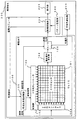
本発明を好適に実施した第1の実施形態について説明する。図1に本実施形態にかかる撮像素子の構成を示す。撮像素子100は、CCDセンサ101、X方向コントローラ103、Y方向コントローラ104、可視光受信制御部105、A/D変換器106及び電荷電圧変換器109を有する。
CCDセンサ101は、複数のフォトダイオード(PD)が縦横に整列しており、各PDにおいて発生した電荷を電荷電圧変換部109を介してA/D106へ転送するためのCCDを備えている。CCDによってPDから取り出された電荷は、シリアルに(換言すると、時分割されて)電荷電圧変換部109へ入力され、電荷に応じたアナログ電気信号に変換されてA/D106へ入力される。制御部102は、CCDセンサ101にスキャンを行わせる(各PDから所定の順序で電荷を転送させる)ための機能部であり、CCD101のPDから所定の順序で電荷が転送されるようにX方向コントローラ103及びY方向コントローラ104を駆動する。X方向コントローラ103はCCDセンサ101のどの列のPDの電荷を電荷電圧変換器109へ転送するかを指定するための機能部である。Y方向コントローラ104は、CCDセンサ101のどの行のPDの電荷を転送するのかを指定するための機能部である。X方向コントローラ103及びY方向コントローラ104の出力の組み合わせにより、一又は複数の任意の行のPDが発生させた電荷を電荷電圧変換器109へ出力できる。なお、複数個の行のPDを指定した場合には、指定された行の全てのPDの電荷が電荷電圧変換器109へ転送される。可視光受信制御部105は、可視光通信時に、所定のタイミングで特定の行のPD(可視光信号受光用PD)の電荷を電荷電圧変換器109へ転送させる機能部である。A/D106は、CCDセンサ101から転送されてきた電荷量(換言すると、電流値)に基づいて電荷電圧変換器109が生成したアナログ信号をデジタル信号に変換する。なお、通常のスキャン動作中は可視光受信制御部105はA/D106へ同期信号を出力していないため、可視光信号受光用PDから転送された電荷に応じたデジタル信号は、映像信号としてA/D106から出力される。また、複数の行のPDから電荷が入力された場合には、入力された電荷の平均値に応じたデジタル信号を出力する。
[First Embodiment]
A first embodiment in which the present invention is suitably implemented will be described. FIG. 1 shows a configuration of an image sensor according to the present embodiment. The
The CCD sensor 101 includes a plurality of photodiodes (PDs) arranged vertically and horizontally, and a CCD for transferring charges generated in each PD to the A /
撮像素子100の動作について説明する。可視光受信制御部105は、可視光通信時には所定のタイミングでX方向コントローラ103及びY方向コントローラ104に制御信号を出力して、可視光信号受光用PDを含む行の電荷を電荷電圧変換器109へ転送させる。
The operation of the
例えば、可視光受信制御部105は、可視光信号受光用PDを含む行の電荷を電荷電圧変換器109へ転送するための制御信号を、CCDセンサ101が1行分のPDの電荷を電荷電圧変換器109へ転送するごとにX方向コントローラ103及びY方向コントローラ104へ出力する。これにより、1行分のPDの電荷が電荷電圧変換器109へ出力されるごとに可視光信号受光用PDを含む行のみの電荷が電荷電圧変換器109へ出力されるようになる。
For example, the visible light
これにより、図2に示すように、N行並んだPDを備えたCCDセンサ101であれば、フレームレートのN倍の周期で可視光信号をサンプリングできる。よって、単位時間当たりの通信速度を高めることが可能となる。 Thereby, as shown in FIG. 2, the CCD sensor 101 having PDs arranged in N rows can sample a visible light signal at a cycle of N times the frame rate. Therefore, it is possible to increase the communication speed per unit time.
また、図3に示すように、第2のA/DコンバータであるA/D2 108を追加し、映像信号と、可視光信号をそれぞれ別のA/DコンバータでA/D変換してもよい。このような構成をとれば、映像信号および可視光信号に最適な特性を持つA/Dコンバータを使用できるという利点がある。 In addition, as shown in FIG. 3, a second A / D converter A / D2 108 may be added, and the video signal and the visible light signal may be A / D converted by separate A / D converters. . With such a configuration, there is an advantage that an A / D converter having optimum characteristics for a video signal and a visible light signal can be used.
〔第2の実施形態〕
本発明を好適に実施した第2の実施形態について説明する。図4に、本実施形態にかかる撮像素子の構成を示す。本実施形態の撮像素子100は、第1の実施形態にかかる撮像素子100とほぼ同様の構成であるが、可視光信号認識部107をさらに有する。
[Second Embodiment]
A second embodiment in which the present invention is suitably implemented will be described. FIG. 4 shows the configuration of the image sensor according to the present embodiment. The
可視光信号認識部107は、A/D106から出力された可視光信号受光用PDの出力を所定回数分蓄積するキャッシュメモリを備えている。可視光信号認識部107は、A/D106から可視光信号受光用PDの出力が入力された際には、キャッシュメモリに蓄積されているデータ(可視光信号受光用PDの出力履歴)と新たにA/D106から入力されたデジタル信号(可視光信号受光用PDの出力に応じてA/D106から出力されたデジタル信号)とに基づいて、可視光信号受光用PDが可視光情報を受信しているか否かを判断する。可視光情報認識部107は、可視光情報受光用PDが可視光情報を受信していると判断した場合には、可視光受信制御部105へ制御信号を出力し、制御部102によるスキャンを停止させる。
The visible light signal recognition unit 107 includes a cache memory that accumulates the output of the visible light signal receiving PD output from the A / D 106 a predetermined number of times. When the output of the visible light signal receiving PD is input from the A /
図5に、本実施形態にかかる撮像素子の動作の流れを示す。
制御部102は、X方向コントローラ103及びY方向コントローラ104を駆動して、CCDセンサ101の各PDから所定の順序で電荷を転送していく(ステップS201)。第1の実施形態と同様に、所定のタイミング(例えば、1行スキャンするごと)で可視光信号受光用PDの電荷に応じたアナログ信号が電荷電圧変換器109において生成され、A/D106へ転送される(ステップS202)。A/D106は可視光信号受光用PDから出力されてきた電荷に応じたアナログ信号をデジタル信号に変換し、可視光信号認識部107へ出力する。
FIG. 5 shows a flow of operations of the image sensor according to the present embodiment.
The
可視光信号認識部107は、A/D106から入力されたデジタル信号を不図示のキャッシュに蓄積する(ステップS203)。そして、可視光信号認識部107は、可視光信号受光用PDが可視光信号を受光しているか否かを判断する(ステップS204)。例えば、可視光信号受光用PDが出力する電荷に変化が無い場合(2値信号であれば、A/D106からの出力信号が“0”又は“1”のまま変化していない場合)、可視光信号認識部107は、可視光信号受光用PDが可視光信号を受光していないと判断する(ステップS204/No)。この場合は、通常のスキャン動作を継続する。
一方、可視光受光用PDが可視光信号を受光していると判断した場合(ステップS204/Yes)、可視光信号認識部107は、可視光受信制御部105へ制御信号を出力し、スキャン動作を停止させる(ステップS205)。スキャン動作停止後は、可視光受信制御部105は、所定のタイミングで可視光信号の存在する行のみの可視光信号受光用PDの電荷を電荷電圧変換器109に転送してアナログ信号を生成させ、そのアナログ信号をA/D106へ転送し、可視光信号を受光する。この動作は、上記第1の実施形態と同様であるため、重複する説明は省略する。
The visible light signal recognition unit 107 accumulates the digital signal input from the A /
On the other hand, when it is determined that the visible light receiving PD receives a visible light signal (step S204 / Yes), the visible light signal recognition unit 107 outputs a control signal to the visible light
このように、本実施形態にかかる撮像素子は、可視光信号受光用PDが可視光信号を受信していると判断した場合には通常のスキャン動作を停止させるため、可視光通信時の消費電力を低減できる。 As described above, the imaging device according to the present embodiment stops the normal scanning operation when it is determined that the visible light signal receiving PD receives the visible light signal, so that the power consumption during visible light communication is reduced. Can be reduced.
なお、本実施形態にかかる撮像素子を備えた携帯端末は、可視光受信制御部105がスキャン動作を停止させた場合には、可視光通信中であるメッセージを表示すると良い。
In addition, the portable terminal provided with the image sensor according to the present embodiment may display a message indicating that visible light communication is being performed when the visible light
〔第3の実施形態〕
本発明を好適に実施した第3の実施形態について説明する。図6に本実施形態にかかる携帯端末の構成を示す。携帯端末200は、撮像素子100、画像認識部201、パターン記憶部202、表示部203及び可視光通信部204を有する。なお、撮像素子100、画像認識部201及びパターン記憶部202は、光電変換素子に光を集光する為の不図示のレンズなどとともにモジュールとして一体に構成されている。
[Third Embodiment]
A third embodiment in which the present invention is preferably implemented will be described. FIG. 6 shows the configuration of the mobile terminal according to the present embodiment. The
撮像素子100は、第1の実施形態において説明したものと同様である。画像認識部201は、A/D106から出力された1フレーム分の映像信号を解析して、フレーム画像中に(すなわち、被写体に)所定の形状の部分が存在するか否かを判断する。画像認識部201は、フレーム画像中に所定形状の部分が存在すると判断した場合には、可視光受信制御部105へ制御信号を出力し、特定のPDを可視光信号検出用PDとして選択して所定の周期で電荷を電荷電圧変換器109へ転送させ、電荷に応じたアナログ信号を電荷電圧変換器109からA/D106へ転送させる。画像認識部201は、パターン記憶部202に記憶されている形状とフレーム画像とを比較することによって、フレーム画像中に所定の形状の部分が存在するか否かを判断する。パターン記憶部202には、特定の形状のデータが記憶されている。表示部203は、A/D106から出力される映像信号に応じた画像を表示する装置であり、例えばLCDである。可視光通信部204は、A/D106から出力される可視光信号に応じたデジタル信号を処理する。
The
携帯端末200は、この他に携帯端末としての機能を司る機能部(例えば、携帯電話端末であれば無線回路やアンテナなど)を備えるが、これらは公知のものを適用可能であるため、図中には示さず説明は省略する。
In addition to this, the
本実施形態にかかる携帯端末の可視光通信時の動作について説明する。図7に、携帯端末200の可視光通信時の動作の流れを示す。
制御部102は、X方向コントローラ103及びY方向コントローラ104を駆動して、CCDセンサ101の各PDの電荷を順次電荷電圧変換器109へ転送し、電荷に応じたアナログ信号をA/D106へ出力させる(ステップS301)。画像認識部201は、A/D106から入力されるデジタル信号を1フレーム分ラッチしてフレーム画像のデータを生成する。そして、画像認識部201は、パターン記憶部202に記憶されている形状データを読み出し、生成したフレーム画像の中に読み出したパターンと一致する部分があるか否かを判断する(ステップS302)。
An operation at the time of visible light communication of the mobile terminal according to the present embodiment will be described. FIG. 7 shows a flow of operations of the
The
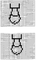
図8(a)に示す形状データがパターン記憶部に202に記憶されている場合、(b)に示すようなフレーム画像が得られたならば、パターンと一致する部分があると判断する。なお(c)に示すように、パターンと一致する部分はフレーム画像の周縁部に合っても良い。
When the shape data shown in FIG. 8A is stored in the
パターン記憶部202から読み出した形状と一致する部分があると判断した場合には(ステップS302/Yes)、画像認識部201は可視光受信制御部105へ制御信号を送り、可視光信号受光用PDを指定する。例えば、図8(b)や(c)に示すようなフレーム画像が得られたのであれば、三重の閉曲線の内側にあるPDを可視光信号受光用PDとして指定する。画像認識部201からの制御信号を受信した可視光受信制御部105は、指定されたPDを可視光信号受光用PDとして、その可視光信号の存在する行のみPDの電荷を所定の周期で電荷電圧変換器109へ転送する動作をX方向コントローラ103及びY方向コントローラ104に行わせる(ステップS303)。
一方、一致する部分が無いと判断した場合には(ステップS302/No)、画像認識部201は、可視光受信制御部105へ制御信号を送らず、通常のスキャン動作を実行させる。
If it is determined that there is a part that matches the shape read from the pattern storage unit 202 (Yes in step S302), the
On the other hand, if it is determined that there is no matching portion (step S302 / No), the
このように、本実施形態にかかる携帯端末は、1フレームの画像中に含まれる特定の形状を認識して、可視光信号の受光に用いるPDを自動的に選択する。これにより、可視光信号を受光する際に、可視光信号が特定のPDに受光されるようにユーザが端末の向きを調整する手間が不必要となる。 As described above, the mobile terminal according to the present embodiment recognizes a specific shape included in an image of one frame and automatically selects a PD used for receiving a visible light signal. This eliminates the need for the user to adjust the orientation of the terminal so that the visible light signal is received by the specific PD when receiving the visible light signal.
なお、画像認識部201に手ぶれ検出機能を持たせてもよい。すなわち、画像認識部201にフレーム画像をキャッシュする機能を設け、一つ前のフレームと比較して画像全体が同一方向にシフトした場合には、可視光信号受光用のPDもシフトさせる。例えば図9に示すように、画像全体が上方向及び左方向に各2画素ずれた場合には、元の可視光信号受光用PDから上方向及び左方向にそれぞれ2画素の位置にあるPDを可視光信号受光用PDとして用いる。これにより、可視光信号受光中に携帯端末の位置がずれたとしても、可視光通信を継続して行えるようになる。
Note that the
〔第4の実施形態〕
本発明を好適に実施した第4の実施形態にかかる携帯端末の構成を示す。図10に本実施形態にかかる携帯端末の構成を示す。本実施形態にかかる携帯端末200は、第3の実施形態のものとほぼ同様であるが、パターン記憶部202を備えていない。
本実施形態において画像認識部201はフレーム画像をキャッシュする機能を備えており、一つ前のフレームと比較して受光量が所定量以上変化したPDがあるか否かを検出する。画像認識部201は、受光量が所定量以上変化したPDがある場合には、制御信号を可視光受信部105へ出力し、そのPDを可視光信号受光用PDとして指定する。
[Fourth Embodiment]
The structure of the portable terminal concerning 4th Embodiment which implemented this invention suitably is shown. FIG. 10 shows the configuration of the mobile terminal according to the present embodiment. The
In the present embodiment, the
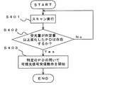
本実施形態にかかる携帯端末200の可視光通信時の動作について説明する。図11に、携帯端末200の可視光通信時の動作の流れを示す。
制御部102は、X方向コントローラ103及びY方向コントローラ104を駆動して、CCDセンサ101の各PDの電荷を順次電荷電圧変換器109へ転送し、電荷に応じたアナログ信号をA/D106へ出力させる(ステップS401)。画像認識部201は、A/D106から入力されるデジタル信号を1フレーム分ラッチしてフレーム画像のデータを生成する。そして、画像認識部201は、キャッシュしている前回のフレーム画像データを読み出し、生成したフレーム画像の中に前回のフレーム画像と比較して受光量が所定量以上変化した部分があるか否かを判断する(ステップS402)。
An operation at the time of visible light communication of the
The
受光量が所定量以上変化した部分がある場合には(ステップS402/Yes)、画像認識部201は可視光受信制御部105へ制御信号を送り、その部分に該当するPDを可視光信号受光用PDとして指定する。画像認識部201からの制御信号を受信した可視光受信制御部105は、指定されたPDを可視光信号受光用PDとして、その可視光信号の存在する行のみPDの電荷を所定の周期で電荷電圧変換器109へ転送する動作をX方向コントローラ103及びY方向コントローラ104に行わせる(ステップS403)。
一方、受光量が所定量以上変化した部分が無い場合には(ステップS402/No)、画像認識部201は、可視光受信制御部105へ制御信号を送らず、通常のスキャン動作を実行させる。
When there is a portion where the amount of received light has changed by a predetermined amount or more (step S402 / Yes), the
On the other hand, if there is no portion where the amount of received light has changed by a predetermined amount or more (step S402 / No), the
なお、受光量が所定量以上変化した部分が複数ある場合には、各箇所について上記の処理を順番に実行すれば良い。 In addition, when there are a plurality of portions where the amount of received light has changed by a predetermined amount or more, the above processing may be executed in order for each portion.
このように、本実施形態にかかる携帯端末は、1フレームの画像中に受光量が所定量以上変化した部分があるか否かを判断して、可視光信号の受光に用いるPDを自動的に選択する。これにより、可視光信号を受光する際に、可視光信号が特定のPDに受光されるようにユーザが端末の向きを調整する手間が不必要となる。 As described above, the mobile terminal according to the present embodiment automatically determines the PD used to receive the visible light signal by determining whether or not there is a portion in which the light reception amount has changed by a predetermined amount or more in one frame image. select. This eliminates the need for the user to adjust the orientation of the terminal so that the visible light signal is received by the specific PD when receiving the visible light signal.
なお、上記各実施形態は本発明の好適な実施の一例であり、本発明はこれに限定されることはない。
例えば、上記各実施形態においては、可視光信号をサンプリングする周期は一定であったが、サンプリング周期が必ずしも一定である必要はない。
また、上記各実施形態は単色の画像信号を生成するCCDセンサを用いる構成を示したが、カラー画像信号を生成するCCDセンサを用いても良い。この場合には、RGBの全てに本発明を適用する必要はなく、少なくとも一色に適用すればよい。
このように、本発明は様々な変形が可能である。
Each of the above embodiments is an example of a preferred embodiment of the present invention, and the present invention is not limited to this.
For example, in each of the above embodiments, the period for sampling the visible light signal is constant, but the sampling period is not necessarily constant.
Moreover, although each said embodiment showed the structure which uses the CCD sensor which produces | generates a monochrome image signal, you may use the CCD sensor which produces | generates a color image signal. In this case, it is not necessary to apply the present invention to all of RGB, and it may be applied to at least one color.
As described above, the present invention can be variously modified.
100 撮像素子
101 CCDセンサ
102 制御部
103 X方向コントローラ
104 Y方向コントローラ
105 可視光受信制御部
106 A/D
107 可視光信号認識部
108 A/D 2
109 電荷電圧変換器
200 携帯端末
201 画像認識部
202 パターン記憶部
203 表示部
204 可視光通信部
DESCRIPTION OF
107 Visible Light Signal Recognition Unit 108 A /
109
Claims (13)
特定の光電変換素子からは前記第1の周期よりも早い第2の周期で前記デジタル信号生成手段へ電荷を転送させる手段を備え、
前記デジタル信号生成手段は、前記第1の期間を周期として前記特定の光電変換素子から転送されてきた電荷に応じて前記第1のデジタル信号として出力し、前記第2の期間を周期として前記特定の光電変換素子から転送されてきた電荷に応じて、第2のデジタル信号として前記第1のデジタル信号とは異なる経路へ出力することを特徴とする撮像素子。 And regularly arranged a plurality of photoelectric conversion elements, the photoelectric charge transfer means converting element to transfer the generated charges from the photoelectric conversion element, a digital signal based on is manner was charge amount transferred from the photoelectric conversion element and a digital signal generating means for generating, transfers the electric load that is respectively generated in the photoelectric conversion element to said digital signal generating means in a predetermined order a first time period as a period from the digital signal generating means An image sensor that outputs a first digital signal,
Et whether a particular photoelectric conversion element is provided with means for transferring the charges to the digital signal generating means in the early second period than the first period,
It said digital signal generation means outputs said first period depending on the charge transferred from a particular photoelectric conversion element as the period as the first digital signal, the said second time period as the period depending on the charge transferred from a particular photoelectric conversion element, an imaging device and outputting to a path different from said as a second digital signal the first digital signal.
さらに第2のデジタル信号生成手段を有し、
特定の光電変換素子からは前記第1の周期よりも早い第2の周期で前記第2のデジタル信号生成手段へ電荷を転送させる手段を備え、
前記第1のデジタル信号生成手段は、前記第1の期間を周期として前記特定の光電変換素子から転送されてきた電荷に応じて前記第1のデジタル信号として出力し、
前記第2のデジタル信号生成手段は、前記第2の期間を周期として前記特定の光電変換素子から転送されてきた電荷に応じて、第2のデジタル信号として前記第1のデジタル信号とは異なる経路へ出力することを特徴とする撮像素子。 And regularly arranged a plurality of photoelectric conversion elements, the photoelectric charge transfer means converting element to transfer the generated charges from the photoelectric conversion element, a digital signal based on is manner was charge amount transferred from the photoelectric conversion element and a first digital signal generating means for generating, transfers the electric load that is respectively generated in the photoelectric conversion element to the a predetermined order a first time period as the period first digital signal generator, An image sensor that outputs a first digital signal from the first digital signal generating means ,
Furthermore, it has a second digital signal generation means ,
Et whether a particular photoelectric conversion element is provided with means for transferring charges to said second digital signal generating means in the early second period than the first period,
The first digital signal generation means outputs said first period depending on the charge transferred from a particular photoelectric conversion element as the period as the first digital signal,
Said second digital signal generating means, said depending on the charge transferred from a particular photoelectric conversion element and the second period as a period, different from the first digital signal as a second digital signal An image sensor that outputs to a path.
Priority Applications (1)
| Application Number | Priority Date | Filing Date | Title |
|---|---|---|---|
| JP2004307737A JP4736397B2 (en) | 2004-10-22 | 2004-10-22 | Imaging device, imaging module, and portable terminal |
Applications Claiming Priority (1)
| Application Number | Priority Date | Filing Date | Title |
|---|---|---|---|
| JP2004307737A JP4736397B2 (en) | 2004-10-22 | 2004-10-22 | Imaging device, imaging module, and portable terminal |
Related Child Applications (1)
| Application Number | Title | Priority Date | Filing Date |
|---|---|---|---|
| JP2006340565A Division JP2007151143A (en) | 2006-12-18 | 2006-12-18 | Imaging device, imaging module and mobile terminal |
Publications (2)
| Publication Number | Publication Date |
|---|---|
| JP2006121466A JP2006121466A (en) | 2006-05-11 |
| JP4736397B2 true JP4736397B2 (en) | 2011-07-27 |
Family
ID=36538925
Family Applications (1)
| Application Number | Title | Priority Date | Filing Date |
|---|---|---|---|
| JP2004307737A Expired - Fee Related JP4736397B2 (en) | 2004-10-22 | 2004-10-22 | Imaging device, imaging module, and portable terminal |
Country Status (1)
| Country | Link |
|---|---|
| JP (1) | JP4736397B2 (en) |
Cited By (17)
| Publication number | Priority date | Publication date | Assignee | Title |
|---|---|---|---|---|
| CN103650384A (en) * | 2012-05-24 | 2014-03-19 | 松下电器产业株式会社 | information communication method |
| US9407368B2 (en) | 2012-12-27 | 2016-08-02 | Panasonic Intellectual Property Corporation Of America | Information communication method |
| US9462173B2 (en) | 2012-12-27 | 2016-10-04 | Panasonic Intellectual Property Corporation Of America | Information communication method |
| US9467225B2 (en) | 2012-12-27 | 2016-10-11 | Panasonic Intellectual Property Corporation Of America | Information communication method |
| US9515731B2 (en) | 2012-12-27 | 2016-12-06 | Panasonic Intellectual Property Corporation Of America | Information communication method |
| US9560284B2 (en) | 2012-12-27 | 2017-01-31 | Panasonic Intellectual Property Corporation Of America | Information communication method for obtaining information specified by striped pattern of bright lines |
| US9564970B2 (en) | 2012-12-27 | 2017-02-07 | Panasonic Intellectual Property Corporation Of America | Information communication method for obtaining information using ID list and bright line image |
| US9591232B2 (en) | 2012-12-27 | 2017-03-07 | Panasonic Intellectual Property Corporation Of America | Information communication method |
| US9608725B2 (en) | 2012-12-27 | 2017-03-28 | Panasonic Intellectual Property Corporation Of America | Information processing program, reception program, and information processing apparatus |
| US9608727B2 (en) | 2012-12-27 | 2017-03-28 | Panasonic Intellectual Property Corporation Of America | Switched pixel visible light transmitting method, apparatus and program |
| US9613596B2 (en) | 2012-12-27 | 2017-04-04 | Panasonic Intellectual Property Corporation Of America | Video display method using visible light communication image including stripe patterns having different pitches |
| US9646568B2 (en) | 2012-12-27 | 2017-05-09 | Panasonic Intellectual Property Corporation Of America | Display method |
| US9918016B2 (en) | 2012-12-27 | 2018-03-13 | Panasonic Intellectual Property Corporation Of America | Information communication apparatus, method, and recording medium using switchable normal mode and visible light communication mode |
| US10303945B2 (en) | 2012-12-27 | 2019-05-28 | Panasonic Intellectual Property Corporation Of America | Display method and display apparatus |
| US10523876B2 (en) | 2012-12-27 | 2019-12-31 | Panasonic Intellectual Property Corporation Of America | Information communication method |
| US10530486B2 (en) | 2012-12-27 | 2020-01-07 | Panasonic Intellectual Property Corporation Of America | Transmitting method, transmitting apparatus, and program |
| US10951310B2 (en) | 2012-12-27 | 2021-03-16 | Panasonic Intellectual Property Corporation Of America | Communication method, communication device, and transmitter |
Families Citing this family (15)
| Publication number | Priority date | Publication date | Assignee | Title |
|---|---|---|---|---|
| JP4726559B2 (en) * | 2005-07-12 | 2011-07-20 | シャープ株式会社 | Optical signal receiving apparatus and portable information communication terminal having the apparatus |
| JP4802033B2 (en) * | 2006-04-18 | 2011-10-26 | 大宏電機株式会社 | Light receiver for spatial light communication |
| JP5339049B2 (en) * | 2008-11-28 | 2013-11-13 | カシオ計算機株式会社 | Information restoration apparatus, information restoration method, and program |
| JP5282899B2 (en) * | 2009-03-19 | 2013-09-04 | カシオ計算機株式会社 | Information restoration apparatus and information restoration method |
| EP2538584B1 (en) | 2011-06-23 | 2018-12-05 | Casio Computer Co., Ltd. | Information Transmission System, and Information Transmission Method |
| JP5294096B2 (en) * | 2011-06-23 | 2013-09-18 | カシオ計算機株式会社 | Information transmission system, light receiving device, information transmission method, and program |
| JP5530578B1 (en) * | 2012-12-27 | 2014-06-25 | パナソニック株式会社 | Information communication method |
| EP2940897B1 (en) * | 2012-12-27 | 2020-03-11 | Panasonic Intellectual Property Corporation of America | Information communication method |
| SG11201504988UA (en) * | 2012-12-27 | 2015-07-30 | Panasonic Ip Corp America | Information communication method |
| WO2014103329A1 (en) | 2012-12-27 | 2014-07-03 | パナソニック株式会社 | Visible-light-communication-signal display method and display device |
| EP2940903B1 (en) * | 2012-12-27 | 2021-05-12 | Panasonic Intellectual Property Corporation of America | Information communication method |
| CN104871455B (en) * | 2012-12-27 | 2018-11-30 | 松下电器(美国)知识产权公司 | Information communicating method |
| JP6653128B2 (en) * | 2014-05-16 | 2020-02-26 | 株式会社Gocco. | Visible light communication system |
| CN107466477B (en) | 2015-11-12 | 2021-08-10 | 松下电器(美国)知识产权公司 | Display method, computer-readable recording medium, and display device |
| JP7146483B2 (en) * | 2018-06-27 | 2022-10-04 | ソニーセミコンダクタソリューションズ株式会社 | Light receiving device, its control method, and electronic device |
Family Cites Families (4)
| Publication number | Priority date | Publication date | Assignee | Title |
|---|---|---|---|---|
| JP4153064B2 (en) * | 1997-11-19 | 2008-09-17 | 浜松ホトニクス株式会社 | Photodetection element and tracking sensor device |
| JP3592147B2 (en) * | 1998-08-20 | 2004-11-24 | キヤノン株式会社 | Solid-state imaging device |
| JP2001285684A (en) * | 2000-03-30 | 2001-10-12 | Minolta Co Ltd | Electronic camera |
| JP2004180187A (en) * | 2002-11-29 | 2004-06-24 | Hitachi Ltd | Space division infrared communication system |
-
2004
- 2004-10-22 JP JP2004307737A patent/JP4736397B2/en not_active Expired - Fee Related
Cited By (54)
| Publication number | Priority date | Publication date | Assignee | Title |
|---|---|---|---|---|
| CN103650384A (en) * | 2012-05-24 | 2014-03-19 | 松下电器产业株式会社 | information communication method |
| US9456109B2 (en) | 2012-05-24 | 2016-09-27 | Panasonic Intellectual Property Corporation Of America | Information communication method of obtaining information from a subject by demodulating data specified by a pattern of a bright line included in an obtained image |
| CN103650384B (en) * | 2012-05-24 | 2017-07-18 | 松下电器(美国)知识产权公司 | information communication method |
| US10218914B2 (en) | 2012-12-20 | 2019-02-26 | Panasonic Intellectual Property Corporation Of America | Information communication apparatus, method and recording medium using switchable normal mode and visible light communication mode |
| US9407368B2 (en) | 2012-12-27 | 2016-08-02 | Panasonic Intellectual Property Corporation Of America | Information communication method |
| US9450672B2 (en) | 2012-12-27 | 2016-09-20 | Panasonic Intellectual Property Corporation Of America | Information communication method of transmitting a signal using change in luminance |
| US9462173B2 (en) | 2012-12-27 | 2016-10-04 | Panasonic Intellectual Property Corporation Of America | Information communication method |
| US9467225B2 (en) | 2012-12-27 | 2016-10-11 | Panasonic Intellectual Property Corporation Of America | Information communication method |
| US9515731B2 (en) | 2012-12-27 | 2016-12-06 | Panasonic Intellectual Property Corporation Of America | Information communication method |
| US9560284B2 (en) | 2012-12-27 | 2017-01-31 | Panasonic Intellectual Property Corporation Of America | Information communication method for obtaining information specified by striped pattern of bright lines |
| US9564970B2 (en) | 2012-12-27 | 2017-02-07 | Panasonic Intellectual Property Corporation Of America | Information communication method for obtaining information using ID list and bright line image |
| US9571191B2 (en) | 2012-12-27 | 2017-02-14 | Panasonic Intellectual Property Corporation Of America | Information communication method |
| US9591232B2 (en) | 2012-12-27 | 2017-03-07 | Panasonic Intellectual Property Corporation Of America | Information communication method |
| US9608725B2 (en) | 2012-12-27 | 2017-03-28 | Panasonic Intellectual Property Corporation Of America | Information processing program, reception program, and information processing apparatus |
| US9608727B2 (en) | 2012-12-27 | 2017-03-28 | Panasonic Intellectual Property Corporation Of America | Switched pixel visible light transmitting method, apparatus and program |
| US9613596B2 (en) | 2012-12-27 | 2017-04-04 | Panasonic Intellectual Property Corporation Of America | Video display method using visible light communication image including stripe patterns having different pitches |
| US9635278B2 (en) | 2012-12-27 | 2017-04-25 | Panasonic Intellectual Property Corporation Of America | Information communication method for obtaining information specified by striped pattern of bright lines |
| US9641766B2 (en) | 2012-12-27 | 2017-05-02 | Panasonic Intellectual Property Corporation Of America | Information communication method |
| US9646568B2 (en) | 2012-12-27 | 2017-05-09 | Panasonic Intellectual Property Corporation Of America | Display method |
| US9756255B2 (en) | 2012-12-27 | 2017-09-05 | Panasonic Intellectual Property Corporation Of America | Information communication method |
| US9768869B2 (en) | 2012-12-27 | 2017-09-19 | Panasonic Intellectual Property Corporation Of America | Information communication method |
| US9794489B2 (en) | 2012-12-27 | 2017-10-17 | Panasonic Intellectual Property Corporation Of America | Information communication method |
| US9859980B2 (en) | 2012-12-27 | 2018-01-02 | Panasonic Intellectual Property Corporation Of America | Information processing program, reception program, and information processing apparatus |
| US9918016B2 (en) | 2012-12-27 | 2018-03-13 | Panasonic Intellectual Property Corporation Of America | Information communication apparatus, method, and recording medium using switchable normal mode and visible light communication mode |
| US9998220B2 (en) | 2012-12-27 | 2018-06-12 | Panasonic Intellectual Property Corporation Of America | Transmitting method, transmitting apparatus, and program |
| US10051194B2 (en) | 2012-12-27 | 2018-08-14 | Panasonic Intellectual Property Corporation Of America | Information communication method |
| US10148354B2 (en) | 2012-12-27 | 2018-12-04 | Panasonic Intellectual Property Corporation Of America | Luminance change information communication method |
| US10165192B2 (en) | 2012-12-27 | 2018-12-25 | Panasonic Intellectual Property Corporation Of America | Information communication method |
| US10205887B2 (en) | 2012-12-27 | 2019-02-12 | Panasonic Intellectual Property Corporation Of America | Information communication method |
| US10225014B2 (en) | 2012-12-27 | 2019-03-05 | Panasonic Intellectual Property Corporation Of America | Information communication method for obtaining information using ID list and bright line image |
| US10303945B2 (en) | 2012-12-27 | 2019-05-28 | Panasonic Intellectual Property Corporation Of America | Display method and display apparatus |
| US10334177B2 (en) | 2012-12-27 | 2019-06-25 | Panasonic Intellectual Property Corporation Of America | Information communication apparatus, method, and recording medium using switchable normal mode and visible light communication mode |
| US10354599B2 (en) | 2012-12-27 | 2019-07-16 | Panasonic Intellectual Property Corporation Of America | Display method |
| US10361780B2 (en) | 2012-12-27 | 2019-07-23 | Panasonic Intellectual Property Corporation Of America | Information processing program, reception program, and information processing apparatus |
| US10368005B2 (en) | 2012-12-27 | 2019-07-30 | Panasonic Intellectual Property Corporation Of America | Information communication method |
| US10368006B2 (en) | 2012-12-27 | 2019-07-30 | Panasonic Intellectual Property Corporation Of America | Information communication method |
| US10447390B2 (en) | 2012-12-27 | 2019-10-15 | Panasonic Intellectual Property Corporation Of America | Luminance change information communication method |
| US10455161B2 (en) | 2012-12-27 | 2019-10-22 | Panasonic Intellectual Property Corporation Of America | Information communication method |
| US10516832B2 (en) | 2012-12-27 | 2019-12-24 | Panasonic Intellectual Property Corporation Of America | Information communication method |
| US10521668B2 (en) | 2012-12-27 | 2019-12-31 | Panasonic Intellectual Property Corporation Of America | Display method and display apparatus |
| US10523876B2 (en) | 2012-12-27 | 2019-12-31 | Panasonic Intellectual Property Corporation Of America | Information communication method |
| US10531009B2 (en) | 2012-12-27 | 2020-01-07 | Panasonic Intellectual Property Corporation Of America | Information communication method |
| US10531010B2 (en) | 2012-12-27 | 2020-01-07 | Panasonic Intellectual Property Corporation Of America | Information communication method |
| US10530486B2 (en) | 2012-12-27 | 2020-01-07 | Panasonic Intellectual Property Corporation Of America | Transmitting method, transmitting apparatus, and program |
| US10616496B2 (en) | 2012-12-27 | 2020-04-07 | Panasonic Intellectual Property Corporation Of America | Information communication method |
| US10638051B2 (en) | 2012-12-27 | 2020-04-28 | Panasonic Intellectual Property Corporation Of America | Information communication method |
| US10666871B2 (en) | 2012-12-27 | 2020-05-26 | Panasonic Intellectual Property Corporation Of America | Information communication method |
| US10742891B2 (en) | 2012-12-27 | 2020-08-11 | Panasonic Intellectual Property Corporation Of America | Information communication method |
| US10887528B2 (en) | 2012-12-27 | 2021-01-05 | Panasonic Intellectual Property Corporation Of America | Information communication method |
| US10951310B2 (en) | 2012-12-27 | 2021-03-16 | Panasonic Intellectual Property Corporation Of America | Communication method, communication device, and transmitter |
| US11165967B2 (en) | 2012-12-27 | 2021-11-02 | Panasonic Intellectual Property Corporation Of America | Information communication method |
| US11490025B2 (en) | 2012-12-27 | 2022-11-01 | Panasonic Intellectual Property Corporation Of America | Information communication method |
| US11659284B2 (en) | 2012-12-27 | 2023-05-23 | Panasonic Intellectual Property Corporation Of America | Information communication method |
| US12088923B2 (en) | 2012-12-27 | 2024-09-10 | Panasonic Intellectual Property Corporation Of America | Information communication method |
Also Published As
| Publication number | Publication date |
|---|---|
| JP2006121466A (en) | 2006-05-11 |
Similar Documents
| Publication | Publication Date | Title |
|---|---|---|
| JP4736397B2 (en) | Imaging device, imaging module, and portable terminal | |
| US9060126B2 (en) | Solid-state image sensing apparatus | |
| KR101166461B1 (en) | A/d conversion apparatus, solid-state image capturing apparatus and electronic information device | |
| EP2587407B1 (en) | Vision recognition apparatus and method | |
| US7936394B2 (en) | Mobile devices having an image sensor for charging a battery | |
| KR20170006206A (en) | Image Sensor Having Wide Dynamic Range, Pixel Circuit Of Image Sensor and Operating Method Thereof | |
| JP2009212909A (en) | Solid-state imaging apparatus, flicker detection method for solid-state imaging apparatus, control program, readable recording medium, and electronic information device | |
| US9866776B2 (en) | Image sensor, image capturing apparatus, and cellular phone | |
| CN114422725B (en) | Image output method, image sensor and application thereof | |
| US20160044262A1 (en) | Solid-state imaging device and driving method thereof, and electronic apparatus using the same | |
| JPWO2015045704A1 (en) | Imaging apparatus and focus control method | |
| KR20180031288A (en) | Image sensor and imaging device including the same | |
| CN100473121C (en) | Image Pixels of CMOS Image Sensors | |
| KR20120019178A (en) | Wide dynamic range image sensor, pixel array of image sensor and driving method of image sensor | |
| US10861885B1 (en) | Method of obtaining image data and related image sensing system | |
| KR20210003918A (en) | Image sensor | |
| JP2007151143A (en) | Imaging device, imaging module and mobile terminal | |
| JP4334950B2 (en) | Solid-state imaging device | |
| US20210185259A1 (en) | Image sensor, imaging device including image sensor, and method of operating imaging device | |
| JP5274169B2 (en) | Imaging device | |
| EP1805801B1 (en) | Image sensor with expanding dynamic range | |
| JP7325211B2 (en) | IMAGING DEVICE AND CONTROL METHOD THEREOF, PROGRAM, STORAGE MEDIUM | |
| JP3668604B2 (en) | Solid-state image sensor and image system using the same | |
| JP4389347B2 (en) | Image sensor with calculation function | |
| JP2006352758A (en) | Image signal processing device |
Legal Events
| Date | Code | Title | Description |
|---|---|---|---|
| A621 | Written request for application examination |
Free format text: JAPANESE INTERMEDIATE CODE: A621 Effective date: 20060313 |
|
| A977 | Report on retrieval |
Free format text: JAPANESE INTERMEDIATE CODE: A971007 Effective date: 20081219 |
|
| A131 | Notification of reasons for refusal |
Free format text: JAPANESE INTERMEDIATE CODE: A131 Effective date: 20090324 |
|
| A521 | Request for written amendment filed |
Free format text: JAPANESE INTERMEDIATE CODE: A523 Effective date: 20090519 |
|
| A131 | Notification of reasons for refusal |
Free format text: JAPANESE INTERMEDIATE CODE: A131 Effective date: 20100330 |
|
| A521 | Request for written amendment filed |
Free format text: JAPANESE INTERMEDIATE CODE: A523 Effective date: 20100527 |
|
| A01 | Written decision to grant a patent or to grant a registration (utility model) |
Free format text: JAPANESE INTERMEDIATE CODE: A01 Effective date: 20110405 |
|
| A61 | First payment of annual fees (during grant procedure) |
Free format text: JAPANESE INTERMEDIATE CODE: A61 Effective date: 20110418 |
|
| R150 | Certificate of patent or registration of utility model |
Free format text: JAPANESE INTERMEDIATE CODE: R150 |
|
| FPAY | Renewal fee payment (event date is renewal date of database) |
Free format text: PAYMENT UNTIL: 20140513 Year of fee payment: 3 |
|
| LAPS | Cancellation because of no payment of annual fees |