JP4726168B2 - Optical scale and optical encoder - Google Patents
Optical scale and optical encoder Download PDFInfo
- Publication number
- JP4726168B2 JP4726168B2 JP2001104997A JP2001104997A JP4726168B2 JP 4726168 B2 JP4726168 B2 JP 4726168B2 JP 2001104997 A JP2001104997 A JP 2001104997A JP 2001104997 A JP2001104997 A JP 2001104997A JP 4726168 B2 JP4726168 B2 JP 4726168B2
- Authority
- JP
- Japan
- Prior art keywords
- scale
- optical
- light
- mold
- light beam
- Prior art date
- Legal status (The legal status is an assumption and is not a legal conclusion. Google has not performed a legal analysis and makes no representation as to the accuracy of the status listed.)
- Expired - Fee Related
Links
- 230000003287 optical effect Effects 0.000 title claims description 114
- 229920005989 resin Polymers 0.000 claims description 12
- 239000011347 resin Substances 0.000 claims description 12
- 238000002347 injection Methods 0.000 claims description 6
- 239000007924 injection Substances 0.000 claims description 6
- 230000008859 change Effects 0.000 claims description 4
- 238000010586 diagram Methods 0.000 description 22
- 239000011295 pitch Substances 0.000 description 15
- 230000000694 effects Effects 0.000 description 11
- 238000000465 moulding Methods 0.000 description 11
- 238000001514 detection method Methods 0.000 description 8
- 239000000463 material Substances 0.000 description 8
- 239000000758 substrate Substances 0.000 description 8
- 238000006073 displacement reaction Methods 0.000 description 7
- 238000004519 manufacturing process Methods 0.000 description 7
- 238000000034 method Methods 0.000 description 7
- 230000004907 flux Effects 0.000 description 6
- 210000003128 head Anatomy 0.000 description 6
- 229910052751 metal Inorganic materials 0.000 description 6
- 239000002184 metal Substances 0.000 description 6
- 238000012545 processing Methods 0.000 description 6
- 230000009471 action Effects 0.000 description 5
- 230000005540 biological transmission Effects 0.000 description 5
- 239000010408 film Substances 0.000 description 5
- 230000007423 decrease Effects 0.000 description 3
- 239000011521 glass Substances 0.000 description 3
- 238000001746 injection moulding Methods 0.000 description 3
- XUIMIQQOPSSXEZ-UHFFFAOYSA-N Silicon Chemical compound [Si] XUIMIQQOPSSXEZ-UHFFFAOYSA-N 0.000 description 2
- 230000008878 coupling Effects 0.000 description 2
- 238000010168 coupling process Methods 0.000 description 2
- 238000005859 coupling reaction Methods 0.000 description 2
- 238000005192 partition Methods 0.000 description 2
- 239000004417 polycarbonate Substances 0.000 description 2
- 229920000515 polycarbonate Polymers 0.000 description 2
- 230000035945 sensitivity Effects 0.000 description 2
- 229910052710 silicon Inorganic materials 0.000 description 2
- 239000010703 silicon Substances 0.000 description 2
- 229910001220 stainless steel Inorganic materials 0.000 description 2
- 239000010935 stainless steel Substances 0.000 description 2
- NIXOWILDQLNWCW-UHFFFAOYSA-M Acrylate Chemical compound [O-]C(=O)C=C NIXOWILDQLNWCW-UHFFFAOYSA-M 0.000 description 1
- 230000001133 acceleration Effects 0.000 description 1
- 238000009825 accumulation Methods 0.000 description 1
- 229910052782 aluminium Inorganic materials 0.000 description 1
- XAGFODPZIPBFFR-UHFFFAOYSA-N aluminium Chemical compound [Al] XAGFODPZIPBFFR-UHFFFAOYSA-N 0.000 description 1
- 230000001427 coherent effect Effects 0.000 description 1
- 238000000748 compression moulding Methods 0.000 description 1
- 230000001186 cumulative effect Effects 0.000 description 1
- 238000005520 cutting process Methods 0.000 description 1
- 238000013461 design Methods 0.000 description 1
- 230000006866 deterioration Effects 0.000 description 1
- 238000011161 development Methods 0.000 description 1
- 238000009826 distribution Methods 0.000 description 1
- 238000005516 engineering process Methods 0.000 description 1
- 238000005530 etching Methods 0.000 description 1
- 230000020169 heat generation Effects 0.000 description 1
- 229920006015 heat resistant resin Polymers 0.000 description 1
- 238000002372 labelling Methods 0.000 description 1
- CNQCVBJFEGMYDW-UHFFFAOYSA-N lawrencium atom Chemical compound [Lr] CNQCVBJFEGMYDW-UHFFFAOYSA-N 0.000 description 1
- 230000031700 light absorption Effects 0.000 description 1
- 230000013011 mating Effects 0.000 description 1
- 238000005259 measurement Methods 0.000 description 1
- ORQBXQOJMQIAOY-UHFFFAOYSA-N nobelium Chemical compound [No] ORQBXQOJMQIAOY-UHFFFAOYSA-N 0.000 description 1
- JFNLZVQOOSMTJK-KNVOCYPGSA-N norbornene Chemical compound C1[C@@H]2CC[C@H]1C=C2 JFNLZVQOOSMTJK-KNVOCYPGSA-N 0.000 description 1
- 230000000149 penetrating effect Effects 0.000 description 1
- 230000002093 peripheral effect Effects 0.000 description 1
- 238000001259 photo etching Methods 0.000 description 1
- 239000004033 plastic Substances 0.000 description 1
- 238000003825 pressing Methods 0.000 description 1
- 230000008569 process Effects 0.000 description 1
- 238000004080 punching Methods 0.000 description 1
- 210000001747 pupil Anatomy 0.000 description 1
- 239000004065 semiconductor Substances 0.000 description 1
- 239000010409 thin film Substances 0.000 description 1
Images


Classifications
-
- G—PHYSICS
- G01—MEASURING; TESTING
- G01D—MEASURING NOT SPECIALLY ADAPTED FOR A SPECIFIC VARIABLE; ARRANGEMENTS FOR MEASURING TWO OR MORE VARIABLES NOT COVERED IN A SINGLE OTHER SUBCLASS; TARIFF METERING APPARATUS; MEASURING OR TESTING NOT OTHERWISE PROVIDED FOR
- G01D5/00—Mechanical means for transferring the output of a sensing member; Means for converting the output of a sensing member to another variable where the form or nature of the sensing member does not constrain the means for converting; Transducers not specially adapted for a specific variable
- G01D5/26—Mechanical means for transferring the output of a sensing member; Means for converting the output of a sensing member to another variable where the form or nature of the sensing member does not constrain the means for converting; Transducers not specially adapted for a specific variable characterised by optical transfer means, i.e. using infrared, visible, or ultraviolet light
- G01D5/32—Mechanical means for transferring the output of a sensing member; Means for converting the output of a sensing member to another variable where the form or nature of the sensing member does not constrain the means for converting; Transducers not specially adapted for a specific variable characterised by optical transfer means, i.e. using infrared, visible, or ultraviolet light with attenuation or whole or partial obturation of beams of light
- G01D5/34—Mechanical means for transferring the output of a sensing member; Means for converting the output of a sensing member to another variable where the form or nature of the sensing member does not constrain the means for converting; Transducers not specially adapted for a specific variable characterised by optical transfer means, i.e. using infrared, visible, or ultraviolet light with attenuation or whole or partial obturation of beams of light the beams of light being detected by photocells
- G01D5/347—Mechanical means for transferring the output of a sensing member; Means for converting the output of a sensing member to another variable where the form or nature of the sensing member does not constrain the means for converting; Transducers not specially adapted for a specific variable characterised by optical transfer means, i.e. using infrared, visible, or ultraviolet light with attenuation or whole or partial obturation of beams of light the beams of light being detected by photocells using displacement encoding scales
-
- B—PERFORMING OPERATIONS; TRANSPORTING
- B29—WORKING OF PLASTICS; WORKING OF SUBSTANCES IN A PLASTIC STATE IN GENERAL
- B29C—SHAPING OR JOINING OF PLASTICS; SHAPING OF MATERIAL IN A PLASTIC STATE, NOT OTHERWISE PROVIDED FOR; AFTER-TREATMENT OF THE SHAPED PRODUCTS, e.g. REPAIRING
- B29C33/00—Moulds or cores; Details thereof or accessories therefor
- B29C33/005—Moulds or cores; Details thereof or accessories therefor characterised by the location of the parting line of the mould parts
-
- B—PERFORMING OPERATIONS; TRANSPORTING
- B29—WORKING OF PLASTICS; WORKING OF SUBSTANCES IN A PLASTIC STATE IN GENERAL
- B29C—SHAPING OR JOINING OF PLASTICS; SHAPING OF MATERIAL IN A PLASTIC STATE, NOT OTHERWISE PROVIDED FOR; AFTER-TREATMENT OF THE SHAPED PRODUCTS, e.g. REPAIRING
- B29C45/00—Injection moulding, i.e. forcing the required volume of moulding material through a nozzle into a closed mould; Apparatus therefor
- B29C45/17—Component parts, details or accessories; Auxiliary operations
- B29C45/26—Moulds
-
- G—PHYSICS
- G01—MEASURING; TESTING
- G01D—MEASURING NOT SPECIALLY ADAPTED FOR A SPECIFIC VARIABLE; ARRANGEMENTS FOR MEASURING TWO OR MORE VARIABLES NOT COVERED IN A SINGLE OTHER SUBCLASS; TARIFF METERING APPARATUS; MEASURING OR TESTING NOT OTHERWISE PROVIDED FOR
- G01D5/00—Mechanical means for transferring the output of a sensing member; Means for converting the output of a sensing member to another variable where the form or nature of the sensing member does not constrain the means for converting; Transducers not specially adapted for a specific variable
- G01D5/26—Mechanical means for transferring the output of a sensing member; Means for converting the output of a sensing member to another variable where the form or nature of the sensing member does not constrain the means for converting; Transducers not specially adapted for a specific variable characterised by optical transfer means, i.e. using infrared, visible, or ultraviolet light
- G01D5/32—Mechanical means for transferring the output of a sensing member; Means for converting the output of a sensing member to another variable where the form or nature of the sensing member does not constrain the means for converting; Transducers not specially adapted for a specific variable characterised by optical transfer means, i.e. using infrared, visible, or ultraviolet light with attenuation or whole or partial obturation of beams of light
- G01D5/34—Mechanical means for transferring the output of a sensing member; Means for converting the output of a sensing member to another variable where the form or nature of the sensing member does not constrain the means for converting; Transducers not specially adapted for a specific variable characterised by optical transfer means, i.e. using infrared, visible, or ultraviolet light with attenuation or whole or partial obturation of beams of light the beams of light being detected by photocells
- G01D5/347—Mechanical means for transferring the output of a sensing member; Means for converting the output of a sensing member to another variable where the form or nature of the sensing member does not constrain the means for converting; Transducers not specially adapted for a specific variable characterised by optical transfer means, i.e. using infrared, visible, or ultraviolet light with attenuation or whole or partial obturation of beams of light the beams of light being detected by photocells using displacement encoding scales
- G01D5/34707—Scales; Discs, e.g. fixation, fabrication, compensation
Description
【0001】
【発明の属する技術分野】
本発明は高精度に移動情報を検出する光学式エンコーダ、及びそれに用いる光学スケール、及びこれを成形するための成形用金型に関するものである。
【0002】
【従来の技術】
従来より知られている移動体の位置や速度を検出する方法としては、大別すると磁気式エンコーダによる方法と、光学式エンコーダによる方法がある。このうち、光学式エンコーダは、主として投光部と受光部とスケールとで構成される。スケールは、薄いSUS(ステンレス)材が使用され、精密プレス打抜き、あるいはエッチングによって製作されるのが一般的であり、実開昭63−33409号公報記載のものもこれに相当する。
【0003】
【発明が解決しようとする課題】
しかしながら、上記従来技術によって製作されたスケールは、モーターシャフトに固定するために必要なハブ部が別部品で構成されるために、スケールスリット部とハブ部の同軸度を保証するため、スケールとハブを接着する際に調整を行う必要があり、製作に手間がかかるという問題点があった。
【0004】
また、従来より光学式ロータリエンコーダ用スケールとしては、板厚0.05mm〜0.2mm程度の金属板をエッチング等の手法で、スリット部を形成した金属スケール、あるいは、厚み0.2mm程度の写真製版用フィルムに光透過部と光吸収部を写真現像等の手段でスリットを形成したフィルムスケール、精度を要求される分野で用いられる高精度なスケールとしては、ガラス基板に金属薄膜を蒸着してスリット部をフォトエッチング等の手法で形成したガラス製のスケール等がしられている。
【0005】
しかしながら、上述のいずれのスケールも回転軸との結合部分はハブ部材を介して間接的に結合されるため、スケールに形成されたスリット部の中心と回転軸との間の偏芯精度を高精度に保ちながら固定することが困難で、高度の調整を要していた。また、同様に上述の構成のため、回転に伴うスケールの面振れについても回転軸との直角度を高精度に保つことが困難である。さらには、金属スケールやフィルムスケールではスケールの厚みが0.2mm以下であるため、その平面度が劣り、面の振れ(ばたつき)が大きく、角度検知精度の劣化要因となっている。平面度が比較的高精度に得られるガラス製スケールでは直角度精度を高めることは比較的容易であるが、衝撃に弱く、また高価であるという欠点を有していた。
【0006】
また、こうした精度劣化要因を回避しようと試みた施策が結果的に、エンコーダユニットの小型化、ローコスト化の妨げになるという問題点を招いている。たとえば、エンコーダの厚み方向(軸スラスト方向)の寸法に関しては、面の振れを極力抑えるためにスケール取り付けハブの寸法を長くとることが求められ、エンコーダユニット全体のスラスト方向の寸法が増大し、エンコーダの薄型化の妨げとなったり、同軸度、直角度を高精度に維持しながら結合組立を行うため、高度な調整工程が必要となりコストが増大していた。
【0007】
従って、本発明は上述した課題に鑑みてなされたものであり、その目的は、製作が容易でありながら、高精度な移動信号の出力を可能とする光学スケール及びその成形用金型及び光学式エンコーダを提供することである。
【0008】
【課題を解決するための手段】
上述した課題を解決し、目的を達成するために、本発明に係わる光学スケールは、固定型と可動型により成形される光学スケールであって、発光素子から発光される光束を反射し、反射光束を受光手段に導くための反射部と、軸を保持し、スケールを回転させるための軸保持部と、を有し、前記反射部は前記軸保持部と同一面側に配置され、前記軸保持部は前記固定型または可動型の一方により一体的に成形され、他方面側に型のスケールの中央部に対応する位置に注入ゲートを有し、透明樹脂を前記注入ゲートから注入することにより成形されることを特徴とする。
【0009】
また、この発明に係わる光学スケールにおいて、前記軸保持部は前記光学スケールを回転させるための前記軸に取り付けるための有底凹形状部を有し、前記有底形状部の反対面に前記注入ゲートを設けたことを特徴とする。
【0010】
また、本発明に係わる光学式エンコーダは、発光素子と、受光素子とを有し、前記発光素子から投光された光束を上記の光学スケールにて反射させ、前記受光素子にて受光した光束の変化に基いて前記スケールの移動量を検出することを特徴とする。
【0024】
【発明の実施の形態】
以下、本発明の好適な実施形態について、添付図面を参照して詳細に説明する。
【0025】
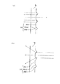
(第1の実施形態)
図1は、本発明の第1の実施形態の光学スケールを製造するための金型の断面図であり、図2は従来例を示す図である。
【0026】
図2のように、光学スケール3のスリット部11を形成する金型部12とシャフト取り付け穴3fを形成する金型部13が可動側の型7と固定側の型8のそれぞれに配置されている場合、可動型7と固定型8の合わせによりスリット部11とシャフト取り付け穴3fの位置関係は変動する。これにより図2の金型構成によって製作された光学スケールを光学式エンコーダに用いた際、その出力信号における累積精度は、ばらつきを大きく持つこととなり、高精度な速度制御や位置決め制御を行うことが困難となる。
【0027】
これに対して、図1に示すようなスリット部11を形成する金型部12とシャフト取り付け穴3fを形成する金型部13の両金型部が固定型8のみに配置されている場合は、これら2つの金型部の位置関係は加工時の嵌合精度に依存するため、安定した同軸度を得ることが可能となる。このことにより、光学スケールの出力信号における累積精度ばらつきを低減させることが可能となり、さらにその累積精度からスリット部11とシャフト取り付け穴3fの偏芯を算出し、その値をもとに偏芯を補正することにより、さらに高精度の出力信号を検出することが可能となる。なお、図1において、10は樹脂材料を金型内に射出するためのゲートであり、9は可動型7と固定型8を分離するパーテーションラインである。
【0028】
次に、図1に示した金型構造によって製作された光学スケールを光学式ロータリーエンコーダに用いた場合の出力信号における累積精度について説明する。
【0029】
図3は光学系の要部斜視図、図4は光学系の要部断面図、図5は光学スケールの説明と、光学スケールの格子部と受光部からの信号の説明のための図、図6は光学スケールの要部断面図である。
【0030】
図中、1は光源であり、例えばLEDや半導体レーザで構成し、波長λ(632.8nm)の可干渉性光束を発している。2はレンズ系であり、球面レンズ又は非球面レンズより成り、光源1からの光束を集光して、後述する光学スケール3に導光している。
【0031】
光源1とレンズ系2は、光照射部LRの一要素を構成している。3は位相差検出機能と振幅型の回折格子機能とを有する光学スケールであり、図3に示すように円板状の基板の表面上に一定周期の複数の放射状格子より成る格子部3dを設けて構成されている。光学スケール3の基板は透光性の光学材料(樹脂材料)より成り、回転体(不図示)の一部に取り付けられており、その回転体と一体的に回転軸3eを中心に矢印6方向に回転する。
【0032】
図5(A),(B)は光学スケール3の格子部3dの詳細図であり、V溝部を構成する2つの傾斜面30b−1,30b−2と1つの平面部30aが所定のピッチPで交互に配列されて格子部3dを形成している。V溝幅は(1/2)Pであり、またV溝を形成する2つの傾斜面30b−1,30b−2は各々(1/4)Pの幅を有し、各々の傾斜面30b−1,30b−2は、平坦部30aに対し各々臨界角以上、本実施形ではθ=45°で傾いている。
【0033】
本実施形態では、光学スケール3の材質をポリカーボネイトとし、射出成形もしくは圧縮成形等の製法によって作成している。この時、光学スケールを成形する金型は、図1のような固定型8と可動型7からなる成形金型であり、光学スケール3のシャフト取り付け穴3fを形成する金型部13とスリット部11を形成する金型部12の両金型部が可動型7もしくは固定型8のどちらか一方に構成され、両金型部の位置関係が高精度に保たれている。
【0034】
図6にその光学スケール3の断面図を示す。この光学スケール3は、モーターのシャフトに組付けるためのボス3gとフランジ3hが一体成形されている。このボス3gの軸中心から図1のようにピンゲート10で樹脂を流入させ、樹脂の流れを軸中心から放射状にすることにより素材内の配向や内部歪みが均一になり高精度の光学スケールを得ている。これは、光学スケール3のV溝の形状を忠実に成形で再現しなければS/Nの良い信号を得ることができないため、V溝の溝方向と平行に樹脂が流れるようにするものである。4は凹面ミラーであり、球面ミラー、楕円ミラー、放物ミラー、非球面ミラー等から成っている。凹面ミラー4は格子部3dのフーリエ変換面に一致している。
【0035】
本実施形態では図3,図4に示すように、レンズ系2で集光され、光学スケール3の第1領域3aに入射した光束が光学スケール3の格子部で回折し、このときn次の回折光(0次と±1次の回折光)が凹面ミラー4の面又はその近傍(凹面ミラー4の瞳位置又はその近傍)に集光するように各要素を設定している。
【0036】
凹面ミラー4の光軸と入射光束の中心光線(主光線)は図4に示すように偏心量Δだけ偏心している。凹面ミラー4は、光学スケール3で回折し、集光してきた収束光束(3つの回折光束)を反射させ、光学スケール3の面上の第2領域3bに3つの回折光に基づく干渉パターン像(像)を再結像させている。このとき光学スケール3が回転方向6に移動すると再結像した像は回転方向6とは反対の方向に移動する。即ち、格子部と干渉パターン像は相対的に光学スケール3の移動量の2倍の値で相対変位する。本実施形態では、これにより光学スケール3に構成されている格子部の2倍の分解能の回転情報を得ている。
【0037】
5は受光部であり、光学スケール3の格子部3dの第2領域3b近傍に形成した干渉パターンと格子部のV溝との位相関係に基づく光束が第2領域3bで幾何学的に屈折され、射出した3つの光束を各々受光するための3つのフォトディテクタ(受光素子)5a,5b,5cを有している。この受光部5からの信号をパルスカウント回路や回転方向の判別回路を有する信号処理回路によって処理し、これより回転情報を得ている。なお、光源1、レンズ系2、そして受光部5は筐体PK内に固定保持されている。
【0038】
次に本実施形態における光学スケール(回転体)3の回転情報の検出方法について説明する。
【0039】
光照射部の一要素であるLED1からの光束をレンズ系2により凹面ミラー面上4の反射面又はその近傍に集光するようにしている。この収束光を図3に示すように光学スケール3の格子部3d上の第1領域3aに入射させる。第1領域3aに入射した収束光のうち図5に示す格子部3dの平面部30aに到達した光線は該平面部30aを通過して凹面ミラー4に進み、その面上に結像する。またV溝を構成する傾斜面30b−1に到達した光線は、傾斜面30b−1の傾斜角が臨界角以上に設定されているため、図に示すように全反射してV溝を構成する他方の傾斜面30b−2に向けられ、傾斜面30b−2においても全反射する。
【0040】
このように最終的に格子部3dの傾斜面30b−1へ到達した光線は、光学スケール3の内部に進入することなく、入射方向に戻されることになる。同様にV溝を構成する他方の傾斜面30b−2に到達した光線も全反射を繰り返して戻される。従って第1領域3aにおいてV溝を形成する2つの傾斜面30b−1,30b−2の範囲に到達する光束は、光学スケール3内に進入することなく反射され、平面部30aに到達した光線のみが光学スケール3を進むことになる。
【0041】
即ち、第1領域3aにおいて、V溝型の格子部3dは透過型の振幅回折格子と同様の光学作用を有する。この第1領域3aの格子部3dで光束は回折され、格子部の作用により0次、±1次、±2次‥‥の回折光が生じ、凹面ミラー4の面上にその回折光が集光する。集光した回折光は、主光線101aに対して偏芯している凹面ミラー4によって反射し、光学スケール3の第2領域3b部で再結像し、光学スケール3の面上に像(放射状の溝の像)を再結像する。
【0042】
ここで第1領域3aと第2領域3bは光学スケール3の面の放射状格子の格子部3dに対して半径方向に異なった(一部が重複していても良い)領域である。このとき、光学スケール3は放射状の格子部3dを有するため、第1領域3aと第2領域3bの格子ピッチが異なる。さらに、第2領域3bの照射領域においても光学スケール3の内周側と外周側のピッチが異なっている。
【0043】
そこで本実施形態では、格子部3d上の第2領域3bに第1領域3aの格子部を拡大投影し、光学スケール3の放射状の格子部3dのピッチと同様の像(反転像)を形成するようにしている。そのために本実施形態では凹面ミラー4を所望の曲率半径Rに設定し、入射光束の主光線に対して偏心配置するとともに入射光軸に対するずれ量Δも最適な値にしている。
【0044】
これによって第1領域3aの格子部の像が凹面ミラー4によって第2領域3b面上に再結像するとき放射状格子の一部のピッチが合致するようにしてS/N比の良い検出信号を得ている。
【0045】
本実施形態では凹面ミラー4で反射し、格子部3dの第2領域3b上に再結像した3つの光束のうち、今度は格子部3dで幾何学的に屈折する光束のみを用いている。
【0046】
第2領域3bにおいて平面部30aに入射した光束は、図5(B)に示すように直線透過し、受光部5の中央部のフォトディテクタ5cに到着する。また、V溝面を形成する2つの傾斜面30b−1及び30b−2に到達した光線は、各々の面に45°の入射角を持って入射するため、それぞれ異なる方向に大きく屈折して受光部5の両側のフォトデイテクタ5a及び5bに到達する。
【0047】
このように第2領域3bにおいて、入射光束に対して異なる方向に傾斜した2つの傾斜面30b−1,30b−2及びV溝の間の平面部30aの合計3種の傾き方向の異なる面により、光束は3つの方向に別れて進み、各々の面に対応した位置に設けられた各フォトディテクタ5a,5b,5cに到達する。即ち第2領域3bにおいてV溝の格子部3dは光波波面分割素子として機能する。
【0048】
即ち第2領域3bの格子部と、その面上に結像した干渉パターン像との位相関係に基づく光束が3方向に偏向され、各フォトディテクタ5a,5b,5cに入射している。
【0049】
ここで光学スケール3が回転すると、各フォトディテクタ5a,5b,5cで検出される光量が変化する。格子部3dの位置と像の位置の相対的変位に応じ、各フォトディテクタに入射する光量バランスが変化し、その結果、光学スケール3が反時計廻りに回転したとすると、図5(C)に示すような光学スケール3の回転に伴う光量変化が得られる。ここで横軸は光学スケール3の回転量、縦軸は受光光量である。
【0050】
信号a,b,cはそれぞれフォトディテクタ5a,5b,5cに対応している。なお、逆に光学スケール3が時計廻りに回転した場合は、信号aはフォトディテクタ5b、信号bはフォトディテクタ5a、信号cはフォトディテクタ5cの出力となる。これらの信号を基に光学スケール3の回転角度や回転量あるいは回転速度や回転加速度等の回転情報を得ている。
【0051】
なお、図5(C)は第2領域3bに形成される像のコントラストが非常に高く理想に近い場合の理論的な光量変化の様子を示している。
【0052】
図7は本光学系における累積精度で、横軸は光学スケール3の回転量、縦軸はスケールピッチの読み取り誤差の累積値である。図7の累積精度において、本実施形態の光学スケールを5個測定した結果、累積精度の個体差が非常に小さく、スリット部とシャフト取り付け穴との位置関係が成形時に保たれていることが分かる。更に光学スケール3内に不均一な樹脂の流れが無くV溝の転写性も良好であるため、光学スケール一周に対する1次の偏芯成分以外の高次成分がほどんど存在していない。
【0053】
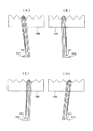
(第2の実施形態)
次に、第2の実施形態について説明する。図8は、第2の実施形態の金型構成を示す図である。
【0054】
図8のようにスリット部11を形成する金型部12とシャフト取り付け穴3fを形成する金型部13の両金型部が可動型7のみに配置されているため、これら2つの金型部の位置関係は加工時の嵌合精度に依存しており、安定した同軸度を得ている。この場合、ゲート10は輪体状に構成されている。効果は、第1の実施形態と同等である。
【0055】
(第3の実施形態)
次に、第3の実施形態について説明する。図9は、第3の実施形態の金型構成を示す図である。
【0056】
図9のようにスリット部11を形成する金型部12とシャフト取り付け穴3fを形成する金型部12が一体で構成されており、その金型部が固定型8に配置されているため、スリット部11とシャフト取り付け穴3fは安定した同軸度を得ている。効果は、第1の実施形態と同等である。
【0057】
(第4の実施形態)
次に、第4の実施形態について説明する。図10は、第4の実施形態の金型構成を示す図である。
【0058】
図10のようにスリット部11を形成する金型部12とシャフト取り付け穴3fを形成する金型部12が一体で構成されており、その金型部が可動型7に配置されているため、スリット部11とシャフト取り付け穴3fは安定した同軸度を得ている。効果は、第1の実施形態と同等である。
【0059】
(第5乃至第8の実施形態)
図11乃至図14の金型構成図は、スケール3がディスク形状の場合であり、効果は第1の実施形態と同等である。
【0060】
(第9乃至第13の実施形態)
図15乃至図19は、スリット部の形状図である。図15乃至図19の形状は、全て波面分割機能を有しており、第1の実施形態と同様に複数の受光素子に波面を分割し、その光強度から移動体の位置もしくは速度を検出する。このようなスリット部をスケール面上に形成させる際、図1、図8乃至図14の金型構成にて製作する。これに対する効果は、第1の実施形態と同等である。
【0061】
以上説明したように、上記の実施形態によれば、光学スケールをプラスチック製とし、さらに光学スケールのシャフト取り付け穴を形成する金型部とスリット部を形成する金型部の両金型部が可動型もしくは固定型のどちらか一方に構成され、シャフト取り付け穴とスリット部の同軸度が安定して得られているため、高精度の移動情報を出力することが可能な光学スケールとその成形に直接使用される成形金型とを提供することができる。
【0062】
(第14の実施形態)
上記の第1乃至第13の実施形態では、光透過型の光学スケール(エンコーダ)について説明したが、この第14の実施形態では、光反射型の光学スケール(エンコーダ)について説明する。
【0063】
図20は、光学式反射型エンコーダスケールのスケール反射部の斜視図である。
【0064】
図中、103は反射部OEが含まれる反射体(反射スケール)である。本実施形態において反射部OEは斜視図のほぼ中央に位置する複数のV字型溝群を指す。103a,103bはV字型溝を構成する2つの傾斜面である。この反射部OEが形成された反射体103の基板は、透過性部材TT1からなり、ポリメチルメタリクレート(PMMA)、ポリカーボネート(PC)、ノルボルネン(PCPD)系の透明耐熱樹脂「アートン」(熱変形温度170℃の耐熱性)等の透過製樹脂からなる。
【0065】
本実施形態の反射体は、2つの反射面103a,103bを所定の角度(85°〜95°)で対向配置したルーフミラーを複数個、一次元方向に配列した反射部(マイクロルーフミラーアレイ)を透明基板(透光性樹脂)の面に設けて構成されている。
【0066】
ここで、ルーフミラー面は、透光性樹脂の内部全反射による反射作用を用いるか、又は金属鏡面反射面を用いる。
【0067】
まず本実施形態の反射体の光学作用を従来の反射体と対比して説明する。
【0068】
図26は従来の反射体203の説明図である。
【0069】
図26は光源201からの発散光束が反射体203の入射面203Fより入射し、平面より成る反射面203Rで反射して、光束の広がり角度が維持されたまま受光部202側へ導かれる様子を示している。
【0070】
図27(A)、(B)、(C)は反射体3に1つのルーフミラーを用いた場合の光路図である。
【0071】
図27は、2つの反射面303a,303bを所定の角度で対向配置したルーフミラーの1個で光束を反射させるように配置した場合を示している。
【0072】
図27(A)では光源1から全方向に反射された光束が先の図26で示したのとほぼ同等の広がり角度をもって受光部302側へ導かれる。
【0073】
2つの反射面303a,303bで分割された光源301からの発散光束は重なり合うことなく受光部2側へ進行する。
【0074】
図27(B),(C)は光源301からの反射された発散光束が2つの光束に分割されることを示している。
【0075】
図27(B),(C)では、光源301から片方に放射された光束がルーフミラーを構成する2つの傾斜303a,303bで分割分離されている。
【0076】
例えば図27(B)では光源301から右側に放射された光束が受光部302側で左方に導光されている。ルーフミラーにより分割、分離後の光束は重なることなく受光部302側へ進んでいる。
【0077】
図28は本実施形態の反射体103の光学作用の説明図である。
【0078】
2つの反射面103a,103bを所定の角度で対向配置したルーフミラーを複数個、一次元方向に配列した反射部OEを透明基板103eの一面に設けている。
【0079】
光源101からの発散光束は反射体103の反射部OEで反射した後、任意の位置(受光部102又はその近傍)で互いに重なっている。
【0080】
光源101からの発散光束は受光部103の面内に略収まり、光源101から広がり角度を持って発光した光束は受光面102に略収まり、受光部102面上の光束の光線密度が上がっている。
【0081】
図29(A)〜(D)は、光源101から種々の方向に発散した光束が反射体103に入射し、複数のルーフミラーによって複数の光束に分割されルーフミラーで反射した後に、各ルーフミラーで反射した光束が任意の位置(受光部102又はその近傍)で互いに重なり合う状態を示している。
【0082】
いずれの場合も反射体103からの反射光は受光部102又はその近傍で光束が互いに重なり合っている。
【0083】
各ルーフミラーの傾斜面ごとの光束が分割分離するが、図29(A)と(D)の反射光束は受光面102上で重なり合い、又、図29(B)と(C)の反射光束は受光面102上の同じ領域で重なり合っている。
【0084】
図30(A),(B)は反射体103の基板となる透過性部材の材質の屈折率の違いによる光線作用の違いを説明するための図である。
【0085】
図30(A)は透過性部材103eの材質の屈折率が1.69の場合、図30(B)は屈折率が1.53の場合である。
【0086】
材質の屈折率が高いと臨界角が小さくなり、全反射するための光線入射角度が緩和される。本実施形態の反射体では、高屈折率の透過性部材を用いており(屈折率1.65以上)これにより光の利用効率を高めている。
【0087】
図31、図32は、反射部を構成するルーフミラーの数による反射光束の集光状態を示した図である。
【0088】
図31(A)〜(C)において、ルーフミラーの数が増すごとに傾斜面1面当りの反射面が光源101を見込む角度:θrは小さくなり、同時に、分割された光束の1光束の光量は減少するが、受光面102へ導かれる反射光束の受光面上の照射領域も小さくなる。
【0089】
ルーフミラーの数が増えることで光量の減少分は打ち消され、トータル光量は変わらず、受光面102への照射面積が小さくなる効果のみが有効となる。
【0090】
図32(A)〜(C)は、同一の発散角度を持って光源101から出射した光束が反射体103に入射して、しかも光源との距離を同一にした時を示している。図32(A)〜(C)において受光面102上へ導かれる光束の光線密度はルーフミラーのピッチが小さくなるほど高くなっている。
【0091】
本実施形態における反射部位は以上の構成を基本としている。
【0092】
図33は、この反射部位を有したロータリスケールを含むロータリエンコーダの構成の概要を示す斜視図である。
【0093】
図34は放射状に配置された反射部位の構成を示す斜視図である。
【0094】
図35、および図36は図34における矢視A、Bから見た図である。
【0095】
次に図20を用いて、本実施形態の反射素子(反射体)の光学作用を説明する。
【0096】
フォトセンサを構成するセンサ光源からの光束(不図示)は、図20の反射体103の下方(V字型溝を設けた面と対向する面)より反射体103に照射され、透光性部材TT1の内部を光束が進行する。そのうち、V字型溝部へ到達した光束は、内部全反射の作用により2回の全反射を繰り返して、再びフォトセンサの光源101側の空間へ戻され、フォトセンサを構成するセンサ受光部へ導かれる。なお、図中、Saは反射体103の変位方向を示している。
【0097】
反射体103の反射部分は、複数の連続したV字型溝よりなり、この複数のV字型溝が連続して配列された、「V字型溝群」OEを一体的な光学エレメントとしての反射部としている。
【0098】
本実施形態において、図中Laは不図示の反射式エンコーダにおける光源の発光面に立てた法線で、この法線Laは光源から反射体103に照射される光束の主光線と一致し、その主光線と反射スケール(反射体103)はほぼ垂直に交わっている。
【0099】
図21は、第14の実施形態の反射式リニアエンコーダ用スケールとしての反射体103を上面(Z軸方向)から見た図である。
【0100】
本実施形態の反射素子OEは、変位測定方向Saに沿って図中、P1で示される間隔(ピッチ)で配列されている。このピッチP1は、反射式エンコーダ用スケールのスケールピッチに相当し、センサによる変位測定の際の測定分解能を決定する。
【0101】
さらに図21中のA−A断面図、B−B断面図にてこの反射体103の特徴を説明する。
【0102】
図22、図23は、それぞれ図21のA−A断面およびB−B断面を表している。以下、図22、図23での図中記号を説明する。
【0103】
103a,103b:V字型溝OEを構成する2つの傾斜面
Ra:2つの傾斜面103a(103a1,103a2…),103b(103b1,103b2…)のなす角度(V字型溝の開き角)
Pm:V字型溝の配列ピッチ
d:V字型の溝深さ
P1:反射素子OEの配列周期(=エンコーダスケールピッチ)
上記の形状パラメータに対して、本実施形態での具体的な設計値例としては、
P1≒169μm
Pm≒100〜200μm
Ra≒95°
Wrma≒85μm
d2≒Pm/2+10μm
d≒Pm/2 (50〜100μm)
また、図22中、nは、光源からの主光線Laと平行な直線をあらわし、本実施形態ではV字型溝のなす角を2等分する。
【0104】
図23において、面103cは平面平坦部で、V字型溝群の間に存在しており、この部分への裏面TT1bから照射された光束は、全反射せず透過して、エンコーダ側の受光素子部へ入射しない。
【0105】
図23において、面103cと面103cとの間の凹部の斜面310dと、面103cの法線103eとのなす角度Rbは射出成形技術で反射スケール103を製造する際に必要な金型の抜き勾配としての角度を設けており、具体的にはRb≒3°〜5°程度である。
【0106】
以上、第14及び15の実施形態では、複数の連続したV字型溝群による透光性部材の内部全反射の作用を利用している。このため反射体103は、その基板の表面にアルミ反射膜などを施さずに、実質的な光束の反射機能を果たしている。
【0107】
本実施形態の反射体103は内部全反射の作用を利用した透光性部材である。
Ra=90度の設定でしかもピッチPmを問題ない寸法に設定した場合に、実現可能なフォトセンサ側の構成例として、図24の構成が適用できる。
【0108】
図24において、反射スケール103は透光性部材からなり角度Ra=90度の設定である。
【0109】
この場合には、受光素子102のシリコンフォトダイオードのチップ上にLED101のチップを載せて実装し、上述の問題を回避することが可能である。実装密度が高い点では好ましい構成ともいえるがLED101の発熱を考慮する必要がある。
【0110】
実装面から考えると角度オフセットを与え(90度よりも大きな角度に設定し)図25のように同一の実装面にシリコンフォトダイオード102と、LEDチップ101を並べて実装するのが好ましい。
【0111】
そこで有効な手段としては、この角度Raを90度より大きい角度に設定することが良い。
【0112】
これまでスケールの光学的な作用について説明してきたが、このような溝形状を施すことにより、光学式反射型エンコーダスケールとしての機能が実現可能となる。
【0113】
次に、このスケールを高精度に成形するための成形金型の構造、および、このスケールをエンコーダユニットとして被回転角度検出軸に組み付けた場合の検出ヘッドとの関係について説明する。
【0114】
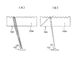
図37は、本実施形態のスケールを成形するための金型構造を示す図である。
【0115】
軸取付け部103fと光線反射機能部(V字型溝)111を同一の金型部材から形成し、可動側型112と、1点ピンディスクゲート110を有する固定側型107とを用いて、本実施形態のスケール103は成形される。このことにより、溶融樹脂はセンターに位置するピンゲートを中心に放射方向に均一に流動し、応力分布や寸法精度の面で周方向において均一な特性、精度が得られる。さらに、反射部位と軸嵌合部が同一駒型に配置されることで、得られる成形品形状は図38のような形状となる。そのため、モータ等の回転軸に装着する場合に、図39に示したように、反射部が軸受け近傍に位置することとなり、軸受けガタ、遊びに起因する軸の旋回(振れまわり)が発生した場合においても、偏芯誤差及び反射面の軸方向の上下動を小さく抑えることが可能となるとともに、検出ヘッドの配置もスケールの嵌合長を確保するための凸形状部の高さhの寸法内に収めることが可能となり、ユニットの薄型化への効果が大きい。
【0116】
図40は他の実施例のスケール形状を示す図で、図37と同様の金型構造をとるが、図41に示したカッティングラインCLにて切断して、貫通穴としている。この場合には、エンコーダユニットとしては、図42のように、スケール103およびヘッドが配置される。先の実施例に対して、ユニットとして占有する体積は膨らむが、検知ヘッド101,102と軸受け部材とが同一部材上に配置されヘッド101,102、スケール103間の位置決め精度の面で有利なレイアウトが実現可能となる。この場合においても先の例と同様に、軸嵌合部103fと反射部111が同一の金型駒で成形されるため、部品単体での反射部パターンセンターと軸嵌合穴との関係は高精度に保たれる。
【0117】
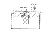
図43は、先の例と異なり、ピンディスクゲート10のゲート位置をディスクのセンターにレイアウトせずに、たとえば図のようなハブ部位端部に配置している。このようにすることで先の実施例での軸の貫通穴をあけるための2次加工をなくすことが可能で成形品形状としては、図44のように軸保持部として貫通した穴形状103fが得られる。ここでも先の例と同様に、軸嵌合部103fと反射部111が同一の金型駒で成形されるため、部品単体での反射部パターンセンターと軸嵌合穴との関係は高精度に保たれる。
【0118】
図45は、さらに先の例と異なり、回転角度検出軸との結合部分が凸形状、軸側が凹形状として結合された構成となっている。ピンディスクゲートのゲート位置は図の上側のディスクのセンターにレイアウトさせている(不図示)。
【0119】
ここでも先の例と同様に、軸嵌合部103fと反射部111が同一の金型駒で成形されるため、部品単体での反射部パターンセンターと軸嵌合穴との関係は高精度に保たれる。
【0120】
また、ヘッド、スケールの配置に関しても最小のスペースに収まっており薄型化の効果が大きい。
【0121】
図46もほぼ同様の構成であるが先程のスケールの軸結合部凸形状部分が回転軸と結合せず、ベアリングの内輪に結合された構成となっている。
【0122】
この場合の効果も図45と同様である。
【0123】
以上のように、第14の実施形態によれば、測定、観測対象となる反射体に設ける反射素子を適切に構成することにより、フォトセンサにレンズを用いなくても高い光伝達効率が得られ、又、反射体とフォトセンサ間の相対的な位置ずれに対しても感度の鈍い特性となり、反射体の有無や移動状態を高精度に検出することができる反射体及びそれを用いたエンコーダ等の光学装置を達成することができる。
【0124】
また、反射体を光学センサ用の標識部材、光学スケールとして用いることで、発光、受光間で高い光伝達効率が得られ、また、反射体、センサ間の相対的な位置ずれに対しても感度の鈍い特性にすることができ、レンズが不要なためセンサの小型化、薄型化が可能となる。又、反射膜等を施すことなくインジェクションモールドやプレス技術で製造可能なため、加工コストもかからずローコスト化に有効となる。
【0125】
【発明の効果】
以上説明したように、本発明によれば、製作が容易でありながら、高精度な移動信号の出力を可能とする光学スケールを提供することができる。
【図面の簡単な説明】
【図1】本発明の第1の実施形態の光学スケールを製造するための金型の断面図である。
【図2】従来の金型構造を示す断面図である。
【図3】ロータリーエンコーダの光学系の要部斜視図である。
【図4】ロータリーエンコーダの光学系の要部断面図である。
【図5】光学スケールの説明と、光学スケールの格子部と受光部からの信号の説明のための図である。
【図6】光学スケールの断面図である。
【図7】ロータリーエンコーダの累積精度を示す図である。
【図8】本発明の第2の実施形態の金型の断面図である。
【図9】本発明の第3の実施形態の金型の断面図である。
【図10】本発明の第4の実施形態の金型の断面図である。
【図11】本発明の第5の実施形態の金型の断面図である。
【図12】本発明の第6の実施形態の金型の断面図である。
【図13】本発明の第7の実施形態の金型の断面図である。
【図14】本発明の第8の実施形態の金型の断面図である。
【図15】本発明の第9の実施形態のスケールの断面図である。
【図16】本発明の第10の実施形態のスケールの断面図である。
【図17】本発明の第11の実施形態のスケールの断面図である。
【図18】本発明の第12の実施形態のスケールの断面図である。
【図19】本発明の第13の実施形態のスケールの断面図である。
【図20】1次元収束性反射素子で、リニアエンコーダ用スケールとして用いたときの斜視図である。
【図21】図20のリニアエンコーダ用スケールを光源光軸方向からみた上面図である。
【図22】図20のリニアエンコーダ用スケールのY−Z断面図(図21の矢視A−A図)である。
【図23】図20のリニアエンコーダ用スケールのX−Z断面図(図21の矢視B−B図)である。
【図24】第14の実施形態の反射スケールの反射光路を表すオフセットなしでの図である。
【図25】第14の実施形態の反射スケールの反射光路を表すオフセットありでの図である。
【図26】従来の反射体の光路を示す概略図である。
【図27】2つのV溝を有する反射体の光路を示す概略図である。
【図28】第14の実施形態の反射体の光路を示す概略図である。
【図29】第14の実施形態の反射体の光路を示す概略図である。
【図30】第14の実施形態の反射体の光路を示す概略図である。
【図31】第14の実施形態の反射体の光路を示す概略図である。
【図32】第14の実施形態の反射体の光路を示す概略図である。
【図33】第14の実施形態のロータリエンコーダの構成を示す概略図である。
【図34】第14の実施形態のロータリエンコーダスケールの構成を示す概略図である。
【図35】第14の実施形態の反射体の光路を示す概略図である。
【図36】第14の実施形態の反射体の光路を示す概略図である。
【図37】第14の実施形態のスケール用金型断面図である。
【図38】第14の実施形態のロータリエンコーダスケールの製品断面図である。
【図39】第14の実施形態のロータリエンコーダの構成を示す概略図である。
【図40】第14の実施形態の他の例のスケール用金型断面図である。
【図41】第14の実施形態の他の例のロータリエンコーダスケールの製品断面図である。
【図42】第14の実施形態の他の例のロータリエンコーダの構成を示す概略図である。
【図43】第14の実施形態のさらに他の例のスケール用金型断面図である。
【図44】第14の実施形態のさらに他の例のロータリエンコーダスケールの製品断面図である。
【図45】第14の実施形態のさらに他の例のロータリエンコーダの構成を示す概略図である。
【図46】第14の実施形態のさらに他の例のロータリエンコーダの構成を示す概略図である。
【符号の説明】
1 光照射部
2 レンズ
3 光学スケール
3a 第1領域
3b 第2領域
3d 格子部
3e 回転中心
4 凹面ミラー
5 受光素子
5a,5b,4c 受光素子
6 回転方向
7 可動型
8 固定型
9 パーテーションライン
10 ゲート
11 スリット部
12 スリット駒
13 スケール勘合穴用ピン
14 ロータリースケール
30a 平坦部
30b−1,30b−2 V溝
103 信号処理回路
a 受光素子4aで得られる信号
b 受光素子4aで得られる信号
c 受光素子4aで得られる信号
101 光源
102 受光素子
103 反射スケール
103a,103b V溝を形成する斜面
103c1,103c2 平坦面
P1 スケールピッチ
Pm V溝のピッチ
Ra V溝の角度
d V溝の深さ
L 光源ポイント
P 受光ポイント
La 光源から立てた法線
Sa センサと反射体の相対変位方向
Wrma V溝群の相対変位方向(X軸方向)の幅[0001]
BACKGROUND OF THE INVENTION
The present invention relates to an optical encoder that detects movement information with high accuracy, an optical scale used therefor, and a molding die for molding the optical scale.
[0002]
[Prior art]
Conventionally known methods for detecting the position and speed of a moving body are roughly classified into a method using a magnetic encoder and a method using an optical encoder. Of these, the optical encoder mainly includes a light projecting unit, a light receiving unit, and a scale. A thin SUS (stainless steel) material is used for the scale, and it is generally manufactured by precision press punching or etching, and the one described in Japanese Utility Model Publication No. 63-33409 corresponds to this.
[0003]
[Problems to be solved by the invention]
However, the scale manufactured by the above-described prior art is composed of a scale and a hub in order to guarantee the coaxiality of the scale slit portion and the hub portion because the hub portion necessary for fixing to the motor shaft is composed of separate parts. There is a problem in that it is necessary to make adjustments when bonding, and it takes time to manufacture.
[0004]
Conventionally, as a scale for an optical rotary encoder, a metal scale having a thickness of about 0.05 mm to 0.2 mm is etched using a metal scale having a slit portion or a photograph having a thickness of about 0.2 mm. A film scale with slits formed on the plate-making film by means of photographic development or other means for light transmission and light absorption. For high-precision scales used in fields where accuracy is required, a metal thin film is deposited on a glass substrate. A glass scale having a slit portion formed by a technique such as photoetching is used.
[0005]
However, since any of the above-mentioned scales is indirectly coupled to the rotating shaft via the hub member, the eccentric accuracy between the center of the slit formed in the scale and the rotating shaft is high. It was difficult to fix while maintaining a high level, requiring a high degree of adjustment. Similarly, because of the above-described configuration, it is difficult to maintain the squareness with the rotation axis with high accuracy with respect to the scale runout due to rotation. Furthermore, since the thickness of the scale is 0.2 mm or less in the metal scale or the film scale, the flatness is inferior, the fluctuation of the surface (flapping) is large, and the angle detection accuracy is deteriorated. A glass scale with a relatively high degree of flatness is relatively easy to increase the squareness accuracy, but has the disadvantage of being vulnerable to impact and expensive.
[0006]
In addition, the measure that attempts to avoid such a factor of accuracy deterioration results in a problem that the encoder unit is reduced in size and cost. For example, with regard to the dimension of the encoder in the thickness direction (axial thrust direction), it is required to increase the dimension of the scale mounting hub in order to minimize surface deflection, and the overall dimension of the encoder unit in the thrust direction increases. As a result, it is difficult to reduce the thickness of the product, and the assembly is performed while maintaining the coaxiality and squareness with high accuracy, so that an advanced adjustment process is required and the cost is increased.
[0007]
Accordingly, the present invention has been made in view of the above-described problems, and an object of the present invention is to provide an optical scale capable of outputting a highly accurate movement signal while being easy to manufacture, and a molding die and an optical type thereof. It is to provide an encoder.
[0008]
[Means for Solving the Problems]
In order to solve the above-mentioned problems and achieve the object, it relates to the present invention.The optical scale is an optical scale formed by a fixed mold and a movable mold. The optical scale reflects a light beam emitted from a light emitting element and holds a shaft with a reflecting portion for guiding the reflected light beam to a light receiving means. A shaft holding portion for rotating, the reflecting portion is disposed on the same surface side as the shaft holding portion, the shaft holding portion is integrally formed by one of the fixed mold and the movable mold, and the other It has an injection gate at a position corresponding to the central portion of the mold scale on the surface side, and is molded by injecting a transparent resin from the injection gate.
[0009]
Also related to this inventionIn the optical scale, the shaft holding portion has a bottomed concave shape portion to be attached to the shaft for rotating the optical scale, and the injection gate is provided on the opposite surface of the bottomed shape portion. And
[0010]
Also,An optical encoder according to the present invention includes a light emitting element and a light receiving element, reflects a light beam projected from the light emitting element by the optical scale, and changes a light beam received by the light receiving element. Based on this, the amount of movement of the scale is detected.
[0024]
DETAILED DESCRIPTION OF THE INVENTION
DESCRIPTION OF EXEMPLARY EMBODIMENTS Hereinafter, preferred embodiments of the invention will be described in detail with reference to the accompanying drawings.
[0025]
(First embodiment)
FIG. 1 is a sectional view of a mold for manufacturing an optical scale according to a first embodiment of the present invention, and FIG. 2 is a view showing a conventional example.
[0026]
As shown in FIG. 2, a
[0027]
On the other hand, when both mold parts of the
[0028]
Next, the accumulation accuracy in the output signal when the optical scale manufactured by the mold structure shown in FIG. 1 is used for the optical rotary encoder will be described.
[0029]
3 is a perspective view of the main part of the optical system, FIG. 4 is a sectional view of the main part of the optical system, FIG. 5 is a diagram for explaining the optical scale, and signals from the grating part and the light receiving part of the optical scale. 6 is a cross-sectional view of the main part of the optical scale.
[0030]
In the figure,
[0031]
The
[0032]
5A and 5B are detailed views of the
[0033]
In this embodiment, the
[0034]
FIG. 6 shows a cross-sectional view of the
[0035]
In this embodiment, as shown in FIGS. 3 and 4, the light beam collected by the
[0036]
The optical axis of the concave mirror 4 and the central ray (principal ray) of the incident light beam are decentered by an eccentric amount Δ as shown in FIG. The concave mirror 4 reflects the converged light beam (three diffracted light beams) that is diffracted and collected by the
[0037]
[0038]
Next, a method for detecting rotation information of the optical scale (rotating body) 3 in the present embodiment will be described.
[0039]
The light beam from the
[0040]
Thus, the light beam finally reaching the
[0041]
That is, in the
[0042]
Here, the
[0043]
Therefore, in the present embodiment, the lattice portion of the
[0044]
As a result, when the image of the grating portion of the
[0045]
In the present embodiment, among the three light beams reflected by the concave mirror 4 and re-imaged on the
[0046]
The light beam incident on the
[0047]
As described above, in the
[0048]
That is, the light beam based on the phase relationship between the grating portion of the
[0049]
Here, when the
[0050]
Signals a, b, and c correspond to the
[0051]
FIG. 5C shows a theoretical change in the amount of light when the contrast of the image formed in the
[0052]
FIG. 7 shows the accumulative accuracy in this optical system. The horizontal axis represents the rotation amount of the
[0053]
(Second Embodiment)
Next, a second embodiment will be described. FIG. 8 is a diagram illustrating a mold configuration according to the second embodiment.
[0054]
As shown in FIG. 8, since both mold parts of the
[0055]
(Third embodiment)
Next, a third embodiment will be described. FIG. 9 is a diagram illustrating a mold configuration according to the third embodiment.
[0056]
Since the
[0057]
(Fourth embodiment)
Next, a fourth embodiment will be described. FIG. 10 is a diagram illustrating a mold configuration according to the fourth embodiment.
[0058]
Since the
[0059]
(Fifth to eighth embodiments)
The mold configuration diagrams of FIGS. 11 to 14 show a case where the
[0060]
(Ninth to 13th embodiments)
15 to 19 are shape diagrams of the slit portion. The shapes shown in FIGS. 15 to 19 all have a wavefront dividing function, and the wavefront is divided into a plurality of light receiving elements as in the first embodiment, and the position or velocity of the moving body is detected from the light intensity. . When such a slit portion is formed on the scale surface, it is manufactured with the mold configuration shown in FIGS. 1 and 8 to 14. The effect for this is equivalent to that of the first embodiment.
[0061]
As described above, according to the above embodiment, the optical scale is made of plastic, and both the mold part for forming the shaft mounting hole of the optical scale and the mold part for forming the slit part are movable. It is configured as either a mold or a fixed mold, and the coaxiality of the shaft mounting hole and the slit part is stably obtained. It is possible to provide a molding die to be used.
[0062]
(Fourteenth embodiment)
In the first to thirteenth embodiments, the light transmission type optical scale (encoder) has been described. In the fourteenth embodiment, a light reflection type optical scale (encoder) will be described.
[0063]
FIG. 20 is a perspective view of the scale reflecting portion of the optical reflective encoder scale.
[0064]
In the figure,
[0065]
The reflector of this embodiment is a reflector (micro roof mirror array) in which a plurality of roof mirrors in which two reflecting
[0066]
Here, the roof mirror surface uses a reflection action by total internal reflection of the translucent resin, or a metal mirror reflection surface.
[0067]
First, the optical action of the reflector of this embodiment will be described in comparison with a conventional reflector.
[0068]
FIG. 26 is an explanatory diagram of a
[0069]
In FIG. 26, the divergent light beam from the
[0070]
FIGS. 27A, 27B, and 27C are optical path diagrams when one roof mirror is used for the
[0071]
FIG. 27 shows a case where a light beam is reflected by one roof mirror in which two reflecting
[0072]
In FIG. 27A, the light beam reflected from the
[0073]
The divergent light beams from the
[0074]
27B and 27C show that the divergent light beam reflected from the
[0075]
In FIGS. 27B and 27C, a light beam emitted from one side of the
[0076]
For example, in FIG. 27B, a light beam emitted to the right side from the
[0077]
FIG. 28 is an explanatory diagram of the optical action of the
[0078]
A reflecting portion OE in which a plurality of roof mirrors each having two reflecting
[0079]
The divergent light beams from the
[0080]
The divergent light beam from the
[0081]
29A to 29D show a case where a light beam diverged in various directions from the
[0082]
In either case, the light beams reflected from the
[0083]
The light flux for each inclined surface of each roof mirror is divided and separated, but the reflected light fluxes of FIGS. 29A and 29D overlap on the
[0084]
FIGS. 30A and 30B are diagrams for explaining the difference in the light beam action due to the difference in the refractive index of the material of the transmissive member that becomes the substrate of the
[0085]
30A shows the case where the refractive index of the material of the
[0086]
If the refractive index of the material is high, the critical angle becomes small, and the light incident angle for total reflection is relaxed. In the reflector according to the present embodiment, a transparent member having a high refractive index is used (refractive index of 1.65 or more), thereby increasing the light utilization efficiency.
[0087]
FIG. 31 and FIG. 32 are diagrams showing the state of condensing reflected light flux depending on the number of roof mirrors constituting the reflecting portion.
[0088]
31A to 31C, as the number of roof mirrors increases, the angle at which the reflection surface per inclined surface looks at the light source 101: θr decreases, and at the same time, the amount of light of one of the divided light beams. However, the irradiation area on the light receiving surface of the reflected light beam guided to the
[0089]
As the number of roof mirrors increases, the decrease in light quantity is canceled out, the total light quantity does not change, and only the effect of reducing the irradiation area on the
[0090]
FIGS. 32A to 32C show a time when light beams emitted from the
[0091]
The reflection site in the present embodiment is based on the above configuration.
[0092]
FIG. 33 is a perspective view showing an outline of a configuration of a rotary encoder including a rotary scale having the reflection portion.
[0093]
FIG. 34 is a perspective view showing the configuration of the reflecting portions arranged radially.
[0094]
35 and 36 are views seen from the arrows A and B in FIG.
[0095]
Next, the optical action of the reflective element (reflector) of this embodiment will be described with reference to FIG.
[0096]
A light beam (not shown) from the sensor light source constituting the photosensor is irradiated onto the
[0097]
The reflective portion of the
[0098]
In the present embodiment, La in the figure is a normal line standing on the light emitting surface of the light source in a reflection encoder (not shown), and this normal line La coincides with the principal ray of the light beam emitted from the light source to the
[0099]
FIG. 21 is a view of the
[0100]
The reflective elements OE of the present embodiment are arranged at intervals (pitch) indicated by P1 in the drawing along the displacement measuring direction Sa. The pitch P1 corresponds to the scale pitch of the reflective encoder scale, and determines the measurement resolution when measuring displacement by the sensor.
[0101]
Further, the characteristics of the
[0102]
22 and 23 show the AA cross section and the BB cross section of FIG. 21, respectively. Hereinafter, symbols in FIGS. 22 and 23 will be described.
[0103]
103a, 103b: Two inclined surfaces constituting the V-shaped groove OE
Ra: angle formed by two
Pm: V-shaped groove arrangement pitch
d: V-shaped groove depth
P1: Arrangement period of reflection elements OE (= encoder scale pitch)
As an example of specific design values in the present embodiment for the above shape parameters,
P1 ≒ 169μm
Pm≈100 to 200 μm
Ra ≒ 95 °
Wrma ≒ 85μm
d2≈Pm / 2 + 10 μm
d≈Pm / 2 (50-100 μm)
In FIG. 22, n represents a straight line parallel to the principal ray La from the light source, and in this embodiment, the angle formed by the V-shaped groove is divided into two equal parts.
[0104]
In FIG. 23, a
[0105]
In FIG. 23, the angle Rb formed by the inclined surface 310d of the recess between the
[0106]
As described above, in the fourteenth and fifteenth embodiments, the action of total internal reflection of a translucent member by a plurality of continuous V-shaped groove groups is used. For this reason, the
[0107]
The
When Ra = 90 degrees is set and the pitch Pm is set to a dimension that does not cause a problem, the configuration in FIG. 24 can be applied as a configuration example on the photosensor side that can be realized.
[0108]
In FIG. 24, the
[0109]
In this case, the above-mentioned problem can be avoided by mounting the
[0110]
Considering the mounting surface, it is preferable to provide an angle offset (set an angle larger than 90 degrees) and mount the
[0111]
Therefore, as an effective means, it is preferable to set the angle Ra to an angle larger than 90 degrees.
[0112]
The optical action of the scale has been described so far, but by providing such a groove shape, a function as an optical reflective encoder scale can be realized.
[0113]
Next, the structure of a molding die for molding the scale with high accuracy and the relationship with the detection head when the scale is assembled as an encoder unit on the rotation angle detection shaft will be described.
[0114]
FIG. 37 is a view showing a mold structure for molding the scale according to the present embodiment.
[0115]
The
[0116]
FIG. 40 is a diagram showing a scale shape of another embodiment, which has a mold structure similar to that of FIG. 37, but is cut by a cutting line CL shown in FIG. 41 to form a through hole. In this case, as an encoder unit, a
[0117]
In FIG. 43, unlike the previous example, the gate position of the
[0118]
FIG. 45 is different from the previous example in that the coupling portion with the rotation angle detection shaft is coupled in a convex shape and the shaft side is coupled in a concave shape. The gate position of the pin disk gate is laid out at the center of the disk on the upper side of the figure (not shown).
[0119]
Here, as in the previous example, since the shaft
[0120]
Also, the arrangement of the head and scale is within the minimum space, and the effect of thinning is great.
[0121]
FIG. 46 also has a substantially similar configuration, except that the convex portion of the shaft coupling portion of the previous scale is not coupled to the rotating shaft but is coupled to the inner ring of the bearing.
[0122]
The effect in this case is the same as in FIG.
[0123]
As described above, according to the fourteenth embodiment, a high light transmission efficiency can be obtained without using a lens in the photosensor by appropriately configuring the reflective element provided on the reflector to be measured and observed. In addition, the reflector has a low sensitivity to the relative displacement between the reflector and the photosensor, and the reflector that can detect the presence / absence and the moving state of the reflector with high accuracy, and the encoder using the reflector, etc. The optical device can be achieved.
[0124]
In addition, by using a reflector as a labeling member for an optical sensor and an optical scale, high light transmission efficiency can be obtained between light emission and light reception, and sensitivity to relative positional deviation between the reflector and sensor is also obtained. Therefore, the sensor can be made smaller and thinner because no lens is required. In addition, since it can be manufactured by injection molding or pressing technology without applying a reflective film or the like, it is effective in reducing costs without incurring processing costs.
[0125]
【The invention's effect】
As described above, according to the present invention, it is possible to provide an optical scale that allows easy output of a movement signal while being easy to manufacture.
[Brief description of the drawings]
FIG. 1 is a sectional view of a mold for manufacturing an optical scale according to a first embodiment of the present invention.
FIG. 2 is a cross-sectional view showing a conventional mold structure.
FIG. 3 is a perspective view of an essential part of an optical system of a rotary encoder.
FIG. 4 is a cross-sectional view of a main part of an optical system of a rotary encoder.
FIG. 5 is a diagram for explaining an optical scale and signals from a grating part and a light receiving part of the optical scale.
FIG. 6 is a cross-sectional view of an optical scale.
FIG. 7 is a diagram illustrating cumulative accuracy of a rotary encoder.
FIG. 8 is a cross-sectional view of a mold according to a second embodiment of the present invention.
FIG. 9 is a cross-sectional view of a mold according to a third embodiment of the present invention.
FIG. 10 is a sectional view of a mold according to a fourth embodiment of the present invention.
FIG. 11 is a sectional view of a mold according to a fifth embodiment of the present invention.
FIG. 12 is a sectional view of a mold according to a sixth embodiment of the present invention.
FIG. 13 is a sectional view of a mold according to a seventh embodiment of the present invention.
FIG. 14 is a sectional view of a mold according to an eighth embodiment of the present invention.
FIG. 15 is a sectional view of a scale according to a ninth embodiment of the present invention.
FIG. 16 is a cross-sectional view of a scale according to a tenth embodiment of the present invention.
FIG. 17 is a cross-sectional view of a scale according to an eleventh embodiment of the present invention.
FIG. 18 is a cross-sectional view of a scale according to a twelfth embodiment of the present invention.
FIG. 19 is a cross-sectional view of a scale according to a thirteenth embodiment of the present invention.
FIG. 20 is a perspective view of a one-dimensional convergent reflecting element when used as a linear encoder scale.
21 is a top view of the linear encoder scale of FIG. 20 as viewed from the direction of the light source optical axis.
22 is a cross-sectional view taken along the line YZ of the linear encoder scale of FIG. 20 (a view taken along the line AA in FIG. 21).
23 is an XZ sectional view of the linear encoder scale of FIG.
FIG. 24 is a diagram without an offset representing a reflected light path of a reflection scale according to a fourteenth embodiment.
FIG. 25 is a diagram with an offset representing a reflected optical path of a reflection scale according to a fourteenth embodiment.
FIG. 26 is a schematic view showing an optical path of a conventional reflector.
FIG. 27 is a schematic view showing an optical path of a reflector having two V grooves.
FIG. 28 is a schematic view showing an optical path of a reflector according to a fourteenth embodiment.
FIG. 29 is a schematic view showing an optical path of a reflector according to a fourteenth embodiment.
30 is a schematic view showing an optical path of a reflector according to a fourteenth embodiment. FIG.
FIG. 31 is a schematic view showing an optical path of a reflector according to a fourteenth embodiment.
FIG. 32 is a schematic view showing an optical path of a reflector according to a fourteenth embodiment.
FIG. 33 is a schematic diagram showing the configuration of a rotary encoder of a fourteenth embodiment.
FIG. 34 is a schematic diagram showing the configuration of a rotary encoder scale according to a fourteenth embodiment.
FIG. 35 is a schematic view showing an optical path of a reflector according to a fourteenth embodiment.
FIG. 36 is a schematic view showing an optical path of a reflector according to a fourteenth embodiment.
FIG. 37 is a sectional view of a scale mold according to a fourteenth embodiment.
FIG. 38 is a product sectional view of a rotary encoder scale according to a fourteenth embodiment.
FIG. 39 is a schematic diagram showing the configuration of a rotary encoder according to a fourteenth embodiment.
FIG. 40 is a sectional view of a scale mold according to another example of the fourteenth embodiment.
FIG. 41 is a product sectional view of a rotary encoder scale according to another example of the fourteenth embodiment.
FIG. 42 is a schematic diagram showing the configuration of another example of a rotary encoder according to the fourteenth embodiment.
FIG. 43 is a sectional view of a scale mold according to still another example of the fourteenth embodiment.
FIG. 44 is a product sectional view of still another example of a rotary encoder scale according to the fourteenth embodiment.
FIG. 45 is a schematic diagram showing the configuration of a rotary encoder of still another example of the fourteenth embodiment.
FIG. 46 is a schematic diagram showing the configuration of a rotary encoder of still another example of the fourteenth embodiment.
[Explanation of symbols]
1 Light irradiation part
2 Lens
3 Optical scale
3a 1st area
3b 2nd area
3d lattice part
3e Center of rotation
4 Concave mirror
5 Light receiving element
5a, 5b, 4c Light receiving element
6 Direction of rotation
7 Movable type
8 Fixed type
9 Partition line
10 Gate
11 Slit
12 Slit pieces
13 Scale mating hole pin
14 Rotary scale
30a Flat part
30b-1, 30b-2 V-groove
103 Signal processing circuit
a Signal obtained by the
b Signal obtained by the
c Signal obtained by the
101 Light source
102 Light receiving element
103 reflection scale
103a, 103b slopes forming V-grooves
103c1, 103c2 flat surface
P1 scale pitch
Pm V groove pitch
Ra V groove angle
d V-groove depth
L Light source point
P Light receiving point
Normal line from La light source
Relative displacement direction of Sa sensor and reflector
Width of relative displacement direction (X axis direction) of Wrma V groove group
Claims (3)
発光素子から発光される光束を反射し、反射光束を受光手段に導くための反射部と、A reflecting portion for reflecting the light beam emitted from the light emitting element and guiding the reflected light beam to the light receiving means;
軸を保持し、スケールを回転させるための軸保持部と、を有し、A shaft holding portion for holding the shaft and rotating the scale,
前記反射部は前記軸保持部と同一面側に配置され、前記軸保持部は前記固定型または可動型の一方により一体的に成形され、他方面側に型のスケールの中央部に対応する位置に注入ゲートを有し、透明樹脂を前記注入ゲートから注入することにより成形されることを特徴とする光学スケール。The reflecting portion is arranged on the same surface side as the shaft holding portion, the shaft holding portion is integrally formed by one of the fixed mold or the movable mold, and the other surface side corresponds to the center portion of the mold scale. An optical scale having an injection gate formed by injecting a transparent resin from the injection gate.
受光素子とを有し、A light receiving element,
前記発光素子から投光された光束を請求項1または2に記載の光学スケールにて反射させ、前記受光素子にて受光した光束の変化に基いて前記スケールの移動量を検出することを特徴とする光学式エンコーダ。The light beam projected from the light emitting element is reflected by the optical scale according to claim 1 or 2, and the amount of movement of the scale is detected based on a change in the light beam received by the light receiving element. An optical encoder.
Priority Applications (2)
| Application Number | Priority Date | Filing Date | Title |
|---|---|---|---|
| JP2001104997A JP4726168B2 (en) | 2000-04-17 | 2001-04-03 | Optical scale and optical encoder |
| US09/832,116 US6891150B2 (en) | 2000-04-17 | 2001-04-11 | Optical scale formed from mold having fixed and movable platens |
Applications Claiming Priority (4)
| Application Number | Priority Date | Filing Date | Title |
|---|---|---|---|
| JP2000115514 | 2000-04-17 | ||
| JP2000-115514 | 2000-04-17 | ||
| JP2000115514 | 2000-04-17 | ||
| JP2001104997A JP4726168B2 (en) | 2000-04-17 | 2001-04-03 | Optical scale and optical encoder |
Publications (3)
| Publication Number | Publication Date |
|---|---|
| JP2002005694A JP2002005694A (en) | 2002-01-09 |
| JP2002005694A5 JP2002005694A5 (en) | 2008-05-15 |
| JP4726168B2 true JP4726168B2 (en) | 2011-07-20 |
Family
ID=26590247
Family Applications (1)
| Application Number | Title | Priority Date | Filing Date |
|---|---|---|---|
| JP2001104997A Expired - Fee Related JP4726168B2 (en) | 2000-04-17 | 2001-04-03 | Optical scale and optical encoder |
Country Status (2)
| Country | Link |
|---|---|
| US (1) | US6891150B2 (en) |
| JP (1) | JP4726168B2 (en) |
Families Citing this family (16)
| Publication number | Priority date | Publication date | Assignee | Title |
|---|---|---|---|---|
| JP4280447B2 (en) * | 2001-02-20 | 2009-06-17 | キヤノン株式会社 | Reflection scale and displacement detection device using the same |
| JP4208483B2 (en) * | 2002-05-21 | 2009-01-14 | キヤノン株式会社 | Optical encoder |
| US6972402B2 (en) * | 2002-06-03 | 2005-12-06 | Mitsubishi Denki Kabushiki Kaisha | Photoelectric rotary encoder |
| JP2004340929A (en) * | 2003-04-21 | 2004-12-02 | Mitsubishi Electric Corp | Optical rotary encoder |
| DE102004019907A1 (en) * | 2003-04-25 | 2005-01-13 | Dr. Johannes Heidenhain Gmbh | Positional encoder assembly for use with light sensing electronic, has sensor generating electrical signal based on optical signal, where portion of sensor adjacent to external connector pads are coupled to external connectors |
| CN101018657A (en) * | 2004-11-18 | 2007-08-15 | 松下电器产业株式会社 | Injection molding machine, injection molding method, and injection molding die |
| JP4908764B2 (en) * | 2005-02-04 | 2012-04-04 | キヤノン株式会社 | Optical encoder |
| JP4928206B2 (en) * | 2006-09-22 | 2012-05-09 | キヤノン株式会社 | Encoder |
| US7669346B2 (en) * | 2007-03-30 | 2010-03-02 | USDigital LLC | Encoder hub to disc attachment method and apparatus |
| US7924433B2 (en) * | 2008-09-08 | 2011-04-12 | Agilent Technologies, Inc. | Displacement measurement system and method of use |
| JP2012237616A (en) * | 2011-05-11 | 2012-12-06 | Mitsubishi Electric Corp | Optical encoder and method for manufacturing the same |
| JPWO2013121554A1 (en) * | 2012-02-16 | 2015-05-11 | 株式会社島津製作所 | Diffraction grating |
| EP3052896A1 (en) * | 2013-10-01 | 2016-08-10 | Renishaw Plc. | Position measurement encoder |
| JP6336822B2 (en) * | 2014-05-23 | 2018-06-06 | Kyb株式会社 | Cylinder device |
| JP6313693B2 (en) * | 2014-10-24 | 2018-04-18 | Kyb株式会社 | Hydraulic equipment |
| JP5798233B1 (en) * | 2014-12-22 | 2015-10-21 | 株式会社精工技研 | Decorative plastic molded product and method for producing the same |
Family Cites Families (15)
| Publication number | Priority date | Publication date | Assignee | Title |
|---|---|---|---|---|
| US3598493A (en) * | 1969-06-30 | 1971-08-10 | Ibm | Optical graduated rule of transparent material |
| JPS59104013A (en) * | 1982-12-06 | 1984-06-15 | Tsunezo Furuno | Burner device |
| US4780610A (en) * | 1986-03-04 | 1988-10-25 | Alps Electric Co., Ltd. | Optical rotary encoder having superposed metal plate and shield plate |
| US4742118A (en) | 1986-05-16 | 1988-05-03 | American Cyanamid Company | Urethane-functional s-triazine crosslinking agents and curable compositions containing the same |
| EP0414899B1 (en) * | 1988-10-25 | 1993-05-12 | Matsushita Electric Industrial Co., Ltd. | Rotary encoder |
| US4952799A (en) * | 1989-03-10 | 1990-08-28 | Hewlett-Packard Company | Reflective shaft angle encoder |
| US5038031A (en) * | 1989-06-22 | 1991-08-06 | Optec D.D. Melco Laboratory Co., Ltd. | Optical rotary encoder having large and small numerical aperture fibers |
| DE3934339A1 (en) * | 1989-10-14 | 1991-04-25 | Heidenhain Gmbh Dr Johannes | SCOPE OF PLASTIC WITH A DIVIDING STRUCTURE |
| US5922266A (en) * | 1992-10-08 | 1999-07-13 | Grove; Dale | Injection molding |
| JP3254737B2 (en) | 1992-06-17 | 2002-02-12 | キヤノン株式会社 | encoder |
| JP3227206B2 (en) | 1992-06-30 | 2001-11-12 | キヤノン株式会社 | Optical encoder |
| JP3170902B2 (en) | 1992-09-30 | 2001-05-28 | キヤノン株式会社 | Signal processing method and encoder using the same |
| JPH10170308A (en) * | 1996-12-13 | 1998-06-26 | Matsushita Electric Ind Co Ltd | Coding disk for rotary encoder |
| JPH1114404A (en) * | 1997-06-23 | 1999-01-22 | Fanuc Ltd | Optical rotary encoder |
| JPH1114804A (en) * | 1997-06-27 | 1999-01-22 | Fuji Photo Optical Co Ltd | Plastic lens |
-
2001
- 2001-04-03 JP JP2001104997A patent/JP4726168B2/en not_active Expired - Fee Related
- 2001-04-11 US US09/832,116 patent/US6891150B2/en not_active Expired - Fee Related
Also Published As
| Publication number | Publication date |
|---|---|
| US6891150B2 (en) | 2005-05-10 |
| US20020000515A1 (en) | 2002-01-03 |
| JP2002005694A (en) | 2002-01-09 |
Similar Documents
| Publication | Publication Date | Title |
|---|---|---|
| JP4726168B2 (en) | Optical scale and optical encoder | |
| US5880839A (en) | Optical displacement measuring apparatus including a light-emitting element and an adjacent ball lens | |
| US7034282B2 (en) | Optical rotary encoder | |
| US6975408B2 (en) | Reflection scale and displacement measurement apparatus using the same | |
| JPH06194144A (en) | Rotational information detecting device | |
| KR100274131B1 (en) | Displacement information detection device | |
| US6972402B2 (en) | Photoelectric rotary encoder | |
| JP2004077214A (en) | Rotation angle detecting device and rotating disk therefor | |
| JP2941953B2 (en) | Reference position detection method and rotation detector | |
| EP1262736B1 (en) | Sensor head | |
| JP3459755B2 (en) | Displacement information measuring device | |
| JP4323579B2 (en) | Displacement information detector | |
| JP2011179938A (en) | Sensor for optical encoder and optical encoder | |
| JP4136059B2 (en) | Displacement information detector | |
| JPH1123321A (en) | Optical scale and displacement-information measuring apparatus unit the same | |
| JP3116535B2 (en) | Rotary encoder and encoder | |
| JPH0197813A (en) | Optical displacement detector | |
| JP3679604B2 (en) | Displacement information detector | |
| JP2810524B2 (en) | Rotation detector | |
| JPH0271118A (en) | Apparatus for optically detecting position or speed of moving body | |
| JP2001004411A (en) | Optical encoder | |
| JP3208830B2 (en) | Encoder and optical device for encoder | |
| JPH04130221A (en) | Rotary encoder and apparatus using rotary encoder | |
| JPH05256669A (en) | Rotary encoder | |
| JPH04132912A (en) | Rotary encoder and device using the same |
Legal Events
| Date | Code | Title | Description |
|---|---|---|---|
| A521 | Written amendment |
Free format text: JAPANESE INTERMEDIATE CODE: A523 Effective date: 20080401 |
|
| A621 | Written request for application examination |
Free format text: JAPANESE INTERMEDIATE CODE: A621 Effective date: 20080401 |
|
| A01 | Written decision to grant a patent or to grant a registration (utility model) |
Free format text: JAPANESE INTERMEDIATE CODE: A01 Effective date: 20110408 |
|
| A01 | Written decision to grant a patent or to grant a registration (utility model) |
Free format text: JAPANESE INTERMEDIATE CODE: A01 |
|
| A61 | First payment of annual fees (during grant procedure) |
Free format text: JAPANESE INTERMEDIATE CODE: A61 Effective date: 20110411 |
|
| R150 | Certificate of patent or registration of utility model |
Free format text: JAPANESE INTERMEDIATE CODE: R150 |
|
| FPAY | Renewal fee payment (event date is renewal date of database) |
Free format text: PAYMENT UNTIL: 20140422 Year of fee payment: 3 |
|
| LAPS | Cancellation because of no payment of annual fees |