JP4722205B2 - Optical pickup device and optical disk device - Google Patents
Optical pickup device and optical disk device Download PDFInfo
- Publication number
- JP4722205B2 JP4722205B2 JP2009178709A JP2009178709A JP4722205B2 JP 4722205 B2 JP4722205 B2 JP 4722205B2 JP 2009178709 A JP2009178709 A JP 2009178709A JP 2009178709 A JP2009178709 A JP 2009178709A JP 4722205 B2 JP4722205 B2 JP 4722205B2
- Authority
- JP
- Japan
- Prior art keywords
- light
- signal
- sensor unit
- sensors
- pickup device
- Prior art date
- Legal status (The legal status is an assumption and is not a legal conclusion. Google has not performed a legal analysis and makes no representation as to the accuracy of the status listed.)
- Expired - Fee Related
Links
Images


Classifications
-
- G—PHYSICS
- G11—INFORMATION STORAGE
- G11B—INFORMATION STORAGE BASED ON RELATIVE MOVEMENT BETWEEN RECORD CARRIER AND TRANSDUCER
- G11B7/00—Recording or reproducing by optical means, e.g. recording using a thermal beam of optical radiation by modifying optical properties or the physical structure, reproducing using an optical beam at lower power by sensing optical properties; Record carriers therefor
- G11B7/08—Disposition or mounting of heads or light sources relatively to record carriers
- G11B7/09—Disposition or mounting of heads or light sources relatively to record carriers with provision for moving the light beam or focus plane for the purpose of maintaining alignment of the light beam relative to the record carrier during transducing operation, e.g. to compensate for surface irregularities of the latter or for track following
- G11B7/0908—Disposition or mounting of heads or light sources relatively to record carriers with provision for moving the light beam or focus plane for the purpose of maintaining alignment of the light beam relative to the record carrier during transducing operation, e.g. to compensate for surface irregularities of the latter or for track following for focusing only
- G11B7/0909—Disposition or mounting of heads or light sources relatively to record carriers with provision for moving the light beam or focus plane for the purpose of maintaining alignment of the light beam relative to the record carrier during transducing operation, e.g. to compensate for surface irregularities of the latter or for track following for focusing only by astigmatic methods
-
- G—PHYSICS
- G11—INFORMATION STORAGE
- G11B—INFORMATION STORAGE BASED ON RELATIVE MOVEMENT BETWEEN RECORD CARRIER AND TRANSDUCER
- G11B7/00—Recording or reproducing by optical means, e.g. recording using a thermal beam of optical radiation by modifying optical properties or the physical structure, reproducing using an optical beam at lower power by sensing optical properties; Record carriers therefor
- G11B7/12—Heads, e.g. forming of the optical beam spot or modulation of the optical beam
- G11B7/135—Means for guiding the beam from the source to the record carrier or from the record carrier to the detector
- G11B7/1353—Diffractive elements, e.g. holograms or gratings
-
- G—PHYSICS
- G11—INFORMATION STORAGE
- G11B—INFORMATION STORAGE BASED ON RELATIVE MOVEMENT BETWEEN RECORD CARRIER AND TRANSDUCER
- G11B7/00—Recording or reproducing by optical means, e.g. recording using a thermal beam of optical radiation by modifying optical properties or the physical structure, reproducing using an optical beam at lower power by sensing optical properties; Record carriers therefor
- G11B2007/0003—Recording, reproducing or erasing systems characterised by the structure or type of the carrier
- G11B2007/0009—Recording, reproducing or erasing systems characterised by the structure or type of the carrier for carriers having data stored in three dimensions, e.g. volume storage
- G11B2007/0013—Recording, reproducing or erasing systems characterised by the structure or type of the carrier for carriers having data stored in three dimensions, e.g. volume storage for carriers having multiple discrete layers
Landscapes
- Physics & Mathematics (AREA)
- Optics & Photonics (AREA)
- Optical Head (AREA)
- Optical Recording Or Reproduction (AREA)
Description
本発明は、光ピックアップ装置および光ディスク装置に関するものであり、特に、複数の記録層が積層された記録媒体に対して記録/再生を行う際に用いて好適なものである。 The present invention relates to an optical pickup device and an optical disk device, and is particularly suitable for use in recording / reproducing with respect to a recording medium in which a plurality of recording layers are laminated.
近年、光ディスクの大容量化に伴い、記録層の多層化が進んでいる。一枚のディスク内に複数の記録層を含めることにより、ディスクのデータ容量を顕著に高めることができる。記録層を積層する場合、これまでは片面2層が一般的であったが、最近では、さらに大容量化を進めるために、片面に3層以上の記録層を配することも検討されている。ここで、記録層の積層数を増加させると、ディスクの大容量化を促進できる。しかし、その一方で、記録層間の間隔が狭くなり、層間クロストークによる信号劣化が増大する。 In recent years, with the increase in capacity of optical discs, the number of recording layers has been increasing. By including a plurality of recording layers in one disc, the data capacity of the disc can be remarkably increased. In the case of laminating recording layers, two layers on one side have been common so far, but recently, in order to further increase the capacity, it is also considered to arrange three or more recording layers on one side. . Here, when the number of recording layers is increased, the capacity of the disk can be increased. However, on the other hand, the interval between the recording layers is narrowed, and signal deterioration due to interlayer crosstalk increases.
記録層を多層化すると、記録/再生対象とされる記録層(ターゲット記録層)からの反射光が微弱となる。このため、ターゲット記録層の上下にある記録層から、不要な反射光(迷光)が光検出器に入射すると、検出信号が劣化し、フォーカスサーボおよびトラッキングサーボに悪影響を及ぼす惧れがある。したがって、このように記録層が多数配されている場合には、適正に迷光を除去して、光検出器からの信号を安定化させる必要がある。 When the recording layer is multilayered, the reflected light from the recording layer (target recording layer) to be recorded / reproduced becomes weak. For this reason, when unnecessary reflected light (stray light) is incident on the photodetector from the recording layers above and below the target recording layer, the detection signal may be deteriorated, which may adversely affect the focus servo and tracking servo. Therefore, when a large number of recording layers are arranged in this way, it is necessary to properly remove stray light and stabilize the signal from the photodetector.
以下の特許文献1には、ピンホールを用いて迷光を除去する技術が、特許文献2には、1/2波長板と偏光光学素子を組み合わせることにより迷光を除去する技術が、それぞれ記載されている。
上記特許文献1の技術によれば、ターゲット記録層から反射されたレーザ光(信号光)の収束位置にピンホールを正確に位置づける必要があるため、ピンホールの位置調整作業が困難であるとの課題がある。位置調整作業を容易にするためピンホールのサイズを大きくすると、迷光がピンホールを通過する割合が増加し、迷光による信号劣化を効果的に抑制できなくなる。
According to the technique of
また、特許文献2の技術によれば、迷光を除去するために、1/2波長板と偏光光学素子が2つずつ必要である他、さらに、2つのレンズが必要であるため、部品点数とコストが増加し、また、各部材の配置調整が煩雑であるとの課題がある。また、これらの部材を並べて配置するスペースが必要となり、光学系が大型化するとの課題もある。
In addition, according to the technique of
なお、この種の光ディスクに対して記録/再生を行う場合、光検出器から出力される電流信号に基づいて、再生RF信号の他、フォーカスエラー信号やトラッキングエラー信号等のサーボ用の信号が生成される。光検出器は、サーボ用の信号を生成可能なように、互いに区分された複数のセンサを備えている。各センサから出力される電流信号は、I/Vアンプによって増幅および電圧変換される。こうして得られた電圧信号が加減算されて、再生RF信号やサーボ用の信号が生成される。 When recording / reproducing is performed on this type of optical disc, servo signals such as a focus error signal and a tracking error signal are generated in addition to the reproduction RF signal based on the current signal output from the photodetector. Is done. The photodetector includes a plurality of sensors separated from each other so that a servo signal can be generated. A current signal output from each sensor is amplified and voltage-converted by an I / V amplifier. The voltage signal thus obtained is added and subtracted to generate a reproduction RF signal and a servo signal.
しかしながら、I/Vアンプでは、I/V変換の際に固有のノイズが発生する。このノイズは、各センサからの電圧信号に重畳される。このため、再生RF信号およびサーボ用の信号には、かかるノイズによる劣化が生じる。 However, in the I / V amplifier, inherent noise is generated during I / V conversion. This noise is superimposed on the voltage signal from each sensor. For this reason, the reproduction RF signal and the servo signal are deteriorated by such noise.
特に、再生RF信号は、各センサからの電圧信号を全て加算して生成されるため、再生RF信号には、それぞれのI/Vアンプにて発生したノイズが全て重畳されることになる。他方、再生RF信号は、サーボ用の信号に比べて周波数が高いため、電気特性上の劣化が大きい。この劣化は、記録/再生速度の高速化が進むと、より顕著になる。このため、このように劣化し易い再生RF信号に、さらにI/Vアンプによるノイズが重畳されると、再生RF信号のS/Nはかなり低下すると想定される。再生RF信号の劣化が進むと、後段の誤り訂正回路では対応できなくなる場合がある。したがって、特に再生RF信号については、I/Vアンプによるノイズを抑制するための手段が必要となる。 In particular, since the reproduction RF signal is generated by adding all the voltage signals from the respective sensors, all the noises generated by the respective I / V amplifiers are superimposed on the reproduction RF signal. On the other hand, the reproduction RF signal has a higher frequency than that of the servo signal, so that the electrical characteristics are greatly deteriorated. This deterioration becomes more remarkable as the recording / reproducing speed increases. For this reason, when noise due to the I / V amplifier is further superimposed on the reproduction RF signal that is easily deteriorated, it is assumed that the S / N of the reproduction RF signal is considerably lowered. If the reproduction RF signal is further deteriorated, the error correction circuit in the subsequent stage may not be able to cope with it. Therefore, especially for the reproduction RF signal, a means for suppressing noise caused by the I / V amplifier is required.
本発明は、このような課題を解消するためになされたものであり、簡素な構成にて効果的に迷光を抑制することができ、且つ、I/V変換の際のノイズによる再生RF信号の劣化を効果的に抑制可能な光ピックアップ装置および光ディスク装置を提供することを目的とする。 The present invention has been made to solve such problems, and can effectively suppress stray light with a simple configuration, and can reproduce a reproduction RF signal due to noise during I / V conversion. An object of the present invention is to provide an optical pickup device and an optical disc apparatus capable of effectively suppressing deterioration.
本発明の第1の態様は、光ピックアップ装置に関する。この態様に係る光ピックアップ装置は、レーザ光源と、前記レーザ光源から出射されたレーザ光を記録媒体上に収束させる対物レンズと、前記記録媒体によって反射された前記レーザ光に非点収差を導入して、第1の方向に前記レーザ光が収束することによって生じる第1の焦線位置と、前記第1の方向に垂直な第2の方向に前記レーザ光が収束することによって生じる第2の焦線位置とを前記レーザ光の進行方向に互いに離間させる非点収差素子と、前記記録媒体によって反射された前記レーザ光の光束を、前記第1の方向と前記第2の方向にそれぞれ平行な第1の直線と第2の直線によって4分割した4つの光束の進行方向を互いに異ならせてこれら4つの光束を離散させ、離散された前記4つの光束が光検出器の受光面上において直方形の異なる4つの頂角の位置にそれぞれ導かれるよう、前記4つの光束の進行方向を変化させる回折素子と、前記4つの光束のm次回折光とn次回折光(m≠n)をそれぞれ受光する第1のセンサ部と第2のセンサ部を有する光検出器と、を備え、前記第1のセンサ部は、前記m次回折光の4つ光束を、前記第1の直線と前記第2の直線に対してそれぞれ45°の角度をもつ2つの直線によってさらに分割した8つの光束を受光して、8つよりも少ない数の検出信号を出力するよう構成されていることを特徴とする。 A first aspect of the present invention relates to an optical pickup device. The optical pickup device according to this aspect introduces astigmatism into the laser light source, the objective lens that converges the laser light emitted from the laser light source onto the recording medium, and the laser light reflected by the recording medium. Thus, the first focal line position generated by the laser beam converging in the first direction and the second focal point generated by the laser beam converging in the second direction perpendicular to the first direction. An astigmatism element that separates the line position from each other in the direction of travel of the laser light, and a light beam of the laser light reflected by the recording medium in a first direction parallel to the first direction and the second direction, respectively. The four light beams divided into four by the first straight line and the second straight line are made different from each other in the traveling direction, so that the four light beams are separated from each other. Diffractive elements that change the traveling directions of the four light fluxes so as to be guided to the four apex angle positions different from each other, and m-th order diffracted light and n-th order diffracted light (m ≠ n) of the four light fluxes, respectively. And a photodetector having a first sensor unit and a second sensor unit, wherein the first sensor unit divides the four light beams of the m-order diffracted light into the first straight line and the second straight line. On the other hand, it is configured to receive eight light beams further divided by two straight lines each having an angle of 45 °, and to output a number of detection signals smaller than eight.
本発明の第2の態様は、光ディスク装置に関する。この態様に係る光ディスク装置は、上記第1の態様に係る光ピックアップ装置と、前記第1のセンサ部および前記第2のセンサ部から出力される検出信号を電圧信号に変換するとともに、変換された電圧信号を演算処理する信号処理部とを備える。ここで、前記信号処理部は、前記第1のセンサ部からの検出信号に基づく前記電圧信号から再生RF信号を生成する再生信号生成部を備える。 A second aspect of the present invention relates to an optical disc apparatus. The optical disc device according to this aspect converts the detection signal output from the optical pickup device according to the first aspect and the first sensor unit and the second sensor unit into a voltage signal and is converted. A signal processing unit that performs arithmetic processing on the voltage signal. Here, the signal processing unit includes a reproduction signal generation unit that generates a reproduction RF signal from the voltage signal based on the detection signal from the first sensor unit.
本発明によれば、簡素な構成にて効果的に迷光を抑制することができ、且つ、I/V変換の際のノイズによる再生RF信号の劣化を効果的に抑制可能な光ピックアップ装置および光ディスク装置を提供することができる。 According to the present invention, an optical pickup device and an optical disc that can effectively suppress stray light with a simple configuration and can effectively suppress deterioration of a reproduction RF signal due to noise during I / V conversion. An apparatus can be provided.
本発明の効果ないし意義は、以下に示す実施の形態の説明により更に明らかとなろう。ただし、以下の実施の形態は、あくまでも、本発明を実施する際の一つの例示であって、本発明は、以下の実施の形態によって何ら制限されるものではない。 The effects and significance of the present invention will become more apparent from the following description of embodiments. However, the following embodiment is merely an example for carrying out the present invention, and the present invention is not limited by the following embodiment.
以下、本発明の実施の形態につき図面を参照して説明する。 Embodiments of the present invention will be described below with reference to the drawings.
<技術的原理>
まず、図1ないし図10を参照して、本実施の形態に適用される技術的原理について説明する。
<Technical principle>
First, the technical principle applied to the present embodiment will be described with reference to FIGS.
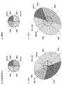
図1(a)は、ターゲット記録層によって反射されたレーザ光(信号光)が、平行光の状態でアナモレンズ等の非点収差素子に入射されたときの信号光と迷光の収束状態を示す図である。なお、“迷光1”は、レーザ光入射面側から見てターゲット記録層よりも一つ奥側にある記録層にて反射されたレーザ光であり、“迷光2”は、ターゲット記録層よりも一つ手前にある記録層にて反射されたレーザ光である。また、同図は、信号光がターゲット記録層にフォーカス合わせされたときの状態を示している。
FIG. 1A is a diagram showing a convergence state of signal light and stray light when laser light (signal light) reflected by a target recording layer is incident on an astigmatism element such as an anamorphic lens in a parallel light state. It is. “Stray light 1” is a laser beam reflected by a recording layer that is one deeper than the target recording layer when viewed from the laser light incident surface side, and “
図示の如く、アナモレンズの作用により、図中の“曲面方向”に信号光が収束することによって面S1に焦線が生じ、さらに、この曲面方向に垂直な図中の“平面方向”に信号光が収束することによって面S2に焦線が生じる。そして、面S1と面S2の間の面S0において、信号光のスポットが最小(最小錯乱円)となる。非点収差法に基づくフォーカス調整では、面S0に光検出器の受光面が置かれる。なお、ここではアナモレンズにおける非点収差作用を簡単に説明するために、便宜上、“曲面方向”と“平面方向”と表現しているが、実際には、互いに異なる位置に焦線を結ぶ作用がアナモレンズによって生じれば良く、図1中の“平面方向”においてアナモレンズが曲率を持っていても良い。なお、アナモレンズに収束状態でレーザ光が入射する場合は、“平面方向”におけるアナモレンズの形状は直線状(曲率半径=∞)となり得る。 As shown in the figure, the signal light converges in the “curved surface direction” in the figure due to the action of the anamorphic lens, thereby generating a focal line on the surface S1, and further, the signal light in the “planar direction” in the figure perpendicular to the curved surface direction. Converges to produce a focal line on the surface S2. And in the surface S0 between the surface S1 and the surface S2, the spot of signal light becomes the minimum (minimum circle of confusion). In focus adjustment based on the astigmatism method, the light receiving surface of the photodetector is placed on the surface S0. Here, in order to simply explain the astigmatism action in the anamorphic lens, it is expressed as “curved surface direction” and “planar direction” for the sake of convenience. It may be generated by an anamorphic lens, and the anamorphic lens may have a curvature in the “plane direction” in FIG. When the laser light is incident on the anamorphic lens in a convergent state, the shape of the anamorphic lens in the “planar direction” can be linear (curvature radius = ∞).
なお、同図(a)に示す如く、迷光1の焦線位置(同図では、非点収差素子による2つの焦線位置の間の範囲を“収束範囲”と示す)は、信号光の焦線位置よりも非点収差素子に接近しており、また、迷光2の焦線位置は、信号光の焦線位置よりも非点収差素子から離れている。
As shown in FIG. 6A, the focal line position of stray light 1 (in the figure, the range between two focal line positions by the astigmatism element is indicated as “convergence range”). It is closer to the astigmatism element than the line position, and the focal line position of the
図1(b)〜(e)は、それぞれ、平行光部分および面S1、S0、S2上における信号光のビーム形状を示す図である。真円で非点収差素子に入射した信号光は、面S1上で楕円となり、面S0上で略真円となった後、面S2上にて再び楕円となる。ここで、面S1上のビーム形状と面S2上のビーム形状は、それぞれの長軸が互いに垂直の関係となっている。 FIGS. 1B to 1E are diagrams showing beam shapes of signal light on the parallel light portion and the surfaces S1, S0, and S2, respectively. The signal light incident on the astigmatism element in a perfect circle becomes an ellipse on the surface S1, becomes a substantially perfect circle on the surface S0, and becomes an ellipse again on the surface S2. Here, the major axis of the beam shape on the surface S1 and the beam shape on the surface S2 are perpendicular to each other.
ここで、同図(a)および(b)のように、平行光部分におけるビームの外周に、反時計方向に8つの位置(位置1〜8:同図では丸囲み数字で表記)を設定すると、位置1〜8を通る光線は、非点収差素子によってそれぞれ収束作用を受ける。なお、位置4と位置8は、曲面方向に平行な直線にて平行光部分のビーム断面を2分割する場合の分割線上に位置しており、位置2と位置6は、平面方向に平行な直線にて平行光部分のビーム断面を2分割する場合の分割線上に位置している。位置1、3、5、7はそれぞれ、位置2、4、6、8によって区分される外周円弧の中間にある。
Here, as shown in FIGS. 9A and 9B, when eight positions (
平行光部分において位置4と位置8を通る光線は、面S1で曲面方向の焦線へと収束された後に面S0へと入射する。このため、これら位置4、8を通る光線は、面S0上において、同図(d)に示す位置4、8を通る。同様に、平行光部分において位置1、3、5、7を通る光線も、面S1にて曲面方向の焦線へと収束された後に面S0へと入射するため、面S0上では、同図(d)に示す位置1、3、5、7を通る。これに対し、平行光部分において位置2、6を通る光線は、面S1で曲面方向の焦線へと収束されずに面S0へと入射する。このため、これら位置2、6を通る光線は、面S0上において、同図(d)に示す位置2、6を通る。
Light rays passing through
図2(b)〜(e)は、それぞれ、平行光部分および面S1、S0、S2上における迷光1のビーム形状と光線通過位置を示す図である。同図(b)に示すように、迷光1の外周にも、上記信号光の場合と同様に8つの位置1〜8を設定すると、これら8つの位置1〜8を通る光線は、曲面方向の焦線および平面方向の焦線の何れかに収束された後に面S0へと入射する。このため、平行光部分において位置1〜8を通る光線は、面S0上において、それぞれ、同図(d)に示す位置1〜8を通る。
FIGS. 2B to 2E are diagrams showing the beam shape and the light beam passage position of the
図3(b)〜(e)は、それぞれ、平行光部分および面S1、S0、S2上における迷光2のビーム形状と光線通過位置を示す図である。同図(b)に示すように、迷光2の外周にも、上記信号光の場合と同様に8つの位置1〜8を設定すると、これら8つの位置1〜8を通る光線は、曲面方向の焦線と平面方向の焦線の何れへも収束されることなく面S0へと入射する。このため、平行光部分において位置1〜8を通る光線は、面S0上において、それぞれ、同図(d)に示す位置1〜8を通る。
FIGS. 3B to 3E are diagrams showing the beam shape and the light beam passage position of the
図4は、以上に説明した平行光部分および面S1、S0、S2上におけるビーム形状と光線の通過位置を、信号光、迷光1および迷光2を対比して示す図である。同図中の(c)の段を対比して分かるとおり、平行光部分において位置1を通過した信号光、迷光1および迷光2の光束は、それぞれ、面S0上において、互いに異なる外周位置を通過する。同様に、平行光部分において位置3,4,5,7,8を通過した信号光、迷光1および迷光2の光束も、面S0において、互いに異なる外周位置を通過する。平行光部分において位置2,6を通過した信号光と迷光2の光束は、面S0において、同じ外周位置を通過する。この場合も、平行光部分において位置2,6を通過した信号光と迷光1の光束は、面S0において、互いに異なる外周位置を通過し、また、平行光部分において位置2、6を通過した迷光1と迷光2の光束は、面S0において、互いに異なる外周位置を通過する。
FIG. 4 is a diagram showing the beam shape and the passage position of the light beam on the parallel light portion and the surfaces S1, S0, and S2 described above in comparison with the signal light, the
次に、以上の現象を考慮して、平行光部分における信号光および迷光1、2の領域分割パターンと、面S0上における信号光および迷光1、2の照射領域との関係について検討する。
Next, considering the above phenomenon, the relationship between the area division pattern of the signal light and
まず、図5(a)に示すように、平行光部分における信号光および迷光1、2を、平面方向と曲面方向に対して45°傾いた2つの直線で分割し、4つの光束領域A〜Dに区分したとする。なお、この分割パターンは、従来の非点収差法に基づく領域分割に対応するものである。
First, as shown in FIG. 5A, the signal light and the
この場合、上述の現象により、光束領域A〜Dの信号光は、面S0上において、同図(b)のように分布する。また、光束領域A〜Dの迷光1および迷光2は、上述の現象により、それぞれ、同図(c)および(d)のように分布する。
In this case, the signal light in the light flux areas A to D is distributed on the surface S0 as shown in FIG. Further, the
ここで、面S0上における信号光と迷光1、2を光束領域毎に取り出すと、各光の分布は、図6(a)ないし(d)のようになる。この場合、各光束領域の信号光には、同じ光束領域の迷光1および迷光2の何れか一方が必ず重なる。このため、各光束領域の信号光を光検出器上のセンサパターンで受光すると、少なくとも、同じ光束領域における迷光1または迷光2が対応するセンサパターンに同時に入射し、これにより検出信号に劣化が生じる。
Here, when the signal light and the
これに対し、図7(a)に示すように、平行光部分における信号光および迷光1、2を、平面方向と曲面方向に平行な2つの直線で分割し、4つの光束領域A〜Dに区分したとする。この場合、上述の現象から、光束領域A〜Dの信号光は、面S0上において、同図(b)のように分布する。また、光束領域A〜Dの迷光1および迷光2は、上述の現象により、それぞれ、同図(c)および(d)のように分布する。
On the other hand, as shown in FIG. 7A, the signal light and the
ここで、面S0上における信号光と迷光1、2を光束領域毎に取り出すと、各光の分布は、図8(a)ないし(d)のようになる。この場合、各光束領域の信号光には、同じ光束領域の迷光1および迷光2の何れも重ならない。このため、各光束領域内の光束(信号光、迷光1、2)を異なる方向に離散させた後に、信号光のみをセンサパターンにて受光するように構成すると、対応するセンサパターンには信号光のみが入射し、迷光の入射を抑止することができる。これにより、迷光による検出信号の劣化を回避することができる。
Here, when the signal light and the
以上のように、信号光および迷光1、2を平面方向と曲面方向に平行な2つの直線で4つの光束領域A〜Dに分割し、これら光束領域A〜Dを通る光を分散させて面S0上において離間させることにより、信号光のみを取り出すことができる。本実施の形態は、この原理を基盤とするものである。
As described above, the signal light and the
図9は、図7(a)に示す4つの光束領域A〜Dを通る光束(信号光、迷光1、2)の進行方向を、それぞれ、異なる方向に、同じ角度だけ変化させたときの、面S0上における信号光と迷光1、2の分布状態を示す図である。ここでは、同図(a)に示すように、光束領域A〜Dを通る光束(信号光、迷光1、2)の進行方向が、それぞれ、方向Da、Db、Dc、Ddに、同じ角度量α(図示せず)だけ変化している。なお、方向Da、Db、Dc、Ddは、平面方向と曲面方向に対して、それぞれ、45°の傾きを持っている。
FIG. 9 shows a case where the traveling directions of the light beams (signal light,
この場合、方向Da、Db、Dc、Ddにおける角度量αを調節することにより、S0平面上において、同図(b)に示すように各光束領域の信号光と迷光1、2を分布させることができる。その結果、図示の如く、信号光のみが存在する信号光領域をS0平面上に設定することができる。この信号光領域に光検出器のセンサパターンを設定することにより、各領域の信号光のみを、対応するセンサパターンにて受光することができる。
In this case, by adjusting the angle amount α in the directions Da, Db, Dc, and Dd, the signal light and the
図10は、センサパターンの配置方法を説明する図である。同図(a)および(b)は、従来の非点収差法に基づく光束の分割方法とセンサパターンを示す図であり、同図(c)および(d)は、上述の原理に基づく光束の分割方法とセンサパターンを示す図である。ここで、トラック方向は、平面方向および曲面方向に対して45°の傾きを持っている。なお、同図(a)および(b)には、説明の便宜上、光束が8つの光束領域a〜hに区分されている。また、トラック溝による回折の像(トラック像)が実線で示され、オフフォーカス時のビーム形状が点線によって示されている。 FIG. 10 is a diagram illustrating a method for arranging sensor patterns. (A) and (b) are diagrams showing a beam splitting method and a sensor pattern based on the conventional astigmatism method, and (c) and (d) in FIG. It is a figure which shows the division | segmentation method and a sensor pattern. Here, the track direction has an inclination of 45 ° with respect to the plane direction and the curved surface direction. In FIGS. 4A and 4B, for convenience of explanation, the light beam is divided into eight light beam regions a to h. Further, an image of diffraction by the track groove (track image) is indicated by a solid line, and a beam shape at the time of off-focus is indicated by a dotted line.
なお、トラック溝による信号光の0次回折像と一次回折像の重なり状態は、波長/(トラックピッチ×対物レンズNA)で求められることが知られており、同図(a)、(b)、(d)のように、4つの光束領域a、d、e、hに一次回折像が収まる条件は、波長/(トラックピッチ×対物レンズNA)>√2となる。 It is known that the overlapping state of the 0th-order diffraction image and the first-order diffraction image of the signal light by the track groove is obtained by wavelength / (track pitch × objective lens NA), and FIGS. , (D), the condition that the first-order diffraction image fits in the four light flux regions a, d, e, and h is wavelength / (track pitch × objective lens NA)> √2.
従来の非点収差法では、光検出器のセンサP1〜P4(4分割センサ)が同図(b)のように設定される。この場合、光束領域a〜hの光強度に基づく検出信号成分をA〜Hで表すと、フォーカスエラー信号FEとプッシュプル信号PPは、
FE=(A+B+E+F)−(C+D+G+H) …(1)
PP=(A+B+G+H)−(C+D+E+F) …(2)
の演算により求まる。
In the conventional astigmatism method, the sensors P1 to P4 (four-divided sensors) of the photodetector are set as shown in FIG. In this case, when the detection signal components based on the light intensity of the light flux areas a to h are represented by A to H, the focus error signal FE and the push-pull signal PP are
FE = (A + B + E + F) − (C + D + G + H) (1)
PP = (A + B + G + H)-(C + D + E + F) (2)
It is obtained by the operation of
これに対し、上記図9(b)の分布状態では、上述の如く、信号光領域内に、図10(c)の状態で信号光が分布している。この場合、同図(a)に示す光束領域a〜hを通る信号光は、同図(d)のようになる。すなわち、同図(a)の光束領域a〜hを通る信号光は、光検出器のセンサパターンが置かれる面S0上では、同図(d)に示す光束領域a〜hへと導かれる。 On the other hand, in the distribution state of FIG. 9B, the signal light is distributed in the state of FIG. 10C in the signal light region as described above. In this case, the signal light passing through the light beam areas a to h shown in FIG. That is, the signal light passing through the light flux areas a to h in FIG. 5A is guided to the light flux areas a to h shown in FIG. 4D on the surface S0 on which the sensor pattern of the photodetector is placed.
したがって、同図(d)に示す光束領域a〜hの位置に、同図(d)に重ねて示す如くセンサP11〜P18を設定すれば、同図(b)の場合と同様の演算処理によって、フォーカスエラー信号とプッシュプル信号を生成することができる。すなわち、この場合も、光束領域a〜hの光束を受光するセンサパターンからの検出信号をA〜Hで表すと、同図(b)の場合と同様、フォーカスエラー信号FEとプッシュプル信号PPは、上記式(1)、(2)の演算により取得することができる。 Therefore, if the sensors P11 to P18 are set at the positions of the light beam areas a to h shown in FIG. 4D so as to overlap with each other in the same figure (d), the same calculation process as in FIG. A focus error signal and a push-pull signal can be generated. That is, also in this case, when the detection signals from the sensor patterns that receive the light beams in the light beam regions a to h are represented by A to H, the focus error signal FE and the push-pull signal PP are expressed as in the case of FIG. , And can be obtained by the calculations of the above formulas (1) and (2).
以上のように、本原理によれば、平行光部分における信号光および迷光1、2を、図1の平面方向と曲面方向に平行な2つの直線で4つの光束領域A〜Dに分割し、これら光束領域A〜Dを通る光を分散させ、さらに、分散させた後の各光束領域A〜Dにおける信号光を、2分割された受光部(2分割センサ)によって個別に受光することにより、従来の非点収差法に基づく場合と同様の演算処理にて、フォーカスエラー信号とプッシュプル信号(トラッキングエラー信号)を生成することができる。
As described above, according to the present principle, the signal light and the
ところで、実際の光学系では、図10(d)に示す8個のセンサから出力される検出信号は、各センサに対応するI/Vアンプに通された後、後段の回路に出力される。かかるI/Vアンプは、センサから出力される検出信号(電流信号)を電圧信号に変換し、さらに、この電圧信号を増幅させて後段の回路に出力する。 By the way, in an actual optical system, detection signals output from the eight sensors shown in FIG. 10D are output to a subsequent circuit after being passed through an I / V amplifier corresponding to each sensor. Such an I / V amplifier converts a detection signal (current signal) output from the sensor into a voltage signal, amplifies the voltage signal, and outputs the amplified voltage signal to a subsequent circuit.
このとき、各センサに対応するI/Vアンプにおいて、固有のノイズが発生するため、I/Vアンプから出力される電圧信号は、このノイズによって劣化することとなる。このようなアンプノイズは、後段回路での信号生成に用いられるI/Vアンプの数に応じて増加する。例えば、図10(d)に示す8個のセンサが用いられる場合、従来の4分割センサ(4個のセンサ)に比べ、信号光の光量の総和により生成される再生RF信号に重畳されるアンプノイズに影響するI/Vアンプの数は2倍となる。このとき、S/N(信号雑音比)は3dB劣化することとなる。 At this time, inherent noise is generated in the I / V amplifier corresponding to each sensor, so that the voltage signal output from the I / V amplifier is degraded by this noise. Such amplifier noise increases in accordance with the number of I / V amplifiers used for signal generation in the subsequent circuit. For example, when eight sensors shown in FIG. 10 (d) are used, an amplifier that is superimposed on a reproduction RF signal generated by the total amount of signal light compared to a conventional four-divided sensor (four sensors). The number of I / V amplifiers affecting noise is doubled. At this time, the S / N (signal to noise ratio) deteriorates by 3 dB.
かかる再生RF信号の劣化は、再生RF信号の生成に用いるI/Vアンプの個数を削減することにより抑制される。再生RF信号の劣化を抑制するための構成は、以下の実施例にて明らかにする。 Such deterioration of the reproduction RF signal is suppressed by reducing the number of I / V amplifiers used to generate the reproduction RF signal. The configuration for suppressing the deterioration of the reproduction RF signal will be clarified in the following examples.
<実施例>
以下、上記原理に基づく実施例について説明する。
<Example>
Hereinafter, embodiments based on the above principle will be described.
図11に、本実施例に係る光ピックアップ装置の光学系を示す。なお、同図には、便宜上、関連する回路構成が併せて図示されている。また、同図中のディスクには、複数の記録層が積層して配置されている。 FIG. 11 shows an optical system of the optical pickup device according to the present embodiment. In the drawing, related circuit configurations are also shown for convenience. In addition, a plurality of recording layers are stacked on the disk in FIG.
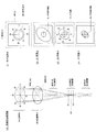
図中、再生回路203、サーボ回路204およびコントローラ205は、光ピックアップ装置を搭載する光ディスク装置側に配される。I/Vアンプ部201は、光ピックアップ装置側に配されても良く、あるいは、光ディスク装置側に配されても良い。また、信号演算回路202の全部または一部が光ピックアップ装置側に配されても良く、あるいは、光ディスク装置側に配されても良い。光検出器113が、IC(Integrated Circuit)部を備えるPDICによって構成される場合、I/Vアンプ部201は、光検出器113のIC部に含まれる。この場合、信号演算回路202の一部が光検出器113のIC部に含まれても良い。
In the figure, a reproducing
図示の如く、光ピックアップ装置の光学系は、半導体レーザ101と、偏光ビームスプリッタ102と、コリメートレンズ103と、レンズアクチュエータ104と、立ち上げミラー105と、1/4波長板106と、アパーチャ107と、対物レンズ108と、ホルダ109と、対物レンズアクチュエータ110と、検出レンズ111と、角度調整素子112と、光検出器113を備えている。
As shown in the figure, the optical system of the optical pickup device includes a
半導体レーザ101は、所定波長のレーザ光を出射する。半導体レーザ101から出射されるレーザ光の広がり角は、水平広がり角と垂直広がり角が異なっている。
The
偏光ビームスプリッタ102は、半導体レーザ101から入射されるレーザ光(S偏光)を略全反射するとともに、コリメートレンズ103側から入射されるレーザ光(P偏光)を略全透過する。コリメートレンズ103は、偏光ビームスプリッタ102側から入射されるレーザ光を平行光に変換する。
The
レンズアクチュエータ104は、サーボ回路203から入力されるサーボ信号に応じてコリメートレンズ103を光軸方向に変位させる。これにより、レーザ光に生じる収差が補正される。立ち上げミラー105は、コリメートレンズ103側から入射されたレーザ光を対物レンズ108に向かう方向に反射する。
The
1/4波長板106は、ディスクへと向かうレーザ光を円偏光に変換するとともに、ディスクからの反射光をディスクへ向かう際の偏光方向に直交する直線偏光に変換する。これにより、ディスクによって反射されたレーザ光は、偏光ビームスプリッタ102を透過する。
The quarter-
アパーチャ107は、対物レンズ108に対するレーザ光の有効径が適正となるように、レーザ光のビーム形状を円形形状に調整する。対物レンズ108は、レーザ光をディスク内のターゲット記録層に適正に収束できるよう設計されている。ホルダ109は、1/4波長板106と対物レンズ108を一体的に保持する。対物レンズアクチュエータ110は、従来周知の電磁駆動回路によって構成され、当該回路のうち、フォーカスコイル等のコイル部がホルダ109に装着されている。
The
検出レンズ111は、ディスクからの反射光に非点収差を導入する。すなわち、検出レンズ111は、図1の非点収差素子に相当する。検出レンズ111は、平面方向と曲面方向が、ディスクからのトラック像に対してそれぞれ45°の傾きとなるよう配置される。
The
角度調整素子112は、レーザ光の入射面にホログラムパターンが形成されている。これにより、検出レンズ111側から入射されたレーザ光の進行方向が変化させられる。なお、角度調整素子112については、追って図12を参照して説明する。
The
光検出器113は、受光面上に複数のセンサを有する。光検出器113は、これらセンサが図1の面S0の位置に位置づけられるように配置される。なお、光検出器113のセンサパターンについては、追って図14を参照して説明する。
The
I/Vアンプ部201は、10個のI/Vアンプ(図示せず)を有する。これらI/Vアンプは、光検出器113の受光面上のセンサから出力される検出信号を電圧信号に変換し、さらに、この電圧信号を増幅させて、信号演算回路202に出力する。
The I /
信号演算回路202は、I/Vアンプ部201から入力された電圧信号に基づく演算処理により、再生RF信号、フォーカスエラー信号、プッシュプル信号(トラッキングエラー信号)および位置ずれ信号(角度調整素子112と光検出器113の位置ずれを示す信号)を生成する。生成された再生RF信号は再生回路203とサーボ回路204に送られ、フォーカスエラー信号およびプッシュプル信号(トラッキングエラー信号)はサーボ回路204に送られ、位置ずれ信号はコントローラ205に送られる。なお、信号演算回路202で行われるこれらの信号の生成については、追って図14を参照して説明する。
The
再生回路203は、信号演算回路202から入力された再生RF信号を復調して再生データを生成する。サーボ回路204は、信号演算回路202から入力されたフォーカスエラー信号とプッシュプル信号(トラッキングエラー信号)から、フォーカスサーボ信号とトラッキングサーボ信号を生成し、これらを対物レンズアクチュエータ110に出力する。また、サーボ回路204は、信号演算回路202から入力された再生RF信号の品質が最良になるよう、レンズアクチュータ104にサーボ信号を出力する。コントローラ205は、内蔵メモリに格納されたプログラムに従って各部を制御する。
The
図12(a)は、角度調整素子112をディスクからの反射光の進行方向に見たときの平面図である。
FIG. 12A is a plan view when the
角度調整素子112は、正方形形状の透明板にて形成され、光入射面にブレーズ型によるホログラムパターンが形成されている。光入射面は、図示の如く、4つのホログラム領域112a〜112dに区分されている。これらホログラム領域112a〜112dに、それぞれ、図9(a)の光束領域A〜Dを通過したレーザ光(信号光、迷光1、2)が入射するよう、角度調整素子112が検出レンズ111の後段に配置される。
The
ホログラム領域112a〜112dは、入射されたレーザ光(信号光、迷光1、2)を、それぞれ、1次回折作用により方向Va1〜Vd1に回折させ、2次回折作用により方向Va2〜Vd2に回折させる。方向Va1〜Vd1は、図9(a)の方向Da〜Ddに一致しており、方向Va2〜Vd2もまた、図9(a)の方向Da〜Ddに一致している。また、各領域における1次回折角は互いに同じであり、各領域における2次回折角も互いに同じとなっている。2次回折角は1次回折角よりも大きい。これにより、ホログラム領域112a〜112dの1次回折作用によって、検出レンズ111から入射されたレーザ光(信号光、迷光1、2)は、光検出器113の受光面上で、図9(b)のように分布する。また、ホログラム領域112a〜112dの2次回折作用により、検出レンズ111から入射されたレーザ光(信号光、迷光1、2)は、光検出器113の受光面上で、図9(b)よりも広がって分布する。
The
図12(b)は、角度調整素子112の回折作用による信号光の分布を示す図である。なお、図中、破線で囲まれた扇型部分は、1次回折作用による迷光1、2を示している。
FIG. 12B is a diagram showing the distribution of signal light due to the diffraction effect of the
図示の如く、1次回折作用による信号光(以下、「1次信号光」という)の信号光領域は、図9(b)と同様である。これに対し、2次回折作用による信号光(以下、「2次信号光」という)の信号光領域は、1次信号光の信号光領域の外側に位置している。また、2次回折作用による迷光1、2(図示せず)は、2次信号光の信号光領域の外側に広がっている。
As shown in the drawing, the signal light region of signal light (hereinafter referred to as “first-order signal light”) by the first-order diffraction action is the same as that in FIG. On the other hand, the signal light region of signal light (hereinafter referred to as “second-order signal light”) by the second-order diffraction action is located outside the signal light region of the primary signal light. Further,
図13(a)は、ブレーズ型のホログラムパターンの模式図である。ブレーズ型のホログラムパターンでは、回折効率は、ホログラムパターンのブレーズ高さHにより調整され、回折角度は、ホログラムパターンのピッチWにより調整される。 FIG. 13A is a schematic diagram of a blazed hologram pattern. In a blazed hologram pattern, the diffraction efficiency is adjusted by the blaze height H of the hologram pattern, and the diffraction angle is adjusted by the pitch W of the hologram pattern.
図13(b)は、ブレーズ型のホログラムパターンにおいて、ブレーズ高さと回折効率の関係を示す図である。角度調整素子112に形成されたホログラムパターンのブレーズ高さHは、図中の“設定値”に設定されている。このとき、角度調整素子112の1次の回折効率は9%であり、2次の回折効率は83%となっている。
FIG. 13B is a diagram showing the relationship between blaze height and diffraction efficiency in a blazed hologram pattern. The blaze height H of the hologram pattern formed on the
図14は、光検出器113の受光面上に配されるセンサパターンを示す図である。なお、同図には、I/Vアンプ部201内のI/Vアンプ21〜26、31〜34が、併せて示されている。
FIG. 14 is a diagram showing a sensor pattern arranged on the light receiving surface of the
図示の如く、光検出器113の受光面上には、図12(b)に示した1次信号光を受光するためのセンサP21〜P26と、図12(b)に示した2次信号光を受光するためのセンサP31〜P38が配されている。なお、1次信号光と2次信号光が、それぞれセンサP21〜26とセンサP31〜P38に位置づけられるよう、ホログラムパターンのピッチWが設定されている。
As shown in the drawing, on the light receiving surface of the
センサP21は、図10(d)に示したセンサパターンのうち、センサP11とP12に入射するレーザ光を合わせて受光する大きさとなっている。同様に、センサP26は、図10(d)に示したセンサパターンのうち、センサP17とP18に入射するレーザ光を合わせて受光する大きさとなっている。センサP32とP35、センサP33とP38、センサP34とP37、センサP31とP36は、それぞれ、検出信号が加算されるよう短絡されている。 The sensor P21 is sized to receive the laser beams incident on the sensors P11 and P12 in the sensor pattern shown in FIG. Similarly, the sensor P26 is sized to receive the laser beams incident on the sensors P17 and P18 in the sensor pattern shown in FIG. Sensors P32 and P35, sensors P33 and P38, sensors P34 and P37, and sensors P31 and P36 are short-circuited so that detection signals are added.
センサP21〜P26から出力される6つの検出信号B0、C2、A1、C1、A2、D0は、それぞれ、I/Vアンプ部201内のI/Vアンプ21〜26に入力される。センサP32とP35、センサP33とP38、センサP34とP37、センサP31とP36から出力される4つの検出信号MA、MB、MC、MDは、それぞれ、I/Vアンプ部201内のI/Vアンプ31〜34に入力される。各I/Vアンプから出力される電圧信号は、後述する信号演算回路202で行われる演算に用いられる。
The six detection signals B0, C2, A1, C1, A2, and D0 output from the sensors P21 to P26 are input to the I /
次に、信号演算回路202で行われる演算について説明する。なお、以下の式において、演算に用いられる電圧信号は、便宜上、I/Vアンプを通される前の電流信号を表す記号と同じ記号で表わされている。
Next, the calculation performed by the
再生RF信号と、溝外乱対応のフォーカスエラー信号FEと、DPP(Differential Push-Pull)法によるトラッキングエラー信号DPPと、光検出器113のZ軸正方向の位置ずれ信号PD1とY軸負方向の位置ずれ信号PD2と、角度調整素子112のY軸負方向の位置ずれ信号HOE1とZ軸正方向の位置ずれ信号HOE2は、以下の式により算出される。
The reproduction RF signal, the focus error signal FE corresponding to the groove disturbance, the tracking error signal DPP by the DPP (Differential Push-Pull) method, the Z-axis positive position shift signal PD1 of the
RF=MA+MB+MC+MD
FE={(MA+MC)−(MB+MD)}
+k1{(A1+C1)−(A2+C2)}
DPP={(MA+MD)−(MB+MC)}
+k2{(A1+C2)−(A2+C1)}
PD1={(MA+MD)−(MB+MC)}
/{(MA+MD)+(MB+MC)}
PD2={(MA+MB)−(MC+MD)}
/{(MA+MB)+(MC+MD)}
HOE1=(B0−D0)/(B0+D0)
HOE2={(C1+C2)−(A1+A2)}
/{(C1+C2)+(A1+A2)}
RF = MA + MB + MC + MD
FE = {(MA + MC)-(MB + MD)}
+ K1 {(A1 + C1)-(A2 + C2)}
DPP = {(MA + MD)-(MB + MC)}
+ K2 {(A1 + C2)-(A2 + C1)}
PD1 = {(MA + MD)-(MB + MC)}
/ {(MA + MD) + (MB + MC)}
PD2 = {(MA + MB)-(MC + MD)}
/ {(MA + MB) + (MC + MD)}
HOE1 = (B0−D0) / (B0 + D0)
HOE2 = {(C1 + C2)-(A1 + A2)}
/ {(C1 + C2) + (A1 + A2)}
なお、上記式におけるk1、k2が調整されることにより、上記フォーカスエラー信号における溝外乱が抑制され、上記トラッキングエラー信号DPPのDC成分が抑制される。なお、k1の調整方法および上記FEの演算により溝外乱の抑制が可能となることは、出願人が先に出願した特願2009−013592号に記載されている。また、k2の調整方法および上記DPPの演算によりDC成分の抑制が可能となることは、出願人が先に出願した特願2009−129668号に記載されている。 By adjusting k1 and k2 in the above equation, groove disturbance in the focus error signal is suppressed, and the DC component of the tracking error signal DPP is suppressed. Incidentally, it is described in Japanese Patent Application No. 2009-013592 filed earlier by the applicant that the groove disturbance can be suppressed by the k1 adjustment method and the FE calculation. Further, it is described in Japanese Patent Application No. 2009-129668 filed earlier by the applicant that the DC component can be suppressed by the k2 adjustment method and the DPP calculation.
また、位置ずれ信号PD1、PD2の値が0になるよう光検出器113が位置調整され、位置ずれ信号HOE1、HOE2の値が0になるよう角度調整素子112が位置調整される。すなわち、光ピックアップ装置の製造時に、これらの信号が評価装置に送られる。そして、製造者によりこれらの信号がモニタされ、これらの信号の値が0になるように、光検出器113と角度調整素子112が位置調整される。なお、これらの信号を用いた光検出器113と角度調整素子112の位置調整方法は、出願人が先に出願した特願2009−177046号に記載されている。
Further, the position of the
また、上記式の他、DPD(Differential Phase Detection)法によるトラッキングエラー信号DPDも、MA〜MDを用いて、従来周知の演算により算出される。 In addition to the above formula, a tracking error signal DPD by a DPD (Differential Phase Detection) method is also calculated by a conventionally known calculation using MA to MD.
以上、本実施例によれば、ディスク内に配された記録層のうちターゲット記録層から反射された信号光と、当該ターゲット記録層の上および下の記録層から反射された迷光1、2とが、光検出器113の受光面(オンフォーカス時に信号光スポットが最小錯乱円になる面S0)上において、互いに重なり合うのを抑制することができる。具体的には、受光面(面S0)上における信号光と迷光1、2の分布を、図12(b)の状態にすることができる。したがって、図12(b)の1次信号光の信号光領域と2次信号光の信号光領域に、図14に示すセンサパターンを配置することにより、センサP21〜P26、P31〜P38によって、対応する信号光を適正に受光することができる。このため、迷光による検出信号の劣化を抑制することができる。
As described above, according to the present embodiment, the signal light reflected from the target recording layer among the recording layers arranged in the disk, and the
なお、図12(b)を参照して分かるとおり、1次信号光の信号光領域には、迷光が重ならない。よって、図14のセンサP21〜P26に迷光が掛かるのを回避することができる。これに対し、図12(b)に示す1次回折作用による迷光の領域は、実際には、同図に破線で示す領域よりも広がっているため、2次信号光の照射領域に1次回折作用による迷光が掛かることになる。しかし、この場合も、1次回折光の回折効率は9%程度に抑えられているため、2次信号光の強度に比べ、1次回折作用による迷光の強度は顕著に小さくなる。したがって、図14のセンサP31〜P38からは、1次回折作用による迷光の影響を殆ど受けない信号が出力される。 As can be seen with reference to FIG. 12B, stray light does not overlap the signal light region of the primary signal light. Therefore, it is possible to avoid stray light from being applied to the sensors P21 to P26 in FIG. On the other hand, the stray light region due to the first-order diffraction action shown in FIG. 12B is actually wider than the region indicated by the broken line in FIG. The stray light by the action is applied. However, also in this case, since the diffraction efficiency of the first-order diffracted light is suppressed to about 9%, the intensity of stray light due to the first-order diffractive action is significantly smaller than the intensity of the second-order signal light. Accordingly, signals that are hardly affected by stray light due to the first-order diffraction action are output from the sensors P31 to P38 in FIG.
加えて、本実施例によれば、図14に示すように、1次信号光を受光するためのセンサP21〜P26から出力された検出信号が、6個のI/Vアンプ21〜26に入力され、2次信号光を受光するためのセンサP31〜P38から出力された検出信号が、4個のI/Vアンプ31〜34に入力される。こうして、各I/Vアンプから出力された電圧信号に基づいて、上記式の演算が行われる。こうすると、再生RF信号に用いられる検出信号MA〜MDのI/V変換後の電圧信号には、4個のI/Vアンプによるアンプノイズしか重畳されない。よって、図10(d)に示す8個のセンサP11〜P18からの出力信号を8個のI/VアンプでI/V変換した電圧信号から再生RF信号を生成する場合に比べて、再生RF信号に重畳するアンプノイズが低減されるため、より精度の高い再生RF信号を得ることができる。
In addition, according to the present embodiment, as shown in FIG. 14, the detection signals output from the sensors P21 to P26 for receiving the primary signal light are input to the six I /
なお、本実施例では、図14に示すように、図8(d)のセンサP11、P12と、センサP17、P18がそれぞれ一体化されてセンサP21とP26とされているため、位置ずれ信号HOE1に重畳するアンプノイズも低減される。 In the present embodiment, as shown in FIG. 14, the sensors P11 and P12 and the sensors P17 and P18 in FIG. 8D are integrated to form the sensors P21 and P26. Amplifier noise superimposed on the signal is also reduced.
また、以上の効果を、ディスクによって反射されたレーザ光の光路中、すなわち、図11の構成では検出レンズ111と光検出器113の間に、角度調整素子112を配置するのみで達成することができる。したがって、本実施例によれば、簡素な構成にて効果的に迷光による影響を除去することができ、かつ、信号演算に用いられる電圧信号に重畳するアンプノイズを抑制することができる。
Further, the above effect can be achieved only by arranging the
なお、上記原理による迷光除去効果は、図15に示すように、迷光1の平面方向の焦線位置が面S0(信号光のスポットが最小錯乱円となる面)よりも非点収差素子に接近した位置にあり、且つ、迷光2の曲面方向の焦線位置が面S0よりも非点収差素子から離れた位置にあるときに奏され得るものである。すなわち、この関係が満たされていれば、信号光と迷光1、2の分布は上記図8に示す状態となり、面S0において、信号光と迷光1、2が重なり合わないようすることができる。換言すれば、この関係が満たされる限り、たとえ、信号光の曲面方向の焦線位置よりも迷光1の平面方向の焦線位置が面S0に接近し、あるいは、信号光の平面方向の焦線位置よりも迷光2の曲面方向の焦線位置が面S0に接近したとしても、上記原理に基づく本発明ないし実施例の効果は奏され得る。
As shown in FIG. 15, the stray light removal effect based on the above principle is such that the focal line position in the plane direction of the
<変更例>
上記実施例では、ブレーズ型のホログラムパターンを有する角度調整素子112が用いられたが、ステップ型のホログラムパターンを有する角度調整素子112が用いられても良い。また、上記実施例では、光検出器113により1次信号光と2次信号光を受光するようにしたが、他の2つの回折次数の信号光を受光するようにしても良い。
<Example of change>
In the above embodiment, the
以下に、ステップ型のホログラムパターンを有する角度調整素子112を用いて、0次回折作用による信号光と1次回折作用による信号光を光検出器113で受光する場合の構成例を示す。
Hereinafter, a configuration example in the case where the
図13(c)は、ステップ型のホログラムパターンの模式図である。ステップ型のホログラムパターンでは、回折効率は、ホログラムパターンのステップ数と1ステップあたりの高さHにより調整され、回折角度は、ホログラムパターンのピッチWにより調整される。本変更例では、4ステップ型のホログラムが用いられる。 FIG. 13C is a schematic diagram of a step-type hologram pattern. In the step type hologram pattern, the diffraction efficiency is adjusted by the number of steps of the hologram pattern and the height H per step, and the diffraction angle is adjusted by the pitch W of the hologram pattern. In this modified example, a four-step hologram is used.
図13(d)は、4ステップ型のホログラムにおいて、1ステップあたりの高さと回折効率の関係を示す図である。本変更例では、角度調整素子112の0次の回折効率が70%であり、1次の回折効率が15%となるよう、1ステップあたりの高さHが“設定値1”に設定されている。また、ホログラムに入射するレーザ光に対する回折光の利用効率が低下するものの、0次の回折効率が10%であり、1次の回折効率が70%となるよう、1ステップあたりの高さが“設定値2”に設定されても良い。
FIG. 13D is a diagram showing the relationship between the height per step and the diffraction efficiency in a four-step hologram. In this modification, the height H per step is set to “set
図16は、本変更例における光検出器113の受光面上に配されたセンサパターンを示す図である。同図(a)、(b)は、それぞれ、図14(d)において、1ステップあたりの高さHが、“設定値1”、“設定値2”とされた場合を示す図である。なお、図16(a)、(b)のセンサパターンは同じであるため、以下、センサパターンについては、同図(a)についてのみ説明する。
FIG. 16 is a diagram showing a sensor pattern arranged on the light receiving surface of the
同図(a)を参照して、光検出器113の受光面上には、上記実施例で示した1次信号光を受光するためのセンサP21〜P26に加えて、センサP21〜P26の内側の中央領域に、図10(b)に示した従来周知の4分割センサP1〜P4が配されている。センサP1〜P4は、0次回折作用による信号光(以下、「0次信号光」という)を受光する。なお、1次信号光の分布が、センサP21〜P26に位置づけられるよう、ホログラムパターンのピッチWが設定されている。
Referring to FIG. 5A, on the light receiving surface of the
センサP1〜P4から出力される検出信号I1〜I4は、それぞれ、I/Vアンプ部201内のI/Vアンプ(図示せず)に入力される。各I/Vアンプから出力される電圧信号は、信号演算回路202で行われる演算に用いられる。
Detection signals I1 to I4 output from the sensors P1 to P4 are input to an I / V amplifier (not shown) in the I /
次に、信号演算回路202で行われる演算について説明する。なお、以下の式において、演算に用いられる電圧信号は、便宜上、I/Vアンプを通される前の電流信号を表す記号と同じ記号で表わされている。
Next, the calculation performed by the
同図(a)のセンサパターンの再生RF信号は、以下の式により算出される。 The reproduction RF signal of the sensor pattern in FIG.
RF=I1+I2+I3+I4 RF = I1 + I2 + I3 + I4
同図(b)のセンサパターンの再生RF信号は、以下の式により算出される。 The reproduction RF signal of the sensor pattern in FIG. 5B is calculated by the following equation.
RF=A1+A2+B0+C1+C2+D0 RF = A1 + A2 + B0 + C1 + C2 + D0
その他、同図(a)、(b)のセンサパターンの場合に共通して、溝外乱対応のフォーカスエラー信号FEと、DPP(Differential Push-Pull)法によるトラッキングエラー信号DPPと、光検出器113のZ軸正方向の位置ずれ信号PD1とY軸負方向の位置ずれ信号PD2と、角度調整素子112のY軸負方向の位置ずれ信号HOE1とZ軸正方向の位置ずれ信号HOE2は、以下の式により算出される。
In addition, the focus error signal FE corresponding to the groove disturbance, the tracking error signal DPP by the DPP (Differential Push-Pull) method, and the
FE={(I1+I3)−(I2+I4)}
+k1{(A1+C1)−(A2+C2)}
DPP={(I1+I4)−(I2+I3)}
+k2{(A1+C2)−(A2+C1)}
PD1={(I1+I4)−(I2+I3)}
/{(I1+I4)+(I2+I3)}
PD2={(I1+I2)−(I3+I4)}
/{(I1+I2)+(I3+I4)}
HOE1=(B0−D0)/(B0+D0)
HOE2={(C1+C2)−(A1+A2)}
/{(C1+C2)+(A1+A2)}
FE = {(I1 + I3)-(I2 + I4)}
+ K1 {(A1 + C1)-(A2 + C2)}
DPP = {(I1 + I4)-(I2 + I3)}
+ K2 {(A1 + C2)-(A2 + C1)}
PD1 = {(I1 + I4)-(I2 + I3)}
/ {(I1 + I4) + (I2 + I3)}
PD2 = {(I1 + I2)-(I3 + I4)}
/ {(I1 + I2) + (I3 + I4)}
HOE1 = (B0−D0) / (B0 + D0)
HOE2 = {(C1 + C2)-(A1 + A2)}
/ {(C1 + C2) + (A1 + A2)}
なお、上記式におけるk1、k2が調整されることにより、上記フォーカスエラー信号における溝外乱が抑制され、上記トラッキングエラー信号DPPのDC成分が抑制される。 By adjusting k1 and k2 in the above equation, groove disturbance in the focus error signal is suppressed, and the DC component of the tracking error signal DPP is suppressed.
なお、k1の調整方法および上記FEの演算により溝外乱の抑制が可能となることは、出願人が先に出願した特願2009−013592号に記載されている。また、k2の調整方法および上記DPPの演算によりDC成分の抑制が可能となることは、出願人が先に出願した特願2009−129668号に記載されている。位置ずれ信号PD1、PD2、HOE1、HOE2を用いて光検出器113と角度調整素子112の位置調整が行われる(特願2009−177046参照)。
Incidentally, it is described in Japanese Patent Application No. 2009-013592 filed earlier by the applicant that the groove disturbance can be suppressed by the k1 adjustment method and the FE calculation. Further, it is described in Japanese Patent Application No. 2009-129668 filed earlier by the applicant that the DC component can be suppressed by the k2 adjustment method and the DPP calculation. Position adjustment of the
上記式の他、DPD(Differential Phase Detection)法によるトラッキングエラー信号DPDも、MA〜MDを用いて、従来周知の演算により算出される。 In addition to the above formula, a tracking error signal DPD by a DPD (Differential Phase Detection) method is also calculated by a conventionally known calculation using MA to MD.
以上、本変更例においても、迷光による検出信号の劣化が抑制され得る。ただし、図16(a)、(b)に示す2つの変更例では、何れも、0次回折作用による迷光が全てのセンサに掛かることになる。図16(a)の変更例では、0次光の回折効率が高く設定されているため、迷光による影響が大きくなる。これに対し、図16(b)の変更例では、0次光の回折効率が低く設定されているため、迷光による影響は小さい。よって、これら2つの変更例では、図16(b)の変更例の方が、より精度の高い信号を得ることができる。 As described above, also in this modified example, deterioration of the detection signal due to stray light can be suppressed. However, in the two modified examples shown in FIGS. 16A and 16B, stray light due to the 0th-order diffraction action is applied to all sensors. In the modified example of FIG. 16A, since the diffraction efficiency of the 0th-order light is set high, the influence of stray light becomes large. On the other hand, in the modified example of FIG. 16B, the diffraction efficiency of 0th-order light is set low, so that the influence of stray light is small. Therefore, in these two modified examples, the modified example in FIG. 16B can obtain a signal with higher accuracy.
加えて、本変更例によれば、図16(a)、(b)に示すように、0次信号光を受光するためのセンサP1〜P4から出力された検出信号が、4個のI/Vアンプ入力され、1次信号光を受光するためのセンサP21〜P26から出力された検出信号が、6個のI/Vアンプに入力される。こうして、各I/Vアンプから出力された電圧信号に基づいて、上記式の演算が行われる。こうすると、例えば、同図(a)の場合の再生RF信号に用いられる検出信号I1〜I4には、4個のI/Vアンプによるアンプノイズしか重畳されない。また、同図(b)の場合の再生RF信号に用いられる検出信号A1、A2、B0、C1、C2、D0には、6個のI/Vアンプによるアンプノイズしか重畳されない。よって、図10(d)の場合に比べて、再生RF信号に重畳するアンプノイズが低減されるため、より精度の高い再生RF信号を得ることができる。 In addition, according to this modified example, as shown in FIGS. 16A and 16B, the detection signals output from the sensors P1 to P4 for receiving the zero-order signal light are four I / Os. The detection signals output from the sensors P21 to P26 that are input to the V amplifier and receive the primary signal light are input to the six I / V amplifiers. Thus, the calculation of the above equation is performed based on the voltage signal output from each I / V amplifier. In this way, for example, only the amplifier noise due to the four I / V amplifiers is superimposed on the detection signals I1 to I4 used for the reproduction RF signal in the case of FIG. In addition, only the amplifier noise due to the six I / V amplifiers is superimposed on the detection signals A1, A2, B0, C1, C2, and D0 used for the reproduction RF signal in the case of FIG. Therefore, compared with the case of FIG. 10D, the amplifier noise superimposed on the reproduction RF signal is reduced, so that a reproduction RF signal with higher accuracy can be obtained.
また、本変更例によれば、角度調整素子112のレーザ光の利用効率は、図16(a)の場合85%、図16(b)の場合80%となり、上記実施例の利用効率90%に比べてやや低くなる。しかしながら、角度調整素子112がステップ型のホログラムパターンにより形成されているため、上記実施例のブレーズ型のホログラムパターンが用いられる場合に比べ、より安価に角度調整素子112を作成することができる。
Further, according to this modification, the utilization efficiency of the laser beam of the
以上、本発明の実施例および変更例について説明したが、本発明は、上記実施例および変更例に制限されるものではなく、また、本発明の実施形態も上記以外に種々の変更が可能である。 As mentioned above, although the Example and modified example of this invention were demonstrated, this invention is not restrict | limited to the said Example and modified example, Moreover, various changes are possible for embodiment of this invention besides the above. is there.
たとえば、上記実施例および変更例では、ホログラム領域112a〜112dに、レーザ光の進行方向を一定角度だけ変化させる角度付与の回折作用のみを持たせるようにしたが、角度付与の他、検出レンズ111による非点収差作用をも同時に発揮するホログラムパターンを、ホログラム領域112a〜112dに設定しても良い。また、角度調整素子112の光入射面に上記角度付与のためのホログラムパターンを形成し、非点収差作用を持たせるためのホログラムパターンを角度調整素子112の光出射面に持たせるようにしても良い。こうすると、検出レンズ111を省略することができ、部品点数とコストの削減を図ることができる。
For example, in the above-described embodiments and modifications, the
また、上記実施例では、センサP21、P26から出力される検出信号B0、D0は、角度調整素子112の位置ずれ信号HOE1、HOE2を算出するための演算式でのみ用いられる。このため、角度調整素子112の位置ずれ信号が生成される必要がなければ、センサP21、P26を省略し、センサパターンを簡素にすることができる。
In the above embodiment, the detection signals B0 and D0 output from the sensors P21 and P26 are used only in arithmetic expressions for calculating the positional deviation signals HOE1 and HOE2 of the
また、上記変更例では、上述のとおり、0次回折作用による迷光が、センサP1〜P4の他、センサP21〜P26にも入射する。このように、0次回折作用による迷光が入射することにより、センサP21〜P26からの検出信号の劣化が問題となる場合には、角度調整素子112の回折角度を大きくして、センサP21〜P26の位置をセンサP1〜P4の位置からさらに外側に離しても良い。こうすると、センサP21〜P26にて1次信号光を受光しながら、センサP21〜P26に入射する0次回折作用による迷光1、2の光量を低減させることができる。また、この場合、角度調整素子112の回折効率が調整されても良い。例えば、0次の回折効率が小さく設定されれば、センサP21〜P26に入射する0次回折作用による迷光1、2の光量を低減させることができる。
Moreover, in the said modification, as above-mentioned, the stray light by a 0th-order diffraction action injects into sensors P21-P26 besides sensors P1-P4. As described above, when the stray light due to the 0th-order diffraction action is incident and deterioration of the detection signal from the sensors P21 to P26 becomes a problem, the diffraction angle of the
また、上記変更例では、上記の如く、DPP法によるトラッキングエラー信号DPPが設定されたが、センサP1〜P4に入射する0次回折作用の迷光1、2によって、検出信号I1〜I4の劣化が問題となる場合、信号DPPは、以下の式により算出されても良い。
In the above modification, the tracking error signal DPP by the DPP method is set as described above. However, the detection signals I1 to I4 are deteriorated by the
DPP=(B0−D0)+k{(A1+C2)−(A2+C1)} DPP = (B0−D0) + k {(A1 + C2) − (A2 + C1)}
さらに、上記変更例において、図16(a)、(b)に示すセンサP22とP23、センサP24とP25は、それぞれ、短絡されても良い。この場合、フォーカスエラー信号は、センサP1〜P4にて、図10(b)に示した従前のフォーカスエラー信号FEによって算出される。こうすると、溝外乱に対応したフォーカスエラー信号を生成することができないものの、検出信号に重畳するI/Vアンプによるアンプノイズがさらに低減され得る。 Further, in the above modification, the sensors P22 and P23 and the sensors P24 and P25 shown in FIGS. 16A and 16B may be short-circuited, respectively. In this case, the focus error signal is calculated by the sensors P1 to P4 based on the previous focus error signal FE shown in FIG. In this way, although the focus error signal corresponding to the groove disturbance cannot be generated, the amplifier noise due to the I / V amplifier superimposed on the detection signal can be further reduced.
また、上記実施例および変更例において、ブレーズ型のホログラムパターンにおけるブレーズ高さは、図13(b)の“設定値”に限定されるものでなく、ステップ型のホログラムパターンにおける1ステップあたりの高さは、図13(d)の“設定値1”、“設定値2”に限定されるものではない。また、ステップ型のホログラムパターンにおけるステップ数は4に限定されない。すなわち、これらホログラムパターンの設定は、光検出器113のセンサパターンにて信号光が受光される限り、適宜、変更可能である。
In the above-described embodiments and modifications, the blaze height in the blaze-type hologram pattern is not limited to the “set value” in FIG. 13B, but the height per step in the step-type hologram pattern. This is not limited to “setting
また、上記実施の形態では、再生RF信号を生成するためのセンサ群から4つまたは6つの検出信号が出力される構成を示したが、これらセンサ群から、8つよりも少ない他の数の検出信号が生成されるようにしても良い。たとえば、図14に示す信号MAと信号MCが加算されるようにセンサP32、P34、P35、P37を短絡し、さらに、信号MBと信号MDが加算されるようにセンサP31、P33、P36、P38を短絡するようにしても良い。この場合、フォーカスエラー信号は上記実施の形態の場合と同様にして生成され、トラッキングエラー信号は、センサP21〜P26からの検出信号に基づいて生成される。こうすると、再生RF信号の生成に用いられるI/Vアンプの数を2個にすることができ、再生RF信号に対するアンプノイズの影響をさらに低減させることができる。 Further, in the above-described embodiment, the configuration in which four or six detection signals are output from the sensor group for generating the reproduction RF signal has been described. A detection signal may be generated. For example, the sensors P32, P34, P35, and P37 are short-circuited so that the signal MA and the signal MC shown in FIG. 14 are added, and the sensors P31, P33, P36, and P38 are added so that the signal MB and the signal MD are added. May be short-circuited. In this case, the focus error signal is generated in the same manner as in the above embodiment, and the tracking error signal is generated based on the detection signals from the sensors P21 to P26. In this way, the number of I / V amplifiers used for generating the reproduction RF signal can be made two, and the influence of amplifier noise on the reproduction RF signal can be further reduced.
この他、図14に示すセンサP31〜P38を全て短絡して、これらセンサP31〜P38から一つの検出信号が出力されるよう構成しても良い。この場合、この検出信号がI/V変換されて再生RF信号が生成される。ただし、この場合には、1次信号光に基づいてフォーカスエラー信号とトラッキングエラー信号を生成する必要があるため、センサP31〜P38の内側には、図10(d)に示す8つのセンサを配する必要がある。また、1次信号光と2次信号光の回折効率が適宜調整される。 In addition, all the sensors P31 to P38 shown in FIG. 14 may be short-circuited so that one detection signal is output from these sensors P31 to P38. In this case, the detection signal is I / V converted to generate a reproduction RF signal. However, in this case, since it is necessary to generate a focus error signal and a tracking error signal based on the primary signal light, eight sensors shown in FIG. 10D are arranged inside the sensors P31 to P38. There is a need to. Further, the diffraction efficiencies of the primary signal light and the secondary signal light are appropriately adjusted.
この他、図16(a)、(b)に示すセンサP1、P3を短絡し、さらに、センサP2、P4を短絡するよう構成することもできる。この場合も、フォーカスエラー信号とトラッキングエラー信号を生成できるように、センサP1〜P4の外側には、図10(d)に示す8つのセンサが配される。 In addition, the sensors P1 and P3 shown in FIGS. 16A and 16B can be short-circuited, and the sensors P2 and P4 can be further short-circuited. Also in this case, eight sensors shown in FIG. 10D are arranged outside the sensors P1 to P4 so that the focus error signal and the tracking error signal can be generated.
なお、上記実施例および変更例では、再生RF信号の生成に用いられる信号光の強度が回折作用により減衰される。このため、再生RF信号の振幅も、減衰がない場合に比べて低下する。しかしながら、上記実施例および変更例では、I/V変換によるノイズの方も低減されるため、このように再生RF信号の振幅が低下しても、再生RF信号の振幅に対するノイズの影響は、図10(d)のセンサパターンで図10(c)の信号光を受光する場合に比べて抑制され得る。 In the above-described embodiments and modifications, the intensity of the signal light used for generating the reproduction RF signal is attenuated by the diffraction action. For this reason, the amplitude of the reproduction RF signal also decreases compared to the case where there is no attenuation. However, in the above embodiment and the modified example, the noise due to the I / V conversion is also reduced. Therefore, even if the amplitude of the reproduction RF signal is reduced as described above, the influence of the noise on the amplitude of the reproduction RF signal is not illustrated. The sensor pattern of 10 (d) can be suppressed as compared with the case of receiving the signal light of FIG. 10 (c).
この他、本発明の実施の形態は、特許請求の範囲に示された技術的思想の範囲内において、適宜、種々の変更が可能である。 In addition, the embodiment of the present invention can be variously modified as appropriate within the scope of the technical idea shown in the claims.
101 半導体レーザ(レーザ光源)
108 対物レンズ
111 検出レンズ(非点収差素子)
112 角度調整素子(回折素子)
113 光検出器
P21〜P26 センサ(第1のセンサ部/第2のセンサ部)
P31〜P38 センサ(第1のセンサ部)
P1〜P4 センサ(第1のセンサ部/第2のセンサ部)
201 I/Vアンプ部(信号処理部)
202 信号演算回路(信号処理部)
31、32、33、34 I/Vアンプ(再生信号生成部)
101 Semiconductor laser (laser light source)
108
112 Angle adjustment element (diffraction element)
113 photodetectors P21 to P26 sensors (first sensor unit / second sensor unit)
P31 to P38 Sensor (first sensor unit)
P1 to P4 sensors (first sensor unit / second sensor unit)
201 I / V amplifier (signal processing unit)
202 Signal arithmetic circuit (signal processing unit)
31, 32, 33, 34 I / V amplifier (reproduction signal generator)
Claims (6)
前記レーザ光源から出射されたレーザ光を記録媒体上に収束させる対物レンズと、
前記記録媒体によって反射された前記レーザ光に非点収差を導入して、第1の方向に前記レーザ光が収束することによって生じる第1の焦線位置と、前記第1の方向に垂直な第2の方向に前記レーザ光が収束することによって生じる第2の焦線位置とを前記レーザ光の進行方向に互いに離間させる非点収差素子と、
前記記録媒体によって反射された前記レーザ光の光束を、前記第1の方向と前記第2の方向にそれぞれ平行な第1の直線と第2の直線によって4分割した4つの光束の進行方向を互いに異ならせてこれら4つの光束を離散させ、離散された前記4つの光束が光検出器の受光面上において直方形の異なる4つの頂角の位置にそれぞれ導かれるよう、前記4つの光束の進行方向を変化させる回折素子と、
前記4つの光束のm次回折光とn次回折光(m≠n)をそれぞれ受光する第1のセンサ部と第2のセンサ部を有する光検出器と、を備え、
前記第1のセンサ部は、前記m次回折光の4つ光束を、前記第1の直線と前記第2の直線に対してそれぞれ45°の角度をもつ2つの直線によってさらに分割した8つの光束を受光して、8つよりも少ない数の検出信号を出力するよう構成されている、
ことを特徴とする光ピックアップ装置。 A laser light source;
An objective lens for converging the laser light emitted from the laser light source onto a recording medium;
Astigmatism is introduced into the laser light reflected by the recording medium, and a first focal line position generated by the laser light converging in a first direction and a first perpendicular to the first direction. An astigmatism element that separates a second focal line position generated by the convergence of the laser light in the direction of 2 from each other in the traveling direction of the laser light;
The traveling directions of the four light fluxes obtained by dividing the light flux of the laser beam reflected by the recording medium into four parts by a first straight line and a second straight line parallel to the first direction and the second direction, respectively , are obtained. The four light fluxes are made different to be separated, and the four light fluxes travel in the traveling directions so that the four light fluxes are guided to four vertical angle positions on the light receiving surface of the photodetector. A diffraction element that changes
A first sensor unit that receives the m-th order diffracted light and the n-th order diffracted light (m ≠ n) of the four light beams, and a photodetector having a second sensor unit,
The first sensor unit divides the four light beams of the m-th order diffracted light into eight light beams obtained by further dividing the four light beams by two straight lines each having an angle of 45 ° with respect to the first straight line and the second straight line. It is configured to receive light and to output a number of detection signals less than eight.
An optical pickup device characterized by that.
前記第1のセンサ部は、前記m次回折光の4つ光束をさらに分割した前記8つの光束を受光して、4つの検出信号を出力する、
ことを特徴とする光ピックアップ装置。 The optical pickup device according to claim 1,
The first sensor unit receives the eight light beams obtained by further dividing the four light beams of the m-order diffracted light, and outputs four detection signals.
An optical pickup device characterized by that.
前記第1のセンサ部は、前記8つの光束をそれぞれ個別に受光する8つのセンサを備え、これら8つのセンサのうち対応する2つが短絡されることにより、前記4つの検出信号が出力される、
ことを特徴とする光ピックアップ装置。 The optical pickup device according to claim 2,
The first sensor unit includes eight sensors that individually receive the eight light fluxes, and the corresponding two of the eight sensors are short-circuited to output the four detection signals.
An optical pickup device characterized by that.
前記第2のセンサ部は、0次以外の回折光を受光し、
前記第1のセンサ部は、前記第2のセンサ部で受光される回折光と回折方向が同じで、且つ、回折角が大きい回折光を受光する、
ことを特徴とする光ピックアップ装置。 In the optical pick-up device according to any one of claims 1 to 3,
The second sensor unit receives diffracted light other than the 0th order,
The first sensor unit receives diffracted light having the same diffraction direction as that of the diffracted light received by the second sensor unit and a large diffraction angle.
An optical pickup device characterized by that.
前記第2のセンサ部は、0次の回折光を受光する4つのセンサを有し、
前記第1のセンサ部は、1次以上の回折光を受光する、
ことを特徴とする光ピックアップ装置。 In the optical pick-up device according to any one of claims 1 to 3,
The second sensor unit includes four sensors that receive 0th-order diffracted light,
The first sensor unit receives first-order or higher-order diffracted light;
An optical pickup device characterized by that.
前記第1のセンサ部および前記第2のセンサ部から出力される検出信号を電圧信号に変換するとともに、変換された電圧信号を演算処理する信号処理部とを備え、
前記信号処理部は、前記第1のセンサ部からの検出信号に基づく前記電圧信号から再生RF信号を生成する再生信号生成部を備える、
ことを特徴とする光ディスク装置。 An optical pickup device according to any one of claims 1 to 5,
A signal processing unit that converts the detection signal output from the first sensor unit and the second sensor unit into a voltage signal, and that performs arithmetic processing on the converted voltage signal;
The signal processing unit includes a reproduction signal generation unit that generates a reproduction RF signal from the voltage signal based on the detection signal from the first sensor unit.
An optical disc device characterized by the above.
Priority Applications (4)
| Application Number | Priority Date | Filing Date | Title |
|---|---|---|---|
| JP2009178709A JP4722205B2 (en) | 2009-07-31 | 2009-07-31 | Optical pickup device and optical disk device |
| KR1020100064282A KR101109951B1 (en) | 2009-07-31 | 2010-07-05 | Optical pickup apparatus and optical disk apparatus |
| US12/844,261 US8040779B2 (en) | 2009-07-31 | 2010-07-27 | Optical pickup device and optical disc device |
| CN2010102431545A CN101989438B (en) | 2009-07-31 | 2010-07-28 | Optical pickup device and optical disc device |
Applications Claiming Priority (1)
| Application Number | Priority Date | Filing Date | Title |
|---|---|---|---|
| JP2009178709A JP4722205B2 (en) | 2009-07-31 | 2009-07-31 | Optical pickup device and optical disk device |
Publications (3)
| Publication Number | Publication Date |
|---|---|
| JP2011034623A JP2011034623A (en) | 2011-02-17 |
| JP2011034623A5 JP2011034623A5 (en) | 2011-03-31 |
| JP4722205B2 true JP4722205B2 (en) | 2011-07-13 |
Family
ID=43526882
Family Applications (1)
| Application Number | Title | Priority Date | Filing Date |
|---|---|---|---|
| JP2009178709A Expired - Fee Related JP4722205B2 (en) | 2009-07-31 | 2009-07-31 | Optical pickup device and optical disk device |
Country Status (4)
| Country | Link |
|---|---|
| US (1) | US8040779B2 (en) |
| JP (1) | JP4722205B2 (en) |
| KR (1) | KR101109951B1 (en) |
| CN (1) | CN101989438B (en) |
Families Citing this family (2)
| Publication number | Priority date | Publication date | Assignee | Title |
|---|---|---|---|---|
| JP5173923B2 (en) * | 2009-04-28 | 2013-04-03 | 三洋電機株式会社 | Optical pickup device and optical disk device |
| US9689987B1 (en) | 2012-06-13 | 2017-06-27 | Physical Optics Corporation | Integrative optics system, device, and method |
Citations (8)
| Publication number | Priority date | Publication date | Assignee | Title |
|---|---|---|---|---|
| JP2002092905A (en) * | 2000-09-07 | 2002-03-29 | Pioneer Electronic Corp | Optical pickup device |
| JP2007164957A (en) * | 2005-11-16 | 2007-06-28 | Victor Co Of Japan Ltd | Optical pickup device |
| JP2007213754A (en) * | 2006-01-12 | 2007-08-23 | Sony Corp | Optical pickup and optical information device |
| WO2008053548A1 (en) * | 2006-11-01 | 2008-05-08 | Pioneer Corporation | Pickup device |
| JP2008171470A (en) * | 2007-01-09 | 2008-07-24 | Victor Co Of Japan Ltd | Optical pickup device |
| WO2008139686A1 (en) * | 2007-05-08 | 2008-11-20 | Panasonic Corporation | Optical pickup device and optical disc device |
| JP2009003986A (en) * | 2007-06-19 | 2009-01-08 | Victor Co Of Japan Ltd | Optical pickup device |
| JP2009009630A (en) * | 2007-06-27 | 2009-01-15 | Victor Co Of Japan Ltd | Optical pickup device |
Family Cites Families (12)
| Publication number | Priority date | Publication date | Assignee | Title |
|---|---|---|---|---|
| JPH0630162A (en) * | 1992-04-27 | 1994-02-04 | Murata Mach Ltd | Facsimile equipment with transmission guidance message generating function |
| DE60214336T8 (en) * | 2001-01-12 | 2007-12-13 | Sony Corp. | OPTICAL BUYER AND OPTICAL PLATE DRIVE |
| JP4859089B2 (en) | 2005-03-14 | 2012-01-18 | 株式会社リコー | Extraction optical system, optical pickup device, and optical disc device |
| JP2006260669A (en) | 2005-03-16 | 2006-09-28 | Ricoh Co Ltd | Optical information recording and reproducing apparatus and recording medium |
| JP4618725B2 (en) * | 2005-11-08 | 2011-01-26 | 株式会社リコー | Optical pickup device and optical disk device |
| JP4620631B2 (en) * | 2006-05-16 | 2011-01-26 | 株式会社日立メディアエレクトロニクス | Optical disk drive device |
| US7567495B2 (en) * | 2006-10-18 | 2009-07-28 | Hitachi Media Electronics Co., Ltd. | Optical pickup apparatus and optical disc apparatus using same |
| JP2008130167A (en) * | 2006-11-21 | 2008-06-05 | Sanyo Electric Co Ltd | Optical pickup device |
| JP2008217882A (en) | 2007-03-02 | 2008-09-18 | Matsushita Electric Ind Co Ltd | Optical pickup and optical disk device, computer, optical disk player, and optical disk recorder |
| US20080165655A1 (en) * | 2007-01-09 | 2008-07-10 | Ryo Saitoh | Optical pickup device |
| JP2008276860A (en) | 2007-04-27 | 2008-11-13 | Hitachi Media Electoronics Co Ltd | Optical pickup device and optical disk drive |
| JP4610628B2 (en) * | 2008-03-04 | 2011-01-12 | 三洋電機株式会社 | Optical pickup device and focus adjustment method |
-
2009
- 2009-07-31 JP JP2009178709A patent/JP4722205B2/en not_active Expired - Fee Related
-
2010
- 2010-07-05 KR KR1020100064282A patent/KR101109951B1/en not_active IP Right Cessation
- 2010-07-27 US US12/844,261 patent/US8040779B2/en not_active Expired - Fee Related
- 2010-07-28 CN CN2010102431545A patent/CN101989438B/en not_active Expired - Fee Related
Patent Citations (8)
| Publication number | Priority date | Publication date | Assignee | Title |
|---|---|---|---|---|
| JP2002092905A (en) * | 2000-09-07 | 2002-03-29 | Pioneer Electronic Corp | Optical pickup device |
| JP2007164957A (en) * | 2005-11-16 | 2007-06-28 | Victor Co Of Japan Ltd | Optical pickup device |
| JP2007213754A (en) * | 2006-01-12 | 2007-08-23 | Sony Corp | Optical pickup and optical information device |
| WO2008053548A1 (en) * | 2006-11-01 | 2008-05-08 | Pioneer Corporation | Pickup device |
| JP2008171470A (en) * | 2007-01-09 | 2008-07-24 | Victor Co Of Japan Ltd | Optical pickup device |
| WO2008139686A1 (en) * | 2007-05-08 | 2008-11-20 | Panasonic Corporation | Optical pickup device and optical disc device |
| JP2009003986A (en) * | 2007-06-19 | 2009-01-08 | Victor Co Of Japan Ltd | Optical pickup device |
| JP2009009630A (en) * | 2007-06-27 | 2009-01-15 | Victor Co Of Japan Ltd | Optical pickup device |
Also Published As
| Publication number | Publication date |
|---|---|
| US8040779B2 (en) | 2011-10-18 |
| CN101989438B (en) | 2012-12-12 |
| CN101989438A (en) | 2011-03-23 |
| JP2011034623A (en) | 2011-02-17 |
| US20110026389A1 (en) | 2011-02-03 |
| KR101109951B1 (en) | 2012-02-14 |
| KR20110013219A (en) | 2011-02-09 |
Similar Documents
| Publication | Publication Date | Title |
|---|---|---|
| JP4610628B2 (en) | Optical pickup device and focus adjustment method | |
| JP4610662B2 (en) | Optical pickup device and optical disk device | |
| JP5173656B2 (en) | Optical pickup device | |
| JP5173953B2 (en) | Optical pickup device and optical disk device | |
| JP5173659B2 (en) | Optical pickup device and optical disk device | |
| JP4684341B2 (en) | Optical pickup device, optical disk device, and focus adjustment method | |
| JP4722190B2 (en) | Optical pickup device and optical disk device | |
| JP2011008852A (en) | Optical pickup device | |
| JP5227930B2 (en) | Optical pickup device | |
| JP4722205B2 (en) | Optical pickup device and optical disk device | |
| JP2009129483A (en) | Optical pickup device | |
| JP5227926B2 (en) | Optical pickup device and optical disk device | |
| JP2012074103A (en) | Optical pickup apparatus | |
| JP2011054231A (en) | Optical pickup device | |
| JP5769819B2 (en) | Optical head device | |
| JP5173868B2 (en) | Optical pickup device and optical disk device | |
| JP2012014767A (en) | Optical pickup device | |
| JP6212243B2 (en) | Optical pickup device and optical disk device | |
| JP2011187116A (en) | Optical pickup device and optical disk device | |
| WO2012114583A1 (en) | Light pick-up device | |
| JP2010049758A (en) | Optical pickup device | |
| JP2014186768A (en) | Optical pickup and disk device | |
| JP2012181904A (en) | Optical pickup | |
| JP2010080005A (en) | Optical pickup device and optical disk device | |
| JP2014044780A (en) | Optical pickup and disk device |
Legal Events
| Date | Code | Title | Description |
|---|---|---|---|
| A521 | Written amendment |
Free format text: JAPANESE INTERMEDIATE CODE: A523 Effective date: 20101221 |
|
| A621 | Written request for application examination |
Free format text: JAPANESE INTERMEDIATE CODE: A621 Effective date: 20101221 |
|
| A871 | Explanation of circumstances concerning accelerated examination |
Free format text: JAPANESE INTERMEDIATE CODE: A871 Effective date: 20101221 |
|
| A975 | Report on accelerated examination |
Free format text: JAPANESE INTERMEDIATE CODE: A971005 Effective date: 20110125 |
|
| A131 | Notification of reasons for refusal |
Free format text: JAPANESE INTERMEDIATE CODE: A131 Effective date: 20110208 |
|
| A521 | Written amendment |
Free format text: JAPANESE INTERMEDIATE CODE: A523 Effective date: 20110215 |
|
| A01 | Written decision to grant a patent or to grant a registration (utility model) |
Free format text: JAPANESE INTERMEDIATE CODE: A01 Effective date: 20110308 |
|
| A61 | First payment of annual fees (during grant procedure) |
Free format text: JAPANESE INTERMEDIATE CODE: A61 Effective date: 20110405 |
|
| FPAY | Renewal fee payment (event date is renewal date of database) |
Free format text: PAYMENT UNTIL: 20140415 Year of fee payment: 3 |
|
| FPAY | Renewal fee payment (event date is renewal date of database) |
Free format text: PAYMENT UNTIL: 20140415 Year of fee payment: 3 |
|
| LAPS | Cancellation because of no payment of annual fees |