JP4713523B2 - Bandwidth variable filter - Google Patents
Bandwidth variable filter Download PDFInfo
- Publication number
- JP4713523B2 JP4713523B2 JP2007060472A JP2007060472A JP4713523B2 JP 4713523 B2 JP4713523 B2 JP 4713523B2 JP 2007060472 A JP2007060472 A JP 2007060472A JP 2007060472 A JP2007060472 A JP 2007060472A JP 4713523 B2 JP4713523 B2 JP 4713523B2
- Authority
- JP
- Japan
- Prior art keywords
- band
- capacitor
- switch
- inductor
- turned
- Prior art date
- Legal status (The legal status is an assumption and is not a legal conclusion. Google has not performed a legal analysis and makes no representation as to the accuracy of the status listed.)
- Active
Links
Images


Description
本発明は、通過帯域又は阻止帯域を切替え可能な帯域可変フィルタに関する。 The present invention relates to a variable band filter capable of switching a pass band or a stop band.
従来、複数のフィルタを並列に設けて少なくとも一方のフィルタをオン/オフさせるように構成し、通過帯域(又は阻止帯域)を切替えるようにしたフィルタがある(例えば、特許文献1参照)。図8に示す高周波フィルタは、高周波高域通過フィルタ(又は高周波帯域通過フィルタ)103と高周波低域通過フィルタ104とを並列に設け、高周波高域通過フィルタ103の入力部と高周波低域通過フィルタ104の入力部とを接続して入力端子101とし、高周波高域通過フィルタ103の出力端子と高周波低域通過フィルタ104の出力部とを接続して出力端子102としている。また、高周波高域通過フィルタ103の通過帯域を阻止帯域にするため、高周波高域通過フィルタ103の前段にスイッチ回路105を設けている。
しかしながら、複数のフィルタを並列に設けて、少なくとも一方をスイッチでオン/オフさせる構成では、部品点数が増大して小型化が困難であるといった問題がある。 However, in a configuration in which a plurality of filters are provided in parallel and at least one of them is turned on / off by a switch, there is a problem that the number of parts increases and it is difficult to reduce the size.
本発明は、かかる点に鑑みてなされたものであり、少ない部品点数で通過帯域又は阻止帯域を切替え可能で、小型化が容易な帯域可変フィルタを提供することを目的とする。 The present invention has been made in view of this point, and an object of the present invention is to provide a band-variable filter that can switch the pass band or the stop band with a small number of parts and can be easily reduced in size.
本発明の帯域可変フィルタは、入力端子に一端が接続された第1のコンデンサと、前記第1のコンデンサの他端に一端が接続された第2のコンデンサと、前記第2のコンデンサの他端と出力端子との間に接続された第3のコンデンサと、前記第1のコンデンサと前記第2のコンデンサとの接続点に一端が接続された第1のインダクタと、一端がグラウンドに接続された第4のコンデンサと、前記第4のコンデンサの他端を前記第1のインダクタの一端に対して接続し又は非接続とする第1のスイッチと、前記第2のコンデンサと前記第3のコンデンサとの接続点に一端が接続された第2のインダクタと、一端がグラウンドに接続された第5のコンデンサと、前記第5のコンデンサの他端を前記第2のインダクタの一端に対して接続し又は非接続とする第2のスイッチと、前記第1のインダクタの他端及び前記第2のインダクタの他端とグラウンドとの間に接続される第3のインダクタと、前記第3のインダクタと並列に接続され、前記第3のインダクタの両端を高周波的に短絡する第3のスイッチと、を備え、前記第1及び第2のスイッチをオンにすると共に前記第3のスイッチをオフにして、帯域通過フィルタを形成し、前記第1及び第2のスイッチをオフにすると共に前記第3のスイッチをオンにして、前記帯域通過フィルタよりも通過帯域が高い高域通過フィルタを形成するとしたことを特徴とする。
The variable band filter of the present invention includes a first capacitor having one end connected to an input terminal, a second capacitor having one end connected to the other end of the first capacitor, and the other end of the second capacitor. A third capacitor connected between the first capacitor and the output terminal, a first inductor having one end connected to a connection point between the first capacitor and the second capacitor, and one end connected to the ground A fourth capacitor; a first switch for connecting or disconnecting the other end of the fourth capacitor to one end of the first inductor; the second capacitor; and the third capacitor; A second inductor having one end connected to the connection point, a fifth capacitor having one end connected to ground, and the other end of the fifth capacitor connected to one end of the second inductor, or Non-contact A second switch connected in parallel with the third inductor, the third inductor connected between the other end of the first inductor, the other end of the second inductor, and the ground. A third switch for short-circuiting both ends of the third inductor in a high frequency manner, turning on the first switch and the second switch, and turning off the third switch. And forming a high-pass filter having a pass band higher than that of the band-pass filter by turning off the first and second switches and turning on the third switch.
この構成によれば、テレビジョンチューナのVHF放送帯域及びUHF放送帯域を選択可能な高周波フィルタを簡単な構成で実現することができる。例えば、VHF放送帯域選択時にはFM帯域及びUHF放送帯域の両方を減衰させる帯域通過型フィルタと、UHF放送帯域選択時にはFM帯域及ぶVHF放送帯域を減衰させる高域通過型フィルタとを、第1から第3のスイッチである3つのダイオードで切替えることができ、部品点数の削減が可能になる。 According to this configuration, a high frequency filter capable of selecting the VHF broadcast band and the UHF broadcast band of the television tuner can be realized with a simple configuration. For example, a band-pass filter that attenuates both the FM band and the UHF broadcast band when the VHF broadcast band is selected, and a high-pass filter that attenuates the VHF broadcast band that covers the FM band when the UHF broadcast band is selected. The switching can be performed by three diodes that are three switches, and the number of parts can be reduced.
また本発明は、上記帯域可変フィルタにおいて、前記第1及び第2のコンデンサの接続点と前記第1のインダクタの一端との間に接続された第6のコンデンサと、前記第2及び第3のコンデンサの接続点と前記第2のインダクタの一端との間に接続された第7のコンデンサとを備え、前記第1及び第2のスイッチをオンにすると共に前記第3のスイッチをオフにして、帯域通過フィルタを形成した際に、当該帯域通過フィルタの通過帯域よりも低い周波数に減衰極のあるトラップ回路が形成され、前記第1及び第2のスイッチをオフにすると共に前記第3のスイッチをオンにして、前記帯域通過フィルタよりも通過帯域が高い高域通過フィルタを形成した際に、当該高域通過フィルタの通過帯域よりも低い周波数に減衰極のあるトラップ回路が形成されることを特徴とする。 According to the present invention, in the variable band filter, a sixth capacitor connected between a connection point of the first and second capacitors and one end of the first inductor, and the second and third capacitors A seventh capacitor connected between a connection point of a capacitor and one end of the second inductor; turning on the first and second switches and turning off the third switch; When the band-pass filter is formed, a trap circuit having an attenuation pole at a frequency lower than the pass band of the band-pass filter is formed, and the first and second switches are turned off and the third switch is turned on. A trap circuit having an attenuation pole at a frequency lower than the pass band of the high pass filter when a high pass filter having a higher pass band than the band pass filter is formed when turned on Characterized in that it is formed.
この構成により、第1及び第2のスイッチをオンにすると共に第3のスイッチをオフにしてVHF放送帯域の帯域通過フィルタを形成した際に、例えばFMラジオ放送帯域で第1及び第3のコンデンサを除く回路を直列共振させることができ、FMラジオ放送帯域にトラップを形成できる。また、第1及び第2のスイッチをオフにすると共に第3のスイッチをオンにしてUHF放送帯域の高域通過フィルタを形成した際に、例えば特定小電力無線の322MHz、アナログコードレス電話親機の330MHzにトラップを形成できる。 With this configuration, when the first and second switches are turned on and the third switch is turned off to form a band-pass filter for the VHF broadcast band, for example, the first and third capacitors in the FM radio broadcast band Circuits except for can be resonated in series, and traps can be formed in the FM radio broadcast band. In addition, when the first and second switches are turned off and the third switch is turned on to form a high-pass filter for the UHF broadcast band, for example, a specific low power radio of 322 MHz, an analog cordless telephone base phone Traps can be formed at 330 MHz.
また本発明は、上記帯域可変フィルタにおいて、前記第1及び第2のスイッチはそれぞれダイオードからなる第1及び第2のスイッチダイオードで構成され、前記第1のスイッチダイオードは、そのアノードに前記第4のコンデンサが接続され、そのカソードに前記第1のインダクタの一端が接続され、前記第2のスイッチダイオードは、そのアノードに前記第5のコンデンサが接続され、そのカソードに前記第2のインダクタの一端が接続され、前記第1及び第2のスイッチダイオードのアノードに制御電圧が印加されることを特徴とする。 According to the present invention, in the band-variable filter, the first and second switches are configured by first and second switch diodes each composed of a diode, and the first switch diode is connected to the anode at the fourth switch diode. The capacitor is connected to one end of the first inductor, the cathode is connected to one end of the first inductor, the anode is connected to the fifth capacitor, and the cathode is connected to one end of the second inductor. And a control voltage is applied to the anodes of the first and second switch diodes.
この構成により、第1、第2のスイッチダイオードの制御電圧は第1(第2)のインダクタと第3のインダクタを伝ってグラウンドに流れ、第1、第2のスイッチダイオードのアノードは第4(第5)のコンデンサにより直流的にグラウンドから切り離されているので、第1、第2のスイッチダイオードの制御用に直流カットコンデンサやチョーク(交流カット)インダクタが不要となり、部品点数の削減と小型化を図ることができる。 With this configuration, the control voltage of the first and second switch diodes flows to the ground through the first (second) inductor and the third inductor, and the anodes of the first and second switch diodes are the fourth ( Since it is separated from the ground in a DC manner by the fifth capacitor, no DC cut capacitor or choke (AC cut) inductor is required for controlling the first and second switch diodes, reducing the number of parts and reducing the size. Can be achieved.
また本発明は、上記帯域可変フィルタにおいて、前記第3のスイッチは、ダイオードからなる第3のスイッチダイオードと、当該第3のスイッチダイオードのアノードに一端が接続された直流カット用の第8のコンデンサとで構成され、前記第3のスイッチダイオードは、そのカソードに前記第1、第2、第3のインダクタの接続点が接続され、前記第8のコンデンサの一端がグラウンドに接続され、前記第3のスイッチダイオードのアノードに制御電圧が印加されることを特徴とする。 According to the present invention, in the band-variable filter, the third switch includes a third switch diode made of a diode, and an eighth capacitor for DC cut having one end connected to the anode of the third switch diode. The third switch diode has a cathode connected to a connection point of the first, second, and third inductors, one end of the eighth capacitor connected to the ground, and the third switch diode. A control voltage is applied to the anode of the switch diode.
この構成により、第3のスイッチダイオードがオフの場合には、第3のスイッチダイオードのアノードを制御して帯域通過フィルタと高域通過フィルタとを切替える制御回路が、当該帯域可変フィルタから切り離され、第3のスイッチダイオードがオンの場合には、第3のスイッチダイオードのアノードが高周波的に接地されるので、当該帯域可変フィルタが制御回路から影響を受けることを防止できる。 With this configuration, when the third switch diode is off, the control circuit for controlling the anode of the third switch diode to switch between the band pass filter and the high pass filter is disconnected from the band variable filter, When the third switch diode is on, the anode of the third switch diode is grounded at a high frequency, so that the band variable filter can be prevented from being affected by the control circuit.
また本発明は、上記帯域可変フィルタにおいて、前記第1及び第2のスイッチをオンにすると共に前記第3のスイッチをオフにした場合の通過帯域がVHF放送帯域であり、前記第1及び第2のスイッチをオフにすると共に前記第3のスイッチをオンにした場合の通過帯域がUHF帯以上であることを特徴とする。 According to the present invention, in the band variable filter, when the first and second switches are turned on and the third switch is turned off, a pass band is a VHF broadcast band, and the first and second switches When the third switch is turned off and the third switch is turned on, the pass band is equal to or higher than the UHF band.
この構成により、VHF放送帯域は高域側及び低域側に妨害波(FMラジオ放送波とUHF放送帯域の放送波)が存在するので、VHF放送帯域の帯域通過フィルタとすることで妨害波を減衰させることができる。また、UHF放送帯域は低域側に妨害波(VHF放送帯域の放送波)があり、帯域も広いので、UHF放送帯域以上の高域通過フィルタとすることで妨害波を減衰させることができる。 With this configuration, the VHF broadcast band has interference waves (FM radio broadcast waves and UHF broadcast band broadcast waves) on the high frequency side and the low frequency side. Can be attenuated. Further, since the UHF broadcast band has an interference wave (broadcast wave in the VHF broadcast band) on the low frequency side and the band is wide, the interference wave can be attenuated by using a high-pass filter that is higher than the UHF broadcast band.
本発明によれば、通過帯域又は阻止帯域を切替え可能な高周波フィルタの部品点数を削減して小型化を図ることができる。 According to the present invention, it is possible to reduce the number of components of the high-frequency filter that can switch the pass band or the stop band, thereby achieving downsizing.
以下、本発明の帯域可変フィルタを、VHF放送帯域及びUHF放送帯域を選択可能なテレビジョンチューナの高周波フィルタに適用した一実施の形態について添付図面を参照して詳細に説明する。 Hereinafter, an embodiment in which a variable band filter of the present invention is applied to a high frequency filter of a television tuner capable of selecting a VHF broadcast band and a UHF broadcast band will be described in detail with reference to the accompanying drawings.
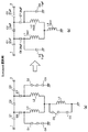
図1は本実施の形態に係る帯域可変フィルタの回路構成図である。同図に示す帯域可変フィルタは、入力端子1に対してアンテナ側から高周波信号が導入され、出力端子2から当該フィルタで抽出した所望帯域の高周波信号が出力される。この入力端子1と出力端子2との間に第1、第2、第3のコンデンサC1,C2,C3が直列に接続されている。第1のコンデンサC1と第2のコンデンサC2との接続点に第1のインダクタL1の一端が接続されている。第1のインダクタL1の一端とグラウンドとの間に第4のコンデンサC4が接続され、当該第4のコンデンサC4と第1のインダクタL1の一端との間に第1のPINダイオードD1が接続されている。また、第2のインダクタL2の一端とグラウンドとの間に第5のコンデンサC5が接続され、当該第5のコンデンサC5と第2のインダクタL1の一端との間に第2のPINダイオードD2が接続されている。
FIG. 1 is a circuit configuration diagram of a variable band filter according to the present embodiment. In the variable band filter shown in FIG. 1, a high frequency signal is introduced from the antenna side to the
本実施の形態では、第1のコンデンサC1と第2のコンデンサC2の接続点と第1のインダクタL1の一端との間に第6のコンデンサC6が接続され、第2のコンデンサC2と第3のコンデンサC3の接続点と第2のインダクタL2の一端との間に第7のコンデンサC7接続されている。 In the present embodiment, a sixth capacitor C6 is connected between the connection point of the first capacitor C1 and the second capacitor C2 and one end of the first inductor L1, and the second capacitor C2 and the third capacitor C2 are connected to each other. A seventh capacitor C7 is connected between the connection point of the capacitor C3 and one end of the second inductor L2.
また、第1及び第2のインダクタL1,L2の他端が第3のインダクタL3の一端に接続され、第3のインダクタL3の他端がグラウンドに接続されている。第3のインダクタL3と並列に直流カット用の第8のコンデンサC8が接続され、第8のコンデンサC8と第3のインダクタL3の一端との間に第3のPINダイオードD3が接続されている。 The other ends of the first and second inductors L1 and L2 are connected to one end of the third inductor L3, and the other end of the third inductor L3 is connected to the ground. An eighth capacitor C8 for direct current cut is connected in parallel with the third inductor L3, and a third PIN diode D3 is connected between the eighth capacitor C8 and one end of the third inductor L3.
また、ハイバンド(UHF放送帯域)とローバンド(VHF放送帯域)を切替える切替え回路3を備えている。切替え回路3の固定端は電源4に接続され、一方の切替え端子3aは第3のPINダイオードD3のアノードに接続され、他方の切替え端子3bは第1及び第2のPINダイオードD1,D2のアノードに接続されている。切替え回路3において、固定端を切替え端子3aに接続するとハイバンドが選択され、固定端を切替え端子3bに接続するとローバンドが選択されるように構成している。
In addition, a
次に、以上のように構成された本実施の形態に係る帯域可変フィルタの動作及び設定されるフィルタ特性について説明する。
最初に、切替え回路3において固定端を切替え端子3bに接続してローバンド(VHF放送帯域)を選択した場合について説明する。図2(a)はローバンド選択における第1、第2、第3のPINダイオードD1,D2,D3のオン/オフ状態を示している。切替え回路3を介して第1及び第2のPINダイオードD1,D2のアノードに電圧が印加されて、第1及び第2のPINダイオードD1,D2がオンする。これにより、第1、第2のインダクタL1,L2の一端は、第4、第5のコンデンサC4,C5を介してグラウンドに接続される。また、第3のPINダイオードD3のアノードは0Vとなってオフするので、第3のインダクタL3に対して第8のコンデンサC8は並列接続されなくなる。
Next, the operation of the variable band filter according to the present embodiment configured as described above and the set filter characteristics will be described.
First, the case where the low end (VHF broadcast band) is selected by connecting the fixed end to the
図2(b)は、第1、第2、第3のPINダイオードD1,D2,D3を図2(a)に示すように設定した状態の等価回路図である。第1のインダクタL1及び第3のインダクタL3と第6のコンデンサC6及び第4のコンデンサC4とからLC共振回路が構成されると共に、第2のインダクタL2及び第3のインダクタL3と第7のコンデンサC7及び第5のコンデンサC5とからLC共振回路が構成される。そして、2つの共振回路が第3のインダクタL3でM結合されて、トラップを有する複同調回路が構成される。 FIG. 2B is an equivalent circuit diagram in a state where the first, second, and third PIN diodes D1, D2, and D3 are set as shown in FIG. The first inductor L1, the third inductor L3, the sixth capacitor C6, and the fourth capacitor C4 constitute an LC resonance circuit, and the second inductor L2, the third inductor L3, and the seventh capacitor. The LC resonance circuit is configured by C7 and the fifth capacitor C5. Then, the two resonant circuits are M-coupled by the third inductor L3, thereby forming a double-tuned circuit having a trap.
図3は、複同調回路を構成する各構成要素に図2(b)に示す数値を設定してシミュレーションした周波数特性図である。同図に示すように、VHF放送帯域の減衰が極めて小さく、しかもVHF放送帯域の低域側の隣接領域が30dB程度減衰する一方、VHF放送帯域の高域側の隣接領域が10dB程度減衰しており、VHF放送帯域を通過帯域とするバンドパスフィルタ特性が得られていることが判る。しかも、FM帯域にトラップが形成されており、テレビジョンチューナにおいて妨害波となるFM帯域を十分に減衰させることができる。 FIG. 3 is a frequency characteristic diagram that is simulated by setting the numerical values shown in FIG. 2B to the respective components constituting the double-tuned circuit. As shown in the figure, the attenuation of the VHF broadcasting band is extremely small, and the adjacent area on the low side of the VHF broadcasting band is attenuated by about 30 dB, while the adjacent area on the high side of the VHF broadcasting band is attenuated by about 10 dB. Thus, it can be seen that bandpass filter characteristics having a VHF broadcast band as a pass band are obtained. In addition, traps are formed in the FM band, and the FM band that becomes an interference wave in the television tuner can be sufficiently attenuated.
次に、切替え回路3において固定端を切替え端子3aに接続してハイバンド(UHF放送帯域)を選択した場合について説明する。図4(a)はハイバンド選択時における第1、第2、第3のPINダイオードD1,D2,D3のオン/オフ状態を示している。切替え回路3を介して第3のPINダイオードD3のアノードに電圧が印加されて、第3のPINダイオードD3がオンする。これにより、第3のインダクタL3に対して第8のコンデンサC8が並列に接続される。また、第1、第2のPINダイオードD1,D2のアノードは0Vとなってオフするので、第1、第2のインダクタL1,L2に対して第4、第5のコンデンサC4、C8は並列接続されなくなる。
Next, the case where the high band (UHF broadcast band) is selected by connecting the fixed end to the switching terminal 3a in the
図4(b)は、第1、第2、第3のPINダイオードD1,D2,D3を図4(a)に示すように設定した状態の等価回路図である。第1のコンデンサC1と第2のコンデンサC2との接続点が第6のコンデンサC6及び第1のインダクタL1を介してグラウンドに接続され、第2のコンデンサC2と第3のコンデンサC3との接続点が第7のコンデンサC7及び第2のインダクタL2を介してグラウンドに接続され、全体でπ型のハイパスフィルタが形成されている。 FIG. 4B is an equivalent circuit diagram in a state where the first, second, and third PIN diodes D1, D2, and D3 are set as shown in FIG. 4A. A connection point between the first capacitor C1 and the second capacitor C2 is connected to the ground via the sixth capacitor C6 and the first inductor L1, and a connection point between the second capacitor C2 and the third capacitor C3. Are connected to the ground via the seventh capacitor C7 and the second inductor L2, and a π-type high-pass filter is formed as a whole.
図5は、π型のハイパスフィルタを構成する各構成要素に図4(b)に示す数値を設定してシミュレーションした周波数特性図である。同図に示すように、UHF放送帯域及びそれ以上の帯域では減衰がほとんど無く、UHF放送帯域の低域側の端部において300MHzに向けて30dB近く減衰しており、所望のハイパスフィルタ特性が得られている。また、特定小電力無線帯域(322MHz)及びアナログコードレス電話親機の使用帯域(330MHz)にトラップが形成されている。 FIG. 5 is a frequency characteristic diagram that is simulated by setting the numerical values shown in FIG. 4B to the constituent elements of the π-type high-pass filter. As shown in the figure, there is almost no attenuation in the UHF broadcast band and higher bands, and it is attenuated by about 30 dB toward 300 MHz at the lower end of the UHF broadcast band, and a desired high-pass filter characteristic is obtained. It has been. In addition, traps are formed in the specific low-power radio band (322 MHz) and the use band (330 MHz) of the analog cordless telephone master unit.
このように本実施の形態によれば、VHF放送帯域を通過帯域とするバンドパスフィルタと、UHF放送帯域を通過帯域とするハイパスフィルタとを並列に設けることなく、VHF放送帯域とUHF放送帯域を選択可能な高周波フィルタを実現することができ、部品点数の削減による小型化とコストダウンを図ることができる。また、VHF放送帯域選択時にはFM帯域及びUHF放送帯域の双方を減衰させるバンドパスフィルタと、UHF放送帯域選択時にはFM帯域及びVHF放送帯域を含む帯域を減衰させるハイパスフィルタとを、第1、第2、第3のPINダイオードD1,D2,D3で切替えることができ、ダイオードの部品数を削減することもできる。 As described above, according to the present embodiment, the VHF broadcast band and the UHF broadcast band are set in parallel without providing a bandpass filter having the VHF broadcast band as a pass band and a high-pass filter having the UHF broadcast band as the pass band. A selectable high-frequency filter can be realized, and the size and cost can be reduced by reducing the number of components. A first and second bandpass filter that attenuates both the FM band and the UHF broadcast band when the VHF broadcast band is selected, and a highpass filter that attenuates a band including the FM band and the VHF broadcast band when the UHF broadcast band is selected. The third PIN diodes D1, D2, and D3 can be switched, and the number of diode components can be reduced.
なお、VHF放送帯域選択時のFM帯域の減衰や、UHF放送帯域選択時の特定小電力無線帯域及びアナログコードレス電話親機の使用帯域(322〜330MHz付近)の減衰が小さくても問題とならないのであれば、第6及び第7のコンデンサC6,C7を削除することも可能である。 Note that there is no problem even if the attenuation of the FM band at the time of selecting the VHF broadcasting band, or the attenuation of the specific low power wireless band and the band used for the analog cordless telephone base unit (around 322 to 330 MHz) at the time of selecting the UHF broadcasting band is not a problem. If so, the sixth and seventh capacitors C6 and C7 can be deleted.
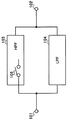
図6は第6及び第7のコンデンサC6,C7(24pF)を削除した帯域可変フィルタの構成図である。なお、切替え回路3の代わりに、ハイ/ローが逆になる2電源5a,5bを用いている。帯域可変フィルタを構成する各構成要素の数値は上記実施の形態と同様である。
FIG. 6 is a configuration diagram of a band-variable filter in which the sixth and seventh capacitors C6 and C7 (24 pF) are omitted. Instead of the
図7(a)は図6の帯域可変フィルタで第1、第2のPINダイオードD1,D2をオン(電源5b=H)、第3のPINダイオードD3をオフ(電源5a=L)として、ローバンド選択した場合の周波数特性図である。同図に示すように、VHF放送帯域を通過帯域とするバンドパスフィルタ特性を示している。但し、FM帯域にトラップは形成されていない。
FIG. 7A shows a low-band filter in which the first and second PIN diodes D1 and D2 are turned on (
図7(b)は図6の帯域可変フィルタで第1、第2のPINダイオードD1,D2をオフ(電源5b=L)、第3のPINダイオードD3をオン(電源5a=H)としてハイバンド選択した場合の周波数特性図である。同図に示すように、UHF放送帯域以上を通過帯域とするハイパスフィルタ特性を示している。但し、特定小電力無線帯域及びアナログコードレス電話親機の使用帯域(322〜330MHz付近)で十分な減衰となっていない。
FIG. 7B is a band-variable filter of FIG. 6 in which the first and second PIN diodes D1 and D2 are turned off (
このように、第6及び第7のコンデンサC6,C7を削除しても、VHF放送帯域を通過帯域とするバンドパスフィルタと、UHF放送帯域を通過帯域とするハイパスフィルタとを並列に設けることなく、VHF放送帯域とUHF放送帯域を選択可能な高周波フィルタを実現することができる。 In this way, even if the sixth and seventh capacitors C6 and C7 are deleted, a bandpass filter having a VHF broadcast band as a passband and a highpass filter having a UHF broadcast band as a passband are not provided in parallel. A high frequency filter capable of selecting a VHF broadcast band and a UHF broadcast band can be realized.
なお、本発明は上記一実施の形態に限定されるものではなく、本発明の要旨を逸脱しない範囲で種々変形実施可能である。例えば、第1、第2、第3のスイッチは、PINダイオードに限定されず、その他のスイッチ部品を用いることもできる。また、第1、第2、第3のPINダイオードD1、D2、D3と、第4、第5、第8のコンデンサC4,C5,C8との位置関係を逆にしても良い。 The present invention is not limited to the above-described embodiment, and various modifications can be made without departing from the gist of the present invention. For example, the first, second, and third switches are not limited to PIN diodes, and other switch components can be used. Further, the positional relationship between the first, second, and third PIN diodes D1, D2, and D3 and the fourth, fifth, and eighth capacitors C4, C5, and C8 may be reversed.
また、上述した周波数特性のシミュレーションンには、日本でのVHF放送帯域及びUHF放送帯域に基づいて最適化した数値を設定しているが、用途、目的に応じて適宜最適化した数値を設定することができる。また、バンドパスフィルタとハイパスフィルタとを切替える用途であれば、テレビジョンチューナの高周波フィルタ以外にも適用可能である。 In the above-described frequency characteristic simulation, optimized values are set based on the VHF broadcast band and UHF broadcast band in Japan. However, appropriately optimized values are set according to the application and purpose. be able to. Further, as long as the bandpass filter and the highpass filter are switched, the present invention can be applied to other than the high frequency filter of the television tuner.
本発明は、バンドパスフィルタとハイパスフィルタとを切替える高周波フィルタに適用可能である。 The present invention is applicable to a high-frequency filter that switches between a band-pass filter and a high-pass filter.
1…入力端子
2…出力端子
C1〜C8…第1〜第8のコンデンサ
D1〜D3…第1〜第3のPINダイオード
L1、L2…第1、第2のインダクタ
3…切替え回路
4…電源
DESCRIPTION OF
Claims (5)
前記第1のコンデンサの他端に一端が接続された第2のコンデンサと、
前記第2のコンデンサの他端と出力端子との間に接続された第3のコンデンサと、
前記第1のコンデンサと前記第2のコンデンサとの接続点に一端が接続された第1のインダクタと、
一端がグラウンドに接続された第4のコンデンサと、
前記第4のコンデンサの他端を前記第1のインダクタの一端に対して接続し又は非接続とする第1のスイッチと、
前記第2のコンデンサと前記第3のコンデンサとの接続点に一端が接続された第2のインダクタと、
一端がグラウンドに接続された第5のコンデンサと、
前記第5のコンデンサの他端を前記第2のインダクタの一端に対して接続し又は非接続とする第2のスイッチと、
前記第1のインダクタの他端及び前記第2のインダクタの他端とグラウンドとの間に接続される第3のインダクタと、
前記第3のインダクタと並列に接続され、前記第3のインダクタの両端を高周波的に短絡する第3のスイッチと、を備え、
前記第1及び第2のスイッチをオンにすると共に前記第3のスイッチをオフにして、帯域通過フィルタを形成し、前記第1及び第2のスイッチをオフにすると共に前記第3のスイッチをオンにして、前記帯域通過フィルタよりも通過帯域が高い高域通過フィルタを形成する帯域可変フィルタ。 A first capacitor having one end connected to the input terminal;
A second capacitor having one end connected to the other end of the first capacitor;
A third capacitor connected between the other end of the second capacitor and the output terminal;
A first inductor having one end connected to a connection point between the first capacitor and the second capacitor;
A fourth capacitor with one end connected to ground ;
A first switch for connecting or disconnecting the other end of the fourth capacitor to one end of the first inductor;
A second inductor having one end connected to a connection point between the second capacitor and the third capacitor;
A fifth capacitor with one end connected to ground ;
A second switch for connecting or disconnecting the other end of the fifth capacitor to one end of the second inductor;
A third inductor connected between the other end of the first inductor and the other end of the second inductor and the ground;
A third switch connected in parallel with the third inductor and short-circuiting both ends of the third inductor at a high frequency,
Turning on the first and second switches and turning off the third switch to form a band-pass filter, turning off the first and second switches and turning on the third switch A band-variable filter that forms a high-pass filter having a higher pass band than the band-pass filter.
前記第2及び第3のコンデンサの接続点と前記第2のインダクタの一端との間に接続された第7のコンデンサと、を備え、
前記第1及び第2のスイッチをオンにすると共に前記第3のスイッチをオフにして、帯域通過フィルタを形成した際に、当該帯域通過フィルタの通過帯域よりも低い周波数に減衰極のあるトラップ回路が形成され、
前記第1及び第2のスイッチをオフにすると共に前記第3のスイッチをオンにして、前記帯域通過フィルタよりも通過帯域が高い高域通過フィルタを形成した際に、当該高域通過フィルタの通過帯域よりも低い周波数に減衰極のあるトラップ回路が形成される、
ことを特徴とする請求項1記載の帯域可変フィルタ。 A sixth capacitor connected between a connection point of the first and second capacitors and one end of the first inductor;
A seventh capacitor connected between a connection point of the second and third capacitors and one end of the second inductor;
When the first and second switches are turned on and the third switch is turned off to form a band pass filter, a trap circuit having an attenuation pole at a frequency lower than the pass band of the band pass filter Formed,
When the first and second switches are turned off and the third switch is turned on to form a high-pass filter having a higher pass band than the band-pass filter, the high-pass filter passes therethrough. A trap circuit with an attenuation pole at a frequency lower than the band is formed.
The band-variable filter according to claim 1.
前記第1のスイッチダイオードは、そのアノードに前記第4のコンデンサが接続され、そのカソードに前記第1のインダクタの一端が接続され、
前記第2のスイッチダイオードは、そのアノードに前記第5のコンデンサが接続され、そのカソードに前記第2のインダクタの一端が接続され、
前記第1及び第2のスイッチダイオードのアノードに制御電圧が印加されることを特徴とする請求項1又は請求項2記載の帯域可変フィルタ。 The first and second switches are respectively composed of first and second switch diodes composed of diodes,
The first switch diode has an anode connected to the fourth capacitor, and a cathode connected to one end of the first inductor.
The second switch diode has the anode connected to the fifth capacitor, and the cathode connected to one end of the second inductor.
3. The band variable filter according to claim 1, wherein a control voltage is applied to anodes of the first and second switch diodes.
前記第3のスイッチダイオードは、そのカソードに前記第1、第2、第3のインダクタの接続点が接続され、
前記第8のコンデンサの一端がグラウンドに接続され、
前記第3のスイッチダイオードのアノードに制御電圧が印加されることを特徴とする請求項1から請求項3の何れかに記載の帯域可変フィルタ。 The third switch is composed of a third switch diode made of a diode, and an eighth capacitor for DC cut whose one end is connected to the anode of the third switch diode.
The third switch diode has a cathode connected to a connection point of the first, second, and third inductors,
One end of the eighth capacitor is connected to ground,
The band-variable filter according to any one of claims 1 to 3, wherein a control voltage is applied to an anode of the third switch diode.
前記第1及び第2のスイッチをオフにすると共に前記第3のスイッチをオンにした場合の通過帯域がUHF帯以上であることを特徴とする請求項1から請求項4の何れかに記載の帯域可変フィルタ。 When the first and second switches are turned on and the third switch is turned off, the pass band is a VHF broadcast band,
5. The passband when the first and second switches are turned off and the third switch is turned on is equal to or higher than the UHF band. 6. Band-variable filter.
Priority Applications (3)
| Application Number | Priority Date | Filing Date | Title |
|---|---|---|---|
| JP2007060472A JP4713523B2 (en) | 2007-03-09 | 2007-03-09 | Bandwidth variable filter |
| TW97106641A TW200901623A (en) | 2007-03-09 | 2008-02-26 | Alterable band-pass filter |
| CN200810082192XA CN101262209B (en) | 2007-03-09 | 2008-03-07 | Alterable band-pass filter |
Applications Claiming Priority (1)
| Application Number | Priority Date | Filing Date | Title |
|---|---|---|---|
| JP2007060472A JP4713523B2 (en) | 2007-03-09 | 2007-03-09 | Bandwidth variable filter |
Publications (2)
| Publication Number | Publication Date |
|---|---|
| JP2008227729A JP2008227729A (en) | 2008-09-25 |
| JP4713523B2 true JP4713523B2 (en) | 2011-06-29 |
Family
ID=39845839
Family Applications (1)
| Application Number | Title | Priority Date | Filing Date |
|---|---|---|---|
| JP2007060472A Active JP4713523B2 (en) | 2007-03-09 | 2007-03-09 | Bandwidth variable filter |
Country Status (3)
| Country | Link |
|---|---|
| JP (1) | JP4713523B2 (en) |
| CN (1) | CN101262209B (en) |
| TW (1) | TW200901623A (en) |
Families Citing this family (4)
| Publication number | Priority date | Publication date | Assignee | Title |
|---|---|---|---|---|
| TWI470928B (en) | 2009-09-02 | 2015-01-21 | Mstar Semiconductor Inc | Tuner and its front-end circuit |
| CN103795939A (en) * | 2014-01-22 | 2014-05-14 | 中国科学院长春光学精密机械与物理研究所 | Sampling system using variable band pass filter and double- correlation sampling method |
| CN108028635B (en) | 2015-09-09 | 2021-04-20 | 株式会社村田制作所 | Variable-frequency LC filter and high-frequency front-end circuit |
| CN113014222B (en) * | 2021-04-26 | 2023-08-08 | 哈尔滨海能达科技有限公司 | Band-pass filter circuit and electronic equipment |
Citations (5)
| Publication number | Priority date | Publication date | Assignee | Title |
|---|---|---|---|---|
| JPS56103514A (en) * | 1980-01-23 | 1981-08-18 | Hitachi Ltd | Filter circuit |
| JPS61239727A (en) * | 1985-04-17 | 1986-10-25 | Hitachi Ltd | Input circuit of tuner |
| JPH06334463A (en) * | 1993-05-26 | 1994-12-02 | Toshiba Corp | Band changeover circuit |
| JPH07321586A (en) * | 1994-05-20 | 1995-12-08 | Kokusai Electric Co Ltd | Variable frequency band filter |
| JP2002009504A (en) * | 2000-04-19 | 2002-01-11 | Murata Mfg Co Ltd | Frequency variable filter, antenna multicoupler and communication unit |
-
2007
- 2007-03-09 JP JP2007060472A patent/JP4713523B2/en active Active
-
2008
- 2008-02-26 TW TW97106641A patent/TW200901623A/en unknown
- 2008-03-07 CN CN200810082192XA patent/CN101262209B/en not_active Expired - Fee Related
Patent Citations (5)
| Publication number | Priority date | Publication date | Assignee | Title |
|---|---|---|---|---|
| JPS56103514A (en) * | 1980-01-23 | 1981-08-18 | Hitachi Ltd | Filter circuit |
| JPS61239727A (en) * | 1985-04-17 | 1986-10-25 | Hitachi Ltd | Input circuit of tuner |
| JPH06334463A (en) * | 1993-05-26 | 1994-12-02 | Toshiba Corp | Band changeover circuit |
| JPH07321586A (en) * | 1994-05-20 | 1995-12-08 | Kokusai Electric Co Ltd | Variable frequency band filter |
| JP2002009504A (en) * | 2000-04-19 | 2002-01-11 | Murata Mfg Co Ltd | Frequency variable filter, antenna multicoupler and communication unit |
Also Published As
| Publication number | Publication date |
|---|---|
| JP2008227729A (en) | 2008-09-25 |
| CN101262209A (en) | 2008-09-10 |
| CN101262209B (en) | 2010-06-16 |
| TW200901623A (en) | 2009-01-01 |
| TWI342669B (en) | 2011-05-21 |
Similar Documents
| Publication | Publication Date | Title |
|---|---|---|
| US10200012B2 (en) | High-frequency filter, front-end circuit, and communication apparatus | |
| US9979375B2 (en) | Multi-harmonic matching networks | |
| CN108899158B (en) | Tunable inductor arrangement, transceiver, method and computer program | |
| JP4713523B2 (en) | Bandwidth variable filter | |
| WO2002054591A1 (en) | High frequency low-pass filter | |
| CN101197976B (en) | Variable tuning circuit using variable capacitance diode and television tuner | |
| US6472957B1 (en) | Low power switchable filter tuner | |
| EP2091151A1 (en) | Television tuner | |
| JP3614614B2 (en) | Television signal receiving tuner | |
| JP2001223954A (en) | Input circuit for television tuner | |
| JP5467815B2 (en) | High frequency switch circuit | |
| JP3103017U (en) | Television tuner | |
| JP2011019168A (en) | Reception tuner | |
| KR101640400B1 (en) | Brodband tunable band-pass filter | |
| JP2010154232A (en) | Frequency variable filter circuit | |
| JP4043222B2 (en) | Television tuner | |
| EP1337042A1 (en) | Television tuner | |
| JP3050884B2 (en) | Electronic tuner input circuit | |
| JP3801845B2 (en) | Television tuner | |
| KR100274047B1 (en) | TV signal input circuit | |
| JP2001359005A (en) | Tuner for receiving television signal | |
| JP2005064780A (en) | High frequency switching circuit | |
| JP2010136175A (en) | Filter circuit | |
| KR20060081138A (en) | Frequency selecting type tuner | |
| JP2002246932A (en) | Television tuner |
Legal Events
| Date | Code | Title | Description |
|---|---|---|---|
| A621 | Written request for application examination |
Free format text: JAPANESE INTERMEDIATE CODE: A621 Effective date: 20091026 |
|
| A521 | Written amendment |
Free format text: JAPANESE INTERMEDIATE CODE: A523 Effective date: 20100611 |
|
| A977 | Report on retrieval |
Free format text: JAPANESE INTERMEDIATE CODE: A971007 Effective date: 20101206 |
|
| A131 | Notification of reasons for refusal |
Free format text: JAPANESE INTERMEDIATE CODE: A131 Effective date: 20101221 |
|
| A521 | Written amendment |
Free format text: JAPANESE INTERMEDIATE CODE: A523 Effective date: 20110131 |
|
| A01 | Written decision to grant a patent or to grant a registration (utility model) |
Free format text: JAPANESE INTERMEDIATE CODE: A01 Effective date: 20110308 |
|
| A61 | First payment of annual fees (during grant procedure) |
Free format text: JAPANESE INTERMEDIATE CODE: A61 Effective date: 20110324 |
|
| S533 | Written request for registration of change of name |
Free format text: JAPANESE INTERMEDIATE CODE: R313533 |
|
| R350 | Written notification of registration of transfer |
Free format text: JAPANESE INTERMEDIATE CODE: R350 |