JP4688068B2 - Antenna device - Google Patents
Antenna device Download PDFInfo
- Publication number
- JP4688068B2 JP4688068B2 JP2006180513A JP2006180513A JP4688068B2 JP 4688068 B2 JP4688068 B2 JP 4688068B2 JP 2006180513 A JP2006180513 A JP 2006180513A JP 2006180513 A JP2006180513 A JP 2006180513A JP 4688068 B2 JP4688068 B2 JP 4688068B2
- Authority
- JP
- Japan
- Prior art keywords
- ground
- substrate
- antenna
- ground conductor
- conductor
- Prior art date
- Legal status (The legal status is an assumption and is not a legal conclusion. Google has not performed a legal analysis and makes no representation as to the accuracy of the status listed.)
- Expired - Fee Related
Links
- 239000004020 conductor Substances 0.000 claims description 78
- 239000000758 substrate Substances 0.000 claims description 65
- 238000004891 communication Methods 0.000 description 5
- 239000003989 dielectric material Substances 0.000 description 4
- 230000000694 effects Effects 0.000 description 4
- 238000004088 simulation Methods 0.000 description 4
- PNEYBMLMFCGWSK-UHFFFAOYSA-N aluminium oxide Inorganic materials [O-2].[O-2].[O-2].[Al+3].[Al+3] PNEYBMLMFCGWSK-UHFFFAOYSA-N 0.000 description 3
- 239000000696 magnetic material Substances 0.000 description 3
- 239000002184 metal Substances 0.000 description 3
- 229910052751 metal Inorganic materials 0.000 description 3
- 230000005855 radiation Effects 0.000 description 3
- 238000004364 calculation method Methods 0.000 description 2
- RYGMFSIKBFXOCR-UHFFFAOYSA-N Copper Chemical compound [Cu] RYGMFSIKBFXOCR-UHFFFAOYSA-N 0.000 description 1
- 239000002390 adhesive tape Substances 0.000 description 1
- 239000003990 capacitor Substances 0.000 description 1
- 239000002131 composite material Substances 0.000 description 1
- 238000012790 confirmation Methods 0.000 description 1
- 239000000470 constituent Substances 0.000 description 1
- 239000011889 copper foil Substances 0.000 description 1
- 238000010586 diagram Methods 0.000 description 1
- 238000005516 engineering process Methods 0.000 description 1
- 238000011156 evaluation Methods 0.000 description 1
- 239000011810 insulating material Substances 0.000 description 1
- 239000000463 material Substances 0.000 description 1
- 238000000034 method Methods 0.000 description 1
- 239000011347 resin Substances 0.000 description 1
- 229920005989 resin Polymers 0.000 description 1
Images


Classifications
-
- H—ELECTRICITY
- H01—ELECTRIC ELEMENTS
- H01Q—ANTENNAS, i.e. RADIO AERIALS
- H01Q1/00—Details of, or arrangements associated with, antennas
- H01Q1/12—Supports; Mounting means
- H01Q1/22—Supports; Mounting means by structural association with other equipment or articles
- H01Q1/24—Supports; Mounting means by structural association with other equipment or articles with receiving set
- H01Q1/241—Supports; Mounting means by structural association with other equipment or articles with receiving set used in mobile communications, e.g. GSM
- H01Q1/242—Supports; Mounting means by structural association with other equipment or articles with receiving set used in mobile communications, e.g. GSM specially adapted for hand-held use
- H01Q1/243—Supports; Mounting means by structural association with other equipment or articles with receiving set used in mobile communications, e.g. GSM specially adapted for hand-held use with built-in antennas
-
- H—ELECTRICITY
- H01—ELECTRIC ELEMENTS
- H01Q—ANTENNAS, i.e. RADIO AERIALS
- H01Q1/00—Details of, or arrangements associated with, antennas
- H01Q1/12—Supports; Mounting means
- H01Q1/22—Supports; Mounting means by structural association with other equipment or articles
- H01Q1/24—Supports; Mounting means by structural association with other equipment or articles with receiving set
-
- H—ELECTRICITY
- H01—ELECTRIC ELEMENTS
- H01Q—ANTENNAS, i.e. RADIO AERIALS
- H01Q1/00—Details of, or arrangements associated with, antennas
- H01Q1/36—Structural form of radiating elements, e.g. cone, spiral, umbrella; Particular materials used therewith
- H01Q1/362—Structural form of radiating elements, e.g. cone, spiral, umbrella; Particular materials used therewith for broadside radiating helical antennas
-
- H—ELECTRICITY
- H01—ELECTRIC ELEMENTS
- H01Q—ANTENNAS, i.e. RADIO AERIALS
- H01Q1/00—Details of, or arrangements associated with, antennas
- H01Q1/36—Structural form of radiating elements, e.g. cone, spiral, umbrella; Particular materials used therewith
- H01Q1/38—Structural form of radiating elements, e.g. cone, spiral, umbrella; Particular materials used therewith formed by a conductive layer on an insulating support
-
- H—ELECTRICITY
- H01—ELECTRIC ELEMENTS
- H01Q—ANTENNAS, i.e. RADIO AERIALS
- H01Q1/00—Details of, or arrangements associated with, antennas
- H01Q1/48—Earthing means; Earth screens; Counterpoises
-
- H—ELECTRICITY
- H01—ELECTRIC ELEMENTS
- H01Q—ANTENNAS, i.e. RADIO AERIALS
- H01Q9/00—Electrically-short antennas having dimensions not more than twice the operating wavelength and consisting of conductive active radiating elements
- H01Q9/04—Resonant antennas
- H01Q9/30—Resonant antennas with feed to end of elongated active element, e.g. unipole
- H01Q9/40—Element having extended radiating surface
Landscapes
- Engineering & Computer Science (AREA)
- Computer Networks & Wireless Communication (AREA)
- Details Of Aerials (AREA)
- Support Of Aerials (AREA)
Description
本発明は、無線通信機器の小型化に適したアンテナ装置に関する。 The present invention relates to an antenna device suitable for miniaturization of a wireless communication device.
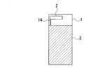
携帯電話機や無線通信機能内蔵のノート型パーソナルコンピュータ等の無線通信機器では、その小型化に伴って部品実装密度も高くなってきている。この対策として、例えば、特許文献1には、誘電体又は磁性体からなる基体表面に螺旋導体層を形成した、いわゆるチップアンテナを基板上に設置し、基板上に形成したグラウンド面にチップアンテナを接地させた技術が開示されている。この場合、例えば、図5に示すように、基板1上のチップアンテナ2が接地されるRFグラウンド導体3は、充分なアンテナ特性を得るために理想的には基板1上の大部分の面積を必要とする。
In wireless communication devices such as mobile phones and notebook personal computers with a built-in wireless communication function, the component mounting density is increasing with the miniaturization. As a countermeasure, for example, in Patent Document 1, a so-called chip antenna in which a spiral conductor layer is formed on the surface of a base made of a dielectric material or a magnetic material is installed on a substrate, and the chip antenna is mounted on a ground surface formed on the substrate. A grounded technique is disclosed. In this case, for example, as shown in FIG. 5, the
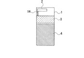
また、近年、無線通信機器のデジタル化に伴って、図6に示すように、チップアンテナ2が接地されるRFグラウンド導体3と共にデジタル回路用グラウンドとなる回路用グラウンド導体4を基板1上に形成して、RFグラウンド導体3と回路用グラウンド導体4とを同一基板1上に共存させることも検討されている。
In recent years, with the digitization of wireless communication devices, as shown in FIG. 6, a circuit ground conductor 4 serving as a digital circuit ground is formed on the substrate 1 together with an
しかしながら、上記従来の技術には、以下の課題が残されている。
すなわち、アンテナエレメントの電気長が1/4波長(λ)である1/4波長型アンテナでは、アンテナが接地されるグラウンド面の大きさ(特に長さ)が重要であるが、部品実装の高密度に伴ってアンテナ特性を得るために必要なグラウンド面積を、図5に示すような理想的な状態で充分に確保することが困難になってきている。
また、図6に示すように、同一基板1上にRFグラウンド導体3と回路用グラウンド導体4とが共存する場合、基板1上のグラウンド面が分割され、RFグラウンド導体3の必要な面積が確保できない不都合があった。
However, the following problems remain in the conventional technology.
In other words, in a quarter wavelength antenna in which the electrical length of the antenna element is a quarter wavelength (λ), the size (particularly the length) of the ground surface on which the antenna is grounded is important. As the density increases, it has become difficult to sufficiently secure a ground area necessary for obtaining antenna characteristics in an ideal state as shown in FIG.
In addition, as shown in FIG. 6, when the
本発明は、前述の課題に鑑みてなされたもので、基板上でRFグラウンド導体を広く形成した場合と同様なアンテナ特性を得ることができ、同一基板上で回路用グラウンド導体との共存も可能なアンテナ装置を提供することを目的とする。 The present invention has been made in view of the above-described problems, and can obtain the same antenna characteristics as when a wide RF ground conductor is formed on a substrate, and can coexist with a circuit ground conductor on the same substrate. It is an object to provide a simple antenna device.
本発明は、前記課題を解決するために以下の構成を採用した。すなわち、本発明のアンテナ装置は、基板と、該基板上の表面に少なくとも一部が形成されアンテナ接地グラウンドとなるRFグラウンド導体と、前記RFグラウンド導体に一端が接続されたアンテナ部とを備え、前記RFグラウンド導体が、少なくとも2方向に分岐して延在していることを特徴とする。 The present invention employs the following configuration in order to solve the above problems. That is, the antenna device of the present invention includes a substrate, an RF ground conductor that is at least partially formed on the surface of the substrate and serving as an antenna ground ground, and an antenna portion that has one end connected to the RF ground conductor. The RF ground conductor is branched and extended in at least two directions.
このアンテナ装置では、RFグラウンド導体が、少なくとも2方向に分岐して延在しているので、全体のグラウンド面積は少ないが2方向に延びてアンテナ特性に必要な長さを確保することで、一つの大面積のグラウンドと同様の放射効率が得られ、充分なアンテナ特性を有することが可能になる。 In this antenna device, since the RF ground conductor extends in at least two directions and extends, the entire ground area is small, but it extends in two directions to ensure a length necessary for antenna characteristics. Radiation efficiency similar to that of one large-area ground can be obtained, and sufficient antenna characteristics can be obtained.
また、本発明のアンテナ装置は、前記RFグラウンド導体が、互いに直交する方向に分岐した逆L字状に形成されていることを特徴とする。すなわち、このアンテナ装置では、逆L字状に分岐したRFグラウンド導体を有しているので、矩形状の基板を用いた際に、基板の短辺及び長辺に沿ってRFグラウンド導体を配することで、基板表面を有効に用いることができる。また、RFグラウンド導体が互いに直交する方向に分岐していることで、全方向的にアンテナ特性に寄与することができる。 In the antenna device of the present invention, the RF ground conductor is formed in an inverted L shape that branches in directions orthogonal to each other. That is, since this antenna device has an RF ground conductor branched in an inverted L shape, when a rectangular substrate is used, the RF ground conductor is arranged along the short side and the long side of the substrate. Thus, the substrate surface can be used effectively. Further, since the RF ground conductors are branched in directions orthogonal to each other, it is possible to contribute to antenna characteristics in all directions.
また、本発明のアンテナ装置は、前記アンテナ部が、前記基板上に設置されたチップアンテナであり、前記RFグラウンド導体が、前記チップアンテナに沿って延在する第1グラウンド部と、前記第1グラウンド部の延在方向に対して直交する方向にかつ前記第1グラウンドから前記チップアンテナから離間する方向に延在する第2グラウンド部とを前記基板上に有していることを特徴とする。すなわち、このアンテナ装置では、チップアンテナに沿った第1グラウンド部とチップアンテナに垂直な第2グラウンド部とからRFグラウンド導体が構成されるので、チップアンテナとの上記配置関係で小さなスペースでも良好なアンテナ特性を得ることができる。 In the antenna device of the present invention, the antenna unit is a chip antenna installed on the substrate, the RF ground conductor extends along the chip antenna, and the first The substrate has a second ground portion extending on the substrate in a direction orthogonal to the extending direction of the ground portion and in a direction away from the chip antenna from the first ground. That is, in this antenna device, since the RF ground conductor is composed of the first ground portion along the chip antenna and the second ground portion perpendicular to the chip antenna, the above-described arrangement relationship with the chip antenna is good even in a small space. Antenna characteristics can be obtained.
また、本発明のアンテナ装置は、前記RFグラウンド導体が、前記基板上に形成された基板グラウンド部と、前記基板グラウンド部に基端が接続され前記基板グラウンド部と異なる方向であって前記基板の外部に延在する外部グラウンド部とで構成されていることを特徴とする。すなわち、このアンテナ装置では、基板グラウンド部と外部グラウンド部とからRFグラウンド導体が構成されているので、基板表面で充分なグラウンド面が得られない場合、基板外の例えば金属ワイヤ等の外部グラウンド部を用いてグラウンド長さを確保し、良好なアンテナ特性を得ることができる。 In the antenna device according to the present invention, the RF ground conductor may have a substrate ground portion formed on the substrate and a base end connected to the substrate ground portion in a different direction from the substrate ground portion. It is comprised by the external ground part extended outside. That is, in this antenna device, since the RF ground conductor is composed of the substrate ground portion and the external ground portion, if a sufficient ground surface cannot be obtained on the substrate surface, the external ground portion such as a metal wire outside the substrate is obtained. Can be used to secure the ground length and obtain good antenna characteristics.
また、本発明のアンテナ装置は、前記基板上の表面にデジタル回路用グラウンドとなる回路用グランド導体が形成されていることを特徴とする。すなわち、このアンテナ装置では、回路用グラウンド導体がRFグラウンド導体と共に基板上に形成されているので、アンテナ特性を維持しつつ充分な回路用グラウンド導体の面積を確保することが可能になる。 In the antenna device of the present invention, a circuit ground conductor serving as a digital circuit ground is formed on the surface of the substrate. That is, in this antenna device, since the circuit ground conductor is formed on the substrate together with the RF ground conductor, it is possible to secure a sufficient area of the circuit ground conductor while maintaining the antenna characteristics.
本発明によれば、以下の効果を奏する。
すなわち、本発明に係るアンテナ装置によれば、RFグラウンド導体が、少なくとも2方向に分岐して延在しているので、一つの大面積のグラウンドの場合と同様の放射効率が得られ、充分なアンテナ特性を有することが可能になる。したがって、同一基板上にデジタル回路用グラウンドとなる回路用グランド導体をRFグラウンド導体と共存させても充分なアンテナ特性が得られ、高い部品実装面積及び無線通信機器の小型化を実現することができる。
The present invention has the following effects.
That is, according to the antenna device according to the present invention, since the RF ground conductor extends at least in two directions, the radiation efficiency similar to that in the case of one large-area ground can be obtained and sufficient. It becomes possible to have antenna characteristics. Therefore, sufficient antenna characteristics can be obtained even if a circuit ground conductor serving as a digital circuit ground coexists with an RF ground conductor on the same substrate, and a high component mounting area and miniaturization of a wireless communication device can be realized. .
以下、本発明にかかるアンテナ装置の第1実施形態を、図1から図3を参照しながら説明する。
本実施形態のアンテナ装置1は、例えば樹脂などの絶縁性材料からなる長方形の基板1と、基板1上の表面に形成されアンテナ接地グラウンドとなるRFグラウンド導体13と、RFグラウンド導体13に一端が接続されたチップアンテナ(アンテナ部)2と、基板1上の表面に形成されデジタル回路用グラウンドとなる回路用グラウンド導体4とを備えている。
Hereinafter, a first embodiment of an antenna device according to the present invention will be described with reference to FIGS. 1 to 3.
The antenna device 1 of this embodiment includes a rectangular substrate 1 made of an insulating material such as a resin, an
上記チップアンテナ2は、ローディング素子として機能するアンテナエレメントであって、例えばアルミナなどの誘電体からなる直方体の素体と、この素体の表面に素体の長手方向に対して螺旋形状に巻回された線状の導体パターンとによって構成されている。このチップアンテナ2は、基板1の短辺側の一方に近接した位置にRFグラウンド導体13から所定距離だけ離間されて設置され、基板1上の所定位置に形成されたランド(図示略)上に固定されている。また、チップアンテナ2は、RFグラウンド導体13と連結導体14を介して接続されている。なお、チップアンテナ2の導体パターンは、その一端が連結導体14に接続されている。
The
また、連結導体14には、図1及び図2に示すように、周波数調整回路15が接続されている。この周波数調整回路15は、チップアンテナ2に直列に接続されたチップインダクタである第1インダクタ16及び第2インダクタ17と、第2インダクタ17に一端が接続され他端がRFグラウンド導体13に接続されたチップインダクタである第3インダクタ18とを備えている。また、第2インダクタ17と第3インダクタ18との間に、給電点が設けられている。なお、第1インダクタ16及び第2インダクタ17は、共振周波数調整用であり、第3インダクタ18は、入射電力の反射低減用に設けられたものである。
Further, as shown in FIGS. 1 and 2, a
上記RFグラウンド導体13は、例えば基板1上に銅箔等でパターン形成されていると共に高周波回路(図示略)のグラウンドに接続され、チップアンテナ2に沿って延在する第1グラウンド部19Aと、第1グラウンド部19Aの延在方向に対して直交する方向にかつ第1グラウンド部19Aからチップアンテナ2から離間する方向に延在する第2グラウンド部19Bとを有している。すなわち、RFグラウンド導体13は、互いに直交する2方向に分岐して延在した逆L字状に形成されている。なお、第2グラウンド部19Bは、回路用グラウンド導体4に沿って連結導体14側(図中、回路用グラウンド導体4の左側)に配されている。
The
このように本実施形態では、RFグラウンド導体13が、2方向に第1グラウンド部19A及び第2グラウンド部19Bとして分岐して延在しているので、全体のグラウンド面積は少ないが2方向に延びてアンテナ特性に必要な長さを確保することで、一つの大面積のグラウンドと同様の放射効率が得られ、充分なアンテナ特性を有することが可能になる。なお、2方向に分岐したRFグラウンド導体13では、アンテナ部であるチップアンテナ2との組合せによりバイポールアンテナ的な状態となり、電気長としてアンテナ動作波長の1/4に近い長さが構成され、アンテナ特性が向上すると推測される。
Thus, in this embodiment, since the
また、本アンテナ装置は、逆L字状に分岐したRFグラウンド導体13を有しているので、基板1の短辺及び長辺に沿って第1グラウンド部19A及び第2グラウンド部19Bをそれぞれを配することで、基板1表面を有効に用いることができる。特に、回路用グラウンド導体4がRFグラウンド導体13と共に基板1上に形成されているので、アンテナ特性を維持しつつ充分な回路用グラウンド導体4の面積を確保することが可能になる。また、RFグラウンド導体13が互いに直交する方向に分岐していることで、全方向的にアンテナ特性に寄与することができる。
Further, since the antenna device has the
なお、本実施形態の他の例として、図3に示すように、第2グラウンド部19Bを回路用グラウンド導体4に沿って連結導体14の反対側(図中、回路用グラウンド導体4の右側)に配しても構わない。
As another example of the present embodiment, as shown in FIG. 3, the second ground portion 19 </ b> B is disposed on the opposite side of the
次に、本発明に係るアンテナ装置の第2実施形態について、以下に説明する。なお、以下の実施形態の説明において、上記実施形態において説明した同一の構成要素には同一の符号を付し、その説明は省略する。 Next, a second embodiment of the antenna device according to the present invention will be described below. Note that, in the following description of the embodiment, the same components described in the above embodiment are denoted by the same reference numerals, and the description thereof is omitted.
第2実施形態と第1実施形態との異なる点は、第1実施形態では、RFグラウンド導体13を構成する第1グラウンド部19A及び第2グラウンド部19Bが共に基板1上にパターン形成されているのに対し、第2実施形態のアンテナ装置は、図4に示すように、RFグラウンド導体23が、基板1上に形成された基板グラウンド部29Aと、基板グラウンド部29Aに基端が接続され基板グラウンド部29Aと異なる方向であって基板1の外部に延在する外部グラウンド部29Bとで構成されている点である。
The difference between the second embodiment and the first embodiment is that, in the first embodiment, the
すなわち、第2実施形態では、第1グラウンド部19Aと同様に基板1上にパターン形成された基板グラウンド部29Aと、基板グラウンド部29Aの左端に基端が接続され回路用グラウンド導体4に沿って基板グラウンド部29Aの延在方向に直交した方向に延在する外部グラウンド部29BとでRFグラウンド導体23が構成されている。
上記外部グラウンド部29Bとしては、導体が形成されたフレキシブル基板、金属ワイヤ又は金属製粘着テープなどが採用される。
That is, in the second embodiment, similarly to the
As the
このように第2実施形態では、基板グラウンド部29Aと外部グラウンド部29BとからRFグラウンド導体23が構成されているので、回路用グラウンド導体4を確保する等のために基板1表面で充分なグラウンド面が得られない場合、基板1外の外部グラウンド部29Bを用いてグラウンド長さを確保し、良好なアンテナ特性を得ることができる。
As described above, in the second embodiment, since the
次に、本発明に係るアンテナ装置について、シミュレーションツールを用いて効果確認を行った結果を、具体的に説明する。 Next, the result of having confirmed the effect using the simulation tool about the antenna device which concerns on this invention is demonstrated concretely.
シミュレーションツールによる計算条件として、周波数調整回路15における第1インダクタ16〜第3インダクタ18の調整回路定数をA,B,Cとした。また、各部の構成材料としては、基板1において比誘電率4.9のFR−4を用いると共にチップアンテナ2において比誘電率9のアルミナ素体を用い、導体パターン及び基板1表面の各導体は完全導体とした。
As calculation conditions by the simulation tool, the adjustment circuit constants of the
上記計算条件に基づいてシミュレーションツールによる効果確認を、上記第1実施形態(本発明1)及び第1実施形態の他の例(本発明2)について行った評価結果を以下の表1に示す。なお、図5に示す理想的な構成(理想例)及び図6に示す従来の構成(従来例)についても同様にシミュレーションを行った結果も併せて表1に示す。 Table 1 below shows the evaluation results of the effect confirmation by the simulation tool based on the above calculation conditions for the first embodiment (present invention 1) and other examples of the first embodiment (present invention 2). Table 1 also shows the results of similar simulations for the ideal configuration shown in FIG. 5 (ideal example) and the conventional configuration shown in FIG. 6 (conventional example).

上記表1に示すように、本発明1及び本発明2は、いずれも従来例よりもアンテナ特性が向上し、理想例とほぼ同様の効果が確認された。
As shown in Table 1 above, the present invention 1 and the
なお、本発明は上記各実施形態に限定されるものではなく、本発明の趣旨を逸脱しない範囲において種々の変更を加えることができる。 In addition, this invention is not limited to said each embodiment, A various change can be added in the range which does not deviate from the meaning of this invention.
例えば、周波数調整回路15において、集中定数素子としてインダクタンス成分を有する第1インダクタ16〜第3インダクタ18を用いたが、インダクタンス成分に限らず、キャパシタンス成分を有するコンデンサを用いてもよく、これらを組み合わせてもよい。
また、チップアンテナ2の素体として誘電体材料であるアルミナを用いたが、磁性体あるいは誘電体及び磁性体を兼ね備えた複合材料を用いてもよい。
さらに、上記RFグラウンド導体13、23は、2方向に分岐して延在しているが、3方向以上に分岐して延在するものでも構わない。
For example, in the
Further, although alumina, which is a dielectric material, is used as the element body of the
Furthermore, although the
1…基板、2…チップアンテナ(アンテナ部)、3、13、23…RFグラウンド導体、4…回路用グラウンド導体、19A…第1グラウンド部、19B…第2グラウンド部、29A…基板グラウンド部、29B…外部グラウンド部
DESCRIPTION OF SYMBOLS 1 ... Board | substrate, 2 ... Chip antenna (antenna part) 3, 13, 23 ... RF ground conductor, 4 ... Circuit ground conductor, 19A ... 1st ground part, 19B ... 2nd ground part, 29A ... Substrate ground part, 29B ... External ground
Claims (3)
該基板上の表面に少なくとも一部が形成されアンテナ接地グラウンドとなるRFグラウンド導体と、
前記RFグラウンド導体に一端が接続されたアンテナ部とを備え、
前記基板上の表面にデジタル回路用グラウンドとなる回路用グラウンド導体が形成され、
前記RFグラウンド導体が、2方向に分岐して延在し、前記基板の短辺および長辺に沿って配され互いに直交する方向に分岐した逆L字状に形成され、前記2方向に分岐し前記アンテナ部から離間する方向に延在する一方が、前記回路用グラウンド導体に沿って配されていることを特徴とするアンテナ装置。 A rectangular substrate;
An RF ground conductor that is at least partially formed on a surface of the substrate and serves as an antenna ground ground;
An antenna portion having one end connected to the RF ground conductor;
A circuit ground conductor serving as a digital circuit ground is formed on the surface of the substrate,
The RF ground conductor, 2 extend branches to a direction, the arranged along the short and long sides of the substrate are formed in an inverted L-shape branched in directions orthogonal to each other, it branched into the two directions One side extending in the direction away from the said antenna part is distribute | arranged along the said circuit ground conductor, The antenna apparatus characterized by the above-mentioned .
前記アンテナ部が、前記基板上に設置されたチップアンテナであり、
前記RFグラウンド導体が、前記チップアンテナに沿って延在する第1グラウンド部と、
前記第1グラウンド部の延在方向に対して直交する方向にかつ前記第1グラウンドから前記チップアンテナから離間する方向に延在する第2グラウンド部とを前記基板上に有し、
前記第2グラウンド部が、前記回路用グラウンド導体に沿って配されていることを特徴とするアンテナ装置。 The antenna device according to claim 1 ,
The antenna unit is a chip antenna installed on the substrate;
A first ground portion, wherein the RF ground conductor extends along the chip antenna;
A second ground portion extending on the substrate in a direction perpendicular to the extending direction of the first ground portion and in a direction away from the chip antenna from the first ground ;
The antenna device, wherein the second ground portion is arranged along the circuit ground conductor .
前記RFグラウンド導体が、前記基板上に形成された基板グラウンド部と、
前記基板グラウンド部に基端が接続され前記基板グラウンド部と異なる方向であって前記基板の外部に延在する外部グラウンド部とで構成され、
前記外部グラウンド部が、前記回路用グラウンド導体に沿って配されていることを特徴とするアンテナ装置。 The antenna device according to claim 1 ,
A substrate ground portion formed on the substrate, the RF ground conductor;
A base end is connected to the substrate ground portion, and is configured with an external ground portion extending in the direction different from the substrate ground portion and extending to the outside of the substrate,
The antenna device , wherein the external ground portion is disposed along the circuit ground conductor .
Priority Applications (9)
| Application Number | Priority Date | Filing Date | Title |
|---|---|---|---|
| JP2006180513A JP4688068B2 (en) | 2006-06-29 | 2006-06-29 | Antenna device |
| TW096123778A TWI440251B (en) | 2006-06-29 | 2007-06-29 | Antenna device |
| PCT/JP2007/063142 WO2008001899A1 (en) | 2006-06-29 | 2007-06-29 | Antenna device |
| ES07767927T ES2425369T3 (en) | 2006-06-29 | 2007-06-29 | Antenna device |
| KR1020087031720A KR101367586B1 (en) | 2006-06-29 | 2007-06-29 | Antenna device |
| EP07767927.2A EP2040328B1 (en) | 2006-06-29 | 2007-06-29 | Antenna device |
| US12/306,614 US7982682B2 (en) | 2006-06-29 | 2007-06-29 | Antenna apparatus |
| CN2007800242013A CN101479879B (en) | 2006-06-29 | 2007-06-29 | Antenna device |
| HK09106890.9A HK1128832A1 (en) | 2006-06-29 | 2009-07-27 | Antenna device |
Applications Claiming Priority (1)
| Application Number | Priority Date | Filing Date | Title |
|---|---|---|---|
| JP2006180513A JP4688068B2 (en) | 2006-06-29 | 2006-06-29 | Antenna device |
Publications (2)
| Publication Number | Publication Date |
|---|---|
| JP2008011281A JP2008011281A (en) | 2008-01-17 |
| JP4688068B2 true JP4688068B2 (en) | 2011-05-25 |
Family
ID=38845662
Family Applications (1)
| Application Number | Title | Priority Date | Filing Date |
|---|---|---|---|
| JP2006180513A Expired - Fee Related JP4688068B2 (en) | 2006-06-29 | 2006-06-29 | Antenna device |
Country Status (9)
| Country | Link |
|---|---|
| US (1) | US7982682B2 (en) |
| EP (1) | EP2040328B1 (en) |
| JP (1) | JP4688068B2 (en) |
| KR (1) | KR101367586B1 (en) |
| CN (1) | CN101479879B (en) |
| ES (1) | ES2425369T3 (en) |
| HK (1) | HK1128832A1 (en) |
| TW (1) | TWI440251B (en) |
| WO (1) | WO2008001899A1 (en) |
Families Citing this family (10)
| Publication number | Priority date | Publication date | Assignee | Title |
|---|---|---|---|---|
| EP2168205A4 (en) * | 2007-07-18 | 2012-06-06 | Nokia Corp | An antenna arrangement |
| FI20085304A0 (en) | 2008-04-11 | 2008-04-11 | Polar Electro Oy | Resonator structure in compact radio equipment |
| JP5368730B2 (en) * | 2008-05-13 | 2013-12-18 | 三菱電線工業株式会社 | Antenna device |
| JP5287805B2 (en) * | 2010-08-12 | 2013-09-11 | カシオ計算機株式会社 | Multiband antenna and electronic equipment |
| WO2014021977A1 (en) | 2012-07-30 | 2014-02-06 | Utc Fire & Security Americas Corporation, Inc. | Ism band antenna structure for security system |
| JP6181507B2 (en) * | 2012-10-24 | 2017-08-16 | 株式会社Soken | antenna |
| TWI580111B (en) * | 2015-07-09 | 2017-04-21 | 廣達電腦股份有限公司 | Communication device |
| JP6458690B2 (en) * | 2015-09-10 | 2019-01-30 | 株式会社デンソーウェーブ | RFID reader |
| JP2018157244A (en) * | 2017-03-15 | 2018-10-04 | 株式会社デンソーウェーブ | Ground connection structure of antenna device |
| SE1751340A1 (en) * | 2017-10-30 | 2019-03-26 | Smarteq Wireless Ab | Ground plane independent antenna |
Citations (3)
| Publication number | Priority date | Publication date | Assignee | Title |
|---|---|---|---|---|
| JP2001168625A (en) * | 1999-12-08 | 2001-06-22 | Toshiba Corp | Radio communication equipment and electronic equipment |
| JP2004241837A (en) * | 2003-02-03 | 2004-08-26 | Taiyo Yuden Co Ltd | Radio communication apparatus |
| JP2005079747A (en) * | 2003-08-29 | 2005-03-24 | Taiyo Yuden Co Ltd | Communication equipment |
Family Cites Families (10)
| Publication number | Priority date | Publication date | Assignee | Title |
|---|---|---|---|---|
| AU1892895A (en) * | 1994-03-08 | 1995-09-25 | Hagenuk Telecom Gmbh | Hand-held transmitting and/or receiving apparatus |
| US6288680B1 (en) * | 1998-03-18 | 2001-09-11 | Murata Manufacturing Co., Ltd. | Antenna apparatus and mobile communication apparatus using the same |
| JP3758495B2 (en) | 1999-02-25 | 2006-03-22 | 三菱マテリアル株式会社 | ANTENNA DEVICE AND ANTENNA DEVICE MANUFACTURING METHOD |
| KR100702088B1 (en) | 2000-01-31 | 2007-04-02 | 미츠비시 마테리알 가부시키가이샤 | Antenna device and assembly of antenna device |
| US6421016B1 (en) * | 2000-10-23 | 2002-07-16 | Motorola, Inc. | Antenna system with channeled RF currents |
| US6380903B1 (en) * | 2001-02-16 | 2002-04-30 | Telefonaktiebolaget L.M. Ericsson | Antenna systems including internal planar inverted-F antennas coupled with retractable antennas and wireless communicators incorporating same |
| EP1329985A3 (en) * | 2002-01-18 | 2004-12-22 | Matsushita Electric Industrial Co., Ltd. | Antenna apparatus; communication apparatus; and antenna apparatus designing method |
| DE602004031989D1 (en) * | 2003-12-25 | 2011-05-05 | Mitsubishi Materials Corp | Antenna device and communication device |
| US7330156B2 (en) | 2004-08-20 | 2008-02-12 | Nokia Corporation | Antenna isolation using grounded microwave elements |
| TWM281308U (en) * | 2005-06-28 | 2005-11-21 | Wistron Neweb Corp | Antenna and application thereof |
-
2006
- 2006-06-29 JP JP2006180513A patent/JP4688068B2/en not_active Expired - Fee Related
-
2007
- 2007-06-29 TW TW096123778A patent/TWI440251B/en not_active IP Right Cessation
- 2007-06-29 EP EP07767927.2A patent/EP2040328B1/en active Active
- 2007-06-29 US US12/306,614 patent/US7982682B2/en not_active Expired - Fee Related
- 2007-06-29 CN CN2007800242013A patent/CN101479879B/en active Active
- 2007-06-29 KR KR1020087031720A patent/KR101367586B1/en active IP Right Grant
- 2007-06-29 ES ES07767927T patent/ES2425369T3/en active Active
- 2007-06-29 WO PCT/JP2007/063142 patent/WO2008001899A1/en active Application Filing
-
2009
- 2009-07-27 HK HK09106890.9A patent/HK1128832A1/en not_active IP Right Cessation
Patent Citations (3)
| Publication number | Priority date | Publication date | Assignee | Title |
|---|---|---|---|---|
| JP2001168625A (en) * | 1999-12-08 | 2001-06-22 | Toshiba Corp | Radio communication equipment and electronic equipment |
| JP2004241837A (en) * | 2003-02-03 | 2004-08-26 | Taiyo Yuden Co Ltd | Radio communication apparatus |
| JP2005079747A (en) * | 2003-08-29 | 2005-03-24 | Taiyo Yuden Co Ltd | Communication equipment |
Also Published As
| Publication number | Publication date |
|---|---|
| CN101479879B (en) | 2012-12-05 |
| WO2008001899A1 (en) | 2008-01-03 |
| EP2040328A4 (en) | 2010-04-21 |
| US7982682B2 (en) | 2011-07-19 |
| KR101367586B1 (en) | 2014-02-25 |
| JP2008011281A (en) | 2008-01-17 |
| US20090273535A1 (en) | 2009-11-05 |
| EP2040328A1 (en) | 2009-03-25 |
| TW200810236A (en) | 2008-02-16 |
| KR20090031689A (en) | 2009-03-27 |
| CN101479879A (en) | 2009-07-08 |
| EP2040328B1 (en) | 2013-05-22 |
| HK1128832A1 (en) | 2009-11-06 |
| TWI440251B (en) | 2014-06-01 |
| ES2425369T3 (en) | 2013-10-15 |
Similar Documents
| Publication | Publication Date | Title |
|---|---|---|
| JP4688068B2 (en) | Antenna device | |
| US20050116875A1 (en) | Antenna device suitable for miniaturization | |
| JP5726983B2 (en) | Chip antenna device and transmission / reception communication circuit board | |
| EP2005518A2 (en) | Modified inverted-f antenna for wireless communication | |
| JP6219919B2 (en) | Antenna, printed circuit board, and wireless communication device | |
| JP2009194783A (en) | Pattern antenna and antenna apparatus with pattern antenna mounted on master substrate | |
| JP5682238B2 (en) | Sliding wireless terminal device | |
| JP5817999B2 (en) | Antenna device | |
| JP5862948B2 (en) | Antenna device | |
| JP5712885B2 (en) | Antenna device | |
| US20110148728A1 (en) | Chip antenna | |
| JP4158704B2 (en) | Antenna device | |
| JP5601590B2 (en) | Antenna device, method for miniaturizing antenna device, and communication device including the antenna device | |
| JP4894502B2 (en) | Antenna device | |
| JP6004173B2 (en) | Antenna device | |
| JP6198049B2 (en) | Antenna device | |
| JP6489153B2 (en) | Antenna device | |
| JP5811349B2 (en) | Antenna device | |
| KR101107956B1 (en) | Antenna for laptop computer | |
| JP2011142542A (en) | Pattern antenna, and antenna device | |
| JP2018129635A (en) | Antenna apparatus | |
| JP2010183545A (en) | Antenna device and rfid tag | |
| WO2014188467A1 (en) | Antenna device use board and antenna device | |
| JP2013074584A (en) | Antenna device | |
| JP2014127947A (en) | Antenna device |
Legal Events
| Date | Code | Title | Description |
|---|---|---|---|
| A621 | Written request for application examination |
Free format text: JAPANESE INTERMEDIATE CODE: A621 Effective date: 20090331 |
|
| A131 | Notification of reasons for refusal |
Free format text: JAPANESE INTERMEDIATE CODE: A131 Effective date: 20100824 |
|
| A521 | Request for written amendment filed |
Free format text: JAPANESE INTERMEDIATE CODE: A523 Effective date: 20101025 |
|
| TRDD | Decision of grant or rejection written | ||
| A01 | Written decision to grant a patent or to grant a registration (utility model) |
Free format text: JAPANESE INTERMEDIATE CODE: A01 Effective date: 20110124 |
|
| A01 | Written decision to grant a patent or to grant a registration (utility model) |
Free format text: JAPANESE INTERMEDIATE CODE: A01 |
|
| R150 | Certificate of patent or registration of utility model |
Ref document number: 4688068 Country of ref document: JP Free format text: JAPANESE INTERMEDIATE CODE: R150 Free format text: JAPANESE INTERMEDIATE CODE: R150 |
|
| A61 | First payment of annual fees (during grant procedure) |
Free format text: JAPANESE INTERMEDIATE CODE: A61 Effective date: 20110206 |
|
| FPAY | Renewal fee payment (event date is renewal date of database) |
Free format text: PAYMENT UNTIL: 20140225 Year of fee payment: 3 |
|
| LAPS | Cancellation because of no payment of annual fees |