JP4677277B2 - Optical scanning device and image forming apparatus using the same - Google Patents
Optical scanning device and image forming apparatus using the same Download PDFInfo
- Publication number
- JP4677277B2 JP4677277B2 JP2005136283A JP2005136283A JP4677277B2 JP 4677277 B2 JP4677277 B2 JP 4677277B2 JP 2005136283 A JP2005136283 A JP 2005136283A JP 2005136283 A JP2005136283 A JP 2005136283A JP 4677277 B2 JP4677277 B2 JP 4677277B2
- Authority
- JP
- Japan
- Prior art keywords
- light
- optical
- forming apparatus
- image forming
- image
- Prior art date
- Legal status (The legal status is an assumption and is not a legal conclusion. Google has not performed a legal analysis and makes no representation as to the accuracy of the status listed.)
- Expired - Fee Related
Links
Images


Landscapes
- Laser Beam Printer (AREA)
- Mechanical Optical Scanning Systems (AREA)
- Lenses (AREA)
- Facsimile Scanning Arrangements (AREA)
Description
本発明は光走査装置及びそれを用いた画像形成装置に関し、例えば電子写真プロセスを有するレーザービームプリンタやデジタル複写機、マルチファンクションプリンタ(多機能プリンタ)等の画像形成装置に好適なものである。 The present invention relates to an optical scanning device and an image forming apparatus using the same, and is suitable for an image forming apparatus such as a laser beam printer, a digital copying machine, or a multi-function printer (multi-function printer) having an electrophotographic process.
従来よりレーザービームプリンター(LBP)やデジタル複写機、マルチファンクションプリンタ等の光走査装置においては画像信号に応じて光源手段から光変調され出射した光束を、例えば回転多面鏡(ポリゴンミラー)より成る光偏向器により周期的に偏向させ、fθ特性を有する結像光学系によって感光性の記録媒体(感光ドラム)面上にスポット状に集束させ、その面上を光走査して画像記録を行っている。 Conventionally, in an optical scanning device such as a laser beam printer (LBP), a digital copying machine, or a multi-function printer, a light beam that is light-modulated and emitted from a light source means according to an image signal is emitted from, for example, a rotating polygon mirror (polygon mirror). The light is periodically deflected by a deflector, focused on a photosensitive recording medium (photosensitive drum) surface by an imaging optical system having fθ characteristics, and image recording is performed by optically scanning the surface. .
図7は従来の光走査装置の要部概略図である。 FIG. 7 is a schematic view of a main part of a conventional optical scanning device.
同図において光源手段81から出射した発散光束はコリメータレンズ82により平行光束に変換され、絞り83によって該光束を制限して副走査方向にのみ所定の屈折力を有するシリンドリカルレンズ84に入射している。シリンドリカルレンズ84に入射した平行光束のうち主走査断面内においてはそのままの状態で射出する。また副走査断面内においては集束してポリゴンミラーから成る偏向手段85の偏向面(反射面)85aに線像として結像している。
In the figure, a divergent light beam emitted from a light source means 81 is converted into a parallel light beam by a
そして偏向手段85の偏向面85aで偏向された光束をfθ特性を有する結像光学系86を介して被走査面としての感光ドラム面87上に導光し、偏向手段85を矢印A方向に回転させることによって該感光ドラム面87上を矢印B方向に光走査して画像情報の記録を行っている。
Then, the light beam deflected by the
従来より光源手段として使用される半導体レーザーは赤外レーザー(波長λ=780nm)または赤色レーザー(波長λ=675nm)であったが、高解像度化の要求から発振波長が450nm以下の短波長レーザー(短波長光源)を用い、微小スポット形状が得られる光走査装置が種々と提案されている。 Conventionally, a semiconductor laser used as a light source means is an infrared laser (wavelength λ = 780 nm) or a red laser (wavelength λ = 675 nm), but a short wavelength laser having an oscillation wavelength of 450 nm or less (required for higher resolution) ( Various optical scanning devices that can obtain a fine spot shape using a short wavelength light source have been proposed.
短波長レーザーを用いる利点は、結像光学系の射出側のFナンバーの値を従来並に保ったまま、従来の赤外レーザーを使用した光走査装置に比べて、約半分の微小なスポット径が得られる点である。この短波長レーザーを使用した光走査装置および画像形成装置が提案されている(特許文献1参照)。 The advantage of using a short-wavelength laser is that the spot diameter is about half that of an optical scanning device using a conventional infrared laser while keeping the F-number value on the exit side of the imaging optical system at the same level as the conventional one. Is obtained. An optical scanning device and an image forming apparatus using this short wavelength laser have been proposed (see Patent Document 1).
しかしながら、現在のところこの短波長領域において、赤外レーザーや赤色レーザー並の感度を持つ感光体は少なく実用的には高出力レーザーが必要となっている。 However, at present, in this short wavelength region, there are few photoconductors having sensitivity similar to that of an infrared laser or a red laser, and a high output laser is practically required.
また従来は光学系の温度補償の観点から光学素子の材料のプラスチック化には難点があったが近年、回折光学素子の利用による温度補償技術が確立し、高性能な光走査装置においてもプラスチック材より成る光学素子(プラスチック光学素子)の利用が可能となった(特許文献2参照)。 Conventionally, there has been a difficulty in plasticizing the material of the optical element from the viewpoint of temperature compensation of the optical system. However, in recent years, temperature compensation technology has been established by using a diffractive optical element, and even in high-performance optical scanning devices, plastic materials It is possible to use an optical element (plastic optical element) made of (see Patent Document 2).
これにより簡易な構成で、しかも大幅なコストダウンが図れる光走査装置を達成することが可能となった。
しかしながら、発振波長が450nm以下の短波長レーザーを用いた光走査装置において、例えば450nm以下の短波長領域においては、プラスチック材より成る光学素子がこのような短波長の光の照射を受けるにつれて白濁し、透過率が低下するという問題があった。そのため短波長レーザーを用いた従来の光走査装置においては高画質な画像を得るのが難しかった。 However, in an optical scanning device using a short wavelength laser having an oscillation wavelength of 450 nm or less, for example, in a short wavelength region of 450 nm or less, the optical element made of a plastic material becomes clouded as it is irradiated with such short wavelength light. There was a problem that the transmittance was lowered. Therefore, it has been difficult to obtain a high-quality image in a conventional optical scanning device using a short wavelength laser.
本発明は被走査面上に入射するレーザー光の光量変動を抑制し、常に良好なる画像を得ることができる光走査装置及びそれを用いた画像形成装置の提供を目的とする。 SUMMARY OF THE INVENTION An object of the present invention is to provide an optical scanning apparatus capable of suppressing fluctuations in the amount of laser light incident on a surface to be scanned and always obtaining a good image, and an image forming apparatus using the same.
請求項1の発明の光走査装置は、
波長450nm以下の光束を出射する発光部を備えた光源手段と、前記光源手段の発光部から出射された光束を偏向手段に導光する第1の光学系と、前記偏向手段の偏向面により偏向された光束を被走査面上に結像させる第2の光学系と、を有する光走査装置において、
前記第1の光学系を構成する光学素子のうち少なくとも1つの光学素子は、ポリオレフィン系樹脂より成り、前記光源手段の積算発光時間を元に作成された前記ポリオレフィン系樹脂より成る光学素子の耐久劣化に伴う透過率低下データを元に光量補償量を決定する光量補償量決定手段と、前記光量補償量決定手段からの光量補償量に基づき前記光源手段の発光部から出射される光束の光量を調整する光量補償手段と、を有することを特徴としている。
The optical scanning device of the invention of claim 1
Light source means including a light emitting unit that emits a light beam having a wavelength of 450 nm or less, a first optical system that guides the light beam emitted from the light emitting unit of the light source means to the deflecting unit, and deflection by the deflection surface of the deflecting unit A second optical system that forms an image on the surface to be scanned.
At least one optical element among the optical elements constituting the first optical system is made of a polyolefin-based resin, and durability deterioration of the optical element made of the polyolefin-based resin prepared based on the accumulated light emission time of the light source means A light amount compensation amount determining means for determining a light amount compensation amount based on the transmittance reduction data associated with the light amount, and adjusting the light amount of the light beam emitted from the light emitting unit of the light source means based on the light amount compensation amount from the light amount compensation amount determining means And a light amount compensation means.
請求項2の発明の画像形成装置は、
請求項1に記載の光走査装置と、前記被走査面に配置された感光体と、前記光走査装置で走査された光束によって前記感光体に形成された静電潜像をトナー像として現像する現像器と、現像されたトナー像を被転写材に転写する転写器と、転写されたトナー像を被転写材に定着させる定着器とを有することを特徴としている。
The image forming apparatus of the invention of claim 2
2. The optical scanning device according to claim 1, the photosensitive member disposed on the surface to be scanned, and an electrostatic latent image formed on the photosensitive member by a light beam scanned by the optical scanning device is developed as a toner image. The image forming apparatus includes a developing device, a transfer device that transfers the developed toner image onto a transfer material, and a fixing device that fixes the transferred toner image onto the transfer material .
請求項3の発明の画像形成装置は、
請求項1に記載の光走査装置と、外部機器から入力したコードデータを画像信号に変換して前記光走査装置に入力せしめるプリンタコントローラとを有していることを特徴としている。
The image forming apparatus of the invention of claim 3
The optical scanning device according to claim 1, and a printer controller that converts code data input from an external device into an image signal and inputs the image signal to the optical scanning device .
請求項4の発明の画像形成装置は、
請求項1に記載の光走査装置と、外部機器から入力したコードデータを画像信号に変換して前記光走査装置に入力せしめるプリンタコントローラとを有する画像形成装置であって、前記光量補償量決定手段は、前記画像形成装置のプリント枚数を元に前記ポリオレフィン系樹脂より成る光学素子の耐久劣化に伴う透過率低下データを作成することを特徴としている。
The image forming apparatus of the invention of claim 4
An image forming apparatus comprising: the optical scanning device according to claim 1; and a printer controller that converts code data input from an external device into an image signal and inputs the image signal to the optical scanning device, wherein the light amount compensation amount determining unit Is characterized in that transmittance lowering data accompanying the durability deterioration of the optical element made of the polyolefin resin is created based on the number of prints of the image forming apparatus .
本発明によれば450nm以下の短波長領域の光源手段(短波長レーザー)を用いた場合においても、被走査面上に入射するレーザー光の光量変動を抑制し、常に良好なる画像を得ることができる光走査装置及びそれを用いた画像形成装置を達成することができる。 According to the present invention, even when light source means (short wavelength laser) in a short wavelength region of 450 nm or less is used, it is possible to suppress fluctuations in the amount of laser light incident on the scanned surface and always obtain a good image. An optical scanning device and an image forming apparatus using the same can be achieved.
以下、図面を用いて本発明の実施例を説明する。
[参考例1]
Embodiments of the present invention will be described below with reference to the drawings.
[Reference Example 1]
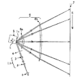
図1は本発明の参考例1の主走査方向の要部断面図(主走査断面図)である。 FIG. 1 is a sectional view (main scanning sectional view) of the main part in the main scanning direction of Reference Example 1 of the present invention.
ここで、主走査方向とは回転多面鏡の回転軸及び結像光学系の光軸に垂直な方向(回転多面鏡で光束が反射偏向(偏向走査)される方向)である。副走査方向とは回転多面鏡の回転軸と平行な方向である。また主走査断面とは主走査方向と結像光学系の光軸を含む平面である。また副走査断面とは主走査断面と垂直な断面である。 Here, the main scanning direction is a direction perpendicular to the rotation axis of the rotating polygon mirror and the optical axis of the imaging optical system (the direction in which the light beam is reflected and deflected (deflected and scanned) by the rotating polygon mirror). The sub-scanning direction is a direction parallel to the rotation axis of the rotary polygon mirror. The main scanning section is a plane including the main scanning direction and the optical axis of the imaging optical system. The sub-scanning section is a section perpendicular to the main scanning section.
同図において1は光源手段であり、例えば波長450nm以下(本参考例では405nm)の光束を発振する窒化ガリウム系の青紫色の半導体レーザー(短波長レーザー)より成っている。本参考例では光源手段1に内蔵する光量検出手段(フォトディテクタ)で得られた信号に基づいて放射する光量を制御手段(不図示)により制御している。2は変換光学素子としてのコリメータレンズであり、光源手段1から発せられた光束を平行光束(もしくは収束光束、もしくは発散光束)に変換している。 In the figure, reference numeral 1 denotes light source means, which is composed of, for example , a gallium nitride blue-violet semiconductor laser (short wavelength laser) that oscillates a light beam having a wavelength of 450 nm or less (405 nm in the present reference example ). In this reference example , the amount of light emitted is controlled by a control means (not shown) based on a signal obtained by a light quantity detection means (photodetector) built in the light source means 1. A collimator lens 2 as a conversion optical element converts a light beam emitted from the light source means 1 into a parallel light beam (or a convergent light beam or a divergent light beam).
3はシリンドリカルレンズであり、副走査断面内にのみ所定のパワーを有しており、コリメータレンズ2により平行光束化した光束を副走査断面内で後述する光偏向器5の偏向面(反射面)5aに主走査方向に長い線像として結像させている。
A cylindrical lens 3 has a predetermined power only in the sub-scan section, and a deflecting surface (reflecting surface) of an
コリメータレンズ2及びシリンドリカルレンズ3等の光学素子は第1の光学系としての入射光学系LAの一要素を構成しており、共に光学ガラスより成るレンズより成っている。 Optical elements such as the collimator lens 2 and the cylindrical lens 3 constitute an element of the incident optical system LA as the first optical system, and both are made of a lens made of optical glass.
尚、コリメータレンズ2とシリンドリカルレンズ3とを1つの光学素子より構成しても良い。 Note that the collimator lens 2 and the cylindrical lens 3 may be constituted by one optical element.
また本参考例においては入射光学系LAを構成する一要素としてシリンドリカルレンズ3を用いているが、これに限らず、例えば反射光学素子としてのシリンドリカルミラーを用いて構成してもよい。さらに入射光学系LAを反射光学素子のみで構成しても良い。 In the present reference example , the cylindrical lens 3 is used as one element constituting the incident optical system LA. However, the present invention is not limited to this. For example, a cylindrical mirror as a reflective optical element may be used. Further, the incident optical system LA may be composed of only a reflective optical element.
4は開口絞りであり、通過光束を制限してビーム形状を整形している。 Reference numeral 4 denotes an aperture stop which shapes the beam shape by limiting the passing light flux.
5は偏向手段としての光偏向器であり、例えば4面構成の回転多面鏡(ポリゴンミラー)より成っており、モータ等の駆動手段(不図示)により一定速度で回転している。
An
6は集光機能とfθ特性とを有する第2の光学系としての結像光学系(fθレンズ系)であり、第1、第2の光学素子(結像レンズ)6a、6bを有し、光偏向器5によって反射偏向された画像情報に基づく光束を被走査面としての感光ドラム面7上に結像させ、かつ副走査断面内において光偏向器5の偏向面と感光ドラム面7との間を共役関係にすることにより、倒れ補償を行っている。
本参考例における第1、第2の光学素子6a、6bは共に日本ゼオン社製Zeonex 330Rから成るプラスチック材料で形成されたトーリックレンズより成っている。尚、プラスチック材料はポリオレフィン系樹脂の一種であり、低吸湿、低GI、低複屈折等の特徴を有している。
The first and second
また第2の光学素子6bは、その入射面(シリンダ面)に環境変動による副走査方向のピントシフト(ピント変動)を補償するための回折光学素子が形成された複合光学素子より成っている。
The second
7は被走査面としての感光ドラム面である。 Reference numeral 7 denotes a photosensitive drum surface as a surface to be scanned.
本参考例において画像情報に応じて光源手段1から光変調され出射した発散光束はコリメータレンズ2により平行光束に変換され、シリンドリカルレンズ3に入射する。シリンドリカルレンズ3に入射した光束のうち主走査断面内においてはそのままの状態で出射して開口絞り4を通過する(一部遮光される)。また副走査断面内においては収束して開口絞り4を通過し(一部遮光される)光偏向器5の偏向面5aにほぼ線像(主走査方向に長手の線像)として結像する。そして光偏向器5の偏向面5aで反射偏向された光束は第1、第2の結像レンズ6a、6bを介して感光ドラム面7上にスポット状に結像され、該光偏向器5を矢印A方向に回転させることによって、該感光ドラム面7上を矢印B方向(主走査方向)に等速度で光走査している。これにより記録媒体としての感光ドラム面7上に画像記録を行なっている。
In this reference example , the divergent light beam that is light-modulated and emitted from the light source means 1 according to the image information is converted into a parallel light beam by the collimator lens 2 and is incident on the cylindrical lens 3. Out of the light beam incident on the cylindrical lens 3, it exits as it is in the main scanning section and passes through the aperture stop 4 (partially shielded). In the sub-scan section, the light beam converges and passes through the aperture stop 4 (partially shielded) to form an almost linear image (a linear image longitudinal in the main scanning direction) on the
図6は日本ゼオン社製ZEONEX 330Rにて成形した3mm厚の平板に対して405nmのレーザ光源を用いてレーザ照射による透過率低下を観測した結果のグラフである。実験の条件はレーザ波長405nm、レーザーパワー20mW、照射密度400mW/cm2、測定環境 25℃及び80℃である。 FIG. 6 is a graph showing a result of observing a decrease in transmittance due to laser irradiation using a 405 nm laser light source on a 3 mm thick flat plate formed by ZEONEX 330R manufactured by ZEON Corporation. The experimental conditions were a laser wavelength of 405 nm, a laser power of 20 mW, an irradiation density of 400 mW / cm 2 , and a measurement environment of 25 ° C. and 80 ° C.
図6から分かるようにレーザ照射により経時的に透過率が低減し、更に高温環境下ではその低下率が非常に大きいことがわかる。このように短波長レーザーを用いた系にプラスチック材より成る光学素子(プラスチック光学素子)を使用しようと考えた場合には、この透過率劣化は無視できない。 As can be seen from FIG. 6, the transmittance decreases with time due to laser irradiation, and the decrease rate is very large under a high temperature environment. Thus, when it is considered to use an optical element (plastic optical element) made of a plastic material in a system using a short wavelength laser, this transmittance deterioration cannot be ignored.
しかしながら、結像光学系(第2の光学系)6においては光偏向器5により常に光束を結像レンズ上6a,6bを走査しているためその単位面積当たりのレーザ露光量は常に同一個所を光束が通過する入射光学系(第1の光学系)LAの光学素子(レンズ)に比べて数十分の1程度となるため、結像光学系6であればプラスチック材より成る光学素子の使用が可能である。
However, in the imaging optical system (second optical system) 6, since the
本参考例においては入射光学系LAを構成する全ての光学素子(コリメータレンズ2及びシリンドリカルレンズ3)の材料を光学ガラスとしたことにより、製品寿命中における透過率変化は微小量となり光源手段(半導体レーザ)1のパッケージ内のフォトディテクタを用いた光量制御だけで被走査面7上を走査する走査光束の光量を所望の光量とすることができる。 In this reference example , the optical glass is used as the material for all the optical elements (collimator lens 2 and cylindrical lens 3) constituting the incident optical system LA, so that the transmittance change during the product lifetime becomes a minute amount and the light source means (semiconductor Laser) The light quantity of the scanning light beam that scans the surface to be scanned 7 can be set to a desired light quantity only by light quantity control using the photodetector in the package.
尚、本参考例においては結像光学系6をプラスチック材より成る光学素子で構成しているが、プラスチック材より成る光学素子に限定されるものではなく、例えば少なくとも一部を光学ガラスより成るレンズで構成しても良い。
In this reference example , the imaging
また本参考例においては結像光学系6を2枚のレンズより構成したが、これに限らず、例えば単一、もしくは3枚以上のレンズより構成しても良い。また回折光学素子を含ませて構成しても良い。
In the present reference example , the imaging
本参考例では、光源手段(半導体レーザ)1の発光部は1個でも複数個でも良い。
[参考例2]
In this reference example , the light source means (semiconductor laser) 1 may have one or more light emitting portions.
[Reference Example 2]
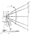
図2は本発明の参考例2の主走査方向の要部断面図(主走査断面図)である。同図において図1に示した要素と同一要素には同符番を付している。 FIG. 2 is a sectional view (main scanning sectional view) of the main part in the main scanning direction of Reference Example 2 of the present invention. In the figure, the same elements as those shown in FIG.
本参考例において前述の参考例1と異なる点は、光源手段1から発した光束の光量を検出する光量検出手段10と、該光量検出手段10の検出結果に基づき該光源手段1の光量を調整する光量補償手段(光量制御手段)11を具備し、かつ入射光学系LAを構成する光学素子のうち、少なくとも1つの光学素子をプラスチック材より成る光学素子より構成したことである。その他の構成及び光学的作用は参考例1と略同様であり、これにより同様な効果を得ている。 This reference example is different from the above-described reference example 1 in that the light quantity detection means 10 detects the light quantity of the light beam emitted from the light source means 1 and the light quantity of the light source means 1 is adjusted based on the detection result of the light quantity detection means 10. The light quantity compensation means (light quantity control means) 11 is provided, and at least one of the optical elements constituting the incident optical system LA is constituted by an optical element made of a plastic material. Other configurations and optical actions are substantially the same as those in Reference Example 1, thereby obtaining the same effects.
即ち、同図において8は温度補償素子であり、プラスチックモールド成型により成形されており、結像光学系6の主走査方向の温度補償(ピント補償)を行っている。
That is, in the figure, reference numeral 8 denotes a temperature compensation element, which is formed by plastic molding, and performs temperature compensation (focus compensation) in the main scanning direction of the imaging
本参考例における温度補償素子8は入射面が主走査断面内に負のパワー(屈折力)を有するシリンダ面(シリンドリカル面)より構成されており、出射面が平面上に主走査断面内に正のパワーを有する回折格子が形成された回折面より構成されている。尚、本参考例において使用しているプラスチック材料(ポリオレフィン系樹脂)は日本ゼオン社製ZEONEX330Rであり、ポリオレフィン系樹脂から成っている。 The temperature compensation element 8 in this reference example is configured by a cylinder surface (cylindrical surface) having an incident surface having negative power (refractive power) in the main scanning section, and the exit surface is positive on the plane in the main scanning section. And a diffraction surface on which a diffraction grating having the following power is formed. The plastic material (polyolefin resin) used in this reference example is ZEONEX330R manufactured by Nippon Zeon Co., Ltd., which is made of polyolefin resin.
9は光路分離手段であり、例えばビームスプリッターより成り、温度補償素子8を通過した後の光束を光偏向器5側と後述する光量検出手段10側への2つに分離している。10は光量検出手段であり、例えばフォトディテクター(受光センサー)等より成り、温度補償素子8より光偏向器5側に配設されており、光路分離手段9で分離された光束の光量を検出している。11は光量補償手段(光量制御手段)であり、光量検出手段10で検出された検出情報(光量)に基づいて光源手段1から発する光束の光量をレーザドライバー12を介して制御(補償)している。
本参考例においては前述した如く入射光学系LAにプラスチック材より成る光学素子を導入した場合には、該プラスチック材より成る光学素子の耐久劣化による透過率低下が無視できないため透過率低下を考慮して光量を制御する必要が生じてくる。 In this reference example , when an optical element made of a plastic material is introduced into the incident optical system LA as described above, a decrease in the transmittance due to durability deterioration of the optical element made of the plastic material cannot be ignored. Therefore, it becomes necessary to control the amount of light.
そこで本参考例においては温度補償素子8を通過した後の光束を光路分離手段9により2つに分離し、該分離した後の一方の光路に光量検出手段10を設け、該光量検出手段10により光量を検出し、該検出した光量データに基づいて光量補償手段11によりレーザドライバー12を介して光源手段1から発する光束の光量制御を行っている。
Therefore, in this reference example , the light flux after passing through the temperature compensation element 8 is separated into two by the optical path separating means 9, and the light
このような構成をとることにより温度補償素子8が耐久劣化し、透過率が変動しても被走査面7上での光量を常に一定に保つことができる。 By adopting such a configuration, the temperature compensation element 8 is deteriorated in durability, and the amount of light on the scanned surface 7 can always be kept constant even if the transmittance varies.
尚、本参考例においては光路分離手段としてビームスプリッターを用いたが、これに限らず、光路が2つに分離できるなら、例えばガラス平板等を用いてもよい。 In this reference example , the beam splitter is used as the optical path separating means. However, the present invention is not limited to this. For example, a glass flat plate may be used as long as the optical path can be separated into two.
また本参考例においてはプラスチック材料としてポリオレフィン系の樹脂材料を用いているが、これに限らず、例えばアクリルやポリカーボネイト等の樹脂材料でも前述の参考例2と同様の効果を発揮することができる。
[参考例3]
In this reference example , a polyolefin-based resin material is used as the plastic material. However, the present invention is not limited to this, and the same effects as those of the above-described reference example 2 can be exhibited even with a resin material such as acrylic or polycarbonate.
[Reference Example 3]
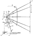
図3は本発明の参考例3の主走査方向の要部断面図(主走査断面図)である。同図において図2に示した要素と同一要素には同符番を付している。 FIG. 3 is a sectional view (main scanning sectional view) of the main part in the main scanning direction of Reference Example 3 of the present invention. In the figure, the same elements as those shown in FIG.
本参考例において前述の参考例2と異なる点は、入射光学系LAを構成するコリメータレンズ21とシリンドリカルレンズ31を共にプラスチック材(ポリオレフィン系樹脂)より成る光学素子より構成したことである。その他の構成及び光学的作用は参考例1と略同様であり、これにより同様な効果を得ている。
This reference example is different from the above-described reference example 2 in that both the
即ち、同図において21はコリメータレンズであり、プラスチックモールド成型より成形している。本参考例ではプラスチックモールド成型の利点を生かし、コリメータレンズ21の少なくとも一方の面に非球面を導入している。これにより本参考例では有効に球面収差を低減している。
That is, in the figure,
31はシリンドリカルレンズであり、プラスチック材で形成されており、その自己温度補償のために入射面が副走査断面内に正のパワー(屈折力)を有するシリンダ面(シリンドリカル面)より成り、出射面が昇温によるピントシフトを補償する回折面より成っている。
本参考例においては前述の参考例2と同様にシリンドリカルレンズ31を通過した後の光束を光路分離手段9により2つに分離し、該分離した後の一方の光路に設けた光量検出手段10により光量を検出し、該検出した光量データに基づいて光量補償手段11によりレーザドライバー12を介して光源手段1から発する光束の光量制御を行っている。これにより被走査面7上での光量変動を効果的に低減でき、且つプラスチックレンズ化による製造の簡易化(コスト低減)が可能となる。
In the present reference example , the light beam after passing through the
尚、本参考例ではコリメータレンズ21とシリンドリカルレンズ31を共にプラスチック材より成る光学素子より構成したが、どちらか一方のみでも良い。
[参考例4]
In this reference example , both the
[Reference Example 4]
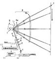
図4は本発明の参考例4の主走査方向の要部断面図(主走査断面図)である。同図において図2に示した要素と同一要素には同符番を付している。 FIG. 4 is a sectional view (main scanning sectional view) of the main part in the main scanning direction of Reference Example 4 of the present invention. In the figure, the same elements as those shown in FIG.
本参考例において前述の参考例2、3と異なる点は、被走査面7と等価な位置(被走査面位置もしくはその近傍)に光量検出手段10を配設したことである。その他の構成及び光学的作用は参考例2、3と略同様であり、これにより同様な効果を得ている。 The present reference example is different from the reference examples 2 and 3 described above in that the light amount detection means 10 is disposed at a position equivalent to the scanned surface 7 (the scanned surface position or its vicinity). Other configurations and optical actions are substantially the same as those in Reference Examples 2 and 3, and the same effects are obtained.
即ち、同図において10は光量検出手段であり、被走査面7と等価な位置(被走査面位置もしくはその近傍)に配設(配置)されており、被走査面7上を走査する走査光束の光量を検出している。
That is, in the figure,
本参考例では被走査面7と等価な位置に配設された光量検出手段10により走査光束の光量を検出し、検出した光量データに基づいて光量補償手段11によりレーザドライバー12を介して光源手段1から発する光束の光量制御を行っている。
In this reference example , the light amount detecting means 10 disposed at a position equivalent to the scanned surface 7 detects the light amount of the scanning light beam, and the light amount compensating means 11 based on the detected light amount data via the
このような構成とすることで、全系を含めた光量制御が可能となり、被走査面7上での光量変動をより効果的に低減することが可能となる。
[実施例1]
With such a configuration, it is possible to control the amount of light including the entire system, and it is possible to more effectively reduce variations in the amount of light on the scanned surface 7.
[Example 1]
図5は本発明の実施例1の主走査方向の要部断面図(主走査断面図)である。同図におい
て図2に示した要素と同一要素には同符番を付している。
FIG. 5 is a sectional view (main scanning sectional view) of the main part in the main scanning direction according to the first embodiment of the present invention. In the figure, the same elements as those shown in FIG.
本実施例において前述の参考例2、3、4と異なる点は、光源手段1の積算発光時間や、本装置を画像形成装置に用いたときの積算プリント枚数等の情報を基に現在のプラスチック材より成る光学素子の透過率を予測し、その予測に基づいて光量制御を行うようにしたことである。その他の構成及び光学的作用は参考例2、3、4と略同様であり、これにより同様な効果を得ている。 This embodiment differs from the above-mentioned Reference Examples 2, 3, and 4 in that the current plastic is based on information such as the accumulated light emission time of the light source means 1 and the accumulated number of printed sheets when this apparatus is used in an image forming apparatus. That is, the transmittance of the optical element made of the material is predicted, and the light amount control is performed based on the prediction. Other configurations and optical actions are substantially the same as those of Reference Examples 2, 3, and 4, thereby obtaining the same effects.
即ち、本実施例では入射光学系LAの一部を構成するプラスチック材より成る光学素子の耐久劣化に伴う透過率変化(透過率低下データ)を予測し、その予測を元に光量補償量を決定する光量補償量決定手段13と、該光量補償量決定手段13からの光量補償量に基づき該光源手段1から発する光束の光量を調整する光量補償手段11と、を具備し、該光量補償手段11によりレーザドライバー12を介して光源手段1から発する光束の光量制御を行っている。
That is, in this embodiment, a change in transmittance (transmittance reduction data) due to durability deterioration of an optical element made of a plastic material constituting a part of the incident optical system LA is predicted, and a light amount compensation amount is determined based on the prediction. A light amount compensation amount determining means 13 for adjusting the light amount of the light beam emitted from the light source means 1 based on the light amount compensation amount from the light amount compensation
本実施例における光量補償量決定手段13は、光源手段1の積算発光時間をもとにプラスチック材より成る光学素子の耐久劣化に伴う透過率変化を予測(作成)している。 The light amount compensation amount determining means 13 in this embodiment predicts (creates) a change in transmittance accompanying durability deterioration of an optical element made of a plastic material based on the accumulated light emission time of the light source means 1.
又は/及び画像形成装置に用いたときのプリント枚数を元にプラスチック材より成る光学素子の耐久劣化に伴う透過率変化を予測している。 Or / and a change in transmittance due to deterioration of durability of an optical element made of a plastic material is predicted based on the number of printed sheets when used in an image forming apparatus.
このように本実施例では前記図6に示すようなプラスチック材より成る光学素子の透過率変化情報を光量補償量決定手段13に持たせることにより、光源手段1の積算発光時間や画像形成装置の積算プリント枚数等の情報から光量補償値を決定し補償を行うことにより、複雑な光量検出機構を必要とせずに被走査面7上での光量を常に一定に保つことを可能としている。
As described above, in this embodiment, the light amount compensation
[画像形成装置]
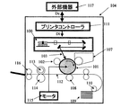
図8は本発明の画像形成装置の実施例を示す副走査方向の要部断面図である。図において、符号104は画像形成装置を示す。この画像形成装置104には、パーソナルコンピュータ等の外部機器117からコードデータDcが入力する。このコードデータDcは、装置内のプリンタコントローラ111によって、画像データ(ドットデータ)Diに変換される。この画像データDiは、参考例1〜4、実施例1のいずれかに示した構成を有する光走査ユニット100に入力される。そして、この光走査ユニット100からは、画像データDiに応じて変調された光ビーム103が出射され、この光ビーム103によって感光ドラム101の感光面が主走査方向に走査される。
[Image forming apparatus]
FIG. 8 is a cross-sectional view of the main part in the sub-scanning direction showing an embodiment of the image forming apparatus of the present invention. In the figure,
静電潜像担持体(感光体)たる感光ドラム101は、モータ115によって時計廻りに回転させられる。そして、この回転に伴って、感光ドラム101の感光面が光ビーム103に対して、主走査方向と直交する副走査方向に移動する。感光ドラム101の上方には、感光ドラム101の表面を一様に帯電せしめる帯電ローラ102が表面に当接するように設けられている。そして、帯電ローラ102によって帯電された感光ドラム101の表面に、前記光走査ユニット100によって走査される光ビーム103が照射されるようになっている。
The
先に説明したように、光ビーム103は、画像データDiに基づいて変調されており、この光ビーム103を照射することによって感光ドラム101の表面に静電潜像を形成せしめる。この静電潜像は、上記光ビーム103の照射位置よりもさらに感光ドラム101の回転方向の下流側で感光ドラム101に当接するように配設された現像器107によってトナー像として現像される。
As described above, the
現像器107によって現像されたトナー像は、感光ドラム101の下方で、感光ドラム101に対向するように配設された転写ローラ(転写器)108によって被転写材たる用紙112上に転写される。用紙112は感光ドラム101の前方(図8において右側)の用紙カセット109内に収納されているが、手差しでも給紙が可能である。用紙カセット109端部には、給紙ローラ110が配設されており、用紙カセット109内の用紙112を搬送路へ送り込む。
The toner image developed by the developing
以上のようにして、未定着トナー像を転写された用紙112はさらに感光ドラム101後方(図8おいて左側)の定着器へと搬送される。定着器は内部に定着ヒータ(図示せず)を有する定着ローラ113とこの定着ローラ113に圧接するように配設された加圧ローラ114とで構成されており、転写部から搬送されてきた用紙112を定着ローラ113と加圧ローラ114の圧接部にて加圧しながら加熱することにより用紙112上の未定着トナー像を定着せしめる。更に定着ローラ113の後方には排紙ローラ116が配設されており、定着された用紙112を画像形成装置の外に排出せしめる。
As described above, the
図8においては図示していないが、プリントコントローラ111は、先に説明したデータの変換だけでなく、モータ115を始め画像形成装置内の各部や、後述する光走査ユニット内のポリゴンモータなどの制御を行う。
Although not shown in FIG. 8, the
本発明で使用される画像形成装置の記録密度は、特に限定されない。しかし、記録密度が高くなればなるほど、高画質が求められることを考えると、1200dpi以上の画像形成装置において本発明の参考例1〜4、実施例1の構成はより効果を発揮する。 The recording density of the image forming apparatus used in the present invention is not particularly limited. However, considering that the higher the recording density, the higher the image quality is required, the configurations of Reference Examples 1 to 4 and Example 1 of the present invention are more effective in an image forming apparatus of 1200 dpi or more.
[カラー画像形成装置]
図9は本発明の実施例のカラー画像形成装置の要部概略図である。本実施例は、光走査装置を4個並べ各々並行して像担持体である感光ドラム面上に画像情報を記録するタンデムタイプのカラー画像形成装置である。図9において、60はカラー画像形成装置、61,62,63,64は各々参考例1〜4、実施例1に示したいずれかの構成を有する光走査装置、21,22,23,24は各々像担持体としての感光ドラム、31,32,33,34は各々現像器、51は搬送ベルトである。
[Color image forming apparatus]
FIG. 9 is a schematic view of a main part of a color image forming apparatus according to an embodiment of the present invention. This embodiment is a tandem type color image forming apparatus in which four optical scanning devices are arranged in parallel and image information is recorded on a photosensitive drum surface as an image carrier. In FIG. 9, 60 is a color image forming apparatus, 61, 62, 63, and 64 are reference examples 1 to 4, respectively, and
図9において、カラー画像形成装置60には、パーソナルコンピュータ等の外部機器52からR(レッド)、G(グリーン)、B(ブルー)の各色信号が入力する。これらの色信号は、装置内のプリンタコントローラ53によって、C(シアン),M(マゼンタ),Y(イエロー)、B(ブラック)の各画像データ(ドットデータ)に変換される。これらの画像データは、それぞれ光走査装置61,62,63,64に入力される。そして、これらの光走査装置からは、各画像データに応じて変調された光ビーム41,42,43,44が出射され、これらの光ビームによって感光ドラム21,22,23,24の感光面が主走査方向に走査される。
In FIG. 9, the color
本実施例におけるカラー画像形成装置は光走査装置(61,62,63,64)を4個並べ、各々がC(シアン),M(マゼンタ),Y(イエロー)、B(ブラック)の各色に対応し、各々平行して感光ドラム21,22,23,24面上に画像信号(画像情報)を記録し、カラー画像を高速に印字するものである。
The color image forming apparatus in this embodiment has four optical scanning devices (61, 62, 63, 64) arranged in each color of C (cyan), M (magenta), Y (yellow), and B (black). Correspondingly, image signals (image information) are recorded on the
本実施例におけるカラー画像形成装置は上述の如く4つの光走査装置61,62,63,64により各々の画像データに基づいた光ビームを用いて各色の潜像を各々対応する感光ドラム21,22,23,24面上に形成している。その後、記録材に多重転写して1枚のフルカラー画像を形成している。
As described above, the color image forming apparatus in this embodiment uses the light beams based on the respective image data by the four
前記外部機器52としては、例えばCCDセンサを備えたカラー画像読取装置が用いられても良い。この場合には、このカラー画像読取装置と、カラー画像形成装置60とで、カラーデジタル複写機が構成される。
As the
1 光源手段(短波長レーザー)
2、21 変換光学素子(コリメータレンズ)
3、31 レンズ系(シリンドリカルレンズ)
4 開口絞り
5 偏向手段(ポリゴンミラー)
6 第2の光学系(結像光学系)
6a,6b 結像レンズ
7 被走査面(感光体ドラム)
LA 第1の光学系(入射光学系)
9 光路分離手段
10 光量検出手段
11 光量補償手段
12 レーザドライバー
13 光量補償量決定手段
61、62、63、64 光走査装置
21、22、23、24 像担持体(感光ドラム)
31、32、33、34 現像器
41、42、43、44 光束
51 搬送ベルト
52 外部機器
53 プリンタコントローラ
60 カラー画像形成装置
100 光走査装置
101 感光ドラム
102 帯電ローラ
103 光ビーム
104 画像形成装置
107 現像装置
108 転写ローラ
109 用紙カセット
110 給紙ローラ
111 プリンタコントローラ
112 転写材(用紙)
113 定着ローラ
114 加圧ローラ
115 モータ
116 排紙ローラ
117 外部機器
1 Light source means (short wavelength laser)
2, 21 Conversion optical element (collimator lens)
3, 31 Lens system (cylindrical lens)
4
6 Second optical system (imaging optical system)
6a, 6b Imaging lens 7 Scanned surface (photosensitive drum)
LA first optical system (incident optical system)
DESCRIPTION OF
31, 32, 33, 34
113
Claims (4)
前記第1の光学系を構成する光学素子のうち少なくとも1つの光学素子は、ポリオレフィン系樹脂より成り、前記光源手段の積算発光時間を元に作成された前記ポリオレフィン系樹脂より成る光学素子の耐久劣化に伴う透過率低下データを元に光量補償量を決定する光量補償量決定手段と、前記光量補償量決定手段からの光量補償量に基づき前記光源手段の発光部から出射される光束の光量を調整する光量補償手段と、を有することを特徴とする光走査装置。 Light source means including a light emitting unit that emits a light beam having a wavelength of 450 nm or less, a first optical system that guides the light beam emitted from the light emitting unit of the light source means to the deflecting unit, and deflection by the deflection surface of the deflecting unit A second optical system that forms an image on the surface to be scanned.
At least one optical element among the optical elements constituting the first optical system is made of a polyolefin-based resin, and durability deterioration of the optical element made of the polyolefin-based resin prepared based on the accumulated light emission time of the light source means A light amount compensation amount determining means for determining a light amount compensation amount based on the transmittance reduction data associated with the light amount, and adjusting the light amount of the light beam emitted from the light emitting unit of the light source means based on the light amount compensation amount from the light amount compensation amount determining means And a light quantity compensation means for performing the above.
Priority Applications (1)
| Application Number | Priority Date | Filing Date | Title |
|---|---|---|---|
| JP2005136283A JP4677277B2 (en) | 2005-05-09 | 2005-05-09 | Optical scanning device and image forming apparatus using the same |
Applications Claiming Priority (1)
| Application Number | Priority Date | Filing Date | Title |
|---|---|---|---|
| JP2005136283A JP4677277B2 (en) | 2005-05-09 | 2005-05-09 | Optical scanning device and image forming apparatus using the same |
Publications (3)
| Publication Number | Publication Date |
|---|---|
| JP2006313268A JP2006313268A (en) | 2006-11-16 |
| JP2006313268A5 JP2006313268A5 (en) | 2008-06-19 |
| JP4677277B2 true JP4677277B2 (en) | 2011-04-27 |
Family
ID=37534784
Family Applications (1)
| Application Number | Title | Priority Date | Filing Date |
|---|---|---|---|
| JP2005136283A Expired - Fee Related JP4677277B2 (en) | 2005-05-09 | 2005-05-09 | Optical scanning device and image forming apparatus using the same |
Country Status (1)
| Country | Link |
|---|---|
| JP (1) | JP4677277B2 (en) |
Families Citing this family (6)
| Publication number | Priority date | Publication date | Assignee | Title |
|---|---|---|---|---|
| JP5012349B2 (en) | 2007-09-14 | 2012-08-29 | ブラザー工業株式会社 | Optical scanning apparatus and image forming apparatus |
| US8027074B2 (en) | 2007-12-07 | 2011-09-27 | Konica Minolta Opto, Inc. | Scan optical system, light scan device, and image formation device |
| JP5246170B2 (en) | 2008-01-31 | 2013-07-24 | コニカミノルタアドバンストレイヤー株式会社 | Scanning optical system, optical scanning device, and image forming apparatus |
| JP2009294305A (en) * | 2008-06-03 | 2009-12-17 | Ricoh Co Ltd | Optical scanner, multi-beam scanner and image forming apparatus |
| JP2010061110A (en) * | 2008-08-07 | 2010-03-18 | Kyocera Mita Corp | Light scanning optical device, image forming device using same, and light scanning method |
| JP2010039326A (en) * | 2008-08-07 | 2010-02-18 | Kyocera Mita Corp | Optical scanning optical apparatus, image forming apparatus using the same and method of correcting change in position of focal point in sub-scanning direction due to temperature change |
Family Cites Families (8)
| Publication number | Priority date | Publication date | Assignee | Title |
|---|---|---|---|---|
| JP2002113899A (en) * | 2000-10-05 | 2002-04-16 | Fuji Xerox Co Ltd | Imaging apparatus |
| JP3507474B2 (en) * | 2001-01-11 | 2004-03-15 | キヤノン株式会社 | Optical scanning device and image forming apparatus using the same |
| JP3478819B1 (en) * | 2001-01-11 | 2003-12-15 | キヤノン株式会社 | Optical scanning device and image forming apparatus using the same |
| JP2004145352A (en) * | 2001-01-11 | 2004-05-20 | Canon Inc | Optical scanner and image forming apparatus using the same |
| JP2003215485A (en) * | 2002-01-24 | 2003-07-30 | Fuji Xerox Co Ltd | Optical scanner |
| JP2003211728A (en) * | 2002-01-25 | 2003-07-29 | Fuji Xerox Co Ltd | Imaging apparatus |
| JP2004045840A (en) * | 2002-07-12 | 2004-02-12 | Ricoh Co Ltd | Method and device for optical scanning, and image forming device |
| JP2005070124A (en) * | 2003-08-27 | 2005-03-17 | Canon Inc | Optical scanner and image forming apparatus using same |
-
2005
- 2005-05-09 JP JP2005136283A patent/JP4677277B2/en not_active Expired - Fee Related
Also Published As
| Publication number | Publication date |
|---|---|
| JP2006313268A (en) | 2006-11-16 |
Similar Documents
| Publication | Publication Date | Title |
|---|---|---|
| JP4314010B2 (en) | Optical scanning device and image forming apparatus using the same | |
| US8654168B2 (en) | Optical scanning device, image forming apparatus, and optical scanning device designing method | |
| JP4641478B2 (en) | Optical scanning device and image forming apparatus using the same | |
| JP4750259B2 (en) | Optical scanning device and image forming apparatus using the same | |
| JP4378082B2 (en) | Scanning optical device and image forming apparatus using the same | |
| JP4590166B2 (en) | Optical scanning device and image forming apparatus using the same | |
| JP4677277B2 (en) | Optical scanning device and image forming apparatus using the same | |
| JP4819436B2 (en) | Optical scanning device and method of adjusting optical scanning device | |
| JP2007114484A (en) | Optical scanner and image forming device using it | |
| JP2008224943A (en) | Optical scanner and image forming apparatus using the same | |
| JP4444605B2 (en) | Optical scanning device and image forming apparatus using the same | |
| JP4769733B2 (en) | Optical scanning device and image forming apparatus using the same | |
| JP4455309B2 (en) | Optical scanning device and image forming apparatus using the same | |
| JP4411054B2 (en) | Optical scanning device and image forming apparatus using the same | |
| JP2007045094A (en) | Scanning optical system and image forming device using the same | |
| JP4401950B2 (en) | Optical scanning device and image forming apparatus using the same | |
| JP4401951B2 (en) | Optical scanning device and image forming apparatus using the same | |
| JP2005088352A (en) | Scanning optical device and image forming apparatus using it | |
| JP2005070125A (en) | Optical scanner and image forming apparatus using same | |
| JP4630593B2 (en) | Scanning optical device and image forming apparatus using the same | |
| JP2010061110A (en) | Light scanning optical device, image forming device using same, and light scanning method | |
| JP2011154118A (en) | Light scanning optical device, and image forming apparatus using the same | |
| JP2004317790A (en) | Optical scanner | |
| JP5100197B2 (en) | Adjusting method and manufacturing method of optical scanning device | |
| JP4418775B2 (en) | Multi-beam scanning device and image forming apparatus using the same |
Legal Events
| Date | Code | Title | Description |
|---|---|---|---|
| A521 | Request for written amendment filed |
Free format text: JAPANESE INTERMEDIATE CODE: A523 Effective date: 20080507 |
|
| A621 | Written request for application examination |
Free format text: JAPANESE INTERMEDIATE CODE: A621 Effective date: 20080507 |
|
| A977 | Report on retrieval |
Free format text: JAPANESE INTERMEDIATE CODE: A971007 Effective date: 20101027 |
|
| A131 | Notification of reasons for refusal |
Free format text: JAPANESE INTERMEDIATE CODE: A131 Effective date: 20101102 |
|
| A521 | Request for written amendment filed |
Free format text: JAPANESE INTERMEDIATE CODE: A523 Effective date: 20101224 |
|
| TRDD | Decision of grant or rejection written | ||
| A01 | Written decision to grant a patent or to grant a registration (utility model) |
Free format text: JAPANESE INTERMEDIATE CODE: A01 Effective date: 20110125 |
|
| A01 | Written decision to grant a patent or to grant a registration (utility model) |
Free format text: JAPANESE INTERMEDIATE CODE: A01 |
|
| A61 | First payment of annual fees (during grant procedure) |
Free format text: JAPANESE INTERMEDIATE CODE: A61 Effective date: 20110131 |
|
| FPAY | Renewal fee payment (event date is renewal date of database) |
Free format text: PAYMENT UNTIL: 20140204 Year of fee payment: 3 |
|
| R150 | Certificate of patent or registration of utility model |
Free format text: JAPANESE INTERMEDIATE CODE: R150 |
|
| LAPS | Cancellation because of no payment of annual fees |