JP4674002B2 - POSITION DETECTING DEVICE, POSITION DETECTING METHOD, ELECTRONIC COMPONENT CONVEYING DEVICE, AND ELECTRON BEAM EXPOSURE DEVICE - Google Patents
POSITION DETECTING DEVICE, POSITION DETECTING METHOD, ELECTRONIC COMPONENT CONVEYING DEVICE, AND ELECTRON BEAM EXPOSURE DEVICE Download PDFInfo
- Publication number
- JP4674002B2 JP4674002B2 JP2001161328A JP2001161328A JP4674002B2 JP 4674002 B2 JP4674002 B2 JP 4674002B2 JP 2001161328 A JP2001161328 A JP 2001161328A JP 2001161328 A JP2001161328 A JP 2001161328A JP 4674002 B2 JP4674002 B2 JP 4674002B2
- Authority
- JP
- Japan
- Prior art keywords
- phase
- input image
- image
- frequency
- mark
- Prior art date
- Legal status (The legal status is an assumption and is not a legal conclusion. Google has not performed a legal analysis and makes no representation as to the accuracy of the status listed.)
- Expired - Fee Related
Links
Images


Classifications
-
- G—PHYSICS
- G03—PHOTOGRAPHY; CINEMATOGRAPHY; ANALOGOUS TECHNIQUES USING WAVES OTHER THAN OPTICAL WAVES; ELECTROGRAPHY; HOLOGRAPHY
- G03F—PHOTOMECHANICAL PRODUCTION OF TEXTURED OR PATTERNED SURFACES, e.g. FOR PRINTING, FOR PROCESSING OF SEMICONDUCTOR DEVICES; MATERIALS THEREFOR; ORIGINALS THEREFOR; APPARATUS SPECIALLY ADAPTED THEREFOR
- G03F9/00—Registration or positioning of originals, masks, frames, photographic sheets or textured or patterned surfaces, e.g. automatically
- G03F9/70—Registration or positioning of originals, masks, frames, photographic sheets or textured or patterned surfaces, e.g. automatically for microlithography
- G03F9/7088—Alignment mark detection, e.g. TTR, TTL, off-axis detection, array detector, video detection
-
- G—PHYSICS
- G01—MEASURING; TESTING
- G01B—MEASURING LENGTH, THICKNESS OR SIMILAR LINEAR DIMENSIONS; MEASURING ANGLES; MEASURING AREAS; MEASURING IRREGULARITIES OF SURFACES OR CONTOURS
- G01B11/00—Measuring arrangements characterised by the use of optical techniques
-
- G—PHYSICS
- G03—PHOTOGRAPHY; CINEMATOGRAPHY; ANALOGOUS TECHNIQUES USING WAVES OTHER THAN OPTICAL WAVES; ELECTROGRAPHY; HOLOGRAPHY
- G03F—PHOTOMECHANICAL PRODUCTION OF TEXTURED OR PATTERNED SURFACES, e.g. FOR PRINTING, FOR PROCESSING OF SEMICONDUCTOR DEVICES; MATERIALS THEREFOR; ORIGINALS THEREFOR; APPARATUS SPECIALLY ADAPTED THEREFOR
- G03F9/00—Registration or positioning of originals, masks, frames, photographic sheets or textured or patterned surfaces, e.g. automatically
- G03F9/70—Registration or positioning of originals, masks, frames, photographic sheets or textured or patterned surfaces, e.g. automatically for microlithography
- G03F9/7092—Signal processing
-
- H—ELECTRICITY
- H01—ELECTRIC ELEMENTS
- H01J—ELECTRIC DISCHARGE TUBES OR DISCHARGE LAMPS
- H01J37/00—Discharge tubes with provision for introducing objects or material to be exposed to the discharge, e.g. for the purpose of examination or processing thereof
- H01J37/30—Electron-beam or ion-beam tubes for localised treatment of objects
- H01J37/304—Controlling tubes by information coming from the objects or from the beam, e.g. correction signals
- H01J37/3045—Object or beam position registration
-
- H—ELECTRICITY
- H01—ELECTRIC ELEMENTS
- H01J—ELECTRIC DISCHARGE TUBES OR DISCHARGE LAMPS
- H01J2237/00—Discharge tubes exposing object to beam, e.g. for analysis treatment, etching, imaging
- H01J2237/30—Electron or ion beam tubes for processing objects
- H01J2237/317—Processing objects on a microscale
- H01J2237/3175—Lithography
Description
【0001】
【発明の属する技術分野】
本発明は、テンプレート画像に近似したマークの位置を入力画像から検出する位置検出装置、位置検出装置を有する電子部品搬送装置、位置検出装置を有する電子ビーム露光装置及び位置検出方法に関する。特に本発明は、入力画像の輝度分布の変化やマークの変形の影響を最小限にして精度よく入力画像からマークの位置を検出する位置検出装置、位置検出装置を有する電子部品搬送装置、位置検出装置を有する電子ビーム露光装置及び位置検出方法に関する。
【0002】
【従来の技術】
大規模集積回路(LSI)の製造工程においては、半導体などのウェハ基板に微細な回路パターンを露光する工程や、様々な膜を成膜する工程などを繰り返す必要がある。LSIに設計どおりの機能を持たせるためには、各処理ごとにウェハ基板を正確な位置に合わせなければならない。そこで、予めウェハ基板にマークを設けておき、マークの位置を観察することによりウェハ基板の位置合わせを行っている。従来、テンプレート画像とウェハ基板を撮影した入力画像との輝度分布を比較して入力画像中のマークの位置を検出するパターンマッチング処理が行われている。
【0003】
【発明が解決しようとする課題】
しかし、ウェハ基板上に様々な膜を積層していくと、マークの近傍で輝度値が局所的に変化することがあり、マークの形状が変形して観察されることがある。また、ウェハ基板を化学的機械研磨(CMP)処理する際に、マークのエッジが欠損することもあり、この場合もマークの形状が変形して観測されてしまう。さらに、CMP処理により下地の層の膜厚がウェハ基板内で不均一となり、その上にさらに他の膜を成膜すると、膜厚の違いにより反射光の強度が局所的に変化することがある。このような場合、従来の輝度値を用いるパターンマッチング処理ではウェハ基板を正確に位置合わせできないという問題があった。
【0004】
そこで本発明は、上記の課題を解決することのできる位置検出装置、位置検出装置を有する電子部品搬送装置、位置検出装置を有する電子ビーム露光装置及び位置検出方法を提供することを目的とする。この目的は特許請求の範囲における独立項に記載の特徴の組み合わせにより達成される。また従属項は本発明の更なる有利な具体例を規定する。
【0005】
【課題を解決するための手段】
即ち、本発明の第1の形態によると、テンプレート画像に近似したマークの位置を入力画像から検出する位置検出装置であって、テンプレート画像中の所定の位置を基準としてテンプレート画像を周波数成分に変換した場合の位相成分と、入力画像中の所定の位置を基準として入力画像を周波数成分に変換した場合の位相成分との位相成分差を周波数ごとに算出する位相差算出手段と、位相差算出手段が算出した位相成分差を変換した位相インパルス応答関数に基づいて、入力画像中のマークの位置を検出するマーク位置検出手段とを備えることを特徴とする位置検出装置を提供する。
【0006】
位相差算出手段は、テンプレート画像を基準とした入力画像の周波数応答関数に基づいて、位相成分差を算出するのが好ましい。マーク位置検出手段は、2次元離散フーリエ逆変換により位相インパルス応答関数を算出してよい。2次元離散フーリエ変換は高速フーリエ変換であってよい。
【0007】
マーク位置検出手段は、所定の条件を満たす位相インパルス応答関数値を与える座標を入力画像から検出する座標検出手段を有し、座標検出手段が検出した座標に基づいて、マークの位置を検出してよい。
【0008】
座標検出手段は、位相インパルス応答関数値が最大となる座標を検出してよい。座標検出手段は、インパルス応答関数値の絶対値が最大である座標を検出してもよい。座標検出手段は、位相インパルス応答関数値と所定値との差の絶対値が最大である座標を検出してもよい。座標検出手段は、位相インパルス応答関数値が極値である座標を検出してもよい。座標検出手段は、位相インパルス応答関数値と所定値との差の絶対値が最大である座標を検出してもよい。
【0009】
位置検出装置は、入力画像を周波数成分に変換する変換手段をさらに備えてもよい。変換手段は、2次元離散フーリエ変換により入力画像を周波数成分に変換してよい。2次元離散フーリエ変換は高速フーリエ変換であってよい。
【0010】
位置検出装置は、入力画像から、テンプレート画像と実質的に等しい大きさの比較領域を選択する比較領域選択手段をさらに備えてもよく、変換手段は、比較領域において、テンプレート画像中の基準となる所定の位置に対応する座標を入力画像中の基準となる所定の位置として比較領域を周波数成分に変換してもよい。
【0011】
比較領域選択手段は、各比較領域が所定のパーセントずつ重複するように、入力画像から比較領域を選択してよい。具体的には、位置検出装置は、入力画像を、テンプレート画像より小さい予備領域に分割する入力画像分割手段をさらに備えてもよく、比較領域選択手段は、各予備領域を所定の位置にそれぞれ含むように比較領域を選択してもよい。
【0012】
位置検出装置は、比較領域の端部の画素値が実質的に等しくなるように、比較領域の画素値を補正する補正手段をさらに備えてもよい。補正手段は、テンプレート画像の端部の画素値が実質的に等しくなるように、テンプレート画像の画素値を補正してもよい。比較領域選択手段は、一辺がそれぞれ2のm乗(mは正の整数)の画素数を持つように比較領域を選択してもよい。比較領域選択手段は、比較領域の画素数を調整する手段を有してもよい。
【0013】
マーク位置検出手段は、位相成分差を変換した位相インパルス応答関数に基づいて、所定の条件を満たす位相インパルス応答関数値を与える座標を含む比較領域を検出する比較領域検出手段をさらに有してもよく、入力画像における比較領域の位置と、比較領域中の座標とに基づいて、マークの位置を検出してもよい。
【0014】
マーク位置検出手段は、各比較領域から所定の領域を選択して、所定の領域における位相インパルス応答関数値を抽出する手段と、抽出した位相インパルス応答関数値から所定の条件を満たす位相インパルス応答関数値を選択する手段とをさらに有してもよく、選択した位相インパルス応答関数値を与える座標を検出してよい。
【0015】
マーク位置検出手段は、比較領域の位相成分差を変換した位相インパルス応答関数に基づいて、比較領域における位相インパルス応答関数値を所定の閾値と比較することにより、マークが当該比較領域に含まれるか否かを判断するマーク判断手段をさらに有してもよい。
【0016】
位置検出装置は、所定の帯域以下の周波数成分の位相成分を抽出する低域抽出フィルタをさらに備えてもよく、マーク位置検出手段は、低域抽出フィルタが抽出したテンプレート画像の位相成分と低域抽出フィルタが抽出した入力画像の位相成分との位相成分差を変換した位相インパルス応答関数に基づいて、入力画像中のマークの位置を検出してもよい。
【0017】
位置検出装置は、テンプレート画像を周波数成分に変換した場合の振幅の値に基づいて定めた周波数における位相成分を当該周波数に対応づけて保持するテンプレート画像保持手段をさらに備えてもよく、位相差算出手段は、入力画像を周波数成分に変換した場合の位相成分のうち、テンプレート画像保持手段が保持する周波数に対応する周波数の位相成分と、テンプレート画像保持手段が保持するテンプレート画像の位相成分との位相成分差を周波数ごとに算出してもよい。
【0018】
変換手段は、テンプレート画像を周波数成分に変換してもよい。位置検出装置は、テンプレート画像を周波数成分に変換した場合の位相成分を周波数に対応づけて保持するテンプレート画像保持手段をさらに備えてもよい。テンプレート画像は、一辺がそれぞれ2のn乗(nは正の整数)の画素数を持つのが好ましい。
【0019】
位置検出装置は、テンプレート画像の逆周波数特性を持つテンプレート逆画像を保持するテンプレート画像保持手段と、テンプレート逆画像と入力画像との畳込み積分画像を形成する畳込み積分手段と、畳込み画像を所定の位置を基準として周波数成分に変換する変換手段とをさらに備えてもよく、位相差算出手段は、畳込み画像の周波数成分の位相成分を位相成分差として算出してもよい。
【0020】
本発明の第2の形態によると、テンプレート画像に近似したマークの位置を入力画像から検出する位置検出方法であって、テンプレート画像中の所定の位置を基準としてテンプレート画像を周波数成分に変換した場合の位相成分と、入力画像中の所定の位置を基準として入力画像を周波数成分に変換した場合の位相成分との位相成分差を周波数ごとに算出する位相成分差算出ステップと、位相成分差を位相インパルス応答関数に変換する逆変換ステップを有し、位相インパルス応答関数に基づいて入力画像中のマークの位置を検出するマーク位置検出ステップとを備えることを特徴とする位置検出方法を提供する。
【0021】
マーク位置検出ステップは、位相成分差を位相インパルス応答関数に変換する逆変換ステップを有し、位相インパルス応答関数に基づいて入力画像中のマークの位置を検出してよい。
【0022】
逆変換ステップは、2次元離散フーリエ逆変換により位相インパルス応答関数を算出してよい。マーク位置検出ステップは、所定の条件を満たす位相インパルス応答関数値を与える座標を入力画像から検出する座標検出ステップを有してもよく、検出された座標に基づいて、マークの位置を検出してよい。
【0023】
座標検出ステップは、位相インパルス応答関数値が最大となる座標を検出してもよい。座標検出ステップは、インパルス応答関数値の絶対値が最大である座標を検出してもよい。座標検出ステップは、位相インパルス応答関数値と所定値との差の絶対値が最大である座標を検出してもよい。座標検出ステップは、位相インパルス応答関数値が極値である座標を検出してもよい。座標検出ステップは、位相インパルス応答関数値と所定値との差の絶対値が最大である座標を検出してもよい。
【0024】
位置検出方法は、入力画像を周波数成分に変換する変換ステップをさらに備えてもよい。変換ステップは、2次元離散フーリエ変換により入力画像を周波数成分に変換してもよい。
【0025】
入力画像から、テンプレート画像と実質的に等しい大きさの比較領域を選択する比較領域選択ステップをさらに備えてもよく、変換ステップは、比較領域において、テンプレート画像中の基準となる所定の位置に対応する座標を入力画像中の基準となる所定の位置として比較領域を周波数成分に変換してもよい。
【0026】
入力画像を、テンプレート画像より小さい予備領域に分割する入力画像分割ステップをさらに備えてもよく、比較領域選択ステップは、各予備領域を所定の位置にそれぞれ含むように比較領域を選択してよい。
【0027】
位置検出方法は、比較領域の端部の画素値が実質的に等しくなるように、比較領域の画素値を補正する補正ステップをさらに備えてもよい。比較領域選択ステップは、一辺がそれぞれ2のm乗(mは正の整数)の画素数を持つように比較領域を選択してよい。
【0028】
マーク位置検出ステップは、位相成分差を変換した位相インパルス応答関数に基づいて、所定の条件を満たす位相インパルス応答関数値を与える座標を含む比較領域を検出する比較領域検出ステップをさらに有してもよく、入力画像における比較領域の位置と、比較領域中の座標とに基づいて、マークの位置を検出してよい。
【0029】
マーク位置検出ステップは、比較領域から所定の領域を選択するステップと、所定の領域における位相インパルス応答関数値を抽出する抽出ステップと、抽出した位相インパルス応答関数値から所定の条件を満たす位相インパルス応答関数値を選択するステップとをさらに有してよく、選択した位相インパルス応答関数値を与える座標を検出してよい。
【0030】
マーク位置検出ステップは、比較領域の位相成分差を変換した位相インパルス応答関数に基づいて、比較領域における位相インパルス応答関数値を所定の閾値と比較することにより、マークが当該比較領域に含まれるか否かを判断するマーク判断ステップを有してもよい。
【0031】
位置検出方法は、所定の帯域以下の周波数成分の位相成分を抽出する低域抽出ステップをさらに備えてもよく、マーク位置検出ステップは、低域抽出ステップにおいて抽出されたテンプレート画像の位相成分と、低域抽出ステップにおいて抽出された入力画像の位相成分との位相成分差に基づいて、入力画像中のマークの位置を検出してもよい。
【0032】
位置検出方法は、テンプレート画像を周波数成分に変換した場合の振幅の値に基づいて定めた周波数における位相成分を当該周波数に対応づけて保持するテンプレート周波数保持ステップをさらに備えてもよく、位相成分差算出ステップは、入力画像を周波数成分に変換した場合の位相成分のうち、テンプレート周波数保持ステップにおいて保持された周波数に対応する周波数の位相成分と、テンプレート周波数保持ステップにおいて保持されたテンプレート画像の位相成分との位相成分差を周波数ごとに算出してよい。
【0033】
位置検出方法は、テンプレート画像を2次元離散フーリエ変換により周波数成分に変換する変換ステップをさらに備えてもよい。位置検出方法は、テンプレート画像を周波数成分に変換した場合の位相成分を周波数に対応づけて保持するテンプレート画像保持ステップをさらに備えてもよい。位置検出方法は、テンプレート画像が、一辺がそれぞれ2のn乗(nは正の整数)の画素数を持つようにテンプレート画像を選択するステップをさらに備えてもよい。位置検出方法は、テンプレート画像の端部の画素値が実質的に等しくなるように、テンプレート画像の画素値を補正する補正ステップをさらに備えてもよい。
【0034】
位置検出方法は、テンプレート画像の逆周波数特性を持つテンプレート逆画像を保持するテンプレート画像保持ステップと、テンプレート逆画像と入力画像との畳込み積分画像を形成する畳込み積分画像形成ステップと、畳込み画像を所定の位置を基準として周波数成分に変換する変換ステップとをさらに備えてもよく、位相成分差算出ステップは、畳込み画像中の基準位置からの位相成分を位相成分差として算出してよい。
【0035】
位置検出方法は、テンプレート画像を2次元離散フーリエ変換により周波数成分に変換する変換ステップと、変換したテンプレート画像の周波数成分の逆数を求め、逆数を2次元離散フーリエ変換することによりテンプレート逆画像を形成する逆変換ステップとを備えてもよい。
【0036】
本発明の第3の形態によると、テンプレート画像に近似したマークを有する電子部品を搬送する電子部品搬送装置であって、マークの画像を入力画像として撮像する入力画像撮像手段と、マークの位置を入力画像から検出する位置検出装置と、位置検出装置により検出されたマークの位置に基づいて、電子部品を吸着し、電子部品を移動する電子部品移動手段とを備える電子部品搬送装置を提供する。 位置検出装置は、テンプレート画像中の所定の位置を基準としてテンプレート画像を周波数成分に変換した場合の位相成分と、入力画像中の所定の位置を基準として入力画像を周波数成分に変換した場合の位相成分との位相成分差を周波数ごとに算出する位相差算出手段と、位相差算出手段が算出した位相成分差を変換した位相インパルス応答関数に基づいて、入力画像中のマークの位置を検出するマーク位置検出手段とを有することを特徴とする。
【0037】
本発明の第4の形態によると、ウェハに電子ビームによりパターンを露光する電子ビーム露光装置であって、電子ビームを発生する電子ビーム発生部と、ウェハを載置するウェハステージと、ウェハ又はウェハステージのいずれか一方に設けられ、ウェハの位置を検出するためのテンプレート画像に近似したマークの画像を入力画像として撮像する入力画像撮像手段と、マークの位置を入力画像から検出する位置検出装置とを備える電子ビーム露光装置を提供する。位置検出装置は、テンプレート画像中の所定の位置を基準としてテンプレート画像を周波数成分に変換した場合の位相成分と、入力画像中の所定の位置を基準として入力画像を周波数成分に変換した場合の位相成分との位相成分差を周波数ごとに算出する位相差算出手段と、位相差算出手段が算出した位相成分差を変換した位相インパルス応答関数に基づいて、入力画像中のマークの位置を検出するマーク位置検出手段とを有することを特徴とする。
【0038】
電子ビーム露光装置は、位置検出装置により検出されたマークの位置に基づいて、ウェハステージを移動するウェハステージ移動手段をさらに備えてもよい。
なお上記の発明の概要は、本発明の必要な特徴の全てを列挙したものではなく、これらの特徴群のサブコンビネーションも又発明となりうる。
【0039】
【発明の実施の形態】
以下、発明の実施の形態を通じて本発明を説明するが、以下の実施形態はクレームにかかる発明を限定するものではなく、又実施形態の中で説明されている特徴の組み合わせの全てが発明の解決手段に必須であるとは限らない。
【0040】
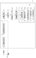
図1は、本発明の第1実施形態に係る位置検出装置を示すブロック図である。
位置検出装置10は、テンプレート画像に近似したマークの位置を入力画像から検出する。位置検出装置10は、ウェハ、ウェハステージ又は大規模集積回路(LSI)等のIC、又はICパッケージ等の電子部品の画像を入力画像として撮影する撮像装置12と、撮像装置12が撮影した入力画像をアナログ信号からデジタル信号に変換するA/Dコンバータ14と、入力画像を一時的に保持する入力画像メモリ16と、予め撮影したテンプレート画像を保持するテンプレート画像保持部18と、位置検出装置10の動作を制御する制御部20と、制御プログラムなどを格納するプログラム格納部22と、演算途中のデータ等を一時的に保持するデータメモリ24と、入力画像からテンプレート画像に近似したマークの位置を検出するための算出処理を行う算出処理部30と、入力画像又はテンプレート画像を表示する表示装置70と、例えばCPU等の制御部20、例えばROM等のプログラム格納部22、例えばRAM等のデータメモリ24、算出処理部30及び表示装置70を接続して各装置間のデータを伝送するバス(BUS)72とを有する。
【0041】
テンプレート画像保持部18は、例えばハードディスク等の記憶装置である。テンプレート画像保持部18は、テンプレート画像のデジタルデータを保持するのが好ましい。また、テンプレート画像保持部18は、テンプレート画像を所定の位置を基準として周波数成分に変換した場合の位相成分を周波数に対応づけて記憶してもよい。テンプレート画像保持部18が保持するテンプレート画像は、一辺がそれぞれ2のn乗(nは正の整数)の画素数を持つのが好ましい。
【0042】
図2は、図1に示した算出処理部30を示すブロック図である。
算出処理部30は、入力画像分割手段32と、比較領域選択手段34と、補正手段36と、変換手段38と、帯域抽出フィルタ40と、位相差算出手段42と、マーク位置検出手段50とを有する。
【0043】
入力画像分割手段32は、入力画像を分割する。入力画像分割手段32は、予備領域がテンプレート画像よりも小さくなるように入力画像を分割するのが好ましい。また、入力画像分割手段32は、分割された各予備領域が、互いに重複しないように入力画像を分割してよい。
【0044】
比較領域選択手段34は、入力画像から、テンプレート画像と実質的に等しい大きさの比較領域を選択する。比較領域選択手段34は、入力画像分割手段32が分割した入力画像の各予備領域を所定の位置にそれぞれ含むように比較領域を選択するのが好ましい。比較領域選択手段34は、各予備領域が比較領域の中心に位置するように比較領域を選択するのが好ましい。また、比較領域選択手段34は、入力画像から複数の比較領域を選択してよい。
【0045】
補正手段36は、入力画像の画素値を補正する。比較領域選択手段34が入力画像から比較領域を選択した場合、補正手段36は、比較領域の端部の画素値が実質的に等しくなるように、比較領域の画素値を補正する。補正手段36は、テンプレート画像の画素値を補正してもよい。
【0046】
変換手段38は、入力画像中の所定の位置を基準として、入力画像を周波数成分に変換する。変換手段38は、フーリエ変換により入力画像を周波数成分に変換してよい。変換手段38は、2次元離散フーリエ変換により入力画像を周波数成分に変換するのが好ましい。2次元離散フーリエ変換は高速フーリエ変換であってよい。本実施形態において、変換手段38は、高速フーリエ変換により入力画像を周波数成分に変換する。
【0047】
比較領域選択手段34が入力画像から比較領域を選択した場合、変換手段38は、比較領域における所定の位置を基準として、その比較領域を周波数成分に変換する。この場合、変換手段38は、テンプレート画像中の基準となる所定の位置に対応する座標を比較領域における所定の位置として、比較領域を周波数成分に変換するのが好ましい。比較領域選択手段34が入力画像から複数の比較領域を選択した場合、変換手段38は、複数の比較領域をそれぞれ周波数成分に変換する。
また同様に、変換手段38は、テンプレート画像中の所定の位置を基準として、テンプレート画像を周波数成分に変換してよい。本実施形態において、変換手段38は、高速フーリエ変換によりテンプレート画像を周波数成分に変換する。
【0048】
帯域抽出フィルタ40は、入力画像の周波数成分から、所定の帯域の周波数成分を抽出する。本実施形態において、帯域抽出フィルタ40は、所定の周波数以下の周波数成分を抽出する低域抽出フィルタである。帯域抽出フィルタ40は、入力画像の周波数成分から、所定の周波数帯域の周波数成分の位相成分のみを抽出してもよい。
【0049】
また、他の例において、帯域抽出フィルタ40は、テンプレート画像を周波数成分に変換した場合の振幅に基づいて、抽出すべき位相成分差の周波数帯域を選択してもよい。例えば、帯域抽出フィルタ40は、テンプレート画像の周波数成分の振幅が大きい順に所定の数の周波数帯域を選択してもよい。また、例えば、帯域抽出フィルタ40は、テンプレート画像の振幅が所定の値以上である周波数帯域を選択してもよい。帯域抽出フィルタ40は、入力画像の周波数成分から、このようにして選択した周波数帯域の周波数成分の位相成分のみを抽出してよい。この場合、帯域抽出フィルタ40は、テンプレート画像のマークの形状に応じて抽出すべき周波数帯域を選択するので、位相インパルス応答関数の精度を向上できる。このように、帯域抽出フィルタ40は、所定の周波数以下の周波数成分のみを抽出する低域通過フィルタに限られない。また、この場合、テンプレート画像保持部18は、帯域抽出フィルタ40が選択した周波数帯域のテンプレート画像の周波数成分を当該周波数帯域に対応づけて保持してもよい。テンプレート画像保持部18は、帯域抽出フィルタ40が選択した周波数帯域のテンプレート画像の周波数成分の位相成分のみを当該周波数帯域に対応づけて保持してもよい。
【0050】
位相差算出手段42は、入力画像の周波数成分の位相成分とテンプレート画像の周波数成分の位相成分との位相成分差を周波数ごとに算出する。比較領域選択手段34が入力画像から複数の比較領域を選択した場合、位相差算出手段42は、比較領域ごとにテンプレート画像の位相成分との位相成分差を算出する。位相差算出手段42は、テンプレート画像の周波数成分を基準とした入力画像の周波数応答関数に基づいて、位相成分差を算出するのが好ましい。
【0051】
マーク位置検出手段50は、位相差算出手段42が算出した位相成分差に基づいて、入力画像中のマークの位置を検出する。マーク位置検出手段50は、逆変換手段52と、座標検出手段54と、比較領域検出手段56と、マーク判断手段58とを有する。
【0052】
逆変換手段52は、位相差算出手段42が算出した位相成分差を変換して位相インパルス応答関数を算出する。逆変換手段52は、フーリエ逆変換により位相インパルス応答関数を算出してよい。逆変換手段52は、2次元離散フーリエ逆変換により位相インパルス応答関数を算出するのが好ましい。2次元離散フーリエ逆変換は、高速フーリエ変換であってよい。本実施形態において、逆変換手段52は、高速フーリエ逆変換により位相インパルス応答関数を算出する。
【0053】
座標検出手段54は、所定の条件を満たす位相インパルス応答関数値を与える座標を入力画像から検出する。比較領域選択手段34が入力画像から複数の比較領域を選択した場合、比較領域検出手段56は、所定の条件を満たす位相インパルス応答関数値を与える座標を含む比較領域を検出する。
【0054】
マーク判断手段58は、比較領域における位相インパルス応答関数値を所定の閾値と比較することにより、マークが当該比較領域に含まれるか否かを判断する。マーク判断手段58は、比較領域における位相インパルス応答関数値を所定の閾値と比較して、位相インパルス応答関数値が閾値よりも大きいときに、マークが当該比較領域に含まれると判断してもよい。マーク判断手段58が複数の比較領域の全てにマークが含まれないと判断した場合、入力画像分割手段32は、異なる位置で再度予備領域を分割してもよい。
【0055】
マーク判断手段58が複数の比較領域の全てにマークが含まれないと判断した場合、マーク判断手段58は、入力画像にマークが含まれないことを制御部20に通知する。これにより、入力画像にマークが含まれない場合に、誤った位置をマークの位置と判断して、ウェハへの処理を行うのを防ぐことができる。
【0056】
また、他の例において、座標検出手段54は、比較領域における位相インパルス応答関数値のうち、所定の領域における位相インパルス応答関数値のみを抽出する手段と、抽出した位相インパルス応答関数値から所定の条件を満たす位相インパルス応答関数値を選択する手段とをさらに有してもよい。この場合、座標検出手段54は、選択した位相インパルス応答関数値を与える座標を検出する。ここで、所定の領域とは、例えば比較領域において、補正手段36による補正の影響を受けていない領域のことをいう。
【0057】
図3は、本実施形態における位置検出装置10が入力画像からテンプレート画像に近似したマークの位置を検出するステップを示すフローチャートである。
まず、入力画像分割手段32は、入力画像を分割して予備領域を形成する(S110)。入力画像がテンプレート画像と実質的に等しい大きさの場合、このステップは省略してよい。
【0058】
次に、比較領域選択手段34は、各予備領域を所定の位置にそれぞれ含むようにして、テンプレート画像と実質的に同じ大きさの比較領域を入力画像から選択する(S120)。補正手段36は、比較領域の端部の画素値が実質的に等しくなるように、比較領域の画素値を補正する(S130)。変換手段38は、高速フーリエ変換により比較領域を周波数成分に変換する(S140)。
【0059】
本実施形態において、補正手段36は、ステップ130において、比較領域の端部の画素値が実質的に等しくなるように、テンプレート画像の画素値を補正してもよい。また、変換手段38は、ステップ140において、高速フーリエ変換によりテンプレート画像を周波数成分に変換してもよい。他の例において、テンプレート画像保持部18は、予め画素値が補正され、周波数成分に変換されたテンプレート画像のデータを保持していてもよい。
【0060】
位相差算出手段42は、比較領域の周波数成分の位相成分とテンプレート画像の周波数成分の位相成分との位相成分差を周波数ごとに算出する(S150)。帯域抽出フィルタ40は、位相差算出手段42が算出した位相成分差のうち、所定の周波数帯域以下の周波数成分の位相成分差のみを抽出する(S160)。逆変換手段52は、位相差算出手段42が算出した位相成分差を変換して位相インパルス応答関数を算出する。(S170)。マーク位置検出手段50は、位相インパルス応答関数に基づいて、入力画像中のマークの位置を検出する(S180)。
【0061】
以下に、図3のフローチャートに示した各ステップを詳細に説明する。
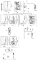
図4は、本実施形態における位置検出装置10が入力画像からテンプレート画像に近似したマークの位置を検出する処理の第1実施例を示す模式図である。
【0062】
本実施例において、入力画像110はテンプレート画像100と実質的に等しい大きさである。テンプレート画像100はマーク102を含む。入力画像110はテンプレート画像100に含まれるマーク102に近似したマーク112を含む。
【0063】
補正手段36は、入力画像110の上端と下端の画素値及び左端と右端の画素値がそれぞれ実質的に等しくなるように入力画像110に2次元の窓関数を適用する。補正手段36は、コサイン・テーパ窓(Tukey窓)を用いて入力画像110の画素値を補正するのが好ましい。本実施形態において、補正手段36は、矩形線対称の2次元コサイン・テーパ窓を用いて入力画像110の画素値を補正する。ここで、矩形線対称の2次元コサイン・テーパ窓とは、例えば窓のサイズをQ×Rとしたときに、窓の中央の矩形領域0≦|q|≦(1−α)Q/2かつ0≦|r|≦(1−α)R/2で振幅1.0となり、この矩形領域の外側の窓の端に近づくに従って振幅が余弦波状に減衰してほぼゼロとなるように画素値を補正する窓関数である。補正手段36は、αの値を調整して矩形領域のサイズを設定するのが好ましい。補正手段36は入力画像と同様に、テンプレート画像の画素値を補正するのが好ましい。
【0064】
このように、補正手段36が入力画像110の端部の画素値が等しくなるように画素値を補正するので、変換手段38が入力画像110を周波数成分に変換する際に、入力画像110における画素値を連続的に変化させることができ、画素値の不連続から生じるスプリアスを減少することができる。
【0065】
変換手段38は、テンプレート画像100及び入力画像110をm軸及びn軸の原点(0,0)を基準として、それぞれ高速フーリエ変換(DFT)により周波数成分に変換する。本実施例において、変換手段38は、次式によりテンプレート画像を高速フーリエ変換する。
【数1】

【0066】
テンプレート画像の高速フーリエ変換T(k,l)及び入力画像の高速フーリエ変換X(k,l)は、それぞれグラフ120及びグラフ122に示されるように周波数に対する振幅及び位相成分で表される。位相差算出手段42は、テンプレート画像の高速フーリエ変換T(k,l)の位相成分と入力画像の高速フーリエ変換X(k,l)の位相成分との位相成分差を算出する。グラフ124は、位相差算出手段42が算出した位相成分差を示す。位相差算出手段42は、次式により、入力画像の高速フーリエ変換X(k,l)とテンプレート画像の高速フーリエ変換T(k,l)との周波数応答関数H(k,l)を算出する。
【数2】
位相差算出手段42は、周波数応答関数H(k,l)から位相成分θH(k,l)を抽出する。ここで、ARG[H(k,l)]は位相成分の主値をあらわす。
【数3】
![]()
【数4】
![]()
【0068】
逆変換手段52は、位相成分差のみを変換した位相インパルス応答関数に基づいて入力画像からマークの位置を検出するので、入力画像の輝度分布の変化やマークの変形の影響を最小限にして精度よく入力画像からマークの位置を検出できる。
【0069】
座標検出手段54は、位相インパルス応答関数のピークを、例えば、入力画像中で、位相インパルス応答関数値が最大となる座標を所定の条件を満たす座標として検出してもよい。また、座標検出手段54は、インパルス応答関数値の絶対値が最大である座標を検出してもよい。
【0070】
座標検出手段54は、各位相インパルス応答関数値が正であるか負であるかを判断する手段をさらに有してもよい。例えば座標検出手段54が、位相インパルス応答関数の絶対値が最大である座標における位相インパルス応答関数が負であると判断した場合、座標検出手段54は、位相インパルス応答関数と所定値との差の絶対値が最大である座標を検出してもよい。また、座標検出手段54は、位相インパルス応答関数が極値である座標を検出してもよい。
【0071】
座標検出手段54が各位相インパルス応答関数値が正であるか負であるかを判断する手段を有すれば、例えば、入力画像のマークが反転して位相インパルス応答関数の値が負となる場合であっても、入力画像中のマークの位置を正確に検出することができる。
【0072】
図5は、位相インパルス応答関数がテンプレート画像におけるマークと入力画像におけるマークのずれを表すことを示す模式図である。
図5(a)は、テンプレート画像100を示す。図5(b)は、入力画像110を示す。図5(c)は、位相インパルス応答関数を示す。位相インパルス応答関数は、テンプレート画像100中のマーク102を基準とした場合の入力画像110中のマーク112の位置を示す座標において、ピークを有する。位相インパルス応答関数のピークは、図5(b)に示すように、テンプレート画像100と入力画像110とのそれぞれに含まれる基準点を一致させて重ねた場合の、テンプレート画像100のマーク102からの入力画像110のマーク112のずれ量と等しい。
【0073】
図5(d)及び5(e)は、入力画像110におけるマーク112の位置がテンプレート画像100におけるマーク102の位置よりも基準点に近い位置にある場合のテンプレート画像100及び入力画像110をそれぞれ示す。この場合、図5(f)に示すように、位相インパルス応答関数のピークの座標は負のベクトルを持つ。座標検出手段54は、テンプレート画像100におけるマーク102の位置と、検出された位相インパルス応答関数のピークの座標とに基づいて位相インパルス応答関数のベクトルの正負を判断する。位置検出装置10は、基準点に近い位置にマーク102を含むようにテンプレート画像100を選択する手段をさらに備えてもよい。
【0074】
図6は、本実施形態における位置検出装置10が入力画像からテンプレート画像に近似したマークの位置を検出する処理の第2実施例を示す模式図である。
本実施例において、入力画像110はテンプレート画像100と実質的に等しい大きさである。また、テンプレート画像100はマーク102を含む。入力画像110はテンプレート画像100に含まれるマーク102に近似したマーク112を含む。
【0075】
本実施例においては、変換手段38は、予めテンプレート画像を周波数成分に変換する。その後、テンプレート画像保持部18は、テンプレート画像の位相成分を各周波数に対応づけて保持する。位置検出装置10は、外部装置により予め周波数成分に変換されたテンプレート画像の位相成分を周波数に対応づけたデータを入力し、テンプレート画像保持部18に保持させてもよい。
【0076】
変換手段38は、第1実施例と同様に、入力画像を周波数成分に変換する。位相差算出手段42は、テンプレート画像保持部18が保持するテンプレート画像の位相成分と入力画像の位相成分との位相成分差を算出する。逆変換手段52は、位相差算出手段42が算出した位相成分差を位相インパルス応答関数に変換する。
【0077】
図7は、本実施形態における位置検出装置10が入力画像からテンプレート画像に近似したマークの位置を検出する処理の第3実施例を示す模式図である。
本実施例において、入力画像110がテンプレート画像100よりも大きい場合に、位置検出装置10が入力画像からマークの位置を検出する処理を説明する。
【0078】
本実施例において、例えば、入力画像分割手段32は、予備領域i1〜i16がテンプレート画像よりも小さくなるように入力画像110を分割する。比較領域選択手段34は、予備領域i1〜i16をそれぞれ中心に含むように、比較領域114を選択する。
【0079】
比較領域選択手段34はさらに、比較領域の画素数を調整する手段を有してもよい。比較領域選択手段34は、例えば予備領域i1を含む領域を選択する場合は、画素値がゼロの画素を付加して比較領域の画素数をテンプレート画像の画素数と同じにする。比較領域選択手段34が、テンプレート画像と実質的に等しい大きさの選択領域を選択するので、変換手段38は、各選択領域をフーリエ変換により周波数成分に変換することができる。
【0080】
また、比較領域選択手段34は、一辺がそれぞれ2のm乗(mは正の整数)の画素数を持つように比較領域を選択するのが好ましい。この場合も比較領域選択手段34の画素数を調整する手段は、選択する比較領域一辺がそれぞれ2のm乗(mは正の整数)の画素数を持つように、画素値がゼロの画素を付加して比較領域の画素数を調整する。
【0081】
比較領域選択手段34が一辺がそれぞれ2のm乗となるように比較領域を選択するので、変換手段38は、各比較領域を高速フーリエ変換により周波数成分に変換できる。そのため、算出処理部30は、より迅速に入力画像からマークの位置を検出することができる。
【0082】
補正手段36は、第1実施例と同様に矩形線対称の2次元コサイン・テーパ窓を用いて、比較領域の上端と下端の画素値及び左端と右端の画素値がそれぞれ実質的に等しくなるように比較領域の画素値を補正する。この場合、補正手段36は、矩形領域が予備領域i1〜i16よりも大きくなるようにαの値を調整するのが好ましい。さらに、補正手段36は、選択された比較領域に画素値がゼロの画素が付加されている場合は、付加された画素が矩形領域に含まれないようにαの値を調整するのが好ましい。また、補正手段36は、窓のサイズが比較領域と実質的に等しい大きさになるようにQ及びRの値を設定する。補正手段36が、付加された画素が矩形領域に含まれないようにαの値を調整するので、比較領域に画素値がゼロの画素を付加した場合でも、画像の連続性を保つことができる。補正手段36は、比較領域と同様に、テンプレート画像の上端と下端の画素値及び左端と右端の画素値がそれぞれ実質的に等しくなるように、テンプレート画像の画素値を補正してもよい。
【0083】
ここで、比較領域選択手段34がテンプレート画像よりも小さい予備領域を含むように各比較領域を選択するので、入力画像はオーバーラップして比較領域に分割されることになる。そのため、比較領域選択手段34は、ある比較領域においてマークが分断されていても、他の比較領域においてマーク全体が含まれるように入力画像を分割することができる。また、比較領域選択手段34は、ある比較領域においてマークが端部に位置している場合であっても、他の比較領域においてマークが中央部に位置するように入力画像を分割することができる。そのため、補正手段36が比較領域の端部の画素値を補正しても、マークが中央部に位置する比較領域における位相インパルス応答関数を用いて、入力画像からマークの位置を正確に検出することができる。
【0084】
変換手段38は、第1実施例と同様に、テンプレート画像100及び比較領域114を周波数成分に変換する。位相差算出手段42は、テンプレート画像の位相成分と入力画像の位相成分との位相成分差を算出する。本実施形態において、帯域抽出フィルタ40は、周波数k=56以下の周波数成分のみの位相成分を抽出する。
【0085】
他の例において、帯域抽出フィルタ40はテンプレート画像100及び比較領域の周波数成分のうち所定の周波数以下の周波数成分のみをそれぞれ抽出し、位相差算出手段42は、帯域抽出フィルタ40が抽出したテンプレート画像及び比較領域の周波数成分の位相成分の位相成分差を算出してもよい。
【0086】
帯域抽出フィルタ40が所定の周波数以下の周波数成分のみを抽出するため、マーク以外の、例えば回路パターン等の形状により生じた周波数成分の影響を除去することができる。また、高い周波数を有し、ランダムに発生する雑音を除去することができるため、位相インパルス応答関数の精度を向上できる。
【0087】
逆変換手段52は、位相差算出手段42が算出した位相成分差をインパルス応答関数に変換する。比較領域選択手段34が比較領域の画素数が一辺がそれぞれ2のm乗となるように比較領域を選択するので、逆変換手段52は、高速フーリエ逆変換により位相インパルス応答関数を算出できる。そのため、算出処理部30は、より迅速に入力画像からマークの位置を検出することができる。
【0088】
座標検出手段54は、選択された比較領域114において位相インパルス応答関数値が最大となる座標を検出する。比較領域検出手段56は、複数の比較領域における位相インパルス応答関数値のうち、最大値を持つ位相インパルス応答関数を含む比較領域を検出する。マーク判断手段58は、比較領域検出手段56が検出した比較領域における位相インパルス応答関数値の最大値を所定値と比較する。そして、比較領域検出手段56は、位相インパルス応答関数値の最大値が所定値より大きい場合にマーク112が当該比較領域に含まれると判断する。
【0089】
比較領域検出手段56は、位相インパルス応答関数値の最大値が所定値より小さい場合には、マーク112が当該比較領域に含まれないと判断する。この場合、入力画像分割手段32は、入力画像110を最初の予備領域とは異なる範囲で予備領域を分割してもよい。位置検出装置10は、同様の処理を繰り返し、位相インパルス応答関数値の最大値が所定値より大きくなる座標を検出する。位相インパルス応答関数値が所定値より大きくなる座標が検出できない場合は、座標検出手段54は、制御部20に入力画像110中にマークが含まれないことを通知する。
【0090】
逆変換手段52は、位相成分差のみを変換した位相インパルス応答関数に基づいて入力画像からマークの位置を検出するので、入力画像の輝度分布の変化やマークの変形の影響を最小限にして精度よく入力画像からマークの位置を検出できる。
【0091】
他の例において、座標検出手段54は、位相インパルス応答関数を示す画像から所定の領域のみを選択してもよい。本実施例においては、補正手段36が比較領域の端部の画素値を補正しているため、比較領域の端部における画素変化により生じる位相インパルス応答関数値のピークは信頼性が低い。従って、座標検出手段54は、補正手段36が比較領域に補正を施す領域に基づいて、位相インパルス応答関数値を示す画像から信頼性の高いピークを与える領域を選択する。座標検出手段54は、このようにして選択した領域を他の比較領域から選択した領域と合成して入力画像と実質的に等しい大きさの位相インパルス応答関数を示す画像を形成してもよい。この場合、座標検出手段54は、合成した位相インパルス応答関数を示す画像から、位相インパルス応答関数値が最大となる座標を検出する。座標検出手段54が、位相インパルス応答関数を示す画像から所定の領域を選択して、選択した領域から位相インパルス応答関数値が最大となる座標を検出するので、入力画像から効率よくマークの位置を検出することができる。
【0092】
図8は、位置検出装置に含まれる算出処理部30の他の例を示すブロック図である。
算出処理部30は、入力画像分割手段32と、比較領域選択手段34と、補正手段36と、変換手段38と、帯域抽出フィルタ40と、位相差算出手段42と、マーク位置検出手段50と、逆数算出手段144と、畳込み積分画像形成手段146とを有する。図2に示した構成要素と同一の符号を持つ構成要素は、図2に示した算出処理部30における構成要素と同様の機能を有する。逆数算出手段138は、テンプレート画像の周波数成分の逆数を求める。畳込み積分画像形成手段146は、テンプレート画像の逆周波数特性を持つテンプレート逆画像と入力画像との畳込み積分画像を形成する。
【0093】
次に、本実施例において、算出処理部30がテンプレート逆画像を形成する手順を示す。まず、補正手段36は、テンプレート画像保持部18に保持されたテンプレート画像の端部の画素値を補正する。変換手段38は、テンプレート画像の画素値を高速フーリエ変換により周波数成分に変換する。逆数算出手段138は、変換したテンプレート画像の周波数成分の逆数を算出する。逆変換手段52は、逆数算出手段138が算出した逆数を高速フーリエ逆変換してテンプレート逆画像を形成する。
【0094】
テンプレート画像保持部18は、テンプレート逆画像を記憶する。畳込み積分画像形成手段146は、テンプレート画像保持部18に保持されたテンプレート逆画像と入力画像との畳込み積分画像を形成する。変換手段38は、畳込み画像を、畳込み画像中の所定の位置を基準として、畳込み画像を周波数成分に変換する。位相差算出手段42は、変換手段38が変換した畳込み画像の位相成分を位相成分差として算出する。逆変換手段52は、第1実施例と同様に、位相差算出手段42が算出した位相成分差を位相インパルス応答関数に変換する。
【0095】
逆変換手段52は、位相成分差のみを変換した位相インパルス応答関数に基づいて入力画像からマークの位置を検出するので、入力画像の輝度分布の変化やマークの変形の影響を最小限にして精度よく入力画像からマークの位置を検出できる。
【0096】
図9は、本発明の第2実施形態に係る電子部品搬送装置を示すブロック図である。
電子部品搬送装置200は、例えば、大規模集積回路(LSI)等のIC、又はICパッケージ等の電子部品の製造工程において、これらの電子部品を次の工程を行う装置に搬送する。また、電子部品搬送装置200は、電子部品の製造工程において、電子部品の性能を試験するために電子部品をテスタまで搬送したり、試験が終了した電子部品をもとのトレイに戻したりする。
【0097】
電子部品搬送装置200は、マークの位置を入力画像から検出する位置検出装置10と、位置検出装置10により検出されたマークの位置に基づいて、電子部品を吸着し、電子部品を移動する電子部品移動手段202とを有する。位置検出装置10は、第1実施形態において図1から図8を参照して説明したのと同様の構成及び機能を有する。電子部品移動手段202は、電子部品を保持する手段と、電子部品を移動する手段とを有するのが好ましい。
【0098】
本実施形態において、電子部品搬送装置200は、位置検出装置10を有するので、位相インパルス応答関数に基づいて入力画像からマークの位置を検出する。そのため、入力画像の輝度分布の変化やマークの変形の影響を最小限にして精度よく入力画像からマークの位置を検出でき、電子部品の搬送を精度よく迅速に行うことができる。
【0099】
図10は、本発明の第3実施形態に係る電子ビーム露光装置300の構成図である。
電子ビーム露光装置300は、電子ビームによりウェハ350に所定の露光処理を施すための露光部302と、露光部302の各構成の動作を制御する制御系360と、位置検出装置10とを備える。位置検出装置10は、第1実施形態において図1から図8を参照して説明したのと同様の構成及び機能を有する。
【0100】
露光部302は、筐体304内部で、電子ビームを発生し、電子ビームの断面形状を所望に整形する電子ビーム整形手段310と、電子ビーム整形手段310から照射された電子ビームを、ウェハ350に照射するか否かを切替える照射切替手段330と、ウェハ350に転写されるパターンの像の向き及びサイズを調整するウェハ用投影系340とを含む電子光学系を備える。また、露光部302は、ウェハ350を載置するウェハステージ352と、ウェハステージ352を駆動するウェハステージ駆動部354とを含むステージ系を備える。本実施形態において、ウェハ350又はウェハウェハステージ352のいずれか一方に、ウェハの位置を検出するためのテンプレート画像に近似したマークが設けられる。
【0101】
電子ビーム照射系310は、電子ビームを発生させる電子銃312と、電子ビームを通過させることにより、断面形状を整形する矩形形状の開口部を有すると、電子ビームを収束し、焦点位置を調整する第1電子レンズ316と、第1整形部材314を通過した電子ビームを偏向する整形偏向部318と、第2整形部材320とを有する。整形偏向部318は、整形偏向部318により偏向された電子ビームを、第2整形部材320に対して略垂直方向に偏向する手段を更に有してもよい。図10において、電子銃312が発生した電子ビームが、電子光学系により偏向されない場合の電子ビームの光軸を、一点鎖線Aで表現する。
【0102】
照射切替手段330は、電子ビームを偏向させることにより、電子ビームをウェハ350に照射するか否かをそれぞれ切替える複数のブランキング電極アレイ332と、電子ビームを収束し、焦点を調整する第2電子レンズ334と、電子ビームを通過させる開口部を含み、ブランキング電極アレイ332で偏向された電子ビームを遮蔽する電子ビーム遮蔽部材336とを有する。電子ビーム遮蔽部材336は、円形の開口(ラウンドアパーチャ)を有する。ブランキング電極アレイ332は、電子ビームを高速に同期してオン/オフする。具体的には、電子ビームを電子ビーム遮蔽部材336のラウンドアパーチャの外側に当たるように偏向する機能を有する。すなわち、ブランキング電極アレイ332は、電子ビームの進行方向に対して電子ビーム遮蔽部材336から下流に電子ビームが進行するのを防ぐことができる。
【0103】
ブランキング電極アレイ332は、電子ビーム露光装置300がウェハ350に転写するパターンを変更するとき、又はパターンを露光するウェハ350の領域を変更するとき等、電子ビーム露光装置300がウェハ350にパターンを露光する必要がないときは、電子ビーム遮蔽部材336から下流に電子ビームが進行しないように電子ビームを偏向するのが望ましい。
【0104】
ウェハ用投影系340は、第2整形部材120で形成されたパターンに対応する、ウェハ350に転写されるパターン像の縮小率を調整する第3電子レンズ342と、ウェハ350上の所定の領域に電子ビームが照射されるように、電子ビームを偏向する偏向部344と、対物レンズとして機能する第4電子レンズとを有する。
【0105】
制御系360は、統括制御部370及び個別制御部380を備える。個別制御部380は、電子ビーム制御部382と、電子レンズ制御部384と、整形偏向制御部386と、ブランキング電極アレイ制御部388と、偏向制御部390と、ウェハステージ制御部392とを有する。統括制御部370は、例えばワークステーションであって、個別制御部380に含まれる各制御部を統括制御する。
【0106】
電子ビーム制御部382は、電子銃312を制御する。電子レンズ制御部384は、第1電子レンズ316、第2電子レンズ334、第3電子レンズ342及び第4電子レンズ346に供給する電流を制御する。整形偏向制御部386は、整形偏向部318を制御する。ブランキング電極アレイ制御部388は、ブランキング電極アレイ332に含まれる偏向電極に印加する電圧を制御する。偏向制御部390は、偏向部344を制御する。ウェハステージ制御部392は、位置検出装置10が検出したマークの位置に基づいて、ウェハステージ駆動部354を制御し、ウェハステージ352を所定の位置に移動させる。
【0107】
図10を参照して、本実施形態に係る電子ビーム露光装置300の動作を説明する。ウェハステージ352上には、露光処理が施されるウェハ350が載置される。電子銃312が安定した電子ビームを発生するには所定の時間がかかるので、本実施形態において、電子銃312は露光処理期間にわたって常に電子ビームを発生する。図中、実線は電子ビームの照射経路を、一点鎖線は電子ビームの光軸をそれぞれ示す。
【0108】
位置検出装置10の撮像装置12は、ウェハ350又はウェハステージ352に設けられたマークの画像を入力画像として撮像する。位置検出装置10は、第1実施形態において説明した位相インパルス応答関数を用いて入力画像からマークの位置を検出する。そして、ウェハステージ制御部392は、位置検出装置10が検出したマークの位置に基づいて、ウェハステージ駆動部354を制御し、ウェハステージ352を移動させて、ウェハ350の露光されるべき領域が電子ビームの光軸近傍に位置するようにする。
【0109】
ウェハ350への露光の開始前において、第2整形部材120の開口を通過した電子ビームがウェハ350に照射されないように、ブランキング電極アレイ制御部388が、ブランキング電極アレイ332を制御する。
【0110】
電子レンズ制御部384は、電子銃312が発生した電子ビームの焦点位置をウェハ350に合わせるように第1電子レンズ316、第2電子レンズ334、第3電子レンズ342及び第4電子レンズ346に供給する電流を制御する。電子銃312が発生した電子ビームは、第1整形部材314に照射され、整形される。第1整形部材314により整形された電子ビームは第2整形部材320に照射される。電子ビームは、第2整形部材320によりウェハ350に照射すべき所望の形状に成形される。第2整形部材320において成形された電子ビームをウェハ350に照射すべく、ブランキング電極アレイ制御部390は、電子ビームの偏向を停止するように、ブランキング電極アレイ332を制御する。ブランキング電極アレイ制御部388が、ブランキング電極アレイ332による電子ビームの偏向を停止する。そして、ブランキング電極アレイ332により偏向されない電子ビームは、第2電子レンズ334により電子ビーム径を縮小されて、電子ビーム遮蔽部材336に含まれるラウンドアパーチャを通過する。
【0111】
電子ビーム遮蔽部材336を通過した電子ビームは、第3電子レンズ342により、パターン像の縮小率が調整される。それから、電子ビームは、偏向部344により、ウェハ350上の所定の領域に照射されるように偏向される。電子ビームはさらに、第4電子レンズ346によって調整されて、ウェハ350に照射される。
【0112】
所定の露光時間が経過した後、ブランキング電極アレイ制御部390は、電子ビームをウェハ350に照射しないようにすべく、電子ビームを偏向させるように、ブランキング電極アレイ332を制御する。以上のプロセスにより、ウェハ350上の所定の領域に、パターンが露光される。電子ビーム露光装置300は、この露光処理を、繰り返し実行することによって、所望の回路パターンを、ウェハ350に露光することができる。
【0113】
電子ビーム露光装置300は、可変矩形を用いた電子ビーム露光装置であってもよく、また、ブランキング・アパーチャ・アレイ(BAA)・デバイスを用いた電子ビーム露光装置であってもよい。
【0114】
本実施形態において、電子ビーム露光装置300は、位置検出装置10を有するので、位相インパルス応答関数に基づいて入力画像からマークの位置を検出する。そのため、入力画像の輝度分布の変化やマークの変形の影響を最小限にして精度よく入力画像からマークの位置を検出でき、ウェハ350への露光を精度よく迅速に行うことができる。
【0115】
以上、本発明を実施の形態を用いて説明したが、本発明の技術的範囲は上記実施形態に記載の範囲には限定されない。上記実施形態に、多様な変更または改良を加えることができる。そのような変更または改良を加えた形態も本発明の技術的範囲に含まれ得ることが、特許請求の範囲の記載から明らかである。
【0116】
【発明の効果】
上記説明から明らかなように、本発明によれば入力画像の輝度分布の変化やマークの変形の影響を最小限にして精度よく入力画像からマークの位置を検出することができる。
【図面の簡単な説明】
【図1】本発明の第1実施形態に係る位置検出装置を示すブロック図である。
【図2】図1に示した算出処理部を示すブロック図である。
【図3】本実施形態における位置検出装置が入力画像からテンプレート画像に近似したマークの位置を検出するステップを示すフローチャートである。
【図4】本実施形態における位置検出装置10が入力画像からテンプレート画像に近似したマークの位置を検出する処理の第1実施例を示す模式図である。
【図5】位相インパルス応答関数がテンプレート画像におけるマークと入力画像におけるマークのずれを表すことを示す模式図である。
【図6】本実施形態における位置検出装置10が入力画像からテンプレート画像に近似したマークの位置を検出する処理の第2実施例を示す模式図である。
【図7】本実施形態における位置検出装置10が入力画像からテンプレート画像に近似したマークの位置を検出する処理の第3実施例を示す模式図である。
【図8】本実施形態における位置検出装置に含まれる算出処理部の他の例を示すブロック図である。
【図9】本発明の第2実施形態に係る電子部品搬送装置を示すブロック図である。
【図10】本発明の第3実施形態に係る電子ビーム露光装置の構成図である。
【符号の説明】
10…位置検出装置、12…撮像装置、14…A/Dコンバータ、16…入力画像メモリ、18…テンプレート画像保持部、20…制御部、22…プログラム格納部、24…データメモリ、30…算出処理部、32…入力画像分割手段、34…比較領域選択手段、36…補正手段、38…変換手段、40…帯域抽出フィルタ(低域抽出フィルタ)、42…位相差算出手段、50…マーク位置検出手段、52…逆変換手段、54…座標検出手段、56…比較領域検出手段、58…マーク判断手段、144…逆数算出手段、146…畳込み積分画像形成手段、200…電子部品搬送装置、202…電子部品移動手段、300…電子ビーム露光装置、302…露光部、304…筐体、310…電子ビーム整形手段、312…電子銃(電子ビーム発生部)、314…第1整形部材、316…第1電子レンズ、318…整形偏向部、320…第2整形部材、330…照射切替手段、332…ブランキング電極アレイ、334…第2電子レンズ、336…電子ビーム遮蔽部材、340…ウェハ用投影系、342…第3電子レンズ、344…偏向部、346…第4電子レンズ、350…ウェハ、352…ウェハステージ、354…ウェハステージ駆動部、360…制御系、370…統括制御部、380…個別制御部、382…電子ビーム制御部、384…電子レンズ制御部、386…整形偏向制御部、388…ブランキング電極アレイ制御部、390…偏向制御部、392…ウェハステージ制御部[0001]
BACKGROUND OF THE INVENTION
The present invention relates to a position detection apparatus that detects a position of a mark approximate to a template image from an input image, an electronic component transport apparatus having a position detection apparatus, an electron beam exposure apparatus having a position detection apparatus, and a position detection method. In particular, the present invention relates to a position detection device that accurately detects the position of a mark from an input image while minimizing the influence of changes in the luminance distribution of the input image and the deformation of the mark, an electronic component conveying device having the position detection device, and position detection. The present invention relates to an electron beam exposure apparatus having a device and a position detection method.
[0002]
[Prior art]
In a manufacturing process of a large scale integrated circuit (LSI), it is necessary to repeat a process of exposing a fine circuit pattern on a wafer substrate such as a semiconductor, a process of forming various films, and the like. In order to give the LSI a function as designed, the wafer substrate must be aligned to an accurate position for each process. Therefore, the wafer substrate is aligned by providing a mark on the wafer substrate in advance and observing the position of the mark. Conventionally, pattern matching processing is performed in which the luminance distribution between a template image and an input image obtained by photographing a wafer substrate is compared to detect the position of a mark in the input image.
[0003]
[Problems to be solved by the invention]
However, when various films are stacked on the wafer substrate, the luminance value may locally change in the vicinity of the mark, and the shape of the mark may be deformed and observed. Further, when the wafer substrate is subjected to chemical mechanical polishing (CMP), the edge of the mark may be lost, and in this case, the mark shape is deformed and observed. Further, the thickness of the underlying layer becomes uneven in the wafer substrate due to the CMP treatment, and when another film is formed thereon, the intensity of the reflected light may locally change due to the difference in film thickness. . In such a case, there is a problem that the wafer substrate cannot be accurately aligned by the conventional pattern matching process using the luminance value.
[0004]
SUMMARY OF THE INVENTION An object of the present invention is to provide a position detection apparatus, an electronic component transport apparatus having a position detection apparatus, an electron beam exposure apparatus having a position detection apparatus, and a position detection method that can solve the above problems. This object is achieved by a combination of features described in the independent claims. The dependent claims define further advantageous specific examples of the present invention.
[0005]
[Means for Solving the Problems]
That is, according to the first aspect of the present invention, a position detection device that detects a position of a mark approximate to a template image from an input image, and converts the template image into a frequency component based on a predetermined position in the template image. A phase difference calculating unit that calculates, for each frequency, a phase component difference between the phase component when the input image is converted to a frequency component with the predetermined position in the input image as a reference, and a phase difference calculating unit And a mark position detecting means for detecting the position of the mark in the input image based on the phase impulse response function obtained by converting the phase component difference calculated by the above.
[0006]
The phase difference calculating means preferably calculates the phase component difference based on the frequency response function of the input image with reference to the template image. The mark position detection means may calculate the phase impulse response function by two-dimensional discrete Fourier inverse transform. The two-dimensional discrete Fourier transform may be a fast Fourier transform.
[0007]
The mark position detecting means has coordinate detecting means for detecting from the input image a coordinate that provides a phase impulse response function value satisfying a predetermined condition, and detects the position of the mark based on the coordinates detected by the coordinate detecting means. Good.
[0008]
The coordinate detection means may detect a coordinate having a maximum phase impulse response function value. The coordinate detection means may detect a coordinate having the maximum absolute value of the impulse response function value. The coordinate detecting means may detect a coordinate having a maximum absolute value of a difference between the phase impulse response function value and a predetermined value. The coordinate detection means may detect coordinates where the phase impulse response function value is an extreme value. The coordinate detecting means may detect a coordinate having a maximum absolute value of a difference between the phase impulse response function value and a predetermined value.
[0009]
The position detection device may further include conversion means for converting the input image into frequency components. The converting means may convert the input image into frequency components by two-dimensional discrete Fourier transform. The two-dimensional discrete Fourier transform may be a fast Fourier transform.
[0010]
The position detection apparatus may further include a comparison region selection unit that selects a comparison region having a size substantially equal to the template image from the input image, and the conversion unit serves as a reference in the template image in the comparison region. The comparison region may be converted into a frequency component by using coordinates corresponding to the predetermined position as a predetermined position serving as a reference in the input image.
[0011]
The comparison area selection unit may select the comparison area from the input image so that the comparison areas overlap each other by a predetermined percentage. Specifically, the position detection device may further include an input image dividing unit that divides the input image into spare regions smaller than the template image, and the comparison region selecting unit includes each spare region at a predetermined position. In this way, the comparison area may be selected.
[0012]
The position detection device may further include a correction unit that corrects the pixel value in the comparison region so that the pixel values at the end portions of the comparison region are substantially equal. The correcting means may correct the pixel value of the template image so that the pixel values at the end portions of the template image are substantially equal. The comparison area selecting means may select the comparison area so that each side has a number of pixels of 2 to the power of m (m is a positive integer). The comparison area selection means may have means for adjusting the number of pixels in the comparison area.
[0013]
The mark position detection unit further includes a comparison region detection unit that detects a comparison region including coordinates that provide a phase impulse response function value satisfying a predetermined condition based on the phase impulse response function obtained by converting the phase component difference. The mark position may be detected based on the position of the comparison area in the input image and the coordinates in the comparison area.
[0014]
The mark position detecting means selects a predetermined area from each comparison area, extracts a phase impulse response function value in the predetermined area, and a phase impulse response function that satisfies a predetermined condition from the extracted phase impulse response function value Means for selecting a value, and coordinates for providing a selected phase impulse response function value may be detected.
[0015]
The mark position detection means compares the phase impulse response function value in the comparison area with a predetermined threshold based on the phase impulse response function obtained by converting the phase component difference in the comparison area, thereby determining whether the mark is included in the comparison area. You may further have the mark judgment means which judges whether or not.
[0016]
The position detection device may further include a low-frequency extraction filter that extracts a phase component of a frequency component equal to or lower than a predetermined band, and the mark position detection unit includes the phase component of the template image extracted by the low-frequency extraction filter and the low frequency The position of the mark in the input image may be detected based on the phase impulse response function obtained by converting the phase component difference with the phase component of the input image extracted by the extraction filter.
[0017]
The position detection device may further include a template image holding unit that holds a phase component at a frequency determined based on an amplitude value when the template image is converted into a frequency component in association with the frequency, and calculates a phase difference. The means includes, among the phase components when the input image is converted to the frequency component, a phase between the phase component of the frequency corresponding to the frequency held by the template image holding unit and the phase component of the template image held by the template image holding unit. The component difference may be calculated for each frequency.
[0018]
The conversion means may convert the template image into a frequency component. The position detection apparatus may further include a template image holding unit that holds the phase component when the template image is converted into the frequency component in association with the frequency. The template image preferably has a number of pixels of which each side is 2 to the power of n (n is a positive integer).
[0019]
The position detection device includes a template image holding unit that holds a template inverse image having an inverse frequency characteristic of the template image, a convolution integration unit that forms a convolution integral image of the template inverse image and the input image, and a convolution image. The image processing apparatus may further include a conversion unit that converts the predetermined position into a frequency component, and the phase difference calculation unit may calculate the phase component of the frequency component of the convolution image as the phase component difference.
[0020]
According to the second aspect of the present invention, there is provided a position detection method for detecting a position of a mark approximate to a template image from an input image, wherein the template image is converted into a frequency component with a predetermined position in the template image as a reference. A phase component difference calculating step for calculating the phase component difference for each frequency between the phase component of the input image and the phase component when the input image is converted into the frequency component with reference to a predetermined position in the input image, and the phase component difference There is provided a position detection method comprising: an inverse conversion step for converting to an impulse response function, and a mark position detection step for detecting the position of the mark in the input image based on the phase impulse response function.
[0021]
The mark position detection step may include an inverse conversion step for converting the phase component difference into a phase impulse response function, and the position of the mark in the input image may be detected based on the phase impulse response function.
[0022]
The inverse transformation step may calculate a phase impulse response function by two-dimensional discrete Fourier inverse transformation. The mark position detecting step may include a coordinate detecting step of detecting from the input image a coordinate that provides a phase impulse response function value satisfying a predetermined condition, and detecting the position of the mark based on the detected coordinate. Good.
[0023]
The coordinate detection step may detect a coordinate having a maximum phase impulse response function value. The coordinate detection step may detect a coordinate having the maximum absolute value of the impulse response function value. The coordinate detection step may detect a coordinate having a maximum absolute value of a difference between the phase impulse response function value and a predetermined value. The coordinate detection step may detect coordinates where the phase impulse response function value is an extreme value. The coordinate detection step may detect a coordinate having a maximum absolute value of a difference between the phase impulse response function value and a predetermined value.
[0024]
The position detection method may further include a conversion step of converting the input image into frequency components. In the conversion step, the input image may be converted into a frequency component by two-dimensional discrete Fourier transform.
[0025]
A comparison region selection step for selecting a comparison region having a size substantially equal to the template image from the input image may be further provided, and the conversion step corresponds to a predetermined position serving as a reference in the template image in the comparison region. The comparison area may be converted into a frequency component with the coordinates to be used as a predetermined position as a reference in the input image.
[0026]
An input image dividing step for dividing the input image into spare regions smaller than the template image may be further provided, and the comparison region selecting step may select the comparison regions so as to include the respective spare regions at predetermined positions.
[0027]
The position detection method may further include a correction step of correcting the pixel value in the comparison region so that the pixel values at the end portions of the comparison region are substantially equal. In the comparison area selection step, the comparison area may be selected so that each side has a number of pixels of 2 to the power of m (m is a positive integer).
[0028]
The mark position detection step further includes a comparison region detection step of detecting a comparison region including a coordinate that provides a phase impulse response function value satisfying a predetermined condition based on the phase impulse response function obtained by converting the phase component difference. In many cases, the position of the mark may be detected based on the position of the comparison area in the input image and the coordinates in the comparison area.
[0029]
The mark position detection step includes a step of selecting a predetermined region from the comparison region, an extraction step of extracting a phase impulse response function value in the predetermined region, and a phase impulse response satisfying a predetermined condition from the extracted phase impulse response function value Selecting a function value, and detecting coordinates that provide the selected phase impulse response function value.
[0030]
In the mark position detection step, based on the phase impulse response function obtained by converting the phase component difference in the comparison area, the phase impulse response function value in the comparison area is compared with a predetermined threshold value to determine whether the mark is included in the comparison area. You may have the mark determination step which determines whether or not.
[0031]
The position detection method may further include a low frequency extraction step for extracting a phase component of a frequency component equal to or lower than a predetermined band, and the mark position detection step includes a phase component of the template image extracted in the low frequency extraction step, and The position of the mark in the input image may be detected based on the phase component difference from the phase component of the input image extracted in the low-frequency extraction step.
[0032]
The position detection method may further include a template frequency holding step for holding a phase component at a frequency determined based on an amplitude value when the template image is converted into a frequency component in association with the frequency. The calculation step includes a phase component of a frequency corresponding to the frequency held in the template frequency holding step and a phase component of the template image held in the template frequency holding step among the phase components when the input image is converted into the frequency component. The phase component difference between and may be calculated for each frequency.
[0033]
The position detection method may further include a conversion step of converting the template image into a frequency component by two-dimensional discrete Fourier transform. The position detection method may further include a template image holding step that holds the phase component in the case where the template image is converted into the frequency component in association with the frequency. The position detection method may further include a step of selecting the template image so that each side of the template image has a number of pixels each having an n power of 2 (n is a positive integer). The position detection method may further include a correction step of correcting the pixel value of the template image so that the pixel values at the end portions of the template image are substantially equal.
[0034]
The position detection method includes a template image holding step for holding a template inverse image having an inverse frequency characteristic of the template image, a convolution integral image forming step for forming a convolution integral image of the template inverse image and the input image, and convolution A conversion step of converting the image into a frequency component with a predetermined position as a reference, and the phase component difference calculation step may calculate a phase component from a reference position in the convolution image as a phase component difference. .
[0035]
In the position detection method, a template image is formed by converting a template image into a frequency component by two-dimensional discrete Fourier transform, obtaining an inverse number of the frequency component of the converted template image, and performing the two-dimensional discrete Fourier transform of the inverse number. An inverse conversion step.
[0036]
According to a third aspect of the present invention, there is provided an electronic component transport apparatus that transports an electronic component having a mark that approximates a template image, the input image capturing unit that captures the mark image as an input image, and the position of the mark. Provided is an electronic component transport device that includes a position detection device that detects an input image and an electronic component moving unit that picks up an electronic component and moves the electronic component based on the position of a mark detected by the position detection device. The position detection device includes a phase component when the template image is converted into a frequency component with a predetermined position in the template image as a reference, and a phase when the input image is converted into a frequency component with the predetermined position in the input image as a reference. A phase difference calculating unit that calculates a phase component difference from the component for each frequency, and a mark that detects the position of the mark in the input image based on a phase impulse response function obtained by converting the phase component difference calculated by the phase difference calculating unit And a position detection means.
[0037]
According to a fourth aspect of the present invention, there is provided an electron beam exposure apparatus for exposing a pattern to an wafer with an electron beam, an electron beam generating unit for generating an electron beam, a wafer stage for mounting the wafer, and the wafer or wafer. An input image imaging unit that is provided on any one of the stages and captures an image of a mark that approximates a template image for detecting the position of the wafer as an input image; and a position detection device that detects the position of the mark from the input image; An electron beam exposure apparatus comprising: The position detection device includes a phase component when the template image is converted into a frequency component with a predetermined position in the template image as a reference, and a phase when the input image is converted into a frequency component with the predetermined position in the input image as a reference. A phase difference calculating unit that calculates a phase component difference from the component for each frequency, and a mark that detects the position of the mark in the input image based on a phase impulse response function obtained by converting the phase component difference calculated by the phase difference calculating unit And a position detection means.
[0038]
The electron beam exposure apparatus may further include wafer stage moving means for moving the wafer stage based on the position of the mark detected by the position detection device.
The above summary of the invention does not enumerate all the necessary features of the present invention, and sub-combinations of these feature groups can also be the invention.
[0039]
DETAILED DESCRIPTION OF THE INVENTION
Hereinafter, the present invention will be described through embodiments of the invention. However, the following embodiments do not limit the claimed invention, and all combinations of features described in the embodiments are the solution of the invention. It is not always essential to the means.
[0040]
FIG. 1 is a block diagram showing a position detection apparatus according to the first embodiment of the present invention.
The
[0041]
The template
[0042]
FIG. 2 is a block diagram showing the
The
[0043]
The input
[0044]
The comparison
[0045]
The correcting
[0046]
The
[0047]
When the comparison
Similarly, the
[0048]
The
[0049]
In another example, the
[0050]
The phase difference calculation means 42 calculates the phase component difference between the phase component of the frequency component of the input image and the phase component of the frequency component of the template image for each frequency. When the comparison
[0051]
The mark
[0052]
The
[0053]
The coordinate
[0054]
The mark determination means 58 determines whether or not the mark is included in the comparison area by comparing the phase impulse response function value in the comparison area with a predetermined threshold value. The
[0055]
When the
[0056]
In another example, the coordinate detecting
[0057]
FIG. 3 is a flowchart illustrating steps in which the
First, the input
[0058]
Next, the comparison
[0059]
In the present embodiment, the
[0060]
The phase difference calculation means 42 calculates the phase component difference between the phase component of the frequency component in the comparison region and the phase component of the frequency component of the template image for each frequency (S150). The
[0061]
Hereinafter, each step shown in the flowchart of FIG. 3 will be described in detail.
FIG. 4 is a schematic diagram illustrating a first example of a process in which the
[0062]
In the present embodiment, the
[0063]
The
[0064]
As described above, the
[0065]
The
[Expression 1]
[0066]
The fast Fourier transform T (k, l) of the template image and the fast Fourier transform X (k, l) of the input image are represented by amplitude and phase components with respect to the frequency as shown in the
[Expression 2]
The phase difference calculating means 42 calculates the phase component θ from the frequency response function H (k, l). H Extract (k, l). Here, ARG [H (k, l)] represents the main value of the phase component.
[Equation 3]
![]()
[Expression 4]
![]()
[0068]
The inverse conversion means 52 detects the position of the mark from the input image based on the phase impulse response function obtained by converting only the phase component difference, so that the influence of the change in the luminance distribution of the input image and the deformation of the mark is minimized and the accuracy is improved. It is possible to detect the mark position from the input image.
[0069]
The coordinate
[0070]
The coordinate detection means 54 may further include means for determining whether each phase impulse response function value is positive or negative. For example, when the coordinate
[0071]
If the coordinate detection means 54 has means for judging whether each phase impulse response function value is positive or negative, for example, when the mark of the input image is inverted and the value of the phase impulse response function becomes negative Even so, the position of the mark in the input image can be accurately detected.
[0072]
FIG. 5 is a schematic diagram showing that the phase impulse response function represents the deviation between the mark in the template image and the mark in the input image.
FIG. 5A shows a
[0073]
5D and 5E show the
[0074]
FIG. 6 is a schematic diagram illustrating a second example of a process in which the
In the present embodiment, the
[0075]
In the present embodiment, the conversion means 38 converts the template image into frequency components in advance. Thereafter, the template
[0076]
The conversion means 38 converts the input image into frequency components as in the first embodiment. The phase difference calculation means 42 calculates the phase component difference between the phase component of the template image held by the template
[0077]
FIG. 7 is a schematic diagram illustrating a third example of a process in which the
In the present embodiment, a process in which the
[0078]
In this embodiment, for example, the input
[0079]
The comparison area selection means 34 may further include means for adjusting the number of pixels in the comparison area. For example, when the region including the spare region i1 is selected, the comparison
[0080]
Further, it is preferable that the comparison
[0081]
Since the comparison
[0082]
As in the first embodiment, the correcting means 36 uses a two-dimensional cosine-tapered window that is symmetrical to the rectangular line so that the pixel values at the upper and lower ends and the pixel values at the left and right ends of the comparison area are substantially equal. The pixel value in the comparison area is corrected. In this case, the
[0083]
Here, since the comparison
[0084]
The conversion means 38 converts the
[0085]
In another example, the
[0086]
Since the
[0087]
The inverse conversion means 52 converts the phase component difference calculated by the phase difference calculation means 42 into an impulse response function. Since the comparison
[0088]
The coordinate
[0089]
The comparison
[0090]
The inverse conversion means 52 detects the position of the mark from the input image based on the phase impulse response function obtained by converting only the phase component difference, so that the influence of the change in the luminance distribution of the input image and the deformation of the mark is minimized and the accuracy is improved. It is possible to detect the mark position from the input image.
[0091]
In another example, the coordinate
[0092]
FIG. 8 is a block diagram illustrating another example of the
The
[0093]
Next, in the present embodiment, a procedure in which the
[0094]
The template
[0095]
The inverse conversion means 52 detects the position of the mark from the input image based on the phase impulse response function obtained by converting only the phase component difference, so that the influence of the change in the luminance distribution of the input image and the deformation of the mark is minimized and the accuracy is improved. It is possible to detect the mark position from the input image.
[0096]
FIG. 9 is a block diagram showing an electronic component carrying apparatus according to the second embodiment of the present invention.
For example, in the manufacturing process of an electronic component such as an IC such as a large scale integrated circuit (LSI) or an IC package, the electronic
[0097]
The electronic
[0098]
In the present embodiment, since the electronic
[0099]
FIG. 10 is a block diagram of an electron
The electron
[0100]
The
[0101]
When the electron
[0102]
The
[0103]
The blanking
[0104]
The
[0105]
The
[0106]
The electron
[0107]
With reference to FIG. 10, the operation of the electron
[0108]
The
[0109]
The blanking electrode
[0110]
The
[0111]
The reduction rate of the pattern image of the electron beam that has passed through the electron
[0112]
After a predetermined exposure time has elapsed, the blanking electrode
[0113]
The electron
[0114]
In this embodiment, since the electron
[0115]
As mentioned above, although this invention was demonstrated using embodiment, the technical scope of this invention is not limited to the range as described in the said embodiment. Various modifications or improvements can be added to the above embodiment. It is apparent from the scope of the claims that the embodiments added with such changes or improvements can be included in the technical scope of the present invention.
[0116]
【The invention's effect】
As is clear from the above description, according to the present invention, the position of the mark can be detected from the input image with high accuracy while minimizing the influence of the change in the luminance distribution of the input image and the deformation of the mark.
[Brief description of the drawings]
FIG. 1 is a block diagram showing a position detection apparatus according to a first embodiment of the present invention.
FIG. 2 is a block diagram showing a calculation processing unit shown in FIG.
FIG. 3 is a flowchart showing steps of detecting a position of a mark approximated to a template image from an input image by the position detection apparatus according to the present embodiment.
FIG. 4 is a schematic diagram illustrating a first example of a process in which the
FIG. 5 is a schematic diagram showing that a phase impulse response function represents a shift between a mark in a template image and a mark in an input image.
FIG. 6 is a schematic diagram illustrating a second example of a process in which the position detection device according to the present embodiment detects a mark position that approximates a template image from an input image.
FIG. 7 is a schematic diagram illustrating a third example of a process in which the
FIG. 8 is a block diagram illustrating another example of a calculation processing unit included in the position detection device according to the present embodiment.
FIG. 9 is a block diagram showing an electronic component transport apparatus according to a second embodiment of the present invention.
FIG. 10 is a block diagram of an electron beam exposure apparatus according to a third embodiment of the present invention.
[Explanation of symbols]
DESCRIPTION OF
Claims (54)
前記入力画像を、前記テンプレート画像より小さい予備領域に分割する入力画像分割手段と、
前記入力画像から、前記予備領域をそれぞれ含むように前記テンプレート画像と実質的に等しい大きさの比較領域を選択して、前記入力画像の一部をオーバーラップして前記比較領域に分割する比較領域選択手段と、
前記テンプレート画像中の所定の位置を基準として前記テンプレート画像を周波数成分に変換した場合の位相成分と、前記入力画像中の所定の位置を基準として前記入力画像を周波数成分に変換した場合の位相成分との位相成分差を周波数ごとに算出する位相差算出手段と、
前記位相差算出手段が算出した前記位相成分差を変換した位相インパルス応答関数に基づいて、前記入力画像中の前記マークの位置を検出するマーク位置検出手段と、
を備えることを特徴とする位置検出装置。A position detection device that detects a position of a mark approximate to a template image from an input image,
Input image dividing means for dividing the input image into preliminary regions smaller than the template image;
A comparison area that selects a comparison area having a size substantially equal to the template image so as to include each of the spare areas from the input image, and overlaps a part of the input image and divides the comparison area into the comparison areas A selection means;
A phase component when the template image is converted into a frequency component with a predetermined position in the template image as a reference, and a phase component when the input image is converted into a frequency component with the predetermined position in the input image as a reference A phase difference calculating means for calculating the phase component difference for each frequency;
Mark position detection means for detecting the position of the mark in the input image based on a phase impulse response function obtained by converting the phase component difference calculated by the phase difference calculation means ;
A position detection device comprising:
前記位相成分差を変換した位相インパルス応答関数に基づいて、所定の条件を満たす位相インパルス応答関数値を与える座標を含む前記比較領域を検出する比較領域検出手段をさらに有し、
前記入力画像における前記比較領域の位置と、前記比較領域中の前記座標とに基づいて、前記マークの位置を検出することを特徴とする請求項12に記載の位置検出装置。The mark position detecting means includes
Based on the phase impulse response function obtained by converting the phase component difference, further comprising a comparison region detection means for detecting the comparison region including coordinates that give a phase impulse response function value satisfying a predetermined condition,
The position detection apparatus according to claim 12, wherein the position of the mark is detected based on the position of the comparison area in the input image and the coordinates in the comparison area.
各前記比較領域から所定の領域を選択して、前記所定の領域における位相インパルス応答関数値を抽出する手段と、
抽出した前記位相インパルス応答関数値から所定の条件を満たす前記位相インパルス応答関数値を選択する手段とをさらに有し、
選択した前記位相インパルス応答関数値を与える座標を検出することを特徴とする請求項12に記載の位置検出装置。The mark position detecting means includes
Means for selecting a predetermined region from each of the comparison regions and extracting a phase impulse response function value in the predetermined region;
Means for selecting the phase impulse response function value satisfying a predetermined condition from the extracted phase impulse response function value;
The position detection apparatus according to claim 12, wherein a coordinate that provides the selected phase impulse response function value is detected.
前記マーク位置検出手段は、前記低域抽出フィルタが抽出した前記テンプレート画像の前記位相成分と前記低域抽出フィルタが抽出した前記入力画像の前記位相成分との位相成分差を変換した位相インパルス応答関数に基づいて、前記入力画像中の前記マークの位置を検出することを特徴とする請求項1から19のいずれかに記載の位置検出装置。A low-frequency extraction filter that extracts the phase component of the frequency component below a predetermined band;
The mark position detection means converts a phase impulse response function obtained by converting a phase component difference between the phase component of the template image extracted by the low-frequency extraction filter and the phase component of the input image extracted by the low-frequency extraction filter. based on the position detecting device according to any one of claims 1 to 19, characterized in that to detect the position of the mark in the input image.
前記位相差算出手段は、前記入力画像を前記周波数成分に変換した場合の前記位相成分のうち、前記テンプレート画像保持手段が保持する前記周波数に対応する周波数の位相成分と、前記テンプレート画像保持手段が保持する前記テンプレート画像の前記位相成分との位相成分差を周波数ごとに算出することを特徴とする請求項1から20のいずれかに記載の位置検出装置。A template image holding means for holding the phase component at a frequency determined based on an amplitude value when the template image is converted into the frequency component in association with the frequency;
The phase difference calculating means includes a phase component of a frequency corresponding to the frequency held by the template image holding means among the phase components when the input image is converted into the frequency component, and the template image holding means. position detecting device according to any one of the phase component difference between the phase components of the template image holding claim 1, characterized in that calculating for each frequency 20.
前記テンプレート逆画像と前記入力画像との畳込み積分画像を形成する畳込み積分手段と、
前記畳込み画像を所定の位置を基準として周波数成分に変換する変換手段とをさらに備え、
前記位相差算出手段は、前記畳込み画像の前記周波数成分の位相成分を前記位相成分差として算出することを特徴とする請求項1から24のいずれかに記載の位置検出装置。Template image holding means for holding a template reverse image having reverse frequency characteristics of the template image;
Convolution integration means for forming a convolution integral image of the template inverse image and the input image;
Conversion means for converting the convolution image into a frequency component based on a predetermined position;
The phase difference calculating means, the position detecting device according to any one of claims 1 to 24, characterized in that to calculate a phase component of the frequency components of the convolution image as the phase component differences.
前記入力画像を、前記テンプレート画像より小さい予備領域に分割する入力画像分割ステップと、
前記入力画像から、前記予備領域をそれぞれ含むように前記テンプレート画像と実質的に等しい大きさの比較領域を選択して、前記入力画像の一部をオーバーラップして前記比較領域に分割する比較領域選択ステップと、
前記テンプレート画像中の所定の位置を基準として前記テンプレート画像を周波数成分に変換した場合の位相成分と、前記入力画像中の所定の位置を基準として前記入力画像を周波数成分に変換した場合の位相成分との位相成分差を周波数ごとに算出する位相成分差算出ステップと、
前記位相成分差を位相インパルス応答関数に変換する逆変換ステップを有し、前記位相インパルス応答関数に基づいて前記入力画像中の前記マークの位置を検出するマーク位置検出ステップと、
を備えることを特徴とする位置検出方法。A position detection method for detecting a mark position approximate to a template image from an input image,
An input image dividing step of dividing the input image into preliminary regions smaller than the template image;
A comparison area that selects a comparison area having a size substantially equal to the template image so as to include each of the spare areas from the input image, and overlaps a part of the input image and divides the comparison area into the comparison areas A selection step;
A phase component when the template image is converted into a frequency component with a predetermined position in the template image as a reference, and a phase component when the input image is converted into a frequency component with the predetermined position in the input image as a reference A phase component difference calculating step for calculating a phase component difference for each frequency, and
A mark position detecting step for detecting the position of the mark in the input image based on the phase impulse response function, including an inverse conversion step for converting the phase component difference into a phase impulse response function ;
A position detection method comprising:
検出された前記座標に基づいて、前記マークの位置を検出することを特徴とする請求項26又は27に記載の位置検出方法。The mark position detection step includes a coordinate detection step of detecting coordinates giving a phase impulse response function value satisfying a predetermined condition from the input image,
28. The position detection method according to claim 26 or 27, wherein the position of the mark is detected based on the detected coordinates.
前記位相成分差を変換した位相インパルス応答関数に基づいて、所定の条件を満たす位相インパルス応答関数値を与える座標を含む前記比較領域を検出する比較領域検出ステップをさらに有し、
前記入力画像における前記比較領域の位置と、前記比較領域中の前記座標とに基づいて、前記マークの位置を検出することを特徴とする請求項37に記載の位置検出方法。The mark position detecting step includes
Based on the phase impulse response function obtained by converting the phase component difference, the method further comprises a comparison region detection step for detecting the comparison region including coordinates that give a phase impulse response function value that satisfies a predetermined condition.
38. The position detection method according to claim 37, wherein the position of the mark is detected based on the position of the comparison area in the input image and the coordinates in the comparison area.
前記比較領域から所定の領域を選択するステップと、
前記所定の領域における位相インパルス応答関数値を抽出する抽出ステップと、
抽出した前記位相インパルス応答関数値から所定の条件を満たす前記位相インパルス応答関数値を選択するステップとをさらに有し、
選択した前記位相インパルス応答関数値を与える座標を検出することを特徴とする請求項37に記載の位置検出方法。The mark position detecting step includes
Selecting a predetermined region from the comparison region;
An extraction step of extracting a phase impulse response function value in the predetermined region;
Selecting the phase impulse response function value satisfying a predetermined condition from the extracted phase impulse response function value,
38. The position detection method according to claim 37, wherein a coordinate that provides the selected phase impulse response function value is detected.
前記マーク位置検出ステップは、前記低域抽出ステップにおいて抽出された前記テンプレート画像の前記位相成分と、前記低域抽出ステップにおいて抽出された前記入力画像の前記位相成分との位相成分差に基づいて、前記入力画像中の前記マークの位置を検出することを特徴とする請求項26から43のいずれかに記載の位置検出方法。A low-frequency extraction step of extracting the phase component of the frequency component below a predetermined band,
The mark position detection step is based on a phase component difference between the phase component of the template image extracted in the low-frequency extraction step and the phase component of the input image extracted in the low-frequency extraction step. position detecting method according to any of claims 26 43, characterized in that for detecting the position of said mark in said input image.
前記位相成分差算出ステップは、前記入力画像を前記周波数成分に変換した場合の前記位相成分のうち、前記テンプレート周波数保持ステップにおいて保持された前記周波数に対応する周波数の位相成分と、前記テンプレート周波数保持ステップにおいて保持された前記テンプレート画像の前記位相成分との位相成分差を周波数ごとに算出することを特徴とする請求項26から44のいずれかに記載の位置検出方法。A template frequency holding step of holding the phase component at a frequency determined based on an amplitude value when the template image is converted into the frequency component in association with the frequency;
The phase component difference calculating step includes a phase component of a frequency corresponding to the frequency held in the template frequency holding step among the phase components when the input image is converted into the frequency component, and the template frequency holding. the position detecting method according to any of claims 26 44, the phase component difference between the phase components and calculates for each frequency of the template image stored in step.
前記テンプレート逆画像と前記入力画像との畳込み積分画像を形成する畳込み積分画像形成ステップと、
前記畳込み画像を所定の位置を基準として周波数成分に変換する変換ステップとをさらに備え、
前記位相成分差算出ステップは、前記畳込み画像中の基準位置からの位相成分を前記位相成分差として算出することを特徴とする請求項26から49のいずれかに記載の位置検出方法。A template image holding step for holding a template inverse image having an inverse frequency characteristic of the template image;
A convolution integral image forming step of forming a convolution integral image of the template inverse image and the input image;
A conversion step of converting the convolution image into a frequency component based on a predetermined position,
The phase component difference calculation step, the position detecting method according to any one of claims 26 49, characterized by calculating a phase component from the reference position in the convolution image as the phase component differences.
変換した前記テンプレート画像の前記周波数成分の逆数を求め、前記逆数を2次元離散フーリエ変換することにより前記テンプレート逆画像を形成する逆変換ステップとを備えることを特徴とする請求項50に記載の位置検出方法。A conversion step of converting the template image into a frequency component by a two-dimensional discrete Fourier transform;
51. The position according to claim 50, further comprising: an inverse transformation step of obtaining an inverse number of the frequency component of the transformed template image and forming the template inverse image by performing a two-dimensional discrete Fourier transform on the inverse number. Detection method.
前記マークの画像を入力画像として撮像する入力画像撮像手段と、
前記入力画像を、前記テンプレート画像より小さい予備領域に分割する入力画像分割手段と、
前記入力画像から、前記予備領域をそれぞれ含むように前記テンプレート画像と実質的に等しい大きさの比較領域を選択して、前記入力画像の一部をオーバーラップして前記比較領域に分割する比較領域選択手段と、
前記マークの位置を前記入力画像から検出する位置検出装置と、
前記位置検出装置により検出された前記マークの位置に基づいて、前記電子部品を吸着し、前記電子部品を移動する電子部品移動手段とを備え、
前記位置検出装置は、
前記テンプレート画像中の所定の位置を基準として前記テンプレート画像を周波数成分に変換した場合の位相成分と、前記入力画像中の所定の位置を基準として前記入力画像を周波数成分に変換した場合の位相成分との位相成分差を周波数ごとに算出する位相差算出手段と、
前記位相差算出手段が算出した前記位相成分差を変換した位相インパルス応答関数に基づいて、前記入力画像中の前記マークの位置を検出するマーク位置検出手段と、
を有することを特徴とする電子部品搬送装置。An electronic component transport apparatus for transporting an electronic component having a mark that approximates a template image,
Input image capturing means for capturing an image of the mark as an input image;
Input image dividing means for dividing the input image into preliminary regions smaller than the template image;
A comparison area that selects a comparison area having a size substantially equal to the template image so as to include each of the spare areas from the input image, and overlaps a part of the input image and divides the comparison area into the comparison areas A selection means;
A position detection device for detecting the position of the mark from the input image;
Based on the position of the mark detected by the position detection device, the electronic component is adsorbed and electronic component moving means for moving the electronic component,
The position detection device includes:
A phase component when the template image is converted into a frequency component with a predetermined position in the template image as a reference, and a phase component when the input image is converted into a frequency component with the predetermined position in the input image as a reference A phase difference calculating means for calculating the phase component difference for each frequency;
Mark position detection means for detecting the position of the mark in the input image based on a phase impulse response function obtained by converting the phase component difference calculated by the phase difference calculation means ;
An electronic component conveying apparatus comprising:
前記電子ビームを発生する電子ビーム発生部と、
前記ウェハを載置するウェハステージと、
前記ウェハ又は前記ウェハステージのいずれか一方に設けられ、ウェハの位置を検出するためのテンプレート画像に近似したマークの画像を入力画像として撮像する入力画像撮像手段と、
前記入力画像を、前記テンプレート画像より小さい予備領域に分割する入力画像分割手段と、
前記入力画像から、前記予備領域をそれぞれ含むように前記テンプレート画像と実質的に等しい大きさの比較領域を選択して、前記入力画像の一部をオーバーラップして前記比較領域に分割する比較領域選択手段と、
前記マークの位置を前記入力画像から検出する位置検出装置とを備え、
前記位置検出装置は、
前記テンプレート画像中の所定の位置を基準として前記テンプレート画像を周波数成分に変換した場合の位相成分と、前記入力画像中の所定の位置を基準として前記入力画像を周波数成分に変換した場合の位相成分との位相成分差を周波数ごとに算出する位相差算出手段と、
前記位相差算出手段が算出した前記位相成分差を変換した位相インパルス応答関数に基づいて、前記入力画像中の前記マークの位置を検出するマーク位置検出手段と、
を有することを特徴とする電子ビーム露光装置。An electron beam exposure apparatus that exposes a pattern on a wafer with an electron beam,
An electron beam generator for generating the electron beam;
A wafer stage on which the wafer is placed;
An input image imaging means that is provided on either the wafer or the wafer stage and captures an image of a mark that approximates a template image for detecting the position of the wafer as an input image;
Input image dividing means for dividing the input image into preliminary regions smaller than the template image;
A comparison area that selects a comparison area having a size substantially equal to the template image so as to include each of the spare areas from the input image, and overlaps a part of the input image and divides the comparison area into the comparison areas A selection means;
A position detection device for detecting the position of the mark from the input image,
The position detection device includes:
A phase component when the template image is converted into a frequency component with a predetermined position in the template image as a reference, and a phase component when the input image is converted into a frequency component with the predetermined position in the input image as a reference A phase difference calculating means for calculating the phase component difference for each frequency;
Mark position detection means for detecting the position of the mark in the input image based on a phase impulse response function obtained by converting the phase component difference calculated by the phase difference calculation means ;
An electron beam exposure apparatus comprising:
Priority Applications (3)
| Application Number | Priority Date | Filing Date | Title |
|---|---|---|---|
| JP2001161328A JP4674002B2 (en) | 2001-05-29 | 2001-05-29 | POSITION DETECTING DEVICE, POSITION DETECTING METHOD, ELECTRONIC COMPONENT CONVEYING DEVICE, AND ELECTRON BEAM EXPOSURE DEVICE |
| PCT/JP2002/004632 WO2002097363A1 (en) | 2001-05-29 | 2002-05-14 | Position detection apparatus, position detection method, electronic part carrying apparatus, and electronic beam exposure apparatus |
| US10/713,280 US7049608B2 (en) | 2001-05-29 | 2003-11-15 | Position detection apparatus, position detection method, electronic part carrying apparatus, and electronic beam exposure apparatus |
Applications Claiming Priority (1)
| Application Number | Priority Date | Filing Date | Title |
|---|---|---|---|
| JP2001161328A JP4674002B2 (en) | 2001-05-29 | 2001-05-29 | POSITION DETECTING DEVICE, POSITION DETECTING METHOD, ELECTRONIC COMPONENT CONVEYING DEVICE, AND ELECTRON BEAM EXPOSURE DEVICE |
Publications (2)
| Publication Number | Publication Date |
|---|---|
| JP2002353126A JP2002353126A (en) | 2002-12-06 |
| JP4674002B2 true JP4674002B2 (en) | 2011-04-20 |
Family
ID=19004625
Family Applications (1)
| Application Number | Title | Priority Date | Filing Date |
|---|---|---|---|
| JP2001161328A Expired - Fee Related JP4674002B2 (en) | 2001-05-29 | 2001-05-29 | POSITION DETECTING DEVICE, POSITION DETECTING METHOD, ELECTRONIC COMPONENT CONVEYING DEVICE, AND ELECTRON BEAM EXPOSURE DEVICE |
Country Status (3)
| Country | Link |
|---|---|
| US (1) | US7049608B2 (en) |
| JP (1) | JP4674002B2 (en) |
| WO (1) | WO2002097363A1 (en) |
Families Citing this family (12)
| Publication number | Priority date | Publication date | Assignee | Title |
|---|---|---|---|---|
| JP2005055931A (en) * | 2001-07-05 | 2005-03-03 | Advantest Corp | Image processor and image processing method |
| JPWO2005008753A1 (en) * | 2003-05-23 | 2006-11-16 | 株式会社ニコン | Template creation method and apparatus, pattern detection method, position detection method and apparatus, exposure method and apparatus, device manufacturing method, and template creation program |
| JP4061289B2 (en) * | 2004-04-27 | 2008-03-12 | 独立行政法人科学技術振興機構 | Image inspection method and apparatus |
| JP4537239B2 (en) * | 2005-03-25 | 2010-09-01 | ヤマハ発動機株式会社 | Substrate recognition method, substrate recognition device, surface mounter, substrate inspection device, and printing machine |
| DE102006000946B4 (en) * | 2006-01-07 | 2007-11-15 | Isra Vision Systems Ag | Method and system for inspecting a periodic structure |
| JP4290172B2 (en) * | 2006-03-30 | 2009-07-01 | キヤノン株式会社 | Transfer characteristic calculating apparatus, transfer characteristic calculating method, and exposure apparatus |
| WO2009031239A1 (en) * | 2007-09-07 | 2009-03-12 | Panasonic Corporation | Ofdm receiver |
| JP5495222B2 (en) * | 2008-04-23 | 2014-05-21 | インターナショナル・ビジネス・マシーンズ・コーポレーション | Operation object control device, system, method and program |
| US10223800B2 (en) | 2014-03-28 | 2019-03-05 | Hewlett-Packard Development Company, L.P. | Determine presence of quasi-periodic two-dimensional object |
| US10410828B2 (en) * | 2014-12-22 | 2019-09-10 | Carl Zeiss Microscopy, Llc | Charged particle beam system and methods |
| JP6978854B2 (en) * | 2017-05-15 | 2021-12-08 | キヤノン株式会社 | Lithography equipment and article manufacturing method |
| KR102541500B1 (en) * | 2022-11-14 | 2023-06-13 | (주)오로스테크놀로지 | System for centering position of overlay key based on correlation and method thereof |
Citations (5)
| Publication number | Priority date | Publication date | Assignee | Title |
|---|---|---|---|---|
| JPH05159056A (en) * | 1991-12-06 | 1993-06-25 | Sumitomo Chem Co Ltd | Position estimation mehtod by pattern matchining |
| JPH0816785A (en) * | 1994-06-27 | 1996-01-19 | Nec Corp | Image recognition device and method |
| JPH10134184A (en) * | 1996-10-30 | 1998-05-22 | Yamatake Honeywell Co Ltd | Pattern detecting device |
| JPH10134197A (en) * | 1996-11-01 | 1998-05-22 | Yamatake Honeywell Co Ltd | Distance measuring instrument |
| WO2000057126A1 (en) * | 1999-03-24 | 2000-09-28 | Nikon Corporation | Position determining device, position determining method and exposure device, exposure method and alignment determining device, and alignment determining method |
Family Cites Families (1)
| Publication number | Priority date | Publication date | Assignee | Title |
|---|---|---|---|---|
| JP2001267216A (en) * | 2000-03-17 | 2001-09-28 | Nikon Corp | Method and device for detecting position and method and device for exposure |
-
2001
- 2001-05-29 JP JP2001161328A patent/JP4674002B2/en not_active Expired - Fee Related
-
2002
- 2002-05-14 WO PCT/JP2002/004632 patent/WO2002097363A1/en active Application Filing
-
2003
- 2003-11-15 US US10/713,280 patent/US7049608B2/en not_active Expired - Fee Related
Patent Citations (5)
| Publication number | Priority date | Publication date | Assignee | Title |
|---|---|---|---|---|
| JPH05159056A (en) * | 1991-12-06 | 1993-06-25 | Sumitomo Chem Co Ltd | Position estimation mehtod by pattern matchining |
| JPH0816785A (en) * | 1994-06-27 | 1996-01-19 | Nec Corp | Image recognition device and method |
| JPH10134184A (en) * | 1996-10-30 | 1998-05-22 | Yamatake Honeywell Co Ltd | Pattern detecting device |
| JPH10134197A (en) * | 1996-11-01 | 1998-05-22 | Yamatake Honeywell Co Ltd | Distance measuring instrument |
| WO2000057126A1 (en) * | 1999-03-24 | 2000-09-28 | Nikon Corporation | Position determining device, position determining method and exposure device, exposure method and alignment determining device, and alignment determining method |
Also Published As
| Publication number | Publication date |
|---|---|
| US20040099819A1 (en) | 2004-05-27 |
| WO2002097363A1 (en) | 2002-12-05 |
| US7049608B2 (en) | 2006-05-23 |
| JP2002353126A (en) | 2002-12-06 |
Similar Documents
| Publication | Publication Date | Title |
|---|---|---|
| JP4674002B2 (en) | POSITION DETECTING DEVICE, POSITION DETECTING METHOD, ELECTRONIC COMPONENT CONVEYING DEVICE, AND ELECTRON BEAM EXPOSURE DEVICE | |
| KR101624445B1 (en) | Image-forming device, and dimension measurement device | |
| US20110187847A1 (en) | Scanning type charged particle microscope device and method for processing image acquired with scanning type charged particle microscope device | |
| JP4383950B2 (en) | Charged particle beam adjustment method and charged particle beam apparatus | |
| JP2006196281A (en) | Scanning electron microscope and its photographing method | |
| JP2009147254A (en) | Drawing method of electron-beam drawing apparatus, and electron-beam drawing apparatus | |
| US10037866B2 (en) | Charged particle beam apparatus | |
| US20160172154A1 (en) | Charged Particle Beam Device | |
| US8086022B2 (en) | Electron beam inspection system and an image generation method for an electron beam inspection system | |
| JP2005317818A (en) | Pattern inspection device and method therefor | |
| WO2019072704A1 (en) | Low dose charged particle metrology system | |
| US9760984B2 (en) | Control unit for generating timing signal for imaging unit in inspection system and method for sending out timing signal to imaging unit | |
| JP3961438B2 (en) | PATTERN MEASURING DEVICE, PATTERN MEASURING METHOD, AND SEMICONDUCTOR DEVICE MANUFACTURING METHOD | |
| US8478021B2 (en) | Charged beam device | |
| JP2019045225A (en) | Image generation method | |
| TW202209390A (en) | Image enhancement for multi-layered structure in charged-particle beam inspection | |
| US6881968B2 (en) | Electron beam exposure apparatus, electron beam exposure method, semiconductor device manufacturing method, and electron beam shape measuring method | |
| WO2021235076A1 (en) | Pattern inspection device and pattern inspection method | |
| CN110770624A (en) | Objective calibration for scanning electron microscopes | |
| US10984978B2 (en) | Multiple electron beam inspection apparatus and multiple electron beam inspection method | |
| JP4230899B2 (en) | Circuit pattern inspection method | |
| JP3782692B2 (en) | Electron beam apparatus and semiconductor device manufacturing method using the apparatus | |
| JP4431624B2 (en) | Charged particle beam adjustment method and charged particle beam apparatus | |
| JP4729205B2 (en) | POSITION DETECTION DEVICE, POSITION DETECTION METHOD, AND ELECTRONIC COMPONENT CONVEYING DEVICE | |
| JP2003297278A (en) | Inspection apparatus and inspection method |
Legal Events
| Date | Code | Title | Description |
|---|---|---|---|
| A621 | Written request for application examination |
Free format text: JAPANESE INTERMEDIATE CODE: A621 Effective date: 20080415 |
|
| A131 | Notification of reasons for refusal |
Free format text: JAPANESE INTERMEDIATE CODE: A131 Effective date: 20100810 |
|
| A521 | Written amendment |
Free format text: JAPANESE INTERMEDIATE CODE: A523 Effective date: 20100930 |
|
| TRDD | Decision of grant or rejection written | ||
| A01 | Written decision to grant a patent or to grant a registration (utility model) |
Free format text: JAPANESE INTERMEDIATE CODE: A01 Effective date: 20110118 |
|
| A01 | Written decision to grant a patent or to grant a registration (utility model) |
Free format text: JAPANESE INTERMEDIATE CODE: A01 |
|
| A61 | First payment of annual fees (during grant procedure) |
Free format text: JAPANESE INTERMEDIATE CODE: A61 Effective date: 20110124 |
|
| R150 | Certificate of patent or registration of utility model |
Ref document number: 4674002 Country of ref document: JP Free format text: JAPANESE INTERMEDIATE CODE: R150 Free format text: JAPANESE INTERMEDIATE CODE: R150 |
|
| FPAY | Renewal fee payment (event date is renewal date of database) |
Free format text: PAYMENT UNTIL: 20140128 Year of fee payment: 3 |
|
| FPAY | Renewal fee payment (event date is renewal date of database) |
Free format text: PAYMENT UNTIL: 20140128 Year of fee payment: 3 |
|
| R250 | Receipt of annual fees |
Free format text: JAPANESE INTERMEDIATE CODE: R250 |
|
| R250 | Receipt of annual fees |
Free format text: JAPANESE INTERMEDIATE CODE: R250 |
|
| R250 | Receipt of annual fees |
Free format text: JAPANESE INTERMEDIATE CODE: R250 |
|
| R250 | Receipt of annual fees |
Free format text: JAPANESE INTERMEDIATE CODE: R250 |
|
| R250 | Receipt of annual fees |
Free format text: JAPANESE INTERMEDIATE CODE: R250 |
|
| LAPS | Cancellation because of no payment of annual fees |